WO2015174154A1 - 発光装置 - Google Patents
発光装置 Download PDFInfo
- Publication number
- WO2015174154A1 WO2015174154A1 PCT/JP2015/060162 JP2015060162W WO2015174154A1 WO 2015174154 A1 WO2015174154 A1 WO 2015174154A1 JP 2015060162 W JP2015060162 W JP 2015060162W WO 2015174154 A1 WO2015174154 A1 WO 2015174154A1
- Authority
- WO
- WIPO (PCT)
- Prior art keywords
- electrode
- layer
- auxiliary electrode
- emitting device
- auxiliary
- Prior art date
- Legal status (The legal status is an assumption and is not a legal conclusion. Google has not performed a legal analysis and makes no representation as to the accuracy of the status listed.)
- Ceased
Links
Images










Classifications
-
- H—ELECTRICITY
- H10—SEMICONDUCTOR DEVICES; ELECTRIC SOLID-STATE DEVICES NOT OTHERWISE PROVIDED FOR
- H10K—ORGANIC ELECTRIC SOLID-STATE DEVICES
- H10K50/00—Organic light-emitting devices
- H10K50/80—Constructional details
- H10K50/805—Electrodes
- H10K50/81—Anodes
- H10K50/813—Anodes characterised by their shape
-
- H—ELECTRICITY
- H05—ELECTRIC TECHNIQUES NOT OTHERWISE PROVIDED FOR
- H05B—ELECTRIC HEATING; ELECTRIC LIGHT SOURCES NOT OTHERWISE PROVIDED FOR; CIRCUIT ARRANGEMENTS FOR ELECTRIC LIGHT SOURCES, IN GENERAL
- H05B33/00—Electroluminescent light sources
- H05B33/12—Light sources with substantially two-dimensional [2D] radiating surfaces
- H05B33/26—Light sources with substantially two-dimensional [2D] radiating surfaces characterised by the composition or arrangement of the conductive material used as an electrode
-
- H—ELECTRICITY
- H10—SEMICONDUCTOR DEVICES; ELECTRIC SOLID-STATE DEVICES NOT OTHERWISE PROVIDED FOR
- H10K—ORGANIC ELECTRIC SOLID-STATE DEVICES
- H10K50/00—Organic light-emitting devices
- H10K50/80—Constructional details
- H10K50/805—Electrodes
-
- H—ELECTRICITY
- H10—SEMICONDUCTOR DEVICES; ELECTRIC SOLID-STATE DEVICES NOT OTHERWISE PROVIDED FOR
- H10K—ORGANIC ELECTRIC SOLID-STATE DEVICES
- H10K50/00—Organic light-emitting devices
- H10K50/80—Constructional details
- H10K50/805—Electrodes
- H10K50/81—Anodes
- H10K50/814—Anodes combined with auxiliary electrodes, e.g. ITO layer combined with metal lines
-
- H—ELECTRICITY
- H10—SEMICONDUCTOR DEVICES; ELECTRIC SOLID-STATE DEVICES NOT OTHERWISE PROVIDED FOR
- H10K—ORGANIC ELECTRIC SOLID-STATE DEVICES
- H10K50/00—Organic light-emitting devices
- H10K50/80—Constructional details
- H10K50/805—Electrodes
- H10K50/82—Cathodes
- H10K50/824—Cathodes combined with auxiliary electrodes
-
- H—ELECTRICITY
- H10—SEMICONDUCTOR DEVICES; ELECTRIC SOLID-STATE DEVICES NOT OTHERWISE PROVIDED FOR
- H10K—ORGANIC ELECTRIC SOLID-STATE DEVICES
- H10K50/00—Organic light-emitting devices
- H10K50/80—Constructional details
- H10K50/84—Passivation; Containers; Encapsulations
- H10K50/841—Self-supporting sealing arrangements
-
- H—ELECTRICITY
- H10—SEMICONDUCTOR DEVICES; ELECTRIC SOLID-STATE DEVICES NOT OTHERWISE PROVIDED FOR
- H10K—ORGANIC ELECTRIC SOLID-STATE DEVICES
- H10K71/00—Manufacture or treatment specially adapted for the organic devices covered by this subclass
-
- H—ELECTRICITY
- H10—SEMICONDUCTOR DEVICES; ELECTRIC SOLID-STATE DEVICES NOT OTHERWISE PROVIDED FOR
- H10K—ORGANIC ELECTRIC SOLID-STATE DEVICES
- H10K71/00—Manufacture or treatment specially adapted for the organic devices covered by this subclass
- H10K71/10—Deposition of organic active material
- H10K71/12—Deposition of organic active material using liquid deposition, e.g. spin coating
- H10K71/13—Deposition of organic active material using liquid deposition, e.g. spin coating using printing techniques, e.g. ink-jet printing or screen printing
- H10K71/135—Deposition of organic active material using liquid deposition, e.g. spin coating using printing techniques, e.g. ink-jet printing or screen printing using ink-jet printing
-
- H—ELECTRICITY
- H10—SEMICONDUCTOR DEVICES; ELECTRIC SOLID-STATE DEVICES NOT OTHERWISE PROVIDED FOR
- H10K—ORGANIC ELECTRIC SOLID-STATE DEVICES
- H10K71/00—Manufacture or treatment specially adapted for the organic devices covered by this subclass
- H10K71/60—Forming conductive regions or layers, e.g. electrodes
-
- H—ELECTRICITY
- H10—SEMICONDUCTOR DEVICES; ELECTRIC SOLID-STATE DEVICES NOT OTHERWISE PROVIDED FOR
- H10K—ORGANIC ELECTRIC SOLID-STATE DEVICES
- H10K71/00—Manufacture or treatment specially adapted for the organic devices covered by this subclass
- H10K71/60—Forming conductive regions or layers, e.g. electrodes
- H10K71/611—Forming conductive regions or layers, e.g. electrodes using printing deposition, e.g. ink jet printing
-
- H—ELECTRICITY
- H10—SEMICONDUCTOR DEVICES; ELECTRIC SOLID-STATE DEVICES NOT OTHERWISE PROVIDED FOR
- H10K—ORGANIC ELECTRIC SOLID-STATE DEVICES
- H10K2102/00—Constructional details relating to the organic devices covered by this subclass
- H10K2102/301—Details of OLEDs
- H10K2102/331—Nanoparticles used in non-emissive layers, e.g. in packaging layer
Definitions
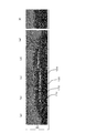
- the area of one conductive layer 126 is, for example, 100 nm 2 or more and 50 ⁇ m 2 or less.
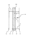
- the width of the auxiliary electrode 124 is, for example, 25 ⁇ m to 100 ⁇ m, preferably 40 ⁇ m to 60 ⁇ m, and the length of the auxiliary electrode 124 is, for example, 10 mm to 200 mm, preferably 50 mm to 100 mm.
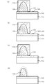
- the auxiliary electrode 124 is formed on the first electrode 120, the second layer 154 is formed on the first layer 152, and the second layer 164 is further formed on the first layer 162.
- the auxiliary electrode 124 and the second layers 154 and 164 are formed using a coating method such as an inkjet method (second step). In this step, the coating material for forming the auxiliary electrode 124 is scattered, and the conductive layer 126 is formed on the first electrode 120.
- the end portion of the insulating layer 170 is gradually thinned.
- the thickness of the portion of the insulating layer 170 that overlaps the auxiliary electrode 124 is substantially constant. For this reason, the auxiliary electrode 124 is sufficiently covered with the insulating layer 170.
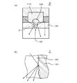
- the position of the conductive layer 126 not covered with the insulating layer 170 is specified (steps S10 and S20 in FIG. 9). Specifically, a voltage in the direction opposite to that during light emission is applied between the first electrode 120 and the second electrode 140 (step S10). The absolute value of the voltage applied at this time is smaller than the absolute value (for example, 12V to 15V) of the voltage for causing the light emitting device 100 to emit light, and is, for example, 1.5V to 3V. Next, the emission point is observed using, for example, an emission microscope, and the coordinates of the emission point on the substrate 110 are recognized (step S20). This light emitting point is caused by a short circuit between the first electrode 120 and the second electrode 140 due to the conductive layer 126.
- the auxiliary wirings 155 and 165 are formed by a coating method, the side surfaces of the auxiliary wirings 155 and 165 are formed when the auxiliary wirings 155 and 165 are formed by using a vapor phase film forming method such as a vapor deposition method and an etching method. In comparison, the auxiliary wirings 155 and 165 are inclined in the direction in which the width increases toward the bottom. Therefore, a gap is hardly generated between the side surfaces of the auxiliary wirings 155 and 165 and the transparent electrode layers 153 and 163.
- auxiliary wirings 155 and 165 are formed using a coating material, even when irregularities occur on the surfaces of the transparent electrode layers 153 and 163 due to the auxiliary wirings 155 and 165, The unevenness becomes smooth. For this reason, the space between the substrate 110 and the sealing member 180 is more easily filled with the adhesive layer 184, and as a result, the sealing ability of the sealing member 180 is further increased. Further, since the auxiliary wiring 155 is provided in the first connection wiring 156 and the auxiliary wiring 165 is further provided in the second connection wiring 166, the resistance of the first connection wiring 156 and the second connection wiring 166 becomes low.
- the space between the substrate 110 and the sealing member 180 is easily filled with the adhesive layer 184, as in the second embodiment. Therefore, the sealing ability by the sealing member 180 is increased.
Landscapes
- Physics & Mathematics (AREA)
- Optics & Photonics (AREA)
- Engineering & Computer Science (AREA)
- Manufacturing & Machinery (AREA)
- Electroluminescent Light Sources (AREA)
Abstract
Description
前記基板上に形成され、透明導電材料からなる第1電極と、
前記第1電極上に形成された補助電極と、
前記第1電極上に形成され、前記補助電極と同じ材料によって形成された島状の導電部と、
前記補助電極及び前記島状の導電部を覆い、かつ前記補助電極と前記島状電極の間を埋めている絶縁層と、
前記絶縁層及び前記第1電極上に形成された有機層と、
前記有機層の上に形成された第2電極と、
を備える発光装置である。
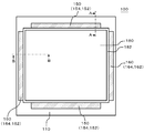
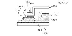
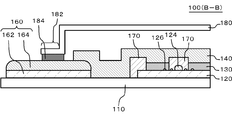
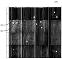
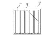
図1、図2、図3、及び図4は、発光装置100の平面図である。図3は、図4から封止部材180を取り除いた図であり、図2は、図3から第2電極140を取り除いた図であり、図1は、図2から有機層130及び絶縁層170を取り除いた図である。本図に示す発光装置100は、照明装置として使用される。
本変形例に係る発光装置100の製造方法は、補助電極124を形成したのちに基板110をエッチングする工程の代わりに、図9に示すリペア工程を有している点を除いて、第1の実施形態に係る発光装置100の製造方法と同様である。図9に示す工程は、第2電極140が形成されたのち、封止部材180が基板110に固定される前に行ってもよいし、封止部材180が固定された後にリペア工程を行ってもよい。
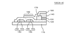
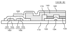
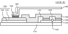
図11は、第2の実施形態に係る発光装置100の構成を示す平面図であり、第1の実施形態における図1に対応している。図12は図11のA-A断面図であり、図13は図11のB-B断面図である。図12及び図13では、説明のため、封止部材180及び接着層184を示している。本実施形態に係る発光装置100は、以下の点を除いて、第1の実施形態に係る発光装置100と同様の構成を有している。
図14、15は、変形例1に係る発光装置100の断面図であり、それぞれ第2の実施形態の図12,13に対応している。本変形例に係る発光装置100は、封止部材180の構成を除いて、第2の実施形態に係る発光装置100と同様の構成である。
図16、17は、変形例2に係る発光装置100の断面図であり、それぞれ第2の実施形態の図12,13に対応している。本変形例に係る発光装置100は、封止部材180が膜である点を除いて、第2の実施形態に係る発光装置100と同様の構成である。
図18は、第3の実施形態に係る発光装置100の構成を示す断面図であり、第1の実施形態における図6に対応している。本実施形態に係る発光装置100は、以下の点を除いて、第1の実施形態に係る発光装置100と同様の構成である。
図20は、第3の実施形態の変形例に係る発光装置100の断面図であり、第3の実施形態の図18に対応している。本変形例に係る発光装置100は、溝122が第1電極120を貫いていない点を除いて、第3の実施形態に係る発光装置100と同様の構成である。本変形例において、溝122は、例えば、透明電極材料をエッチングして第1電極120を形成する工程とは別の工程で形成される。ただし、溝122の幅によっては、第1電極120と同一工程で形成できる場合もある。
Claims (7)
- 基板と、
前記基板上に形成され、透明導電材料からなる第1電極と、
前記第1電極上に形成された補助電極と、
前記第1電極上に形成され、前記補助電極と同じ材料によって形成された島状の導電部と、
前記補助電極及び前記島状の導電部を覆い、かつ前記補助電極と前記島状電極の間を埋めている絶縁層と、
前記絶縁層及び前記第1電極上に形成された有機層と、
前記有機層の上に形成された第2電極と、
を備える発光装置。 - 請求項1に記載の発光装置において、
前記補助電極は、金属粒子を含む塗布材料によって形成されている発光装置。 - 請求項2に記載の発光装置において、
前記島状の導電部の面積は、50μm2以下である発光装置。 - 請求項3に記載の発光装置において、
複数の前記島状の導電部を備え、
一部の前記島状の導電部は、前記絶縁層によって覆われておらず、
前記絶縁層の外に位置する前記島状の導電部の少なくとも表層は、絶縁化または高抵抗化されている発光装置。 - 請求項4に記載の発光装置において、
複数の前記補助電極が互いに平行に延在しており、
前記複数の補助電極の中間地点における前記島状の導電部の密度は、前記補助電極に隣接する領域における前記島状の導電部の密度よりも低い発光装置。 - 請求項5に記載の発光装置において、
前記金属粒子は銀粒子である発光装置。 - 請求項1~6のいずれか一項に記載の発光装置において、
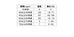
前記補助電極の幅方向において、前記補助電極の中心から前記絶縁層の縁までの距離は、40μm以上60μm以下である発光装置。
Priority Applications (4)
| Application Number | Priority Date | Filing Date | Title |
|---|---|---|---|
| JP2016519151A JP6495253B2 (ja) | 2014-05-16 | 2015-03-31 | 発光装置 |
| KR1020167034494A KR101935122B1 (ko) | 2014-05-16 | 2015-03-31 | 발광 장치 |
| US15/311,814 US10374188B2 (en) | 2014-05-16 | 2015-03-31 | Light-emitting device with auxiliary electrode and adjacent insular conductive portions |
| US16/439,480 US11502269B2 (en) | 2014-05-16 | 2019-06-12 | Light-emitting device with auxiliary electrode and adjacent insular conductive portions |
Applications Claiming Priority (2)
| Application Number | Priority Date | Filing Date | Title |
|---|---|---|---|
| JPPCT/JP2014/063123 | 2014-05-16 | ||
| PCT/JP2014/063123 WO2015173965A1 (ja) | 2014-05-16 | 2014-05-16 | 発光装置 |
Related Child Applications (2)
| Application Number | Title | Priority Date | Filing Date |
|---|---|---|---|
| US15/311,814 A-371-Of-International US10374188B2 (en) | 2014-05-16 | 2015-03-31 | Light-emitting device with auxiliary electrode and adjacent insular conductive portions |
| US16/439,480 Continuation US11502269B2 (en) | 2014-05-16 | 2019-06-12 | Light-emitting device with auxiliary electrode and adjacent insular conductive portions |
Publications (1)
| Publication Number | Publication Date |
|---|---|
| WO2015174154A1 true WO2015174154A1 (ja) | 2015-11-19 |
Family
ID=54479531
Family Applications (2)
| Application Number | Title | Priority Date | Filing Date |
|---|---|---|---|
| PCT/JP2014/063123 Ceased WO2015173965A1 (ja) | 2014-05-16 | 2014-05-16 | 発光装置 |
| PCT/JP2015/060162 Ceased WO2015174154A1 (ja) | 2014-05-16 | 2015-03-31 | 発光装置 |
Family Applications Before (1)
| Application Number | Title | Priority Date | Filing Date |
|---|---|---|---|
| PCT/JP2014/063123 Ceased WO2015173965A1 (ja) | 2014-05-16 | 2014-05-16 | 発光装置 |
Country Status (4)
| Country | Link |
|---|---|
| US (2) | US10374188B2 (ja) |
| JP (5) | JP6495253B2 (ja) |
| KR (1) | KR101935122B1 (ja) |
| WO (2) | WO2015173965A1 (ja) |
Cited By (4)
| Publication number | Priority date | Publication date | Assignee | Title |
|---|---|---|---|---|
| KR20180062109A (ko) * | 2016-11-30 | 2018-06-08 | 엘지디스플레이 주식회사 | 유기발광소자를 이용한 조명장치 및 그 제조방법 |
| EP3333894A1 (en) * | 2016-12-07 | 2018-06-13 | LG Display Co., Ltd. | Light apparatus using organic light-emitting diode and method of fabricating the same |
| KR20180071789A (ko) * | 2016-12-20 | 2018-06-28 | 엘지디스플레이 주식회사 | 유기발광소자를 이용한 조명장치 및 그 제조방법 |
| EP3333925B1 (en) * | 2016-12-07 | 2024-08-21 | LG Display Co., Ltd. | Lighting apparatus using organic light emitting diode |
Families Citing this family (12)
| Publication number | Priority date | Publication date | Assignee | Title |
|---|---|---|---|---|
| KR102712048B1 (ko) * | 2016-11-30 | 2024-09-27 | 엘지디스플레이 주식회사 | 유기발광소자를 이용한 조명장치 및 그 제조방법 |
| KR102321663B1 (ko) * | 2017-07-11 | 2021-11-03 | 엘지디스플레이 주식회사 | 유기발광소자를 이용한 조명장치 및 그 제조방법 |
| KR102315040B1 (ko) * | 2017-07-11 | 2021-10-19 | 엘지디스플레이 주식회사 | 유기발광소자를 이용한 조명장치 및 그 제조방법 |
| KR102387125B1 (ko) * | 2017-07-11 | 2022-04-14 | 엘지디스플레이 주식회사 | 유기발광소자를 이용한 조명장치 |
| KR102321724B1 (ko) * | 2017-07-11 | 2021-11-03 | 엘지디스플레이 주식회사 | 유기발광소자를 이용한 조명장치 및 그 제조방법 |
| KR102340944B1 (ko) * | 2017-07-11 | 2021-12-20 | 엘지디스플레이 주식회사 | 유기발광소자를 이용한 조명장치 및 그 제조방법 |
| KR102441681B1 (ko) * | 2017-12-05 | 2022-09-07 | 엘지디스플레이 주식회사 | 조명 장치용 oled 패널 및 그 제조 방법 |
| TWI677123B (zh) * | 2018-11-29 | 2019-11-11 | 機光科技股份有限公司 | 去定位器及使用該去定位器的發光裝置 |
| CN111244299A (zh) * | 2018-11-29 | 2020-06-05 | 机光科技股份有限公司 | 去定位器及使用该去定位器的发光装置 |
| KR102544067B1 (ko) * | 2018-12-31 | 2023-06-16 | 엘지디스플레이 주식회사 | 유기 조명 장치 |
| KR102581861B1 (ko) * | 2018-12-31 | 2023-09-21 | 엘지디스플레이 주식회사 | 유기 조명 장치 |
| KR102601826B1 (ko) * | 2018-12-31 | 2023-11-13 | 엘지디스플레이 주식회사 | 유기 조명 장치 |
Citations (6)
| Publication number | Priority date | Publication date | Assignee | Title |
|---|---|---|---|---|
| JPH11339970A (ja) * | 1998-05-26 | 1999-12-10 | Tdk Corp | 有機el表示装置 |
| WO2005041217A1 (ja) * | 2003-10-28 | 2005-05-06 | Sumitomo Metal Mining Co., Ltd. | 透明導電積層体とその製造方法及び透明導電積層体を用いたデバイス |
| WO2007029756A1 (ja) * | 2005-09-07 | 2007-03-15 | Asahi Glass Company, Limited | 補助配線付き基体およびその製造方法 |
| JP2010198935A (ja) * | 2009-02-26 | 2010-09-09 | Dowa Electronics Materials Co Ltd | 有機エレクトロルミネッセンス電極の形成方法及び該形成方法を用いて得られた有機エレクトロルミネッセンス構造体 |
| JP2012094348A (ja) * | 2010-10-26 | 2012-05-17 | Idemitsu Kosan Co Ltd | 光電変換装置、及び光電変換装置の製造方法 |
| JP2013541804A (ja) * | 2010-08-23 | 2013-11-14 | コーニンクレッカ フィリップス エヌ ヴェ | 不透明導電性領域の自己整合被覆 |
Family Cites Families (16)
| Publication number | Priority date | Publication date | Assignee | Title |
|---|---|---|---|---|
| JP2002343562A (ja) * | 2001-05-11 | 2002-11-29 | Pioneer Electronic Corp | 発光ディスプレイ装置及びその製造方法 |
| JP2007073305A (ja) * | 2005-09-06 | 2007-03-22 | Harison Toshiba Lighting Corp | 有機el発光装置およびその製造方法 |
| JP2008130449A (ja) | 2006-11-22 | 2008-06-05 | Alps Electric Co Ltd | 発光装置およびその製造方法 |
| JP2008288102A (ja) | 2007-05-18 | 2008-11-27 | Fujifilm Corp | 透明導電性フイルム、透明導電性フイルムの製造方法、透明電極フイルム、色素増感太陽電池、エレクトロルミネッセンス素子及び電子ペーパー |
| RU2507638C2 (ru) * | 2008-10-02 | 2014-02-20 | Конинклейке Филипс Электроникс Н.В. | Устройство oled с покрытой шунтирующей линией |
| CN102172101B (zh) * | 2008-10-06 | 2015-07-08 | 旭硝子株式会社 | 电子器件用基板及其制造方法、使用该基板的电子器件及其制造方法以及有机led元件用基板 |
| KR20120012641A (ko) | 2010-08-02 | 2012-02-10 | 주성엔지니어링(주) | 전기광학장치의 제작 방법 |
| KR20120119091A (ko) * | 2011-04-20 | 2012-10-30 | 삼성디스플레이 주식회사 | 유기 발광 표시 장치와, 이의 제조 방법 |
| US9124461B2 (en) * | 2011-07-18 | 2015-09-01 | Marvell Israel (M.I.S.L) Ltd. | Method and apparatus for reducing jitter |
| JP5915056B2 (ja) | 2011-09-28 | 2016-05-11 | コニカミノルタ株式会社 | 透明電極の製造方法および有機電子デバイスの製造方法 |
| JP5898933B2 (ja) * | 2011-11-29 | 2016-04-06 | 富士フイルム株式会社 | 積層体、及び有機電界発光装置 |
| JP6560494B2 (ja) * | 2012-08-21 | 2019-08-14 | 株式会社ホタルクス | 有機el照明パネル用基板、有機el照明パネル用基板の製造方法、有機el照明パネルおよび有機el照明装置 |
| WO2014041764A1 (ja) * | 2012-09-13 | 2014-03-20 | パナソニック株式会社 | 有機エレクトロルミネッセンス素子 |
| JP6024351B2 (ja) * | 2012-09-28 | 2016-11-16 | コニカミノルタ株式会社 | 導電膜及び有機エレクトロルミネッセンス素子並びに導電膜の製造方法 |
| JP5933495B2 (ja) * | 2012-09-28 | 2016-06-08 | 富士フイルム株式会社 | 有機電界発光素子及び有機電界発光素子の製造方法 |
| JP6295958B2 (ja) | 2012-10-23 | 2018-03-20 | コニカミノルタ株式会社 | 透明電極、電子デバイス及び有機エレクトロルミネッセンス素子 |
-
2014
- 2014-05-16 WO PCT/JP2014/063123 patent/WO2015173965A1/ja not_active Ceased
-
2015
- 2015-03-31 KR KR1020167034494A patent/KR101935122B1/ko not_active Expired - Fee Related
- 2015-03-31 US US15/311,814 patent/US10374188B2/en active Active
- 2015-03-31 WO PCT/JP2015/060162 patent/WO2015174154A1/ja not_active Ceased
- 2015-03-31 JP JP2016519151A patent/JP6495253B2/ja not_active Expired - Fee Related
-
2019
- 2019-03-06 JP JP2019040291A patent/JP2019083214A/ja active Pending
- 2019-06-12 US US16/439,480 patent/US11502269B2/en active Active
-
2021
- 2021-01-13 JP JP2021003281A patent/JP2021061258A/ja active Pending
-
2022
- 2022-08-29 JP JP2022135605A patent/JP2022162150A/ja active Pending
-
2024
- 2024-02-22 JP JP2024025143A patent/JP2024051011A/ja not_active Withdrawn
Patent Citations (6)
| Publication number | Priority date | Publication date | Assignee | Title |
|---|---|---|---|---|
| JPH11339970A (ja) * | 1998-05-26 | 1999-12-10 | Tdk Corp | 有機el表示装置 |
| WO2005041217A1 (ja) * | 2003-10-28 | 2005-05-06 | Sumitomo Metal Mining Co., Ltd. | 透明導電積層体とその製造方法及び透明導電積層体を用いたデバイス |
| WO2007029756A1 (ja) * | 2005-09-07 | 2007-03-15 | Asahi Glass Company, Limited | 補助配線付き基体およびその製造方法 |
| JP2010198935A (ja) * | 2009-02-26 | 2010-09-09 | Dowa Electronics Materials Co Ltd | 有機エレクトロルミネッセンス電極の形成方法及び該形成方法を用いて得られた有機エレクトロルミネッセンス構造体 |
| JP2013541804A (ja) * | 2010-08-23 | 2013-11-14 | コーニンクレッカ フィリップス エヌ ヴェ | 不透明導電性領域の自己整合被覆 |
| JP2012094348A (ja) * | 2010-10-26 | 2012-05-17 | Idemitsu Kosan Co Ltd | 光電変換装置、及び光電変換装置の製造方法 |
Cited By (12)
| Publication number | Priority date | Publication date | Assignee | Title |
|---|---|---|---|---|
| KR20180062109A (ko) * | 2016-11-30 | 2018-06-08 | 엘지디스플레이 주식회사 | 유기발광소자를 이용한 조명장치 및 그 제조방법 |
| EP3346499A1 (en) * | 2016-11-30 | 2018-07-11 | LG Display Co., Ltd. | Lighting apparatus using organic light emitting diode and method of fabricating the same |
| US10290687B2 (en) | 2016-11-30 | 2019-05-14 | Lg Display Co., Ltd. | Lighting apparatus using organic light emitting diode and method of fabricating the same |
| KR102618599B1 (ko) * | 2016-11-30 | 2023-12-27 | 엘지디스플레이 주식회사 | 유기발광소자를 이용한 조명장치 및 그 제조방법 |
| EP3333894A1 (en) * | 2016-12-07 | 2018-06-13 | LG Display Co., Ltd. | Light apparatus using organic light-emitting diode and method of fabricating the same |
| CN108174490A (zh) * | 2016-12-07 | 2018-06-15 | 乐金显示有限公司 | 使用有机发光二极管的照明设备及其制造方法 |
| US10079361B2 (en) | 2016-12-07 | 2018-09-18 | Lg Display Co., Ltd. | Lighting apparatus using organic light-emitting diode and method of fabricating the same |
| CN108174490B (zh) * | 2016-12-07 | 2019-10-25 | 乐金显示有限公司 | 使用有机发光二极管的照明设备及其制造方法 |
| US10529949B2 (en) | 2016-12-07 | 2020-01-07 | Lg Display Co., Ltd. | Lighting apparatus using organic light-emitting diode and method of fabricating the same |
| EP3333925B1 (en) * | 2016-12-07 | 2024-08-21 | LG Display Co., Ltd. | Lighting apparatus using organic light emitting diode |
| KR20180071789A (ko) * | 2016-12-20 | 2018-06-28 | 엘지디스플레이 주식회사 | 유기발광소자를 이용한 조명장치 및 그 제조방법 |
| KR102661550B1 (ko) | 2016-12-20 | 2024-04-26 | 엘지디스플레이 주식회사 | 유기발광소자를 이용한 조명장치 및 그 제조방법 |
Also Published As
| Publication number | Publication date |
|---|---|
| US10374188B2 (en) | 2019-08-06 |
| US11502269B2 (en) | 2022-11-15 |
| US20200006696A1 (en) | 2020-01-02 |
| JPWO2015174154A1 (ja) | 2017-04-20 |
| JP2021061258A (ja) | 2021-04-15 |
| JP6495253B2 (ja) | 2019-04-03 |
| JP2022162150A (ja) | 2022-10-21 |
| JP2024051011A (ja) | 2024-04-10 |
| JP2019083214A (ja) | 2019-05-30 |
| KR101935122B1 (ko) | 2019-01-03 |
| WO2015173965A1 (ja) | 2015-11-19 |
| US20170092891A1 (en) | 2017-03-30 |
| KR20170007699A (ko) | 2017-01-19 |
Similar Documents
| Publication | Publication Date | Title |
|---|---|---|
| JP6495253B2 (ja) | 発光装置 | |
| KR102453921B1 (ko) | 유기 발광 표시 장치 및 그 제조 방법 | |
| CN109841749B (zh) | 有机发光装置 | |
| CN100442569C (zh) | 采用多层型像素电极的有机电致发光器件及其制造方法 | |
| JPWO2014162395A1 (ja) | 発光装置 | |
| JP6463354B2 (ja) | 発光装置 | |
| TWI489625B (zh) | 有機發光顯示面板及其製作方法 | |
| JP2015220089A (ja) | 発光装置の製造方法 | |
| JP2015220091A (ja) | 発光装置 | |
| JP2016192342A (ja) | 発光装置 | |
| JP2020035755A (ja) | 発光装置 | |
| JP2015220090A (ja) | 発光装置 | |
| JP2018077499A (ja) | 光学装置 | |
| CN103190201A (zh) | 有机el面板及其制造方法 | |
| JP2015220088A (ja) | 発光装置の製造方法 | |
| JP2015162444A (ja) | 発光装置 | |
| JP6294071B2 (ja) | 発光装置 | |
| JP2016046141A (ja) | 発光装置 | |
| JP2023108047A (ja) | 発光装置 | |
| JP2015225694A (ja) | 発光装置 | |
| WO2014141463A1 (ja) | 発光装置及び発光装置の検査方法 | |
| JP2018156722A (ja) | 有機elパネル | |
| WO2015125309A1 (ja) | 発光装置 | |
| JP2008117585A (ja) | 有機エレクトロルミネッセンス素子 | |
| WO2014162387A1 (ja) | ワイヤの接続構造及び電気機器 |
Legal Events
| Date | Code | Title | Description |
|---|---|---|---|
| 121 | Ep: the epo has been informed by wipo that ep was designated in this application |
Ref document number: 15792226 Country of ref document: EP Kind code of ref document: A1 |
|
| ENP | Entry into the national phase |
Ref document number: 2016519151 Country of ref document: JP Kind code of ref document: A |
|
| NENP | Non-entry into the national phase |
Ref country code: DE |
|
| WWE | Wipo information: entry into national phase |
Ref document number: 15311814 Country of ref document: US |
|
| ENP | Entry into the national phase |
Ref document number: 20167034494 Country of ref document: KR Kind code of ref document: A |
|
| 122 | Ep: pct application non-entry in european phase |
Ref document number: 15792226 Country of ref document: EP Kind code of ref document: A1 |