WO2015170491A1 - 信号処理装置及び通信装置 - Google Patents
信号処理装置及び通信装置 Download PDFInfo
- Publication number
- WO2015170491A1 WO2015170491A1 PCT/JP2015/053754 JP2015053754W WO2015170491A1 WO 2015170491 A1 WO2015170491 A1 WO 2015170491A1 JP 2015053754 W JP2015053754 W JP 2015053754W WO 2015170491 A1 WO2015170491 A1 WO 2015170491A1
- Authority
- WO
- WIPO (PCT)
- Prior art keywords
- signal
- input
- analog
- output
- digital
- Prior art date
- Legal status (The legal status is an assumption and is not a legal conclusion. Google has not performed a legal analysis and makes no representation as to the accuracy of the status listed.)
- Ceased
Links
Images
Classifications
-
- H—ELECTRICITY
- H03—ELECTRONIC CIRCUITRY
- H03M—CODING; DECODING; CODE CONVERSION IN GENERAL
- H03M1/00—Analogue/digital conversion; Digital/analogue conversion
- H03M1/12—Analogue/digital converters
- H03M1/50—Analogue/digital converters with intermediate conversion to time interval
- H03M1/56—Input signal compared with linear ramp
Definitions
- the present invention relates to a signal processing apparatus and a communication apparatus having a ⁇ modulator.
- Non-Patent Document 1 describes a direct RF undersampling reception method.
- FIG. 6 shows a receiver described in Non-Patent Document 1.
- the receiver 100 includes a low noise amplifier 101, a band pass filter (anti-aliasing filter) 102, a sample and hold circuit 103, and an AD converter 104. 5 down-converts the received RF signal into an intermediate frequency (IF) signal by undersampling.
- the sample and hold circuit 103 of the receiver 100 samples the output signal from the bandpass filter at the sampling frequency fs, and maintains the signal value at the time of sampling.
- the AD converter 104 to which the output signal from the sample and hold circuit 103 is input outputs a digital IF signal.
- the sampling frequency fs of the sample and hold circuit may be smaller than the carrier frequency fc of the RF signal. Therefore, the processing speed of the AD converter 104 and the like can be suppressed to save power.
- the AD converter 104 is necessary next to the sample and hold circuit 103.
- a circuit including an analog element called the AD converter 104 is required. Since a general AD converter includes analog elements, if the AD converter 104 is necessary, digitization of the circuit is hindered.
- an object of the present invention is to reduce analog elements when AD conversion is performed.
- a comparator that compares an analog input signal and an analog reference signal, a digital reference signal corresponding to the analog reference signal, and the analog input signal and the analog reference signal are generated by the comparator.
- a generator that outputs the value of the digital reference signal when a match with the analog reference signal is detected as a digital value of the analog input signal, and ⁇ modulation that ⁇ modulates the digital reference signal generated by the generator And a component of the analog reference signal included in the output signal among the output signals of the ⁇ modulator, and a pass signal provided to the comparator as the analog reference signal.
- analog elements can be reduced.
- a signal processing device generates a digital reference signal corresponding to a comparator that compares an analog input signal and an analog reference signal, and the analog input by the comparator.
- a generator for outputting a value of the digital reference signal when a match between the signal and the analog reference signal is detected as a digital value of the analog input signal; and ⁇ modulation of the digital reference signal generated by the generator And a component of the analog reference signal included in the output signal among the output signals of the ⁇ modulator, and a passing signal provided to the comparator as the analog reference signal A first filter.
- the ⁇ modulator and the first filter can perform the same operation as that of the DA converter, and thus can perform the same operation as that of the AD converter using the DA converter.
- a delta-sigma modulator can be comprised with a digital circuit, an analog element can be decreased compared with the case where a DA converter is used.
- a communication device includes a sample and hold circuit to which a reception signal is input and the signal processing device of (1), and an output signal of the sample and hall circuit is the analog input signal. As given to the comparator. According to the above configuration, it is possible to obtain a communication device with fewer analog elements than a conventional receiver.
- the ⁇ modulator includes a first input port to which the digital reference signal is input, a second input port to which a sampling clock is input, a first loop filter, a second loop filter, and the first An adder for adding the outputs of the loop filter and the second loop filter; and a quantizer for quantizing the output of the adder, wherein the first loop filter is input to the first input port.
- the digital reference signal and a feedback signal output from the quantizer are input, and the second loop filter includes the sampling clock input to the second input port, and the quantization And the first loop filter blocks noise near the frequency of the digital reference signal.
- the second loop filter has a characteristic of blocking noise near the frequency of the sampling clock, and the sampling clock component included in the output signal among the output signals of the ⁇ modulator.
- a second filter provided to pass the passing signal as a sampling clock to the sample and hold circuit. According to the above configuration, not only the reference signal but also the sampling clock of the sample and hold circuit can be output from the ⁇ modulator.
- the ⁇ modulator includes a first input port to which the digital reference signal is input, a third port to which a digital transmission signal corresponding to an analog transmission signal transmitted from the communication device is input, and a first port A loop filter; a third loop filter; an adder that adds outputs of the first loop filter and the third loop filter; and a quantizer that quantizes an output of the adder.
- a loop filter is provided to receive the digital reference signal input to the first input port and a feedback signal output from the quantizer, and the third loop filter is input to the third port.
- the input digital transmission signal and a feedback signal of the output of the quantizer are provided to be input, and the first loop filter is the digital reference
- the third loop filter has a characteristic of blocking noise near the frequency of the digital transmission signal, and the output of the ⁇ modulator is the output signal.
- the apparatus further includes a third filter configured to pass the component of the analog transmission signal included in the signal so that the passing signal becomes the analog transmission signal transmitted from the communication device. . According to the above configuration, not only the reference signal but also the transmission signal can be output from the ⁇ modulator.
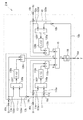
- FIG. 1 shows a communication device (receiver) 1 according to the first embodiment.
- the communication device 1 transmits and receives a radio signal (RF signal).
- RF signal a radio signal
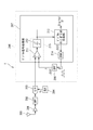
- 1 includes an antenna 200, a low noise amplifier (LNA) 201, a band pass filter (anti-aliasing filter) 202, a sample and hold circuit (S / H) 203, a clock generator 204, and a signal processing device 206. It has.
- a sampling clock (frequency fs) of the sample and hold circuit 203 is generated by the clock generator 204.
- the communication device 1 shown in FIG. 1 is obtained by replacing the AD converter 104 of the receiver 100 shown in FIG. 6 with a signal processing device 206. Like the receiver 100 shown in FIG. Downconverted to IF signal by undersampling.
- the sample and hold circuit 203 performs processing to sample and hold the output signal (RF signal (received signal)) from the bandpass filter 202 at the sampling frequency fs.
- the signal processing device 206 to which the output signal from the sample and hold circuit 203 is input generates a digital IF signal from the output signal of the sample and hold circuit 203 and performs digital signal processing on the digital IF signal. Since the communication apparatus 1 also performs undersampling, the sampling frequency fs of the sample and hold circuit 203 may be smaller than the carrier frequency fc of the RF signal.
- the signal processing device 206 includes a digital signal processing unit 207 and a first band pass filter (analog BPF) 208.
- the digital signal processing unit 207 generates a digital IF signal by using a subtractor 211, a quantizer 212, a digital sawtooth (digital reference signal) generation unit 213, a bandpass ⁇ modulator (DSM) 214, It is equipped with.
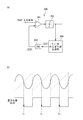
- the signal processing device 206 (the first bandpass filter 208, the difference unit 211, the quantizer 212, the digital sawtooth wave generation unit 213, and the ⁇ modulator 214) shown in FIG. 1 has an AD as shown in FIG. It can be understood that the DA converter 304 in the converter 300 is replaced with the ⁇ modulator 214 and the first band pass filter 208.
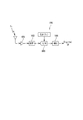
- the AD converter 300 illustrated in FIG. 2A includes a differencer 301, a quantizer 302, a digital sawtooth wave generation unit 303, and a DA converter 304.
- the differencer 301 receives an analog input signal and an analog sawtooth wave (analog reference signal), and outputs a difference between the analog input signal and the analog reference signal.
- the quantizer 302 quantizes the output of the subtractor 301 to two levels, Low or High.
- the digital sawtooth wave generated by the digital sawtooth wave generation unit 303 is converted into an analog sawtooth wave by the DA converter 204 and given to one input of the differencer 301.
- the quantizer 302 outputs a high level if the output of the differentiator 301 is greater than zero, and outputs a low level if the output of the differentiator 301 is smaller than zero. Therefore, when the magnitude of the analog input signal and the magnitude of the analog sawtooth wave coincide with each other, the output of the quantizer 302 is switched between the High and Low levels (see FIG. 2B).
- the timing at which the magnitude of the analog input signal and the magnitude of the analog sawtooth wave coincide with each other is the falling timings t 1 , t 2 , and t 3 of the output signal of the quantizer 302.
- the output signal of the quantizer 302 is supplied to the digital sawtooth wave generation unit 204.
- the generation unit 303 outputs the magnitude (digital value) of the digital sawtooth wave at these timings t 1 , t 2 , and t 3 as a digital value of the analog input signal.
- the 2A uses a DA converter 304, and the DA converter 304 includes a relatively large number of analog elements.
- the DA converter 304 instead of the DA converter 304, a ⁇ modulator 214 and a first band pass filter 208 are employed.
- the ⁇ modulator 214 performs digital processing and can be provided in the digital signal processing unit 207. Therefore, when the ⁇ modulator 214 and the first band pass filter 208 are employed instead of the DA converter 304, the analog elements only need to be the first band pass filter 208, and the analog elements can be reduced.
- the difference unit 211 outputs the difference between the two input signals.
- the quantizer 212 quantizes the output of the subtractor 211 to two levels of Low or High.
- the quantizer 212 outputs a high level if the output of the differentiator 211 is greater than zero, and outputs a low level if the output of the differentiator 211 is smaller than zero.
- the subtractor 211 and the quantizer 212 compare the S / H signal with the passing signal (analog sawtooth wave; analog reference signal) of the bandpass filter 21 and detect the coincidence of both signals. It is a container 215.
- the output signal of the quantizer 212 is supplied to the digital sawtooth wave generation unit 213.
- the generation unit 213 outputs the magnitude (digital value) of the digital sawtooth wave at these timings t 1 , t 2 , and t 3 as a digital value of the analog input signal.
- This digital value is a digital IF signal obtained by down-converting the RF signal (received signal) received by the communication device 1.
- the signal output from the digital sawtooth wave generation unit 213 does not need to be an IF signal, and may be a baseband signal.
- the bandpass ⁇ modulator 214 receives a digital sawtooth wave (digital reference signal) as an input, and outputs a pulse signal having an analog sawtooth wave (analog reference signal) as a signal component.
- the first band pass filter 208 is configured to block the passage of the quantization noise component included in the pulse signal output from the ⁇ modulator 214 and pass the signal component of the analog sawtooth wave.
- the first band pass filter 208 is connected to one input of the subtractor 211, and can pass the pass signal (analog sawtooth wave) of the first band pass filter 208 to the subtractor 211.
- FIG. 4 shows a communication device 1 according to the second embodiment.
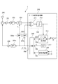
- the communication device 1 shown in FIG. 1 mainly shows only the function of the communication device 1 as a receiver, but FIG. 4 shows the functions of the communication device 1 as a receiver and a transmitter. Note that points not particularly described in the second embodiment are the same as those in the first embodiment.
- the delta-sigma modulator 214 of 2nd Embodiment can output the pulse signal which has all the analog signal components corresponding to each digital signal input from several input port 10a, 10b, 10c from the single output port 10d. it can. Details of the ⁇ modulator 214 will be described later.
- the digital sawtooth wave (first input signal) generated by the digital sawtooth wave generation unit 213 is input to the first input port 10 a of the ⁇ modulator 214.
- the clock (second input signal) having the frequency fs generated by the clock generator 217 is input to the second input port 10b.
- a digital transmission signal (digital modulation signal; digital RF signal) generated by the quadrature modulator 216 is input to the third input port 10c.
- the quadrature modulator 216 performs digital quadrature modulation on the baseband signals I and Q to generate a digital transmission signal (digital modulation signal). Note that the quadrature modulator 216 may be a modulator that performs modulation by another method.
- the pulse signal output from the output port 10d of the ⁇ modulator 214 includes an analog sawtooth wave signal component, a frequency fs clock signal component, and an analog transmission signal (analog modulation signal; analog RF signal) signal. And ingredients.
- the pulse signal output from the ⁇ modulator 214 is transmitted to the second bandpass filter (second filter) 208b and the third bandpass filter (third filter) 208c in addition to the first bandpass filter (first filter) 208a.
- the first band pass filter 208a is connected to one input of the subtractor 211 in the same manner as the first band pass filter 208 of FIG.
- the first band-pass filter 208a is configured to prevent the quantization noise component and other unnecessary signal components included in the pulse signal output from the ⁇ modulator 214 from passing, and pass the signal component of the analog sawtooth wave. Has been.
- the second band pass filter 208b is configured to block the passage of the quantization noise component and other unnecessary signal components included in the pulse signal output from the ⁇ modulator 214 and to pass the clock component of the frequency fs. ing.
- the passing signal (frequency fs clock) of the second band pass filter 208 b is given as a sampling clock of the sample and hold circuit 203.
- the third band pass filter 208c is configured to block the passage of the analog transmission signal component by blocking the passage of the quantization noise component and other unnecessary signal components included in the pulse signal output from the ⁇ modulator 214. Yes.
- a passing signal (analog transmission signal) of the third band pass filter 208c is output from the antenna 200 via the amplifier 209 and the like.
- the path from the antenna 200 to the digital sawtooth wave generation unit 213 has a function as a receiver
- the path from the orthogonal modulation unit 216 to the antenna 200 has a function as a transmitter.
- the sampling clock of the sample and hold circuit 203 can be output from the ⁇ modulator 214, it is not necessary to separately provide the clock generator 204 in FIG. Further, since both the sawtooth wave and the sampling clock are generated by the signal processing unit 206, the sawtooth wave and the sampling clock are compared with the case where the signal processing unit 206 and the clock generator 204 are separated as shown in FIG. Is easy to synchronize.
- FIG. 5 shows a three-input ⁇ modulator 214 used as the ⁇ modulator 214 shown in FIG. ⁇ modulator 214 of FIG. 5, the first input port 10a of the first input signal U 1 is input, a second input port 10b of the second input signal U 2 is input, the third input signal U 3 is input A third input port 10c and a single output port 10d for outputting a pulse signal.
- the ⁇ modulator 214 includes a plurality of loop filters (first loop filter 11, second loop filter 12, third loop filter 13) corresponding to each of the plurality of input ports 10 a, 10 b, 10 c, an adder 15, a quantum Generator 16.
- the plurality of loop filters 11, 12, 13 are quantizers via first input units 11a, 12a, 13a connected to corresponding input ports 10a, 10b, 10c and feedback paths 18a, 18b, 18c, respectively. And 16 second output portions 11b, 12b, 13b connected to the output side.
- Input signals U 1 , U 2 , U 3 input to the corresponding input ports 10a, 10b, 10c are input to the first input units 11a, 12a, 13a.
- the feedback signal V of the output V of the quantizer 16 is input to the second input units 11b, 12b, and 13b.
- the plurality of loop filters 11, 12, and 13 include differentiators 110a, 120a, and 130a, respectively.
- the differentiators 110a, 120a, and 130a include first paths 110d, 120d, and 130d connected to the first input units 11a, 12a, and 13a, and second units connected to the second input units 11b, 12b, and 13b, respectively.
- the paths 110e, 120e, and 130e are connected.
- the differentiators 110a, 120a, and 130a respectively obtain differences U 1 ⁇ V, U 2 ⁇ V, and U 3 ⁇ V between the input signals U 1 , U 2 , and U 3 and the feedback signal V from the quantizer 16.
- Differences U 1 -V, U 2 -V, U 3 -V obtained by the differentiators 110a, 120a, and 130a are input to internal filters 110b, 120b, and 130b provided in the loop filters 11, 12, and 13, respectively.
- the transfer function of the internal filter 110b of the first loop filter 11 is expressed as L 1 (z)
- the transfer function of the internal filter 120b of the second loop filter 12 is expressed as L 2 (z)
- the transfer function of the 13 internal filters 130b is expressed as L 3 (z).
- Outputs L 1 (z) (U 1 (z) ⁇ V (z)), L 2 (z) (U 2 (z) ⁇ V (z)), L 3 (z) of each internal filter 110b, 120b, 130b ) (U 3 (z) ⁇ V (z)) is applied to the adders 110c, 120c, and 130c provided in the loop filters 11, 12, and 13, respectively.
- Each of the adders 110c, 120c, and 130c has a feed-forward path for inputting the input signals U 1 , U 2 , and U 3 input to the first input units 11a, 12a, and 13a to the adders 110c, 120c, and 130c. 110f, 120f, and 130f are connected.
- each adder 110c, 120c, 130c has the input signals U 1 , U 2 , U 3 and the output L 1 (z) (U 1 (z) -V (z)) of the internal filters 110b, 120b, 130b. , L 2 (z) (U 2 (z) ⁇ V (z)) and L 3 (z) (U 3 (z) ⁇ V (z)).
- Outputs of the adders 110c, 120c, and 130c (outputs of the loop filters 11, 12, and 13) Y 1 , Y 2 , and Y 3 are added by the adder 15.
- the output Y of the adder 15 is given to the quantizer 16.
- the quantizer 16 of the present embodiment is a two-level quantizer and outputs a 1-bit pulse train as a quantized signal ( ⁇ modulation signal) V.
- This quantized signal V becomes an output signal of the ⁇ modulator 1.
- the output signal V is given to each loop filter 11, 12, 13 via feedback paths 18a, 18b, 18c.
- Equation (1) STF i (z) is the i-th signal transfer function for the i-th input signal U i (z), and NTF (z) is the noise transfer function for the entire ⁇ modulator 214, E (z) is a noise transfer function.
- the internal filter 110b of the first loop filter 11 has a transfer function L 1 (z) expressed using the first noise transfer function NTF 1 (z).
- the first noise transfer function NTF 1 (z) is a characteristic (band) that suppresses quantization noise in the frequency (band) of the first input signal (digital sawtooth wave) U 1 (z) input to the first loop filter 11. Stop characteristic).
- the internal filter 120b of the second loop filter 12 has a transfer function L 2 (z) indicated by using the second noise transfer function NTF 2 (z).
- the second noise transfer function NTF 2 (z) is a characteristic (band stop characteristic) that suppresses quantization noise in the frequency (band) of the second input signal (clock) U 2 (z) input to the second loop filter 12. ).
- the internal filter 130b of the third loop filter 12 has a transfer function L 3 (z) indicated by using the third noise transfer function NTF 3 (z).
- the third noise transfer function NTF 3 (z) is a characteristic (band) that suppresses quantization noise in the frequency (band) of the third input signal (digital transmission signal) U 3 (z) input to the third loop filter 13. Stop characteristic).
- the ⁇ modulator 214 configured as described above can simultaneously output the signals input to the plurality of input ports 10a, 10b, and 10c in one single output signal V (z).
Landscapes
- Engineering & Computer Science (AREA)
- Theoretical Computer Science (AREA)
- Analogue/Digital Conversion (AREA)
- Compression, Expansion, Code Conversion, And Decoders (AREA)
Abstract
AD変換を行う場合のアナログ要素を低減する。アナログ入力信号とアナログ参照信号との比較を行う比較器215と、アナログ参照信号に対応するデジタル参照信号を生成するとともに、比較器215によりアナログ入力信号とアナログ参照信号との一致が検出されたときのデジタル参照信号の値をアナログ入力信号のデジタル値として出力する生成器213と、生成器213により生成されたデジタル参照信号をΔΣ変調するΔΣ変調器214と、ΔΣ変調器214の出力信号のうち、出力信号に含まれるアナログ参照信号の成分を通過させるよう構成され、通過信号をアナログ参照信号として比較器215に与えるよう設けられた第1フィルタ208と、を備えている信号処理装置。
Description
本発明は、ΔΣ変調器を有する信号処理装置及び通信装置に関するものである。
非特許文献1には、ダイレクトRFアンダーサンプリング受信方法が記載されている。図6は、非特許文献1記載の受信機を示している。この受信機100は、ローノイズアンプ101と、バンドパスフィルタ(アンチエイリアシングフィルタ)102と、サンプルアンドホールド回路103と、ADコンバータ104と、を備えている。図5の受信機100は、受信したRF信号を、アンダーサンプリングによって、中間周波数(Intermediate Frequency;IF)信号へダウンコンバートする。受信機100のサンプルアンドホールド回路103は、バンドパスフィルタからの出力信号をサンプリング周波数fsにてサンプリングし、サンプリング時の信号値を維持する。サンプルアンドホールド回路103からの出力信号が入力されるADコンバータ104は、デジタルIF信号を出力する。
非特許文献1の受信機では、アンダーサンプリングを行うため、サンプルアンドホールド回路のサンプリング周波数fsは、RF信号のキャリア周波数fcよりも小さくても良い。したがって、ADコンバータ104などの処理速度を抑えて、省電力化を図ることができる。
Daliso BANDA et al.,"Direct RF Under Sampling Reception Method with Lower Sampling Frequency",2013 Asia-Pacific Micorwave Conference Proceedings,IEEE, 2013
図6に示す受信機100では、サンプルアンドホールド回路103の次にADコンバータ104が必要である。ADコンバータ104から出力されたデジタルIF信号を処理することになるデジタル信号処理部とは別にADコンバータ104というアナログ要素を含む回路が必要となる。一般的なADコンバータは、アナログ要素を含むため、ADコンバータ104が必要であると、回路のデジタル化が妨げられる。
そこで、本発明は、AD変換を行う場合のアナログ要素を低減することを目的とする。
一の観点からみた本発明は、アナログ入力信号とアナログ参照信号との比較を行う比較器と、前記アナログ参照信号に対応するデジタル参照信号を生成するとともに、前記比較器により前記アナログ入力信号と前記アナログ参照信号との一致が検出されたときの前記デジタル参照信号の値を前記アナログ入力信号のデジタル値として出力する生成器と、前記生成器により生成された前記デジタル参照信号をΔΣ変調するΔΣ変調器と、前記ΔΣ変調器の出力信号のうち、前記出力信号に含まれる前記アナログ参照信号の成分を通過させるよう構成され、通過信号を前記アナログ参照信号として前記比較器に与えるよう設けられた第1フィルタと、を備えている信号処理装置である。
本発明によれば、アナログ要素を低減することができる。
以下、本発明の好ましい実施形態について図面を参照しながら説明する。
[1.実施形態の概要]
(1)実施形態に係る信号処理装置は、アナログ入力信号とアナログ参照信号との比較を行う比較器と、前記アナログ参照信号に対応するデジタル参照信号を生成するとともに、前記比較器により前記アナログ入力信号と前記アナログ参照信号との一致が検出されたときの前記デジタル参照信号の値を前記アナログ入力信号のデジタル値として出力する生成器と、前記生成器により生成された前記デジタル参照信号をΔΣ変調するΔΣ変調器と、前記ΔΣ変調器の出力信号のうち、前記出力信号に含まれる前記アナログ参照信号の成分を通過させるよう構成され、通過信号を前記アナログ参照信号として前記比較器に与えるよう設けられた第1フィルタと、を備えている。上記構成によれば、ΔΣ変調器と第1フィルタとで、DAコンバータと同様の動作を行うことができ、したがって、DAコンバータを利用したADコンバータと同様の動作を行うことができる。そして、ΔΣ変調器はデジタル回路で構成できるため、DAコンバータを用いる場合に比べてアナログ要素を少なくできる。
(1)実施形態に係る信号処理装置は、アナログ入力信号とアナログ参照信号との比較を行う比較器と、前記アナログ参照信号に対応するデジタル参照信号を生成するとともに、前記比較器により前記アナログ入力信号と前記アナログ参照信号との一致が検出されたときの前記デジタル参照信号の値を前記アナログ入力信号のデジタル値として出力する生成器と、前記生成器により生成された前記デジタル参照信号をΔΣ変調するΔΣ変調器と、前記ΔΣ変調器の出力信号のうち、前記出力信号に含まれる前記アナログ参照信号の成分を通過させるよう構成され、通過信号を前記アナログ参照信号として前記比較器に与えるよう設けられた第1フィルタと、を備えている。上記構成によれば、ΔΣ変調器と第1フィルタとで、DAコンバータと同様の動作を行うことができ、したがって、DAコンバータを利用したADコンバータと同様の動作を行うことができる。そして、ΔΣ変調器はデジタル回路で構成できるため、DAコンバータを用いる場合に比べてアナログ要素を少なくできる。
(2)実施形態に係る通信装置は、受信信号が入力されるサンプルアンドホールド回路と、前記(1)の信号処理装置と、を備え、前記サンプルアンドホール回路の出力信号が、前記アナログ入力信号として前記比較器に与えられる。上記構成によれば従来の受信機に比べてアナログ要素の少ない通信装置が得られる。
(3)前記ΔΣ変調器は、前記デジタル参照信号が入力される第1入力ポートと、サンプリングクロックが入力される第2入力ポートと、第1ループフィルタと、第2ループフィルタと、前記第1ループフィルタ及び前記第2ループフィルタの出力を加算する加算器と、前記加算器の出力を量子化する量子化器と、を備え、前記第1ループフィルタは、前記第1入力ポートに入力された前記デジタル参照信号と、前記量子化器の出力のフィードバック信号と、が入力されるように設けられ、前記第2ループフィルタは、前記第2入力ポートに入力された前記サンプリングクロックと、前記量子化器の出力の前記フィードバック信号と、が入力されるように設けられ、前記第1ループフィルタは、前記デジタル参照信号の周波数付近の雑音を阻止する特性を有し、前記第2ループフィルタは、前記サンプリングクロックの周波数付近の雑音を阻止する特性を有し、前記ΔΣ変調器の出力信号のうち、前記出力信号に含まれる前記サンプリングクロックの成分を通過させるよう構成され、通過信号をサンプリングクロックとして前記サンプルアンドホールド回路に与えるよう設けられた第2フィルタを更に備えているのが好ましい。上記構成によれば、ΔΣ変調器から参照信号だけでなくサンプルアンドホールド回路のサンプリングクロックも出力することができる。
(4)前記ΔΣ変調器は、前記デジタル参照信号が入力される第1入力ポートと、前記通信装置から送信されるアナログ送信信号に対応したデジタル送信信号が入力される第3ポートと、第1ループフィルタと、第3ループフィルタと、前記第1ループフィルタ及び前記第3ループフィルタの出力を加算する加算器と、前記加算器の出力を量子化する量子化器と、を備え、前記第1ループフィルタは、前記第1入力ポートに入力された前記デジタル参照信号と、前記量子化器の出力のフィードバック信号と、が入力されるよう設けられ、前記第3ループフィルタは、前記第3ポートに入力された前記デジタル送信信号と、前記量子化器の出力のフィードバック信号と、が入力されるよう設けられ、前記第1ループフィルタは、前記デジタル参照信号の周波数付近の雑音を阻止する特性を有し、前記第3ループフィルタは、前記デジタル送信信号の周波数付近の雑音を阻止する特性を有し、前記ΔΣ変調器の出力信号のうち、前記出力信号に含まれる前記アナログ送信信号の成分を通過させるよう構成された、通過信号が前記通信装置から送信される前記アナログ送信信号となるように設けられた第3フィルタを更に備えているのが好ましい。上記構成によれば、ΔΣ変調器から参照信号だけでなく送信信号も出力することができる。
[2.実施形態の詳細]
[2.1 第1実施形態]
図1は、第1実施形態に係る通信装置(受信機)1を示している。通信装置1は、例えば、無線信号(RF信号)の送受信を行う。図1に示す通信装置1は、アンテナ200、ローノイズアンプ(LNA)201、バンドパスフィルタ(アンチエイリアシングフィルタ)202、サンプルアンドホールド回路(S/H)203、クロック発生器204、及び信号処理装置206を備えている。サンプルアンドホールド回路203のサンプリングクロック(周波数fs)は、クロック発生器204によって生成される。
[2.1 第1実施形態]
図1は、第1実施形態に係る通信装置(受信機)1を示している。通信装置1は、例えば、無線信号(RF信号)の送受信を行う。図1に示す通信装置1は、アンテナ200、ローノイズアンプ(LNA)201、バンドパスフィルタ(アンチエイリアシングフィルタ)202、サンプルアンドホールド回路(S/H)203、クロック発生器204、及び信号処理装置206を備えている。サンプルアンドホールド回路203のサンプリングクロック(周波数fs)は、クロック発生器204によって生成される。
図1に示す通信装置1は、図6に示す受信機100のADコンバータ104を、信号処理装置206に置換したものであり、図6に示す受信機100と同様に、受信したRF信号を、アンダーサンプリングによって、IF信号へダウンコンバートする。
サンプルアンドホールド回路203は、バンドパスフィルタ202からの出力信号(RF信号(受信信号))をサンプリング周波数fsにてサンプルアンドホールドする処理を行う。サンプルアンドホールド回路203からの出力信号が入力される信号処理装置206は、サンプルアンドホールド回路203の出力信号から、デジタルIF信号を生成し、デジタルIF信号に対してデジタル信号処理を行う。この通信装置1も、アンダーサンプリングを行うため、サンプルアンドホールド回路203のサンプリング周波数fsは、RF信号のキャリア周波数fcよりも小さくても良い。
信号処理装置206は、デジタル信号処理部207と、第1バンドパスフィルタ(アナログBPF)208と、を備えている。デジタル信号処理部207は、デジタルIF信号の生成のために、差分器211と、量子化器212と、デジタルのこぎり波(デジタル参照信号)生成部213と、バンドパスΔΣ変調器(DSM)214と、を備えている。図1に示す信号処理装置206(第1バンドパスフィルタ208、差分器211、量子化器212、デジタルのこぎり波生成部213、及びΔΣ変調器214)は、図2(a)に示すようなADコンバータ300におけるDAコンバータ304を、ΔΣ変調器214及び第1バンドパスフィルタ208に置換したものとして理解することができる。
図2(a)に示すADコンバータ300は、差分器301と、量子化器302と、デジタルのこぎり波生成部303と、DAコンバータ304と、を備えている。差分器301は、アナログ入力信号と、アナログのこぎり波(アナログ参照信号)と、が入力され、アナログ入力信号とアナログ参照信号との差分を出力する。量子化器302は、差分器301の出力をLow又はHighの2レベルに量子化する。デジタルのこぎり波生成部303が生成したデジタルのこぎり波は、DAコンバータ204によって、アナログのこぎり波に変換され、差分器301の一方の入力に与えられる。量子化器302は、例えば、差分化器301の出力がゼロよりも大きければHighレベルを出力し、差分化器301の出力がゼロよりも小さければLowレベルを出力する。したがって、アナログ入力信号の大きさとアナログのこぎり波の大きさと、が一致したときに量子化器302の出力は、High-Lowレベル間で切り替わることになる(図2(b)参照)。図2(b)では、アナログ入力信号の大きさとアナログのこぎり波の大きさと、が一致したタイミングは、量子化器302の出力信号の立下りのタイミングt1,t2,t3となる。量子化器302の出力信号は、デジタルのこぎり波生成部204に与えられる。生成部303は、これらのタイミングt1,t2,t3におけるデジタルのこぎり波の大きさ(デジタル値)を、アナログ入力信号のデジタル値として出力する。
図2(a)に示すADコンバータ300は、DAコンバータ304を利用したものであり、DAコンバータ304は比較的多くのアナログ要素を含む。これに対し、図1では、DAコンバータ304に代えて、ΔΣ変調器214及び第1バンドパスフィルタ208が採用されている。ΔΣ変調器214は、デジタル処理を行うものであり、デジタル信号処理部207中に設けることができる。したがって、DAコンバータ304に代えて、ΔΣ変調器214及び第1バンドパスフィルタ208を採用すると、アナログ要素は第1バンドパスフィルタ208があればよく、アナログ要素の削減が可能である。
図1の差分器211には、サンプルアンドホールド回路203の出力信号(S/H信号;アナログ入力信号)と、バンドパスフィルタ208の通過信号(アナログのこぎり波;アナログ参照信号)と、が入力され、差分器211は、両入力信号の差分を出力する。量子化器212は、差分器211の出力をLow又はHighの2レベルに量子化する。
量子化器212は、例えば、差分化器211の出力がゼロよりも大きければHighレベルを出力し、差分化器211の出力がゼロよりも小さければLowレベルを出力する。
このように、差分器211及び量子化器212は、S/H信号と、バンドパスフィルタ21の通過信号(アナログのこぎり波;アナログ参照信号)と、を比較し、両信号の一致を検出する比較器215となっている。
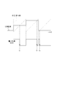
図3に示すように、S/H信号と、アナログのこぎり波と、が一致するタイミングは、量子化器212の出力信号におけるタイミングt1,t2,t3となる。量子化器212の出力信号は、デジタルのこぎり波生成部213に与えられる。生成部213は、これらのタイミングt1,t2,t3におけるデジタルのこぎり波の大きさ(デジタル値)を、アナログ入力信号のデジタル値として出力する。このデジタル値は、通信装置1が受信したRF信号(受信信号)をダウンコンバートしたデジタルIF信号となっている。なお、デジタルのこぎり波生成部213から出力される信号は、IF信号である必要はなく、ベースバンド信号であってもよい。
バンドパスΔΣ変調器214は、デジタルのこぎり波(デジタル参照信号)を入力として受け取って、アナログのこぎり波(アナログ参照信号)を信号成分として有するパルス信号を出力する。第1バンドパスフィルタ208は、ΔΣ変調器214から出力されたパルス信号に含まれる量子化雑音成分の通過を阻止し、アナログのこぎり波の信号成分を通過させるよう構成されている。第1バンドパスフィルタ208は、差分器211の一方の入力と接続されており、第1バンドパスフィルタ208の通過信号(アナログのこぎり波)を、差分器211に与えることができる。
[2.2 第2実施形態]
図4は第2実施形態に係る通信機1を示している。図1に示す通信機1は、主に、通信機1における受信機としての機能だけを示したが、図4では、通信機1における受信機及び送信機としての機能を示している。なお、第2実施形態において特に説明しない点については第1実施形態と同様である。
図4は第2実施形態に係る通信機1を示している。図1に示す通信機1は、主に、通信機1における受信機としての機能だけを示したが、図4では、通信機1における受信機及び送信機としての機能を示している。なお、第2実施形態において特に説明しない点については第1実施形態と同様である。
図4のΔΣ変調器214は、複数(3つ)の入力ポート10a,10b,10cを有している。第2実施形態のΔΣ変調器214は、複数の入力ポート10a,10b,10cから入力されたデジタル信号それぞれに対応するアナログ信号成分全てを有するパルス信号を単一の出力ポート10dから出力することができる。ΔΣ変調器214の詳細は後述する。
ΔΣ変調器214の第1入力ポート10aには、デジタルのこぎり波生成部213によって生成されたデジタルのこぎり波(第1入力信号)が入力される。同じく第2入力ポート10bには、クロック生成器217によって生成された周波数fsのクロック(第2入力信号)が入力される。同じく第3入力ポート10cには、直交変調器216によって生成されたデジタル送信信号(デジタル変調信号;デジタルRF信号)が入力される。直交変調器216は、ベースバンド信号I,Qに対するデジタル直交変調を行って、デジタル送信信号(デジタル変調信号)を生成する。なお、直交変調器216は、他の方式による変調を行う変調器であってもよい。
したがって、ΔΣ変調器214の出力ポート10dから出力されるパルス信号には、アナログのこぎり波の信号成分と、周波数fsのクロックの信号成分と、アナログ送信信号(アナログ変調信号;アナログRF信号)の信号成分と、が含まれる。
ΔΣ変調器214から出力されたパルス信号は、第1バンドパスフィルタ(第1フィルタ)208aのほか、第2バンドパスフィルタ(第2フィルタ)208b及び第3バンドパスフィルタ(第3フィルタ)208cに与えられる。第1バンドパスフィルタ208aは、図1の第1バンドパスフィルタ208と同様に、差分器211の一方の入力と接続されている。第1バンドパスフィルタ208aは、ΔΣ変調器214から出力されたパルス信号に含まれる量子化雑音成分及び他の不必要な信号成分の通過を阻止し、アナログのこぎり波の信号成分を通過させるよう構成されている。
第2バンドパスフィルタ208bは、ΔΣ変調器214から出力されたパルス信号に含まれる量子化雑音成分及び他の不必要な信号成分の通過を阻止し、周波数fsのクロック成分を通過させるよう構成されている。第2バンドパスフィルタ208bの通過信号(周波数fsのクロック)は、サンプルアンドホールド回路203のサンプリングクロックとして与えられる。
第3バンドパスフィルタ208cは、ΔΣ変調器214から出力されたパルス信号に含まれる量子化雑音成分及び他の不必要な信号成分の通過を阻止し、アナログ送信信号成分を通過させるよう構成されている。第3バンドパスフィルタ208cの通過信号(アナログ送信信号)は、アンプ209などを介して、アンテナ200から出力される。このように、アンテナ200から、デジタルのこぎり波生成部213に至る経路は、受信機としての機能を有しているのに対し、直交変調部216からアンテナ200に至る経路は送信機としての機能を有している。そして、ΔΣ変調器214は、受信機及び送信機の双方に共用されているため、回路規模の増大を抑制することができる。
また、ΔΣ変調器214からは、サンプルアンドホールド回路203のサンプリングクロックも出力することができるため、図1におけるクロック生成器204を別途設ける必要がなくなる。また、のこぎり波とサンプリングクロックとがいずれも信号処理部206によって生成されるため、図1のように信号処理部206とクロック生成器204とが分かれている場合に比べて、のこぎり波とサンプリングクロックを同期させるのが容易である。
[2.3 3入力ΔΣ変調器]
図5は、図4に示すΔΣ変調器214として用いられる3入力ΔΣ変調器214を示している。図5のΔΣ変調器214は、第1入力信号U1が入力される第1入力ポート10a、第2入力信号U2が入力される第2入力ポート10b、第3入力信号U3が入力される第3入力ポート10c、及びパルス信号を出力する単一の出力ポート10dを備えている。ΔΣ変調器214は、複数の入力ポート10a,10b,10cそれぞれに対応する複数のループフィルタ(第1ループフィルタ11、第2ループフィルタ12、第3ループフィルタ13)と、加算器15と、量子化器16と、を備えている。複数のループフィルタ11,12,13は、それぞれ、対応する入力ポート10a,10b,10cに接続された第1入力部11a,12a,13aと、フィードバック経路18a,18b,18cを介して量子化器16の出力側に接続された第2入力部11b,12b,13bと、を備えている。
図5は、図4に示すΔΣ変調器214として用いられる3入力ΔΣ変調器214を示している。図5のΔΣ変調器214は、第1入力信号U1が入力される第1入力ポート10a、第2入力信号U2が入力される第2入力ポート10b、第3入力信号U3が入力される第3入力ポート10c、及びパルス信号を出力する単一の出力ポート10dを備えている。ΔΣ変調器214は、複数の入力ポート10a,10b,10cそれぞれに対応する複数のループフィルタ(第1ループフィルタ11、第2ループフィルタ12、第3ループフィルタ13)と、加算器15と、量子化器16と、を備えている。複数のループフィルタ11,12,13は、それぞれ、対応する入力ポート10a,10b,10cに接続された第1入力部11a,12a,13aと、フィードバック経路18a,18b,18cを介して量子化器16の出力側に接続された第2入力部11b,12b,13bと、を備えている。
第1入力部11a,12a,13aには、対応する入力ポート10a,10b,10cに入力された入力信号U1,U2,U3が入力される。第2入力部11b,12b,13bには、量子化器16の出力Vのフィードバック信号Vが入力される。
複数のループフィルタ11,12,13は、それぞれ、差分器110a,120a,130aを備えている。差分器110a,120a,130aには、それぞれ、第1入力部11a,12a,13aに接続された第1経路110d,120d,130dと、第2入力部11b,12b,13bに接続された第2経路110e,120e,130eと、が接続されている。差分器110a,120a,130aは、それぞれ、入力信号U1,U2,U3と、量子化器16からのフィードバック信号Vとの差分U1-V,U2-V,U3-Vを求める。
差分器110a,120a,130aによって求められた差分U1-V,U2-V,U3-Vは、各ループフィルタ11,12,13に設けられた内部フィルタ110b,120b,130bに入力される。なお、第1ループフィルタ11の内部フィルタ110bの伝達関数をL1(z)と表現し、第2ループフィルタ12の内部フィルタ120bの伝達関数をL2(z)と表現し、第3ループフィルタ13の内部フィルタ130bの伝達関数をL3(z)と表現する。
各内部フィルタ110b,120b、130bの出力L1(z)(U1(z)-V(z)),L2(z)(U2(z)-V(z)),L3(z)(U3(z)-V(z))は、各ループフィルタ11,12,13に設けられた加算器110c,120c,130cに与えられる。各加算器110c,120c,130cには、第1入力部11a,12a,13aに入力される入力信号U1,U2,U3を加算器110c,120c,130cに入力させるためのフィードフォワード経路110f,120f,130fが接続されている。したがって、各加算器110c,120c、130cは、入力信号U1,U2,U3と、内部フィルタ110b,120b,130bの出力L1(z)(U1(z)-V(z)),L2(z)(U2(z)-V(z)),L3(z)(U3(z)-V(z))と、を加算する。
各加算器110c,120c,130cの出力(各ループフィルタ11,12,13の出力)Y1,Y2,Y3は、加算器15によって加算される。
加算器15の出力Yは、量子化器16に与えられる。本実施形態の量子化器16は、2レベル量子化器であり、1bitのパルス列を量子化信号(ΔΣ変調信号)Vとして出力する。この量子化信号VがΔΣ変調器1の出力信号となる。なお、出力信号Vは、フィードバック経路18a,18b,18cを介して各ループフィルタ11,12,13に与えられる。
図5のΔΣ変調器1の出力Vは、下記の式(1)のように表される(式(1)においてN=3の場合)。式(1)において、STFi(z)は第i入力信号Ui(z)についての第i信号伝達関数であり、NTF(z)は、ΔΣ変調器214全体での雑音伝達関数であり、E(z)は雑音伝達関数である。

ここで、




第1ループフィルタ11の内部フィルタ110bは、第1雑音伝達関数NTF1(z)を用いて示される伝達関数L1(z)を持つ。第1雑音伝達関数NTF1(z)は、第1ループフィルタ11に入力される第1入力信号(デジタルのこぎり波)U1(z)の周波数(帯域)における量子化雑音を抑制する特性(バンドストップ特性)を有するものである。
第2ループフィルタ12の内部フィルタ120bは、第2雑音伝達関数NTF2(z)を用いて示される伝達関数L2(z)を持つ。第2雑音伝達関数NTF2(z)は、第2ループフィルタ12に入力される第2入力信号(クロック)U2(z)の周波数(帯域)における量子化雑音を抑制する特性(バンドストップ特性)を有するものである。
第3ループフィルタ12の内部フィルタ130bは、第3雑音伝達関数NTF3(z)を用いて示される伝達関数L3(z)を持つ。第3雑音伝達関数NTF3(z)は、第3ループフィルタ13に入力される第3入力信号(デジタル送信信号)U3(z)の周波数(帯域)における量子化雑音を抑制する特性(バンドストップ特性)を有するものである。
第2ループフィルタ12の内部フィルタ120bは、第2雑音伝達関数NTF2(z)を用いて示される伝達関数L2(z)を持つ。第2雑音伝達関数NTF2(z)は、第2ループフィルタ12に入力される第2入力信号(クロック)U2(z)の周波数(帯域)における量子化雑音を抑制する特性(バンドストップ特性)を有するものである。
第3ループフィルタ12の内部フィルタ130bは、第3雑音伝達関数NTF3(z)を用いて示される伝達関数L3(z)を持つ。第3雑音伝達関数NTF3(z)は、第3ループフィルタ13に入力される第3入力信号(デジタル送信信号)U3(z)の周波数(帯域)における量子化雑音を抑制する特性(バンドストップ特性)を有するものである。
以上のように構成されたΔΣ変調器214は、複数の入力ポート10a,10b,10cに入力された信号を、同時に一つの単一の出力信号V(z)に含めて出力することができる。
[3.付記]
なお、今回開示された実施の形態はすべての点で例示であって制限的なものではないと考えられるべきである。本発明の範囲は、上記した意味ではなく、請求の範囲によって示され、請求の範囲と均等の意味、及び範囲内でのすべての変更が含まれることが意図される。
なお、今回開示された実施の形態はすべての点で例示であって制限的なものではないと考えられるべきである。本発明の範囲は、上記した意味ではなく、請求の範囲によって示され、請求の範囲と均等の意味、及び範囲内でのすべての変更が含まれることが意図される。
1 通信装置
10a 第1入力ポート
10b 第2入力ポート
10c 第3入力ポート
10d 出力ポート
200 アンテナ
201 ローノイズアンプ
202 バンドパスフィルタ
203 サンプルアンドホールド回路
204 クロック発生器
206 信号処理装置
207 デジタル信号処理部
208 バンドパスフィルタ
208a 第1バンドパスフィルタ
208b 第2バンドパスフィルタ
208b 第3バンドパスフィルタ
209 アンプ
211 差分器
212 量子化器
213 デジタルのこぎり波生成部
214 ΔΣ変調器
215 比較器
217 直交変調部
10a 第1入力ポート
10b 第2入力ポート
10c 第3入力ポート
10d 出力ポート
200 アンテナ
201 ローノイズアンプ
202 バンドパスフィルタ
203 サンプルアンドホールド回路
204 クロック発生器
206 信号処理装置
207 デジタル信号処理部
208 バンドパスフィルタ
208a 第1バンドパスフィルタ
208b 第2バンドパスフィルタ
208b 第3バンドパスフィルタ
209 アンプ
211 差分器
212 量子化器
213 デジタルのこぎり波生成部
214 ΔΣ変調器
215 比較器
217 直交変調部
Claims (4)
- アナログ入力信号とアナログ参照信号との比較を行う比較器と、
前記アナログ参照信号に対応するデジタル参照信号を生成するとともに、前記比較器により前記アナログ入力信号と前記アナログ参照信号との一致が検出されたときの前記デジタル参照信号の値を前記アナログ入力信号のデジタル値として出力する生成器と、
前記生成器により生成された前記デジタル参照信号をΔΣ変調するΔΣ変調器と、
前記ΔΣ変調器の出力信号のうち、前記出力信号に含まれる前記アナログ参照信号の成分を通過させるよう構成され、通過信号を前記アナログ参照信号として前記比較器に与えるよう設けられた第1フィルタと、
を備えている信号処理装置。 - 受信信号が入力されるサンプルアンドホールド回路と、
請求項1記載の信号処理装置と、
を備え、
前記サンプルアンドホール回路の出力信号が、前記アナログ入力信号として前記比較器に与えられる
通信装置。 - 前記ΔΣ変調器は、
前記デジタル参照信号が入力される第1入力ポートと、
サンプリングクロックが入力される第2入力ポートと、
第1ループフィルタと、
第2ループフィルタと、
前記第1ループフィルタ及び前記第2ループフィルタの出力を加算する加算器と、
前記加算器の出力を量子化する量子化器と、
を備え、
前記第1ループフィルタは、前記第1入力ポートに入力された前記デジタル参照信号と、前記量子化器の出力のフィードバック信号と、が入力されるように設けられ、
前記第2ループフィルタは、前記第2入力ポートに入力された前記サンプリングクロックと、前記量子化器の出力の前記フィードバック信号と、が入力されるように設けられ、
前記第1ループフィルタは、前記デジタル参照信号の周波数付近の雑音を阻止する特性を有し、
前記第2ループフィルタは、前記サンプリングクロックの周波数付近の雑音を阻止する特性を有し、
前記ΔΣ変調器の出力信号のうち、前記出力信号に含まれる前記サンプリングクロックの成分を通過させるよう構成され、通過信号をサンプリングクロックとして前記サンプルアンドホールド回路に与えるよう設けられた第2フィルタを更に備えている
請求項2記載の通信装置。 - 前記ΔΣ変調器は、
前記デジタル参照信号が入力される第1入力ポートと、
前記通信装置から送信されるアナログ送信信号に対応したデジタル送信信号が入力される第3ポートと、
第1ループフィルタと、
第3ループフィルタと、
前記第1ループフィルタ及び前記第3ループフィルタの出力を加算する加算器と、
前記加算器の出力を量子化する量子化器と、
を備え、
前記第1ループフィルタは、前記第1入力ポートに入力された前記デジタル参照信号と、前記量子化器の出力のフィードバック信号と、が入力されるよう設けられ、
前記第3ループフィルタは、前記第3ポートに入力された前記デジタル送信信号と、前記量子化器の出力のフィードバック信号と、が入力されるよう設けられ、
前記第1ループフィルタは、前記デジタル参照信号の周波数付近の雑音を阻止する特性を有し、
前記第3ループフィルタは、前記デジタル送信信号の周波数付近の雑音を阻止する特性を有し、
前記ΔΣ変調器の出力信号のうち、前記出力信号に含まれる前記アナログ送信信号の成分を通過させるよう構成された、通過信号が前記通信装置から送信される前記アナログ送信信号となるように設けられた第3フィルタを更に備えている
請求項2記載の通信装置。
Applications Claiming Priority (2)
| Application Number | Priority Date | Filing Date | Title |
|---|---|---|---|
| JP2014-096467 | 2014-05-08 | ||
| JP2014096467A JP2015216432A (ja) | 2014-05-08 | 2014-05-08 | 信号処理装置及び通信装置 |
Publications (1)
| Publication Number | Publication Date |
|---|---|
| WO2015170491A1 true WO2015170491A1 (ja) | 2015-11-12 |
Family
ID=54392345
Family Applications (1)
| Application Number | Title | Priority Date | Filing Date |
|---|---|---|---|
| PCT/JP2015/053754 Ceased WO2015170491A1 (ja) | 2014-05-08 | 2015-02-12 | 信号処理装置及び通信装置 |
Country Status (2)
| Country | Link |
|---|---|
| JP (1) | JP2015216432A (ja) |
| WO (1) | WO2015170491A1 (ja) |
Citations (2)
| Publication number | Priority date | Publication date | Assignee | Title |
|---|---|---|---|---|
| JP2000078012A (ja) * | 1998-08-07 | 2000-03-14 | Lucent Technol Inc | A/dコンバ―タ |
| JP2012005126A (ja) * | 2010-06-18 | 2012-01-05 | Foveon Inc | アナログデジタル変換用ランプ波発生器ユニット素子 |
-
2014
- 2014-05-08 JP JP2014096467A patent/JP2015216432A/ja active Pending
-
2015
- 2015-02-12 WO PCT/JP2015/053754 patent/WO2015170491A1/ja not_active Ceased
Patent Citations (2)
| Publication number | Priority date | Publication date | Assignee | Title |
|---|---|---|---|---|
| JP2000078012A (ja) * | 1998-08-07 | 2000-03-14 | Lucent Technol Inc | A/dコンバ―タ |
| JP2012005126A (ja) * | 2010-06-18 | 2012-01-05 | Foveon Inc | アナログデジタル変換用ランプ波発生器ユニット素子 |
Non-Patent Citations (1)
| Title |
|---|
| TAKASHI MAEHATA; ET AL.: "Concurrent Dual-band 1-bit Digital Transmitter Using Band-Pass Delta-Sigma Modulator", PROCEEDINGS OF THE 43RD EUROPEAN MICROWAVE CONFERENCE, 7 October 2013 (2013-10-07), pages 1523 - 1526, XP032535592 * |
Also Published As
| Publication number | Publication date |
|---|---|
| JP2015216432A (ja) | 2015-12-03 |
Similar Documents
| Publication | Publication Date | Title |
|---|---|---|
| JP5598561B2 (ja) | Δς変調器及び通信装置 | |
| CN104115406B (zh) | 连续时间的mashς‑δ模数转换 | |
| US20130271304A1 (en) | Continuous Time Analogue/Digital Converter | |
| JPH0722972A (ja) | 中間周波数デジタル受信器及び該受信器で実施されるベースバンド濾波方法 | |
| Swaminathan et al. | A digital requantizer with shaped requantization noise that remains well behaved after nonlinear distortion | |
| US8427350B2 (en) | Sigma-delta modulator | |
| CN108352847A (zh) | 用于直接取样极宽带收发器的系统和方法 | |
| CN105187068B (zh) | 一种调制电路和调制方法 | |
| TWI547842B (zh) | 觸控偵測系統、差異積分調變器及其調變方法 | |
| US20150003502A1 (en) | N-Order Noise Shaper | |
| US11799494B2 (en) | Delta-sigma modulator, delta-sigma digital-analog converter, and method for operating a delta-sigma modulator and a delta-sigma digital-analog converter | |
| Huang et al. | A simplified FRI sampling system for pulse streams based on constraint random modulation | |
| KR101593729B1 (ko) | 입력 신호로부터 rf 신호를 합성하기 위한 방법, 델타-시그마 변조기 및 집적 회로 | |
| JP4901112B2 (ja) | 帯域デルタ−シグマ・アナログ−デジタル変換器 | |
| JPH10107639A (ja) | アナログ/デジタル変換装置 | |
| JP2015216432A (ja) | 信号処理装置及び通信装置 | |
| TWI477086B (zh) | 雙模態δ-△類比至數位轉換器與其電路 | |
| US9362943B2 (en) | Converter | |
| JP2014225922A (ja) | Δς変調器及び通信装置 | |
| US20060214829A1 (en) | Sigma delta analog-to-digital converter | |
| JP6623914B2 (ja) | 送信システム、送信装置、及び通信システム | |
| JP2010187298A (ja) | バンドパス・デルタシグマa/d変換器 | |
| JP3438018B2 (ja) | A/d変換装置及びd/a変換装置 | |
| JP6627019B2 (ja) | 信号変換装置 | |
| CN101120507A (zh) | 一种ad转换器装置 |
Legal Events
| Date | Code | Title | Description |
|---|---|---|---|
| 121 | Ep: the epo has been informed by wipo that ep was designated in this application |
Ref document number: 15788868 Country of ref document: EP Kind code of ref document: A1 |
|
| NENP | Non-entry into the national phase |
Ref country code: DE |
|
| 122 | Ep: pct application non-entry in european phase |
Ref document number: 15788868 Country of ref document: EP Kind code of ref document: A1 |