WO2015162986A1 - 円筒型スパッタリングターゲット用素材 - Google Patents
円筒型スパッタリングターゲット用素材 Download PDFInfo
- Publication number
- WO2015162986A1 WO2015162986A1 PCT/JP2015/054770 JP2015054770W WO2015162986A1 WO 2015162986 A1 WO2015162986 A1 WO 2015162986A1 JP 2015054770 W JP2015054770 W JP 2015054770W WO 2015162986 A1 WO2015162986 A1 WO 2015162986A1
- Authority
- WO
- WIPO (PCT)
- Prior art keywords
- grain boundary
- sputtering target
- outer peripheral
- boundary length
- peripheral surface
- Prior art date
- Legal status (The legal status is an assumption and is not a legal conclusion. Google has not performed a legal analysis and makes no representation as to the accuracy of the status listed.)
- Ceased
Links
Images


Classifications
-
- H—ELECTRICITY
- H01—ELECTRIC ELEMENTS
- H01J—ELECTRIC DISCHARGE TUBES OR DISCHARGE LAMPS
- H01J37/00—Discharge tubes with provision for introducing objects or material to be exposed to the discharge, e.g. for the purpose of examination or processing thereof
- H01J37/32—Gas-filled discharge tubes
- H01J37/34—Gas-filled discharge tubes operating with cathodic sputtering
- H01J37/3411—Constructional aspects of the reactor
- H01J37/3414—Targets
- H01J37/3426—Material
-
- C—CHEMISTRY; METALLURGY
- C23—COATING METALLIC MATERIAL; COATING MATERIAL WITH METALLIC MATERIAL; CHEMICAL SURFACE TREATMENT; DIFFUSION TREATMENT OF METALLIC MATERIAL; COATING BY VACUUM EVAPORATION, BY SPUTTERING, BY ION IMPLANTATION OR BY CHEMICAL VAPOUR DEPOSITION, IN GENERAL; INHIBITING CORROSION OF METALLIC MATERIAL OR INCRUSTATION IN GENERAL
- C23C—COATING METALLIC MATERIAL; COATING MATERIAL WITH METALLIC MATERIAL; SURFACE TREATMENT OF METALLIC MATERIAL BY DIFFUSION INTO THE SURFACE, BY CHEMICAL CONVERSION OR SUBSTITUTION; COATING BY VACUUM EVAPORATION, BY SPUTTERING, BY ION IMPLANTATION OR BY CHEMICAL VAPOUR DEPOSITION, IN GENERAL
- C23C14/00—Coating by vacuum evaporation, by sputtering or by ion implantation of the coating forming material
- C23C14/22—Coating by vacuum evaporation, by sputtering or by ion implantation of the coating forming material characterised by the process of coating
- C23C14/34—Sputtering
- C23C14/3407—Cathode assembly for sputtering apparatus, e.g. Target
-
- C—CHEMISTRY; METALLURGY
- C22—METALLURGY; FERROUS OR NON-FERROUS ALLOYS; TREATMENT OF ALLOYS OR NON-FERROUS METALS
- C22C—ALLOYS
- C22C9/00—Alloys based on copper
-
- C—CHEMISTRY; METALLURGY
- C22—METALLURGY; FERROUS OR NON-FERROUS ALLOYS; TREATMENT OF ALLOYS OR NON-FERROUS METALS
- C22C—ALLOYS
- C22C9/00—Alloys based on copper
- C22C9/01—Alloys based on copper with aluminium as the next major constituent
-
- C—CHEMISTRY; METALLURGY
- C22—METALLURGY; FERROUS OR NON-FERROUS ALLOYS; TREATMENT OF ALLOYS OR NON-FERROUS METALS
- C22C—ALLOYS
- C22C9/00—Alloys based on copper
- C22C9/05—Alloys based on copper with manganese as the next major constituent
-
- C—CHEMISTRY; METALLURGY
- C22—METALLURGY; FERROUS OR NON-FERROUS ALLOYS; TREATMENT OF ALLOYS OR NON-FERROUS METALS
- C22F—CHANGING THE PHYSICAL STRUCTURE OF NON-FERROUS METALS AND NON-FERROUS ALLOYS
- C22F1/00—Changing the physical structure of non-ferrous metals or alloys by heat treatment or by hot or cold working
- C22F1/08—Changing the physical structure of non-ferrous metals or alloys by heat treatment or by hot or cold working of copper or alloys based thereon
-
- C—CHEMISTRY; METALLURGY
- C23—COATING METALLIC MATERIAL; COATING MATERIAL WITH METALLIC MATERIAL; CHEMICAL SURFACE TREATMENT; DIFFUSION TREATMENT OF METALLIC MATERIAL; COATING BY VACUUM EVAPORATION, BY SPUTTERING, BY ION IMPLANTATION OR BY CHEMICAL VAPOUR DEPOSITION, IN GENERAL; INHIBITING CORROSION OF METALLIC MATERIAL OR INCRUSTATION IN GENERAL
- C23C—COATING METALLIC MATERIAL; COATING MATERIAL WITH METALLIC MATERIAL; SURFACE TREATMENT OF METALLIC MATERIAL BY DIFFUSION INTO THE SURFACE, BY CHEMICAL CONVERSION OR SUBSTITUTION; COATING BY VACUUM EVAPORATION, BY SPUTTERING, BY ION IMPLANTATION OR BY CHEMICAL VAPOUR DEPOSITION, IN GENERAL
- C23C14/00—Coating by vacuum evaporation, by sputtering or by ion implantation of the coating forming material
- C23C14/0021—Reactive sputtering or evaporation
- C23C14/0036—Reactive sputtering
-
- C—CHEMISTRY; METALLURGY
- C23—COATING METALLIC MATERIAL; COATING MATERIAL WITH METALLIC MATERIAL; CHEMICAL SURFACE TREATMENT; DIFFUSION TREATMENT OF METALLIC MATERIAL; COATING BY VACUUM EVAPORATION, BY SPUTTERING, BY ION IMPLANTATION OR BY CHEMICAL VAPOUR DEPOSITION, IN GENERAL; INHIBITING CORROSION OF METALLIC MATERIAL OR INCRUSTATION IN GENERAL
- C23C—COATING METALLIC MATERIAL; COATING MATERIAL WITH METALLIC MATERIAL; SURFACE TREATMENT OF METALLIC MATERIAL BY DIFFUSION INTO THE SURFACE, BY CHEMICAL CONVERSION OR SUBSTITUTION; COATING BY VACUUM EVAPORATION, BY SPUTTERING, BY ION IMPLANTATION OR BY CHEMICAL VAPOUR DEPOSITION, IN GENERAL
- C23C14/00—Coating by vacuum evaporation, by sputtering or by ion implantation of the coating forming material
- C23C14/06—Coating by vacuum evaporation, by sputtering or by ion implantation of the coating forming material characterised by the coating material
- C23C14/08—Oxides
- C23C14/087—Oxides of copper or solid solutions thereof
-
- C—CHEMISTRY; METALLURGY
- C23—COATING METALLIC MATERIAL; COATING MATERIAL WITH METALLIC MATERIAL; CHEMICAL SURFACE TREATMENT; DIFFUSION TREATMENT OF METALLIC MATERIAL; COATING BY VACUUM EVAPORATION, BY SPUTTERING, BY ION IMPLANTATION OR BY CHEMICAL VAPOUR DEPOSITION, IN GENERAL; INHIBITING CORROSION OF METALLIC MATERIAL OR INCRUSTATION IN GENERAL
- C23C—COATING METALLIC MATERIAL; COATING MATERIAL WITH METALLIC MATERIAL; SURFACE TREATMENT OF METALLIC MATERIAL BY DIFFUSION INTO THE SURFACE, BY CHEMICAL CONVERSION OR SUBSTITUTION; COATING BY VACUUM EVAPORATION, BY SPUTTERING, BY ION IMPLANTATION OR BY CHEMICAL VAPOUR DEPOSITION, IN GENERAL
- C23C14/00—Coating by vacuum evaporation, by sputtering or by ion implantation of the coating forming material
- C23C14/06—Coating by vacuum evaporation, by sputtering or by ion implantation of the coating forming material characterised by the coating material
- C23C14/14—Metallic material, boron or silicon
-
- C—CHEMISTRY; METALLURGY
- C23—COATING METALLIC MATERIAL; COATING MATERIAL WITH METALLIC MATERIAL; CHEMICAL SURFACE TREATMENT; DIFFUSION TREATMENT OF METALLIC MATERIAL; COATING BY VACUUM EVAPORATION, BY SPUTTERING, BY ION IMPLANTATION OR BY CHEMICAL VAPOUR DEPOSITION, IN GENERAL; INHIBITING CORROSION OF METALLIC MATERIAL OR INCRUSTATION IN GENERAL
- C23C—COATING METALLIC MATERIAL; COATING MATERIAL WITH METALLIC MATERIAL; SURFACE TREATMENT OF METALLIC MATERIAL BY DIFFUSION INTO THE SURFACE, BY CHEMICAL CONVERSION OR SUBSTITUTION; COATING BY VACUUM EVAPORATION, BY SPUTTERING, BY ION IMPLANTATION OR BY CHEMICAL VAPOUR DEPOSITION, IN GENERAL
- C23C14/00—Coating by vacuum evaporation, by sputtering or by ion implantation of the coating forming material
- C23C14/22—Coating by vacuum evaporation, by sputtering or by ion implantation of the coating forming material characterised by the process of coating
- C23C14/34—Sputtering
-
- C—CHEMISTRY; METALLURGY
- C23—COATING METALLIC MATERIAL; COATING MATERIAL WITH METALLIC MATERIAL; CHEMICAL SURFACE TREATMENT; DIFFUSION TREATMENT OF METALLIC MATERIAL; COATING BY VACUUM EVAPORATION, BY SPUTTERING, BY ION IMPLANTATION OR BY CHEMICAL VAPOUR DEPOSITION, IN GENERAL; INHIBITING CORROSION OF METALLIC MATERIAL OR INCRUSTATION IN GENERAL
- C23C—COATING METALLIC MATERIAL; COATING MATERIAL WITH METALLIC MATERIAL; SURFACE TREATMENT OF METALLIC MATERIAL BY DIFFUSION INTO THE SURFACE, BY CHEMICAL CONVERSION OR SUBSTITUTION; COATING BY VACUUM EVAPORATION, BY SPUTTERING, BY ION IMPLANTATION OR BY CHEMICAL VAPOUR DEPOSITION, IN GENERAL
- C23C14/00—Coating by vacuum evaporation, by sputtering or by ion implantation of the coating forming material
- C23C14/22—Coating by vacuum evaporation, by sputtering or by ion implantation of the coating forming material characterised by the process of coating
- C23C14/34—Sputtering
- C23C14/3407—Cathode assembly for sputtering apparatus, e.g. Target
- C23C14/3414—Metallurgical or chemical aspects of target preparation, e.g. casting, powder metallurgy
-
- H—ELECTRICITY
- H01—ELECTRIC ELEMENTS
- H01J—ELECTRIC DISCHARGE TUBES OR DISCHARGE LAMPS
- H01J37/00—Discharge tubes with provision for introducing objects or material to be exposed to the discharge, e.g. for the purpose of examination or processing thereof
- H01J37/32—Gas-filled discharge tubes
- H01J37/34—Gas-filled discharge tubes operating with cathodic sputtering
- H01J37/3411—Constructional aspects of the reactor
- H01J37/3414—Targets
- H01J37/342—Hollow targets
-
- H—ELECTRICITY
- H01—ELECTRIC ELEMENTS
- H01J—ELECTRIC DISCHARGE TUBES OR DISCHARGE LAMPS
- H01J37/00—Discharge tubes with provision for introducing objects or material to be exposed to the discharge, e.g. for the purpose of examination or processing thereof
- H01J37/32—Gas-filled discharge tubes
- H01J37/34—Gas-filled discharge tubes operating with cathodic sputtering
- H01J37/3411—Constructional aspects of the reactor
- H01J37/3414—Targets
- H01J37/3423—Shape
-
- H—ELECTRICITY
- H10—SEMICONDUCTOR DEVICES; ELECTRIC SOLID-STATE DEVICES NOT OTHERWISE PROVIDED FOR
- H10P—GENERIC PROCESSES OR APPARATUS FOR THE MANUFACTURE OR TREATMENT OF DEVICES COVERED BY CLASS H10
- H10P14/00—Formation of materials, e.g. in the shape of layers or pillars
- H10P14/40—Formation of materials, e.g. in the shape of layers or pillars of conductive or resistive materials
- H10P14/42—Formation of materials, e.g. in the shape of layers or pillars of conductive or resistive materials using a gas or vapour
-
- C—CHEMISTRY; METALLURGY
- C22—METALLURGY; FERROUS OR NON-FERROUS ALLOYS; TREATMENT OF ALLOYS OR NON-FERROUS METALS
- C22C—ALLOYS
- C22C9/00—Alloys based on copper
- C22C9/02—Alloys based on copper with tin as the next major constituent
-
- C—CHEMISTRY; METALLURGY
- C22—METALLURGY; FERROUS OR NON-FERROUS ALLOYS; TREATMENT OF ALLOYS OR NON-FERROUS METALS
- C22C—ALLOYS
- C22C9/00—Alloys based on copper
- C22C9/04—Alloys based on copper with zinc as the next major constituent
-
- C—CHEMISTRY; METALLURGY
- C22—METALLURGY; FERROUS OR NON-FERROUS ALLOYS; TREATMENT OF ALLOYS OR NON-FERROUS METALS
- C22C—ALLOYS
- C22C9/00—Alloys based on copper
- C22C9/06—Alloys based on copper with nickel or cobalt as the next major constituent
-
- C—CHEMISTRY; METALLURGY
- C22—METALLURGY; FERROUS OR NON-FERROUS ALLOYS; TREATMENT OF ALLOYS OR NON-FERROUS METALS
- C22F—CHANGING THE PHYSICAL STRUCTURE OF NON-FERROUS METALS AND NON-FERROUS ALLOYS
- C22F1/00—Changing the physical structure of non-ferrous metals or alloys by heat treatment or by hot or cold working
Definitions
- the present invention relates to a material for a cylindrical sputtering target, which is a material for a cylindrical sputtering target for sputtering a thin film made of copper or a copper alloy.
- Al or an Al alloy is widely used as a flat panel display such as a liquid crystal or an organic EL panel, or a wiring film such as a touch panel.
- miniaturization (narrowing) and thinning of the wiring film have been attempted, and a wiring film having a lower specific resistance than before has been demanded. Accordingly, with the miniaturization and thinning of the wiring film described above, a wiring film using copper or a copper alloy, which is a material having a lower specific resistance than Al or an Al alloy, is provided.
- a sputtering method using a sputtering target is usually applied.
- a sputtering target for example, a flat plate sputtering target as shown in Patent Document 1 and a cylindrical sputtering target as shown in Patent Document 2 have been proposed.
- the outer surface of the cylindrical sputtering target is a sputtering surface and sputtering is performed while rotating the target, it is suitable for continuous film formation as compared with the case of using a flat plate sputtering target. And it has the advantage that it is excellent in the use efficiency of a target.
- abnormal discharge when film formation is performed using a sputtering target, abnormal discharge (arcing) may occur due to foreign matter in the sputtering target, and thus a uniform wiring film may not be formed.
- abnormal discharge is a phenomenon in which an extremely high current suddenly and suddenly flows compared to that during normal sputtering, and an abnormally large discharge occurs suddenly. This may cause generation of particles and / or non-uniform thickness of the wiring film. Therefore, it is desirable to avoid as much as possible abnormal discharge during film formation.
- the present invention has been made in view of the above-described circumstances, and provides a material for a cylindrical sputtering target that is made of copper or a copper alloy and can stably form a film while suppressing the occurrence of abnormal discharge.
- the purpose is to do.
- a material for a cylindrical sputtering target according to an aspect of the present invention is a material for a cylindrical sputtering target made of copper or a copper alloy, and the grain boundary in the measurement range is measured by the EBSD method.
- the outer peripheral surface and the central part of both end portions in the axial direction are defined as The average value of the special grain boundary length ratio L ⁇ N / L N measured on the outer peripheral surface is set to 0.5 or more, and the special grain boundary is measured on the outer peripheral surface of both ends in the axial direction and the outer peripheral surface of the central portion.
- the average value of the above-mentioned special grain boundary length ratio L ⁇ N / L N is 0.5 or more in the crystal structure of the outer peripheral surface.
- each value of the special grain boundary length ratio L ⁇ N / L N measured on the outer peripheral surface of both end portions in the axial direction and the outer peripheral surface of the central portion is within ⁇ 20% of the average value. It is said that.
- the boundary of the crystal grain boundary is improved on the outer peripheral surface that becomes the sputter surface, and the entire sputter surface is sputtered uniformly, and the occurrence of abnormal discharge can be suppressed even during sputtering under high output. it can.
- the total content of impurity elements Si and C is 10 mass ppm or less, O content is 50 mass ppm or less, Abnormal discharge due to these impurities can be suppressed.
- the average crystal grain size is in the range of 10 ⁇ m or more and 150 ⁇ m or less in the crystal structure of the outer peripheral surface.
- the average crystal grain size on the outer peripheral surface is relatively fine such as 10 ⁇ m or more and 150 ⁇ m or less, the crystal grain size on the sputter surface becomes fine and it becomes possible to carry out the sputtering stably. The occurrence of discharge can be suppressed.
- the area ratio occupied by crystal grains twice as large as the average crystal grain size is less than 20% of the total crystal area. It is preferable that In this case, since the crystal grain size of the outer peripheral surface serving as the sputtering surface is uniform, sputtering is performed uniformly over the entire sputtering surface, and the occurrence of abnormal discharge can be reliably suppressed.
- a cylindrical sputtering target material that is made of copper or a copper alloy and that can stably form a film while suppressing the occurrence of abnormal discharge.
- the cylindrical sputtering target material 10 is a material for a cylindrical sputtering target used when a thin film (wiring film) made of copper or a copper alloy is formed on a glass substrate or the like by sputtering.
- the cylindrical sputtering target material 10 has a cylindrical shape.
- the outer diameter D is in the range of 140 mm ⁇ D ⁇ 180 mm
- the inner diameter d is in the range of 110 mm ⁇ d ⁇ 135 mm.
- the axial length L is in the range of 1000 mm ⁇ L ⁇ 4000 mm.
- the outer peripheral surface 11 of the cylindrical sputtering target material 10 is a sputtering surface in the cylindrical sputtering target.
- the cylindrical sputtering target material 10 is made of copper or a copper alloy having a composition corresponding to a thin film made of copper or a copper alloy.
- the cylindrical sputtering target material 10 according to this embodiment has a total content of Si and C, which are impurity elements, of 10 mass ppm or less and an O content of 50 mass ppm or less.
- pure copper such as oxygen-free copper, or Mg, Al, Ag, Ti, Zr, Mn, Ca, Cr, Sn, Ni, Zn, Co , P is made of a copper alloy containing one or more selected from P.
- the content is A total range of 0.001% by mass to 10% by mass is desirable.
- the lower limit of the total content of Si and C may be 0.01 mass ppm, and the lower limit of the O content may be 0.5 mass ppm.
- the total content of Si and C is preferably 0.01 mass ppm or more and 2 mass ppm or less, and the O content is preferably 0.5 mass ppm or more and 10 mass ppm or less. It is not limited to.
- examples of the copper alloy constituting the cylindrical sputtering target material 10 include Cu-0.002 to 2 mass% Mg alloy, Cu-0.001 to 10 mass% Al alloy, Cu-0.
- examples include 001 to 10 mass% Mn alloy, Cu-0.05 to 4 mass% Ca alloy, Cu-0.01 to 10 mass% Ag alloy.
- the total grain boundary length L of the grain boundary in the measurement range is measured by the EBSD method in the crystal structure of the outer peripheral surface serving as the sputtering surface.
- the unit total grain boundary length L N in terms of unit area 1 mm 2 per a further measure total special grain boundary length L ⁇ special grain boundaries in the measurement range, units total which was converted to the unit area 1 mm 2 per
- the special grain boundary length L ⁇ N and the special grain boundary length ratio L ⁇ N / L N defined by the above-mentioned special grain boundary measured by measuring the outer peripheral surface at both ends in the axis O direction and the outer peripheral surface at the central portion.
- the average value of the length ratio L ⁇ N / L N is 0.5 or more.
- the upper limit of the average value of the special grain boundary length ratio L ⁇ N / L N may be 1.
- the EBSD method means an electron beam diffraction diffraction pattern (EBSD) method using a scanning electron microscope with a backscattered electron diffraction image system.
- OIM is data analysis software (OIM) for analyzing crystal orientation using measurement data obtained by EBSD.
- the CI value is a reliability index, which is displayed as a numerical value representing the reliability of crystal orientation determination when analyzed using the analysis software OIM Analysis (Ver. 5.3) of the EBSD device.
- OIM data analysis software
- the special grain boundary is a ⁇ value defined crystallographically based on CSL theory (Kronberg et al: Trans. Met. Soc. AIME, 185, 501 (1949)) and corresponding to 3 ⁇ ⁇ ⁇ 29.
- the grain boundary and the inherent corresponding site lattice orientation defect Dq at the corresponding grain boundary is Dq ⁇ 15 ° / ⁇ 1/2 (DG Brandon: Acta. Metallurgica. Vol. 14, p. 1479, (1966)).
- a crystal grain boundary is defined as a boundary between crystals when the orientation difference between two adjacent crystals is 15 ° or more as a result of two-dimensional cross-sectional observation.
- each value of the special grain boundary length ratio L ⁇ N / L N measured on the outer peripheral surface at both ends of the axis O direction and the outer peripheral surface of the central portion. Is within a range of ⁇ 20% with respect to the average value of the measured special grain boundary length ratio L ⁇ N / L N.
- Each value of the axis O direction end portions of the outer peripheral surface and the central portion of the outer peripheral surface at the measured special grain boundary length ratio L ⁇ N / L N is, the special grain boundaries were measured length ratio L ⁇ N / L N
- the average value is preferably within a range of ⁇ 10%, but is not limited thereto. In the present embodiment, as shown in FIG.
- 4 points (a1, a2, a3, a4), four points (b1, b2, b3, b4) at 90 ° intervals in the circumferential direction at the center of the axis O direction, and the end face on the other side in the axis O direction
- the average crystal grain size is in the range of 10 ⁇ m or more and 150 ⁇ m or less in the crystal structure of the outer peripheral surface.
- the average crystal grain size is calculated by calculating the number of crystal grains in the observation area from the crystal grain boundary specified by the above-mentioned EBSD method, and dividing the total length of the crystal grain boundary in the observation area by the number of crystal grains. It calculated
- the average crystal grain size is preferably 20 ⁇ m or more and 100 ⁇ m or less, but is not limited thereto.
- the area ratio occupied by crystal grains twice or more the average crystal grain size is less than 20% of the total crystal area.
- the area ratio occupied by crystal grains twice or more the average crystal grain size after calculating the average crystal grain size, a crystal grain twice or more the average crystal grain size is specified, and the crystal Count the grain size and number, calculate the area occupied by the crystal grain more than twice the average grain size, and count the crystal grain size and number of all the observed crystal grains. Obtained by calculating.
- the lower limit of the area ratio occupied by crystal grains twice or more the average crystal grain size may be 5%.
- the area ratio occupied by the crystal grains twice or more the average crystal grain size is preferably 5% or more and 15% or less, but is not limited thereto.
- a casting step S01 for casting an ingot a hot working step S02 for producing a cylindrical hot-worked material by performing hot working on the ingot, and the obtained cylindrical heat
- a cold working step S03 for performing cold working on the cold-worked material and a heat treatment step S04 for carrying out heat treatment on the cylindrical work material subjected to the cold working step S03.
- the cold working step S03 and the heat treatment step S04 are repeatedly performed.
- the cylindrical hot work material and the cylindrical hot work material are cold-worked. Cold processing is performed on the cylindrical processed material that has been processed and heat-treated.
- a cylindrical ingot is continuously produced and cut into a predetermined length using various casting machines such as a vertical continuous casting machine, a horizontal continuous casting machine, and a semi-continuous casting machine.
- the Si content is ⁇ 10 mass ppm and the C content is ⁇ 5 mass so that the total content of impurity elements Si and C is 10 mass ppm or less.
- melt casting is performed at 1200 ° C. or less, which is a temperature at which Si does not elute from the furnace material or the like.
- the furnace atmosphere during preheating, melting, and holding of a melting raw material such as electrolytic copper is controlled so as to be CO: 0.5 to 5.0 vol%, and the molten copper passes through
- a non-oxidizing atmosphere By sealing in a non-oxidizing atmosphere, it becomes possible to produce an ingot of O ⁇ 50 mass ppm without increasing oxygen in the subsequent process in a state in which oxygen is reduced to the limit when electrolytic copper is dissolved.
- the alloy element addition is performed in the controlled atmosphere described above.
- the cylindrical ingot is heated to the recrystallization temperature or higher and subjected to rolling or extrusion to produce a cylindrical hot work material.
- a cylindrical hot-work material is manufactured by hot extrusion.
- the average crystal grain size of the above-described cylindrical hot-worked material is preferably targeted for the crystal structure of the outer peripheral surface serving as the sputtering surface in the cylindrical sputtering target.
- the lower limit value of the average crystal grain size of the cylindrical hot-worked material may be 0.01 mm.
- the average crystal grain size of the cylindrical hot-worked material is more preferably 0.01 mm or more and 0.3 mm or less, but is not limited thereto.
- the cold working step S03 cold working is performed on the cylindrical ingot (and the cylindrical work material obtained by subjecting the cylindrical ingot to cold working and heat treatment).
- the pipe expanding step for expanding the outer diameter of the cylindrical ingot or the cylindrical workpiece before the cold working is performed at least twice or more by drawing. is doing.
- heat treatment is performed on the cylindrical workpiece that has been cold worked.
- the heat treatment means is not particularly limited, and a batch type heat treatment furnace, a continuous annealing furnace, or the like can be applied.
- the heat treatment step S04 is performed using a batch-type heat treatment furnace. Within the following range.
- the total reduction of the thickness degree of work is 15 to 25%, the outer diameter expansion is 30% or less, and the inner diameter expansion.
- the condition of the cold working step S03 is set so that the value is 20% or less.
- the cylindrical sputtering target material 10 formed as described above is further processed and used as a cylindrical sputtering target.
- the cylindrical sputtering target is used while being rotated around the axis line in the sputtering apparatus, and its outer peripheral surface is used as a sputtering surface.
- the total content of impurity elements Si and C is 10 mass ppm or less, and the O content is 50 mass ppm. In the following description, abnormal discharge caused by these impurities can be suppressed.
- the average value of the special grain boundary length ratio L ⁇ N / L N measured on the other side (c1, c2, c3, c4) in the axis O direction is set to 0.5 or more, and each measurement The value is within a range of ⁇ 20% with respect to the average value of the special grain boundary length ratio L ⁇ N / L N.
- the boundary of the crystal grain boundary is improved on the outer peripheral surface that becomes the sputter surface, and the entire sputter surface is sputtered uniformly, and the occurrence of abnormal discharge can be suppressed even during sputtering under high output. it can.
- the average crystal grain size on the outer peripheral surface is within the range of 10 ⁇ m or more and 150 ⁇ m or less, and the crystal is twice or more the average crystal grain size.
- the area ratio occupied by the grains is less than 20% of the total crystal area. Therefore, the crystal structure of the outer peripheral surface is uniformly refined, and sputtering can be performed uniformly over the entire sputtering surface, and the occurrence of abnormal discharge can be reliably suppressed.
- cylindrical sputtering target material 10 of the present embodiment 1 selected from Mg, Al, Ag, Ti, Zr, Mn, Ca, Cr, Sn, Ni, Zn, Co, and P Since a copper alloy containing seeds or two or more kinds is used, a cylindrical sputtering target material 10 capable of forming a thin film excellent in various properties such as resistivity, heat resistance, and corrosion resistance can be obtained. .
- the content of one or more selected from Mg, Al, Ag, Ti, Zr, Mn, Ca, Cr, Sn, Ni, Zn, Co, and P is It is desirable that the total amount be in the range of 0.001% by mass or more and 10% by mass or less.
- the average crystal grain size on the outer peripheral surface of the cylindrical hot work material is set to 20 ⁇ m or less, the cold work and heat treatment are repeatedly performed on the cylindrical hot work material. By carrying out, it becomes possible to obtain the cylindrical sputtering target material 10 in which the crystal structure of the outer peripheral surface is uniformly refined.
- each of the value of the special grain boundary length ratio L ⁇ N / L N is the mean value of all the measured special grain boundary length ratio L ⁇ N / L N Can be within a range of ⁇ 20%.
- the conditions of the heat treatment step S03 are described as the heat treatment temperature: 400 ° C. or more and 900 ° C. or less, and the holding time within the heat treatment temperature range: 15 minutes or more and 120 minutes or less.
- the heat treatment conditions may be appropriately set according to the composition and size of the cylindrical sputtering target material to be formed, the heat treatment apparatus, and the like.
- pure copper such as oxygen-free copper, Mg, Al, Ag, Ti, Zr, Mn, Ca, Cr, Sn, Ni, as the copper or copper alloy constituting the cylindrical sputtering target material 10
- oxygen-free copper Mg, Al, Ag, Ti, Zr, Mn, Ca, Cr, Sn, Ni
- copper or copper alloy constituting the cylindrical sputtering target material 10
- the description has been given by taking as an example a copper alloy containing one or more selected from Zn, Co, and P, with the balance being copper and inevitable impurities, but other copper or copper Alloys may be targeted.
- a cylindrical ingot is manufactured by a continuous casting step S11 using a continuous casting machine or a semi-continuous casting machine, and cold processing is performed on the cylindrical ingot. It is good also as a structure which repeatedly performs cold processing process S13 to perform and heat processing process S14 which performs heat processing with respect to the cylindrical workpiece which performed cold processing process S13.
- the continuous casting step S11 it is preferable to set the casting conditions so that the average crystal grain size of the obtained cylindrical ingot is 20 mm or less.
- the average crystal grain size of the cylindrical ingot is preferably the crystal structure of the outer peripheral surface that becomes the sputtering surface in the cylindrical sputtering target.
- the furnace atmosphere during preheating, melting, and holding of a melting raw material such as electrolytic copper is controlled to be CO: 0.5 to 5.0 vol%.
- the inside was a non-oxidizing atmosphere or a reducing atmosphere.
- the ingot was heated to 800 ° C. and subjected to hot extrusion to produce a cylindrical hot work material (outer diameter 150 mm, inner diameter 80 mm).
- the obtained cylindrical hot-worked material is repeatedly subjected to drawing processing (1 to 10 passes) and heat treatment (400 to 800 ° C. ⁇ 15 minutes to 120 minutes) in order, and correction processing is performed, and the outer diameter is 174 mm.
- a material for a cylindrical sputtering target having an inner diameter of 118 mm was obtained.
- the cylindrical sputtering target was manufactured using this raw material for cylindrical sputtering targets. The following evaluation was implemented about the above-mentioned raw material for cylindrical sputtering targets and a cylindrical sputtering target.
- ⁇ Analysis of impurity elements The content of Si in the cylindrical sputtering target material was measured by solid-state emission spectroscopy using ARL-4460 manufactured by TFS. The content of C in the cylindrical sputtering target material was measured by a combustion-infrared absorption method using a CSLS 600 manufactured by LECO. The content of O in the cylindrical sputtering target material was measured by an inert gas melting-infrared absorption method (JIS H 1067) using RO-600 manufactured by LECO.
- JIS H 1067 inert gas melting-infrared absorption method
- each sample was mechanically polished using water-resistant abrasive paper and diamond abrasive grains, and then final polished using a colloidal silica solution. Then, by using an EBSD measuring device (HITACHI S4300-SEM, EDAX / TSL OIM Data Collection) and analysis software (EDAX / TSL OIM Data Analysis ver. 5.2), grain boundaries and special grain boundaries The specific grain boundary length ratio was analyzed by specifying the length and calculating the length.
- HITACHI S4300-SEM EDAX / TSL OIM Data Collection
- analysis software EDAX / TSL OIM Data Analysis ver. 5.2
- each measurement point (pixel) within the measurement range of the sample surface is irradiated with an electron beam, the electron beam is scanned two-dimensionally on the sample surface, and the orientation by backscattered electron diffraction
- the measurement point where the orientation difference between adjacent measurement points is 15 ° or more was identified as a grain boundary.
- the total grain boundary length L of the crystal grain boundaries in the measurement range was measured, and the unit total grain boundary length L N was calculated by converting this to a unit area of 1 mm 2 .
- the position of the crystal grain boundary where the interface between adjacent crystal grains constitutes the special grain boundary is determined and the total special grain boundary length L ⁇ of the special grain boundary is measured, and this is converted into a unit per 1 mm 2 unit area. to determine the total special grain boundary length L ⁇ N. Further, a special grain boundary length ratio (L ⁇ N / L N ), which is a ratio between the unit total grain boundary length L N and the unit total special grain boundary length L ⁇ N , was calculated. Then, it calculates the average value from all measured special grain boundary length ratio L ⁇ N / L N, the maximum variation with respect to the average value of the measured values of the special grain boundary length ratio L ⁇ N / L N evaluated.
- ⁇ Average crystal grain size of cylindrical sputtering target material The crystal structure on the outer peripheral surface of the obtained cylindrical sputtering target material was observed, and the average crystal grain size was calculated.
- an EBSD measurement apparatus S4300-SE manufactured by HITACHI, OIM Data Collection manufactured by EDAX / TSL
- EDAX analysis software
- the grain boundaries were identified by OIM Data Analysis ver. Measurement conditions are: measurement range: 680 ⁇ 1020 ⁇ m / measurement step: 2.0 ⁇ m / take-in time: 20 msec. / Point.
- each measurement point (pixel) within the measurement range on the sample surface is irradiated with an electron beam, and the adjacent measurement is performed by orientation analysis using the backscattered electron beam analysis method.
- the measurement point where the orientation difference between the points was 15 ° or more was defined as a grain boundary. From the obtained crystal grain boundary, calculate the number of crystal grains in the observation area, calculate the crystal grain area by dividing the total length of the crystal grain boundary in the observation area by the number of crystal grains, and by converting it into a circle, The average grain size was taken.
- the boundary of the crystal grain boundary is improved on the outer peripheral surface serving as a sputtering surface, and the entire sputtering surface is sputtered uniformly. Also, the occurrence of abnormal discharge can be suppressed. Moreover, according to the cylindrical sputtering target material of the present invention, it is possible to suppress abnormal discharge caused by impurities and stably form a film.
Landscapes
- Chemical & Material Sciences (AREA)
- Engineering & Computer Science (AREA)
- Mechanical Engineering (AREA)
- Materials Engineering (AREA)
- Metallurgy (AREA)
- Organic Chemistry (AREA)
- Chemical Kinetics & Catalysis (AREA)
- Physics & Mathematics (AREA)
- Plasma & Fusion (AREA)
- Analytical Chemistry (AREA)
- Thermal Sciences (AREA)
- Crystallography & Structural Chemistry (AREA)
- Physical Vapour Deposition (AREA)
- Electrodes Of Semiconductors (AREA)
Abstract
Description
本願は、2014年4月22日に、日本に出願された特願2014-088186号に基づき優先権を主張し、その内容をここに援用する。
そこで、上述の配線膜の微細化および薄膜化にともない、Al又はAl合金よりも比抵抗の低い材料である銅又は銅合金を用いた配線膜が提供されている。
上述のスパッタリングターゲットとしては、例えば特許文献1に示すような平板型スパッタリングターゲットや、特許文献2に示すような円筒型スパッタリングターゲットが提案されている。
さらに、本発明の円筒型スパッタリングターゲット用素材によれば、不純物元素であるSiとCとの含有量の総計が10質量ppm以下、O含有量が50質量ppm以下、とされていることから、これらの不純物に起因する異常放電を抑制することができる。
この場合、外周面における平均結晶粒径が10μm以上150μm以下と比較的微細とされていることから、スパッタ面の結晶粒径が微細となってスパッタを安定して実施することが可能となり、異常放電の発生を抑制することができる。
この場合、スパッタ面となる外周面の結晶粒径が均一化されていることから、スパッタがスパッタ面全体で均一に実施されることになり、異常放電の発生を確実に抑制することができる。
本実施形態に係る円筒型スパッタリングターゲット用素材10は、ガラス基板等に銅又は銅合金からなる薄膜(配線膜)をスパッタによって成膜する際に用いられる円筒型スパッタリングターゲットの素材となる。
ここで、円筒型スパッタリングターゲット用素材10の外周面11が、円筒型スパッタリングターゲットにおいてスパッタ面とされる。
また、本実施形態である円筒型スパッタリングターゲット用素材10は、不純物元素であるSiとCとの含有量の総計が10質量ppm以下、O含有量が50質量ppm以下、とされている。
ここで、本実施形態である円筒型スパッタリングターゲット用素材10においては、無酸素銅等の純銅、あるいは、Mg、Al、Ag、Ti、Zr、Mn、Ca、Cr、Sn、Ni、Zn、Co、Pの中から選択される1種又は2種以上を含有した銅合金で構成されたものとされている。なお、Mg、Al、Ag、Ti、Zr、Mn、Ca、Cr、Sn、Ni、Zn、Co、Pの中から選択される1種又は2種以上を含有させる場合には、その含有量は合計で0.001質量%以上10質量%以下の範囲が望ましい。上記SiとCとの含有量の総計の下限値は0.01質量ppm、O含有量の下限値は0.5質量ppmであってもよい。また、SiとCとの含有量の総計は、好ましくは0.01質量ppm以上2質量ppm以下であり、O含有量は、好ましくは0.5質量ppm以上10質量ppm以下であるが、これに限定されることはない。
さらに、結晶粒界は、二次元断面観察の結果、隣り合う2つの結晶間の配向方位差が15°以上となっている場合の当該結晶間の境界として定義される。
本実施形態では、図1に示すように、円筒型スパッタリングターゲット用素材10の軸線O方向一方側の端面(図1(b)の上端面)からA=20mmの位置で周方向に90°間隔の4点(a1,a2,a3,a4)と、軸線O方向中央部の位置で周方向に90°間隔の4点(b1,b2,b3,b4)と、軸線O方向他方側の端面(図1(b)の下端面)からC=20mmの位置で周方向に90°間隔の4点(c1,c2,c3,c4)の12点で、それぞれ特殊粒界長さ比率LσN/LNを測定している。
ここで、平均結晶粒径は、上述のEBSD法によって特定した結晶粒界から、観察エリア内の結晶粒子数を算出し、観察エリア内の結晶粒界の全長を結晶粒子数で割って結晶粒子面積を算出し、これを円換算することにより求めた。上記平均結晶粒径は、好ましくは20μm以上100μm以下であるが、これに限定されることはない。
ここで、平均結晶粒径に対して2倍以上の結晶粒が占める面積割合については、平均結晶粒径を算出した後、この平均結晶粒径の2倍以上の結晶粒を特定し、その結晶粒径と個数をカウントして、平均結晶粒径に対して2倍以上の結晶粒が占める面積を算出し、さらに観察されたすべての結晶粒の結晶粒径と個数をカウントして全面積を算出することによって求めた。なお、上記平均結晶粒径に対して2倍以上の結晶粒の占める面積割合の下限値は、5%であってもよい。また、上記平均結晶粒径に対して2倍以上の結晶粒の占める面積割合は、好ましくは5%以上15%以下であるが、これに限定されることはない。
本実施形態においては、鋳塊を鋳造する鋳造工程S01と、この鋳塊に対して熱間加工を行って円筒状熱間加工材を製造する熱間加工工程S02と、得られた円筒状熱間加工材に対して冷間加工を行う冷間加工工程S03と、冷間加工工程S03を実施した円筒状加工材に対して熱処理を実施する熱処理工程S04と、を備えている。本実施形態では、これら冷間加工工程S03と熱処理工程S04とを繰り返し実施する構成とされており、冷間加工工程S03では、円筒状熱間加工材及びこの円筒状熱間加工材を冷間加工及び熱処理した円筒状加工材に対して冷間加工を行う。
ここで、鋳造工程S01においては、不純物元素であるSiとCとの含有量の総計が10質量ppm以下となるように、Si含有量が<10質量ppm、かつ、C含有量が<5質量ppmとなる電気銅を用いて、Siが炉材等から溶出しない温度である1200℃以下で溶解鋳造を行う。高温になる箇所の部材についてはアルミナ系の耐火材を使用することによりSiの混入を防ぎ、かつ、C含有量が上昇しないようArガスなどの非酸化雰囲気にて樋内をシールする。また、O含有量が50質量ppm以下となるように、銅溶湯の脱酸処理を行う。具体的には、電気銅等の溶解原料の予熱、溶解、保持の際の炉内雰囲気をCO:0.5~5.0vol%となるように制御し、かつ、溶銅が通過する樋内は非酸化雰囲気でシールすることにより、電気銅の溶解時に極限まで酸素を低減した状態としてその後の工程で酸素が上昇することなく、O≦50質量ppmの鋳塊を製造することが可能となる。なお、合金元素添加は、上述の制御された雰囲気内で実施される。
ここで、本実施形態では、冷間加工工程S02として、抽伸加工により、冷間加工前の円筒状鋳塊又は円筒状加工材の外径を拡げる拡管工程を少なくとも2回以上実施するように構成している。
例えば、本実施形態では、熱処理工程S03の条件を、熱処理温度:400℃以上900℃以下、前記熱処理温度範囲内での保持時間:15分以上120分以下とするものとして説明したが、これに限定されることはなく、成形する円筒型スパッタリングターゲット用素材の組成及びサイズや熱処理を行う装置等に応じて適宜熱処理条件を設定してもよい。
まず、縦型連続鋳造機により、表1に示す組成の銅又は銅合金からなる円柱状の鋳塊を製出した。このとき、銅溶湯中の不純物であるC、Si、Oの量を調整した。なお、原料として、Si含有量が10質量ppm未満、C含有量が5質量ppm未満となる電気銅を用いた。また、溶解鋳造時におけるSiの混入を抑制するために、溶解鋳造時の温度を、Siが炉材等から溶出しない温度である1200℃以下とするとともに、高温になる箇所の部材をアルミナ系の耐火材とした。また、C含有量の上昇を抑制するために、電気銅等の溶解原料の予熱、溶解、保持時の炉内雰囲気をCO:0.5~5.0vol%となるように制御するとともに、樋内を非酸化雰囲気又は還元雰囲気とした。
得られた円筒状熱間加工材に対して、抽伸加工(1~10パス)、熱処理(400~800℃×15分~120分)の順で繰り返し実施するとともに矯正加工を行い、外径174mm、内径118mmの円筒型スパッタリングターゲット用素材を得た。
そして、この円筒型スパッタリングターゲット用素材を用いて円筒型スパッタリングターゲットを製造した。
上述の円筒型スパッタリングターゲット用素材、及び、円筒型スパッタリングターゲットについて、以下のような評価を実施した。
円筒型スパッタリングターゲット用素材中のSiの含有量は、TFS社製ARL-4460を用いて固体発光分光法によって測定した。
円筒型スパッタリングターゲット用素材中のCの含有量は、LECO社製CSLS600を用いて燃焼-赤外線吸収法によって測定した。
円筒型スパッタリングターゲット用素材中のOの含有量は、LECO社製RO-600を用いて不活性ガス融解-赤外線吸収法(JIS H 1067)によって測定した。
得られた円筒型スパッタリングターゲット用素材の軸線O方向一方側の端面からA=20mmの位置で周方向に90°間隔の4点と、軸線O方向中央部の位置で周方向に90°間隔の4点と、軸線O方向他方側の端面からC=20mmの位置で周方向に90°間隔の4点の12点から試料を採取し、円筒型スパッタリングターゲット用素材の外周面を測定面とした。各試料の測定面について、耐水研磨紙、ダイヤモンド砥粒を用いて機械研磨を行った後、コロイダルシリカ溶液を用いて仕上げ研磨を行った。
そして、EBSD測定装置(HITACHI社製 S4300-SEM、EDAX/TSL社製 OIM Data Collection)と、解析ソフト(EDAX/TSL社製 OIM Data Analysis ver.5.2)によって、結晶粒界、特殊粒界を特定し、その長さを算出することにより、特殊粒界長さ比率の解析を行った。
また、測定範囲における結晶粒界の全粒界長さLを測定し、これを単位面積1mm2当たりに換算した単位全粒界長さLNを求めた。同時に、隣接する結晶粒の界面が特殊粒界を構成する結晶粒界の位置を決定して特殊粒界の全特殊粒界長さLσを測定し、これを単位面積1mm2当たりに換算した単位全特殊粒界長さLσNを求めた。また、単位全粒界長さLNと単位全特殊粒界長さLσNとの比である特殊粒界長さ比率(LσN/LN)を算出した。
そして、測定した全ての特殊粒界長さ比率LσN/LNから平均値を算出するとともに、測定された特殊粒界長さ比率LσN/LNの値の前記平均値に対する最大のばらつきを評価した。
得られた円筒型スパッタリングターゲット用素材の外周面における結晶組織観察を行い、平均結晶粒径を算出した。
特殊粒界長さ比率で用いた測定試料を用いて、電解放出型走査電子顕微鏡を用いたEBSD測定装置(HITACHI社製 S4300-SE,EDAX/TSL社製 OIM Data Collection)と、解析ソフト(EDAX/TSL社製 OIM Data Analysis ver.5.2)によって、結晶粒界を特定した。測定条件は測定範囲:680×1020μm / 測定ステップ:2.0μm / 取込時間:20msec./pointとした。
また、円筒型スパッタリングターゲット用素材の外周面における結晶組織観察を行い、平均結晶粒径に対して2倍以上の結晶粒が占める面積割合を算出した。
上述の手順により平均結晶粒径を算出した後、EBSDにより粒度分布を求め、そこから平均値以上の粒径を算出し、平均結晶粒径の2倍以上の結晶粒径を有する結晶粒を特定した。そして、その特定した結晶粒径と個数をカウントして平均結晶粒径に対して2倍以上の結晶粒が占める面積を算出した。さらに、観察されたすべての結晶粒の結晶粒径と個数をカウントして全面積を算出することによって、平均結晶粒径に対して2倍以上の結晶粒が占める面積割合を求めた。
得られた円筒型スパッタリングターゲットを用いて、以下の条件でスパッタ試験を実施し、スパッタ装置に付属されたアーキングカウンターを用いて、異常放電回数をカウントした。なお、雰囲気ガスとして、配線膜を形成する際に使用される「Arガス」、及び、酸素含有膜を形成する際に使用される「混合ガス」の2条件でスパッタ試験を実施した。
評価結果を表1に示す。
電源:直流方式
スパッタ出力:600W
スパッタ圧:0.2Pa
スパッタ時間:8時間
到達真空度:4×10⁻⁵Pa
雰囲気ガス組成:Arガス/混合ガス(90vol%Ar+10vol%O)
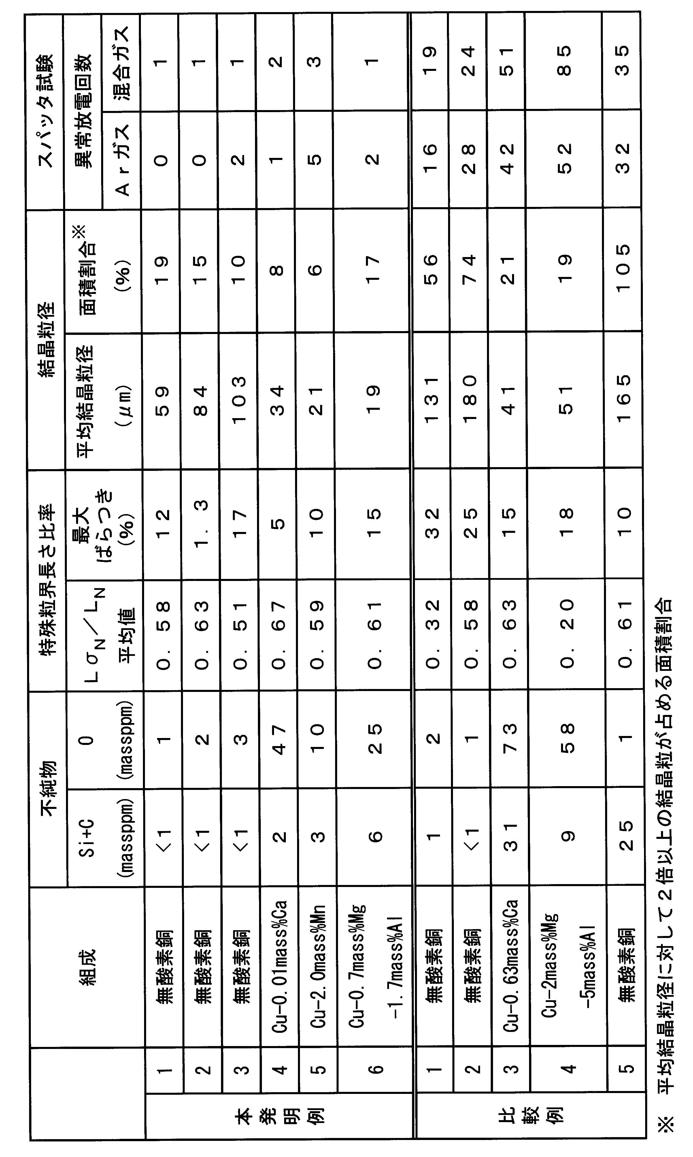
これに対して、本発明例1-6では、スパッタ試験においてArガス及び混合ガスのいずれの条件でも異常放電回数が少なくなっており、安定してスパッタを実施できることが確認された。
11 外周面
Claims (3)
- 銅又は銅合金からなる円筒型スパッタリングターゲット用素材であって、
EBSD法により、測定範囲における結晶粒界の全粒界長さLを測定し、これを単位面積1mm2当たりに換算した単位全粒界長さLNと、さらに測定範囲における特殊粒界の全特殊粒界長さLσを測定し、これを単位面積1mm2当たりに換算した単位全特殊粒界長さLσNと、によって特殊粒界長さ比率LσN/LNを定義した場合に、
軸線方向の両端部の外周面と中央部の外周面で測定した前記特殊粒界長さ比率LσN/LNの平均値が0.5以上とされるとともに、軸線方向の両端部の外周面と中央部の外周面で測定された前記特殊粒界長さ比率LσN/LNのそれぞれの値が前記平均値に対して±20%の範囲内とされており、
さらに、不純物元素であるSiとCとの含有量の総計が10質量ppm以下、O含有量が50質量ppm以下、とされている円筒型スパッタリングターゲット用素材。 - 外周面の結晶組織において、平均結晶粒径が10μm以上150μm以下の範囲内とされている請求項1に記載の円筒型スパッタリングターゲット用素材。
- 外周面の結晶組織において、平均結晶粒径に対して2倍以上の結晶粒の占める面積割合が全結晶面積の20%未満とされている請求項1又は請求項2に記載の円筒型スパッタリングターゲット用素材。
Priority Applications (5)
| Application Number | Priority Date | Filing Date | Title |
|---|---|---|---|
| CN201580000747.XA CN105209658B (zh) | 2014-04-22 | 2015-02-20 | 圆筒型溅射靶用原材料 |
| KR1020167017496A KR20160137906A (ko) | 2014-04-22 | 2015-02-20 | 원통형 스퍼터링 타깃용 소재 |
| DE112015000125.5T DE112015000125B4 (de) | 2014-04-22 | 2015-02-20 | Zylindrisches Sputter-Target-Material |
| KR1020157033056A KR20150135548A (ko) | 2014-04-22 | 2015-02-20 | 원통형 스퍼터링 타깃용 소재 |
| US14/913,028 US9748079B2 (en) | 2014-04-22 | 2015-02-20 | Cylindrical sputtering target material |
Applications Claiming Priority (2)
| Application Number | Priority Date | Filing Date | Title |
|---|---|---|---|
| JP2014088186A JP5783293B1 (ja) | 2014-04-22 | 2014-04-22 | 円筒型スパッタリングターゲット用素材 |
| JP2014-088186 | 2014-04-22 |
Publications (1)
| Publication Number | Publication Date |
|---|---|
| WO2015162986A1 true WO2015162986A1 (ja) | 2015-10-29 |
Family
ID=54200739
Family Applications (1)
| Application Number | Title | Priority Date | Filing Date |
|---|---|---|---|
| PCT/JP2015/054770 Ceased WO2015162986A1 (ja) | 2014-04-22 | 2015-02-20 | 円筒型スパッタリングターゲット用素材 |
Country Status (7)
| Country | Link |
|---|---|
| US (1) | US9748079B2 (ja) |
| JP (1) | JP5783293B1 (ja) |
| KR (2) | KR20160137906A (ja) |
| CN (1) | CN105209658B (ja) |
| DE (1) | DE112015000125B4 (ja) |
| TW (1) | TWI535867B (ja) |
| WO (1) | WO2015162986A1 (ja) |
Cited By (3)
| Publication number | Priority date | Publication date | Assignee | Title |
|---|---|---|---|---|
| WO2018066410A1 (ja) * | 2016-10-07 | 2018-04-12 | 三菱マテリアル株式会社 | 円筒型スパッタリングターゲット用熱間押出素材、及び、円筒型スパッタリングターゲットの製造方法 |
| WO2019203258A1 (ja) * | 2018-04-17 | 2019-10-24 | 三菱マテリアル株式会社 | Cu-Ni合金スパッタリングターゲット |
| JP2022042859A (ja) * | 2020-09-03 | 2022-03-15 | オリエンタル コッパー シーオー.エルティーディー. | 熱間押出プロセスからのスパッタリング法による薄膜コーティング技術のための銅ターゲットの製造 |
Families Citing this family (9)
| Publication number | Priority date | Publication date | Assignee | Title |
|---|---|---|---|---|
| KR102330631B1 (ko) * | 2016-08-17 | 2021-11-23 | 미쓰비시 마테리알 가부시키가이샤 | 원통형 실리콘 타깃 |
| JP6900642B2 (ja) * | 2016-08-26 | 2021-07-07 | 三菱マテリアル株式会社 | スパッタリングターゲット用銅素材 |
| WO2018225114A1 (ja) * | 2017-06-05 | 2018-12-13 | 凸版印刷株式会社 | 半導体装置、表示装置、及びスパッタリングターゲット |
| KR20250030002A (ko) * | 2018-09-26 | 2025-03-05 | 제이엑스금속주식회사 | 스퍼터링 타깃 및 그 제조 방법 |
| WO2020066957A1 (ja) * | 2018-09-26 | 2020-04-02 | Jx金属株式会社 | スパッタリングターゲット及びその製造方法 |
| JP7309217B2 (ja) * | 2020-06-26 | 2023-07-18 | オリエンタル コッパー シーオー.エルティーディー. | スパッタリング法を使用した薄膜コーティングのための銅円筒型ターゲットを熱間押出技術から製造する方法 |
| JP7188479B2 (ja) * | 2021-03-02 | 2022-12-13 | 三菱マテリアル株式会社 | 熱延銅合金板およびスパッタリングターゲット |
| JP7188480B2 (ja) * | 2021-03-02 | 2022-12-13 | 三菱マテリアル株式会社 | 熱延銅合金板およびスパッタリングターゲット |
| CN113862619B (zh) * | 2021-09-08 | 2023-10-17 | 先导薄膜材料(广东)有限公司 | 一种锌镁靶材及其制备方法 |
Citations (4)
| Publication number | Priority date | Publication date | Assignee | Title |
|---|---|---|---|---|
| JP2005330591A (ja) * | 2005-08-01 | 2005-12-02 | Dowa Mining Co Ltd | スパッタリングターゲット |
| JP2012111994A (ja) * | 2010-11-24 | 2012-06-14 | Furukawa Electric Co Ltd:The | 円筒状ターゲット材、その製造方法、及び、そのシート被覆方法 |
| JP2013057112A (ja) * | 2011-09-09 | 2013-03-28 | Hitachi Cable Ltd | 円筒型スパッタリングターゲット材、それを用いた配線基板及び薄膜トランジスタ |
| WO2015004958A1 (ja) * | 2013-07-08 | 2015-01-15 | Jx日鉱日石金属株式会社 | スパッタリングターゲット及び、それの製造方法 |
Family Cites Families (10)
| Publication number | Priority date | Publication date | Assignee | Title |
|---|---|---|---|---|
| JP2862727B2 (ja) | 1992-05-12 | 1999-03-03 | 同和鉱業株式会社 | 金属薄膜形成用スパッタリング・ターゲット並びにその製造方法 |
| US6139701A (en) | 1997-11-26 | 2000-10-31 | Applied Materials, Inc. | Copper target for sputter deposition |
| CN1238554C (zh) | 2002-06-24 | 2006-01-25 | 株式会社钢臂功科研 | 银合金溅射靶及其制造方法 |
| KR100700885B1 (ko) | 2003-03-17 | 2007-03-29 | 닛코킨조쿠 가부시키가이샤 | 동합금 스퍼터링 타겟트 및 그 제조방법 과 반도체 소자배선 |
| EP2014787B1 (en) * | 2006-10-03 | 2017-09-06 | JX Nippon Mining & Metals Corporation | Cu-Mn ALLOY SPUTTERING TARGET |
| US20110303535A1 (en) | 2007-05-04 | 2011-12-15 | Miller Steven A | Sputtering targets and methods of forming the same |
| JP4974198B2 (ja) | 2009-09-18 | 2012-07-11 | 古河電気工業株式会社 | スパッタリングターゲットに用いられる銅材料およびその製造方法 |
| JP5376168B2 (ja) * | 2010-03-30 | 2013-12-25 | 三菱マテリアル株式会社 | 電気銅めっき用高純度銅アノード、その製造方法および電気銅めっき方法 |
| JP5723171B2 (ja) | 2011-02-04 | 2015-05-27 | 株式会社神戸製鋼所 | Al基合金スパッタリングターゲット |
| JP5303678B1 (ja) | 2012-01-06 | 2013-10-02 | 三菱マテリアル株式会社 | 電子・電気機器用銅合金、電子・電気機器用銅合金薄板、電子・電気機器用導電部品および端子 |
-
2014
- 2014-04-22 JP JP2014088186A patent/JP5783293B1/ja active Active
-
2015
- 2015-02-20 WO PCT/JP2015/054770 patent/WO2015162986A1/ja not_active Ceased
- 2015-02-20 US US14/913,028 patent/US9748079B2/en active Active
- 2015-02-20 DE DE112015000125.5T patent/DE112015000125B4/de active Active
- 2015-02-20 KR KR1020167017496A patent/KR20160137906A/ko not_active Ceased
- 2015-02-20 CN CN201580000747.XA patent/CN105209658B/zh active Active
- 2015-02-20 KR KR1020157033056A patent/KR20150135548A/ko not_active Ceased
- 2015-02-24 TW TW104105832A patent/TWI535867B/zh active
Patent Citations (4)
| Publication number | Priority date | Publication date | Assignee | Title |
|---|---|---|---|---|
| JP2005330591A (ja) * | 2005-08-01 | 2005-12-02 | Dowa Mining Co Ltd | スパッタリングターゲット |
| JP2012111994A (ja) * | 2010-11-24 | 2012-06-14 | Furukawa Electric Co Ltd:The | 円筒状ターゲット材、その製造方法、及び、そのシート被覆方法 |
| JP2013057112A (ja) * | 2011-09-09 | 2013-03-28 | Hitachi Cable Ltd | 円筒型スパッタリングターゲット材、それを用いた配線基板及び薄膜トランジスタ |
| WO2015004958A1 (ja) * | 2013-07-08 | 2015-01-15 | Jx日鉱日石金属株式会社 | スパッタリングターゲット及び、それの製造方法 |
Cited By (5)
| Publication number | Priority date | Publication date | Assignee | Title |
|---|---|---|---|---|
| WO2018066410A1 (ja) * | 2016-10-07 | 2018-04-12 | 三菱マテリアル株式会社 | 円筒型スパッタリングターゲット用熱間押出素材、及び、円筒型スパッタリングターゲットの製造方法 |
| JP2018059171A (ja) * | 2016-10-07 | 2018-04-12 | 三菱マテリアル株式会社 | 円筒型スパッタリングターゲット用熱間押出素材、及び、円筒型スパッタリングターゲットの製造方法 |
| WO2019203258A1 (ja) * | 2018-04-17 | 2019-10-24 | 三菱マテリアル株式会社 | Cu-Ni合金スパッタリングターゲット |
| JP2019183251A (ja) * | 2018-04-17 | 2019-10-24 | 三菱マテリアル株式会社 | Cu−Ni合金スパッタリングターゲット |
| JP2022042859A (ja) * | 2020-09-03 | 2022-03-15 | オリエンタル コッパー シーオー.エルティーディー. | 熱間押出プロセスからのスパッタリング法による薄膜コーティング技術のための銅ターゲットの製造 |
Also Published As
| Publication number | Publication date |
|---|---|
| US9748079B2 (en) | 2017-08-29 |
| KR20160137906A (ko) | 2016-12-01 |
| DE112015000125T5 (de) | 2016-04-21 |
| US20160203959A1 (en) | 2016-07-14 |
| KR20150135548A (ko) | 2015-12-02 |
| CN105209658B (zh) | 2017-01-18 |
| TW201542843A (zh) | 2015-11-16 |
| CN105209658A (zh) | 2015-12-30 |
| JP5783293B1 (ja) | 2015-09-24 |
| JP2015206089A (ja) | 2015-11-19 |
| TWI535867B (zh) | 2016-06-01 |
| DE112015000125B4 (de) | 2021-05-06 |
Similar Documents
| Publication | Publication Date | Title |
|---|---|---|
| JP5783293B1 (ja) | 円筒型スパッタリングターゲット用素材 | |
| CN114269957B (zh) | 纯铜板 | |
| JP6152212B1 (ja) | Cu−Ni−Si系銅合金板材 | |
| CN105473755B (zh) | 圆筒型溅射靶用原材料的制造方法 | |
| JP5752736B2 (ja) | スパッタリング用ターゲット | |
| JP4792116B2 (ja) | 純銅板の製造方法及び純銅板 | |
| TWI485272B (zh) | Pure copper plate manufacturing methods and pure copper plate | |
| KR20120125248A (ko) | 순구리판의 제조 방법 및 순구리판 | |
| WO2021177469A1 (ja) | 純銅板 | |
| JP5461467B2 (ja) | 強度、導電率及び曲げ加工性に優れたチタン銅及びその製造方法 | |
| CN108603285B (zh) | 圆筒型溅射靶用热挤压原材料及圆筒型溅射靶的制造方法 | |
| JP6027823B2 (ja) | 熱延銅板、及び、熱延銅板の形状調整方法 | |
| JP2011132557A (ja) | 純銅板の製造方法及び純銅板 | |
| JP7131376B2 (ja) | スパッタリングターゲット用銅素材 | |
| JP5793069B2 (ja) | スパッタリング用銅ターゲット材の製造方法 | |
| CN107614745B (zh) | 铝合金溅射靶材 | |
| JP6694265B2 (ja) | 電極集電体用アルミニウム合金箔および電極集電体用アルミニウム合金箔の製造方法 | |
| JP6595188B2 (ja) | スパッタリングターゲットの製造方法 |
Legal Events
| Date | Code | Title | Description |
|---|---|---|---|
| ENP | Entry into the national phase |
Ref document number: 20157033056 Country of ref document: KR Kind code of ref document: A |
|
| 121 | Ep: the epo has been informed by wipo that ep was designated in this application |
Ref document number: 15783310 Country of ref document: EP Kind code of ref document: A1 |
|
| WWE | Wipo information: entry into national phase |
Ref document number: 14913028 Country of ref document: US |
|
| WWE | Wipo information: entry into national phase |
Ref document number: 112015000125 Country of ref document: DE |
|
| 122 | Ep: pct application non-entry in european phase |
Ref document number: 15783310 Country of ref document: EP Kind code of ref document: A1 |