WO2015159540A1 - テラヘルツ波検出器 - Google Patents
テラヘルツ波検出器 Download PDFInfo
- Publication number
- WO2015159540A1 WO2015159540A1 PCT/JP2015/002076 JP2015002076W WO2015159540A1 WO 2015159540 A1 WO2015159540 A1 WO 2015159540A1 JP 2015002076 W JP2015002076 W JP 2015002076W WO 2015159540 A1 WO2015159540 A1 WO 2015159540A1
- Authority
- WO
- WIPO (PCT)
- Prior art keywords
- wave detector
- reflective film
- film
- terahertz
- substrate
- Prior art date
Links
- 239000010408 film Substances 0.000 claims abstract description 192
- 239000000758 substrate Substances 0.000 claims abstract description 53
- 238000001514 detection method Methods 0.000 claims abstract description 30
- 238000010521 absorption reaction Methods 0.000 claims abstract description 22
- 239000010409 thin film Substances 0.000 claims abstract description 16
- 238000000926 separation method Methods 0.000 claims abstract description 14
- 230000010287 polarization Effects 0.000 claims description 43
- 230000035945 sensitivity Effects 0.000 description 29
- 230000001681 protective effect Effects 0.000 description 16
- 230000000694 effects Effects 0.000 description 11
- 239000002184 metal Substances 0.000 description 7
- 238000002310 reflectometry Methods 0.000 description 7
- 238000004519 manufacturing process Methods 0.000 description 6
- 238000010586 diagram Methods 0.000 description 5
- 238000000034 method Methods 0.000 description 4
- 238000011835 investigation Methods 0.000 description 2
- 239000010410 layer Substances 0.000 description 2
- 230000015572 biosynthetic process Effects 0.000 description 1
- 239000011229 interlayer Substances 0.000 description 1
- 230000003287 optical effect Effects 0.000 description 1
- 239000004065 semiconductor Substances 0.000 description 1
- 239000000126 substance Substances 0.000 description 1
Images


Classifications
-
- G—PHYSICS
- G01—MEASURING; TESTING
- G01J—MEASUREMENT OF INTENSITY, VELOCITY, SPECTRAL CONTENT, POLARISATION, PHASE OR PULSE CHARACTERISTICS OF INFRARED, VISIBLE OR ULTRAVIOLET LIGHT; COLORIMETRY; RADIATION PYROMETRY
- G01J5/00—Radiation pyrometry, e.g. infrared or optical thermometry
- G01J5/10—Radiation pyrometry, e.g. infrared or optical thermometry using electric radiation detectors
-
- G—PHYSICS
- G01—MEASURING; TESTING
- G01J—MEASUREMENT OF INTENSITY, VELOCITY, SPECTRAL CONTENT, POLARISATION, PHASE OR PULSE CHARACTERISTICS OF INFRARED, VISIBLE OR ULTRAVIOLET LIGHT; COLORIMETRY; RADIATION PYROMETRY
- G01J5/00—Radiation pyrometry, e.g. infrared or optical thermometry
- G01J5/02—Constructional details
- G01J5/0225—Shape of the cavity itself or of elements contained in or suspended over the cavity
- G01J5/024—Special manufacturing steps or sacrificial layers or layer structures
-
- G—PHYSICS
- G01—MEASURING; TESTING
- G01J—MEASUREMENT OF INTENSITY, VELOCITY, SPECTRAL CONTENT, POLARISATION, PHASE OR PULSE CHARACTERISTICS OF INFRARED, VISIBLE OR ULTRAVIOLET LIGHT; COLORIMETRY; RADIATION PYROMETRY
- G01J5/00—Radiation pyrometry, e.g. infrared or optical thermometry
- G01J5/02—Constructional details
- G01J5/08—Optical arrangements
- G01J5/0803—Arrangements for time-dependent attenuation of radiation signals
-
- G—PHYSICS
- G01—MEASURING; TESTING
- G01J—MEASUREMENT OF INTENSITY, VELOCITY, SPECTRAL CONTENT, POLARISATION, PHASE OR PULSE CHARACTERISTICS OF INFRARED, VISIBLE OR ULTRAVIOLET LIGHT; COLORIMETRY; RADIATION PYROMETRY
- G01J5/00—Radiation pyrometry, e.g. infrared or optical thermometry
- G01J5/02—Constructional details
- G01J5/08—Optical arrangements
- G01J5/0808—Convex mirrors
-
- G—PHYSICS
- G01—MEASURING; TESTING
- G01J—MEASUREMENT OF INTENSITY, VELOCITY, SPECTRAL CONTENT, POLARISATION, PHASE OR PULSE CHARACTERISTICS OF INFRARED, VISIBLE OR ULTRAVIOLET LIGHT; COLORIMETRY; RADIATION PYROMETRY
- G01J5/00—Radiation pyrometry, e.g. infrared or optical thermometry
- G01J5/10—Radiation pyrometry, e.g. infrared or optical thermometry using electric radiation detectors
- G01J5/20—Radiation pyrometry, e.g. infrared or optical thermometry using electric radiation detectors using resistors, thermistors or semiconductors sensitive to radiation, e.g. photoconductive devices
-
- G—PHYSICS
- G01—MEASURING; TESTING
- G01J—MEASUREMENT OF INTENSITY, VELOCITY, SPECTRAL CONTENT, POLARISATION, PHASE OR PULSE CHARACTERISTICS OF INFRARED, VISIBLE OR ULTRAVIOLET LIGHT; COLORIMETRY; RADIATION PYROMETRY
- G01J5/00—Radiation pyrometry, e.g. infrared or optical thermometry
- G01J5/10—Radiation pyrometry, e.g. infrared or optical thermometry using electric radiation detectors
- G01J2005/103—Absorbing heated plate or film and temperature detector
Definitions
- the present invention relates to a detector that detects electromagnetic waves (terahertz waves) in the terahertz frequency band, and more particularly to a bolometer-type terahertz wave detector.
- THz waves electromagnetic waves in a terahertz (THz) frequency band between light and radio waves
- electromagnetic waves having a frequency of 10 12 Hz and a wavelength of about 30 ⁇ m to 1 mm that is, electromagnetic waves having a frequency of 10 12 Hz and a wavelength of about 30 ⁇ m to 1 mm, hereinafter referred to as THz waves
- THz waves electromagnetic waves having a frequency of 10 12 Hz and a wavelength of about 30 ⁇ m to 1 mm
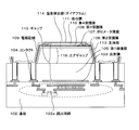
- FIG. 14 is an explanatory diagram schematically showing a pixel structure of the two-dimensional bolometer type THz wave detector described in Patent Document 3.
- FIG. 14 is a cross-sectional view of a two-dimensional bolometer type THz wave detector.
- FIG. 16 and FIG. 17 are explanatory diagrams schematically showing the pixel structure of the two-dimensional bolometer type THz wave detector described in Patent Document 4.
- FIG. 16 and FIG. 17 are explanatory diagrams schematically showing the pixel structure of the two-dimensional bolometer type THz wave detector described in Patent Document 4.
- FIG. 17 is explanatory diagrams schematically showing the pixel structure of the two-dimensional bolometer type THz wave detector described in Patent Document 4.
- the THz wave detector it is desirable to be able to detect THz waves with higher sensitivity.
- the THz wave detector described in Patent Document 3 realizes highly sensitive THz wave detection using interference between the reflection film 103 and the absorption film 111 as shown in FIG.
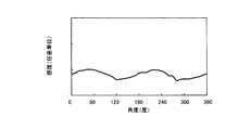
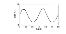
- FIG. 18 is a graph showing the polarization angle dependence of the sensor sensitivity of the THz wave detector shown in FIG. 14.
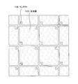
- FIG. 19 is a top view of the reflective film 103 of the arranged pixels (THz wave detector shown in FIG. 14).
- FIG. 19 shows a top view of the reflective films 103 of a plurality of pixels arranged in an overhead view.
- the THz wave passes through the gap between the reflective films 103 between the pixels, and the THz wave is reflected and absorbed by the substrate 102 (specifically, the metal wiring of the readout circuit 102a of the substrate 102). Therefore, in order to examine the THz reflection characteristics of the THz wave detector, it is necessary to estimate reflection / absorption in the metal wiring of the readout circuit 102a.
- FIG. 20 shows the THz reflection characteristics of a THz wave detector in which the structure above the reflective film 103 is not formed.
- FIG. 20 is a graph showing the reflectance polarization angle dependency of the THz wave detector shown in FIG. 14 when the structure above the reflective film 103 is not formed.
- the THz reflectivity varies greatly depending on the polarization angle. Assuming that the gap shape of the reflective film 103 is reflected in the THz reflection characteristics, in that case, the THz reflection characteristics are expected to be four-fold symmetrical repeated every 90 degrees. However, since the THz reflection characteristics shown in FIG. 20 are two-fold symmetric, it can be assumed that reflection / absorption from the metal wiring of the readout circuit 102a below the reflection film 103 occurs. That is, reflection / absorption in the metal wiring of the readout circuit 102a can be estimated from the graph shown in FIG.
- an object of the present invention is to provide a bolometer-type terahertz wave detector that can reduce the dependence of the sensor sensitivity on the polarization angle and that is more sensitive.
- the terahertz wave detector according to the present invention is supported by the support unit including the electrode wiring connected to the readout circuit formed on the substrate in a state where the temperature detection unit including the bolometer thin film connected to the electrode wiring is floated from the substrate.
- a terahertz wave detector having a thermal separation structure comprising: a reflective film that reflects a terahertz wave formed on a substrate; and an absorption film that absorbs a terahertz wave formed on a temperature detector; It is formed integrally with a reflection film of adjacent terahertz wave detectors.
- the terahertz wave detector according to the present invention is supported by the support unit including the electrode wiring connected to the readout circuit formed on the substrate in a state where the temperature detection unit including the bolometer thin film connected to the electrode wiring is floated from the substrate.
- a terahertz wave detector having a thermal separation structure, a second reflective film formed on the substrate to reflect the terahertz wave and covering the reflective film, and a temperature detector And a second reflection film formed integrally with a second reflection film of an adjacent terahertz wave detector.
- the terahertz wave detector according to the present invention is supported by the support unit including the electrode wiring connected to the readout circuit formed on the substrate in a state where the temperature detection unit including the bolometer thin film connected to the electrode wiring is floated from the substrate.
- a terahertz wave detector having a thermal separation structure comprising: a reflective film that reflects a terahertz wave formed on a substrate; and an absorption film that absorbs a terahertz wave formed on a temperature detector; It is characterized in that it is formed without a gap between the reflection films of adjacent terahertz wave detectors.
- the terahertz wave detector according to the present invention is supported by the support unit including the electrode wiring connected to the readout circuit formed on the substrate in a state where the temperature detection unit including the bolometer thin film connected to the electrode wiring is floated from the substrate.
- a terahertz wave detector having a thermal separation structure comprising: a reflective film that reflects a terahertz wave formed on a substrate; and an absorption film that absorbs a terahertz wave formed on a temperature detector; The polarization angle dependency is smaller than a predetermined value.
- the polarization angle dependency of the sensor sensitivity of the bolometer type THz wave detector can be reduced, and more sensitive THz wave detection can be realized.
- FIG. It is explanatory drawing which shows typically the pixel structure of the two-dimensional bolometer type
- FIG. It is explanatory drawing which shows typically the pixel structure of the two-dimensional bolometer type
- FIG. It is explanatory drawing which shows typically the pixel structure of the two-dimensional bolometer type
- FIG. It is explanatory drawing which shows typically the pixel structure of the two-dimensional bolometer type
- FIG. It is a graph which shows the polarization angle dependence of the sensor sensitivity of the THz wave detector shown in FIG.
- Embodiment 1 FIG. A first embodiment of the present invention will be described below with reference to the drawings.
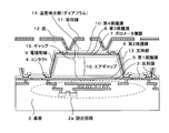
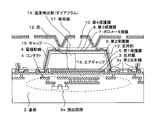
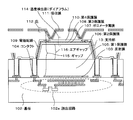
- FIG. 1 is an explanatory diagram schematically showing a pixel structure of a first embodiment of a THz wave detector according to the present invention.
- FIG. 1 shows a cross-sectional view of a THz wave detector.
- the THz wave detector includes a readout circuit 2a, a substrate 2, a reflective film 3, a contact 4, a first protective film 5, an electrode wiring 9, a flange 12, and a support portion 13. And a temperature detection unit (diaphragm) 14.
- the substrate 2, the readout circuit 2a, the reflection film 3, the contact 4, the first protective film 5, the electrode wiring 9, the flange 12, the support portion 13 and the temperature detection portion 14 are the substrate 102, the readout circuit 102a, Since it is the same as the reflective film 103, the contact 104, the first protective film 105, the electrode wiring 109, the collar 112, the support part 113, and the temperature detection part 114, the description thereof is omitted.
- the second protective film 6, the third protective film 8, and the fourth protective film 10 included in the support part 13 are the second protective film 106, the third protective film 108, and the second protective film included in the support part 113 illustrated in FIG. 14. Since it is the same as 4 protective film 110, description is abbreviate
- the bolometer thin film 7 and the absorption film 11 included in the temperature detection unit 14 are the same as the bolometer thin film 107 and the absorption film 111 included in the temperature detection unit 114 illustrated in FIG.
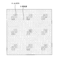
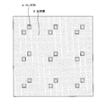
- FIG. 2 is a top view of the reflective film 3 shown in FIG.
- FIG. 2 shows a top view of the reflective films 3 of a plurality of pixels arranged in an overhead view.
- the gap between the reflective films 3 is not formed to prevent the THz wave from passing through, and reflection / absorption from the metal wiring of the readout circuit 2a is prevented. Thereby, the polarization angle dependency of the THz reflectance of the substrate 2 can be reduced.
- the reflective film is integrally formed. However, the reflective film need not be formed integrally, and the reflective film 3 may be formed as a separate body as long as no gap is left. .
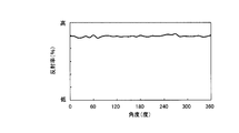
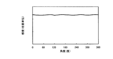
- FIG. 5 shows the polarization angle dependency of the sensor sensitivity as shown in FIG. 18, and the effect of the present invention is remarkably exhibited.
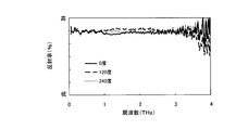
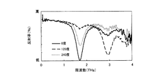
- FIG. 4 is a graph showing the reflectance frequency dependency when the structure above the reflective film 3 of the THz wave detector shown in FIG. 1 is not formed.
- FIG. 4 shows the frequency dependence of the THz reflectivity when the polarization angles are 0 degrees, 120 degrees, and 240 degrees.
- FIG. 21 is a graph showing the reflectance frequency dependence when the structure above the reflective film 3 is not formed in the THz wave detector shown in FIG.
- the THz wave detector of the present embodiment can suppress variations in the polarization angle dependence of the THz reflectivity depending on the frequency, and can keep the polarization sensitivity dependence of the sensor sensitivity small even when the frequency changes.
- the reflective film 3 is formed so that there is no gap in the reflective film 3 between the pixels. Thereby, it is possible to prevent the THz wave from passing through the gap between the reflective films 3, and to reduce the polarization angle dependency of the THz reflectance of the substrate 2. Therefore, it is difficult to generate a phenomenon in which the output (sensor sensitivity) from the THz wave detector changes depending on the polarization angle. That is, according to the present invention, it is possible to reduce the dependence of the sensor sensitivity on the polarization angle in the THz wave detector that detects the THz wave using the interference between the reflection film and the absorption film as shown in FIG. .
- the reflective film 3 may be disposed between the contact 4 and the contact of another pixel.
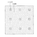
- the reflective film 3 is formed as shown in FIG.
- FIG. 6 is a top view of the entire reflection film 3 when the reflection film 3 is disposed between the contact 4 and the contact of another pixel.
- FIG. 6 shows a top view of the reflective films 3 of a plurality of pixels arranged in an overhead view.
- one of the contacts 4 of the THz wave detector may be electrically connected to the contact 4 of the other THz wave detector.
- a gap (a hole for the contact 4 formed in the reflective film 3) between the reflective film 3 and the contact 4 provided in the reflective film 3 can be reduced.
- the area of the reflective film 3 can be increased as much as possible, and the dependence of the sensor sensitivity of the THz wave detector on the polarization angle can be further reduced.
- FIG. 7 is a top view of the reflective film 3 when the contact 4 is electrically connected to contacts of other pixels.
- FIG. 7 shows a top view of the reflective films 3 of a plurality of pixels arranged in an overhead view.
- FIG. 8 is an explanatory view schematically showing a pixel structure of the second embodiment of the THz wave detector according to the present invention.
- FIG. 8 shows a cross-sectional view of the THz wave detector.
- the THz wave detector includes a second reflective film 3a in addition to the components shown in FIG.
- FIG. 9 is a top view of the second reflective film 3a shown in FIG.
- FIG. 9 shows a top view of the second reflective films 3a of a plurality of pixels arranged in an overhead view.
- the second reflective film 3 a is formed so as to cover the reflective film 3.
- the reflective film 3 and the second reflective film 3a are physically separated.
- the second reflective film 3a and the absorption film 11 form an optical resonance structure.
- This embodiment is effective when the reflective film 3 cannot be connected to the reflective film of an adjacent pixel due to the manufacture of a THz sensor. For example, when a voltage is applied to the reflective film 3, there is a possibility that a short circuit will occur if the reflective film 3 is connected to the reflective film of an adjacent pixel. In that case, by forming the second reflective film 3a physically separated from the reflective film 3 so as to cover the reflective film 3, the same effect as that of the first embodiment can be obtained.
- the effect of the present invention appears more remarkably when the sheet resistance of the second reflective film 3a is 100 ⁇ / ⁇ or less, as in the first embodiment.
- FIG. 10 is an explanatory diagram schematically showing a pixel structure of the third embodiment of the THz wave detector according to the present invention.
- FIG. 10 shows a cross-sectional view of the THz wave detector.
- the pixel structure of the third embodiment is the same as the pixel structure of the first embodiment.
- the THz wave detector does not include the trough 12.
- the distance (air gap 16) between the upper surface of the first protective film 5 and the lower surface of the temperature detection unit 14 is less than 8 ⁇ m without changing the distance (gap 15) between the reflective film 3 and the absorption film 11.
- the film thickness of the first protective film 5 is set so that
- this embodiment is an embodiment in which the reflective film 3 of the first embodiment is applied to the THz wave detector shown in FIG.
- the present invention may be applied to the THz wave detector shown in FIG.
- the same effect as the first embodiment can be obtained.
- the second reflective film 3a of the second embodiment may be applied to the THz wave detector shown in FIG. As a result, in the THz wave detector as shown in FIG. 15, even if the reflective film 3 cannot be connected to the reflective film of the adjacent pixel due to the THz sensor manufacturing, The same effect can be obtained.
- FIG. 11 is an explanatory view schematically showing a pixel structure of a fourth embodiment of the THz wave detector according to the present invention.
- FIG. 11 shows a cross-sectional view of the THz wave detector.
- the pixel structure of the fourth embodiment is the same as the pixel structure of the third embodiment. However, in the present embodiment, the ridge 12 is formed on the temperature detection unit 14.
- this embodiment is an embodiment in which the reflective film 3 of the first embodiment is applied to the THz wave detector shown in FIG.
- the present invention may be applied to the THz wave detector shown in FIG.
- an effect equivalent to that of the first embodiment can be obtained.
- the second reflective film 3a of the second embodiment may be applied to the THz wave detector shown in FIG. Thereby, in the THz wave detector as shown in FIG. 16, even if it is not possible to connect the reflective film 3 to the reflective film of the adjacent pixel due to the THz sensor manufacturing, The same effect can be obtained.
- FIG. 12 is an explanatory view schematically showing a pixel structure of the fifth embodiment of the THz wave detector according to the present invention.
- FIG. 12 shows a cross-sectional view of the THz wave detector.
- the pixel structure of the fifth embodiment is the same as the pixel structure of the second embodiment.
- vias and wiring layers are sequentially stacked on the wiring used as the reflective film 3 by using a wiring formation method in the semiconductor manufacturing process, and the electrode wiring 9 is connected to the readout circuit 2a.
- a multilayer wiring structure is formed. Thereby, disconnection of the electrode wiring 9 can be suppressed.
- the interlayer insulating film 21 is an insulating film between the stacked wiring layers.
- the present embodiment is an embodiment in which the second reflective film 3a of the second embodiment is applied to the THz wave detector shown in FIG.
- the present invention may be applied to the THz wave detector shown in FIG.
- the THz wave detector as shown in FIG. 17 even when the reflective film 3 cannot be connected to the reflective film of the adjacent pixel due to the THz sensor manufacturing, The same effect can be obtained.
- the THz wave detector shown in FIG. 17 may include the reflective film 3 instead of the reflective film 103. Even in such a form, an effect equivalent to that of the first embodiment can be obtained.
- FIG. 13 is an explanatory diagram showing the minimum configuration of the terahertz wave detector according to the present invention.
- the temperature detection unit 14 including the bolometer thin film 7 connected to the electrode wiring 9 is formed on the substrate by the support unit 13 including the electrode wiring 9 connected to the readout circuit 2 a formed on the substrate 2.
- 2 is a terahertz wave detector having a thermal separation structure supported in a floating state from 2, and includes a reflection film 3 that reflects the terahertz wave formed on the substrate 2 and a terahertz wave that is formed on the temperature detection unit 14.
- the reflective film 3 is formed integrally with the reflective film of the adjacent terahertz wave detector.
- the sheet resistance of the reflective film 3 may be 100 ⁇ / ⁇ or less. According to such a configuration, the polarization angle dependency of the sensor sensitivity of the THz wave detector can be further reduced.
- a hole for the contact 4 may be formed in the reflective film 3 in accordance with the area of the contact 4 that electrically connects the readout circuit 2 a formed on the substrate 2 and the electrode wiring 9 included in the support portion 13. . According to such a configuration, the area of the reflective film 3 can be increased as much as possible, and the polarization angle dependency of the sensor sensitivity of the THz wave detector can be further reduced.
- the terahertz wave detector includes a temperature detection unit 14 including a bolometer thin film 7 connected to the electrode wiring 9 by a support unit 13 including the electrode wiring 9 connected to the readout circuit 2 a formed on the substrate 2.
- a terahertz wave detector having a thermal separation structure supported in a floating state from the substrate 2 so as to cover the reflective film 3 on the upper side of the reflective film 3 that reflects the terahertz wave formed on the substrate 2.
- the second reflection film 3a to be formed and the absorption film 11 for absorbing the terahertz wave formed in the temperature detection unit 14 are provided, and the second reflection film 3a is integrated with the second reflection film of the adjacent terahertz wave detector. It is formed.
- the THz sensor instead of forming the reflective film 3 integrally with the reflective film of the adjacent pixel, if the second reflective film 3a covering the reflective film 3 is formed integrally with the second reflective film of the adjacent pixel, the THz sensor Even when the reflective film 3 cannot be connected to the reflective film of an adjacent pixel due to manufacturing reasons, the dependence of the sensor sensitivity on the polarization angle in the THz wave detector can be reduced.
- the reflective film 3 and the second reflective film 3a may be separated. According to such a configuration, for example, when a voltage is applied to the reflective film 3, there is a possibility of short-circuiting if the reflective film 3 is connected to the reflective film of an adjacent pixel. In that case, by physically separating the reflective film 3 and the second reflective film 3a, the dependence of the sensor sensitivity on the polarization angle in the THz wave detector can be reduced.
- the sheet resistance of the second reflective film 3a may be 100 ⁇ / ⁇ or less. According to such a configuration, the polarization angle dependency of the sensor sensitivity of the THz wave detector can be further reduced.
- the terahertz wave detector includes a temperature detection unit 14 including a bolometer thin film 7 connected to the electrode wiring 9 by a support unit 13 including the electrode wiring 9 connected to the readout circuit 2 a formed on the substrate 2.
- a terahertz wave detector having a thermal separation structure supported in a floating state from the substrate 2, the reflective film 3 reflecting the terahertz wave formed on the substrate 2, and the terahertz formed on the temperature detector 14.
- the reflection film 3 is formed without a gap from the reflection film of the adjacent terahertz wave detector.
- the THz wave passes through the gap of the reflective film 3. This can be prevented. Thereby, the polarization angle dependency of the THz reflectance of the substrate 2 can be reduced.
- the terahertz wave detector includes a temperature detection unit 14 including a bolometer thin film 7 connected to the electrode wiring 9 by a support unit 13 including the electrode wiring 9 connected to the readout circuit 2 a formed on the substrate 2.
- a terahertz wave detector having a thermal separation structure supported in a floating state from the substrate 2, the reflective film 3 reflecting the terahertz wave formed on the substrate 2, and the terahertz formed on the temperature detector 14.
- the reflection film 3 is formed so that the dependency of the terahertz wave reflectance on the polarization angle is smaller than a predetermined value.
Landscapes
- Physics & Mathematics (AREA)
- General Physics & Mathematics (AREA)
- Spectroscopy & Molecular Physics (AREA)
- Engineering & Computer Science (AREA)
- Manufacturing & Machinery (AREA)
- Photometry And Measurement Of Optical Pulse Characteristics (AREA)
Abstract
Description
以下、本発明の第1の実施形態を図面を参照して説明する。
以下、本発明の第2の実施形態を図面を参照して説明する。
以下、本発明の第3の実施形態を図面を参照して説明する。
以下、本発明の第4の実施形態を図面を参照して説明する。
以下、本発明の第5の実施形態を図面を参照して説明する。
2a、102a 読出回路
3、103 反射膜
3a 第2反射膜
4、104 コンタクト
5、105 第1保護膜
6、106 第2保護膜
7、107 ボロメータ薄膜
8、108 第3保護膜
9、109 電極配線
10、110 第4保護膜
11、111 吸収膜
12、112 庇
13、113 支持部
14、114 温度検出部(ダイアフラム)
15、115 ギャップ
16、116 エアギャップ
Claims (8)
- 基板に形成された読出回路に接続される電極配線を含む支持部により、前記電極配線に接続されるボロメータ薄膜を含む温度検出部が前記基板から浮いた状態で支持される熱分離構造を有するテラヘルツ波検出器であって、
前記基板上に形成されるテラヘルツ波を反射する反射膜と、
前記温度検出部に形成されるテラヘルツ波を吸収する吸収膜とを備え、
前記反射膜は隣り合うテラヘルツ波検出器の反射膜と一体に形成される
ことを特徴とするテラヘルツ波検出器。 - 反射膜のシート抵抗が、100Ω/□以下である
請求項1に記載のテラヘルツ波検出器。 - 基板に形成された読出回路と支持部が含む電極配線とを電気的に接続するコンタクトの面積に合わせて、反射膜に前記コンタクト用の穴が形成される
請求項1または請求項2に記載のテラヘルツ波検出器。 - 基板に形成された読出回路に接続される電極配線を含む支持部により、前記電極配線に接続されるボロメータ薄膜を含む温度検出部が前記基板から浮いた状態で支持される熱分離構造を有するテラヘルツ波検出器であって、
前記基板上に形成されるテラヘルツ波を反射する反射膜の上側に当該反射膜を覆うように形成される第2反射膜と、
前記温度検出部に形成されるテラヘルツ波を吸収する吸収膜とを備え、
前記第2反射膜は隣り合うテラヘルツ波検出器の第2反射膜と一体に形成される
ことを特徴とするテラヘルツ波検出器。 - 反射膜と第2反射膜とが分離している
請求項4に記載のテラヘルツ波検出器。 - 第2反射膜のシート抵抗が、100Ω/□以下である
請求項4または請求項5に記載のテラヘルツ波検出器。 - 基板に形成された読出回路に接続される電極配線を含む支持部により、前記電極配線に接続されるボロメータ薄膜を含む温度検出部が前記基板から浮いた状態で支持される熱分離構造を有するテラヘルツ波検出器であって、
前記基板上に形成されるテラヘルツ波を反射する反射膜と、
前記温度検出部に形成されるテラヘルツ波を吸収する吸収膜とを備え、
前記反射膜は隣り合うテラヘルツ波検出器の反射膜と隙間なく形成される
ことを特徴とするテラヘルツ波検出器。 - 基板に形成された読出回路に接続される電極配線を含む支持部により、前記電極配線に接続されるボロメータ薄膜を含む温度検出部が前記基板から浮いた状態で支持される熱分離構造を有するテラヘルツ波検出器であって、
前記基板上に形成されるテラヘルツ波を反射する反射膜と、
前記温度検出部に形成されるテラヘルツ波を吸収する吸収膜とを備え、
前記反射膜はテラヘルツ波反射率の偏光角度依存性が所定値より小さくなるように形成される
ことを特徴とするテラヘルツ波検出器。
Priority Applications (4)
| Application Number | Priority Date | Filing Date | Title |
|---|---|---|---|
| US15/302,237 US20170030775A1 (en) | 2014-04-18 | 2015-04-04 | Terahertz-wave detector |
| EP15780439.4A EP3133379A4 (en) | 2014-04-18 | 2015-04-15 | Terahertz-wave detector |
| CA2945597A CA2945597C (en) | 2014-04-18 | 2015-04-15 | Terahertz-wave detector |
| JP2016513642A JP6292297B2 (ja) | 2014-04-18 | 2015-04-15 | テラヘルツ波検出器 |
Applications Claiming Priority (2)
| Application Number | Priority Date | Filing Date | Title |
|---|---|---|---|
| JP2014086412 | 2014-04-18 | ||
| JP2014-086412 | 2014-04-18 |
Publications (1)
| Publication Number | Publication Date |
|---|---|
| WO2015159540A1 true WO2015159540A1 (ja) | 2015-10-22 |
Family
ID=54323763
Family Applications (1)
| Application Number | Title | Priority Date | Filing Date |
|---|---|---|---|
| PCT/JP2015/002076 WO2015159540A1 (ja) | 2014-04-18 | 2015-04-15 | テラヘルツ波検出器 |
Country Status (5)
| Country | Link |
|---|---|
| US (1) | US20170030775A1 (ja) |
| EP (1) | EP3133379A4 (ja) |
| JP (1) | JP6292297B2 (ja) |
| CA (1) | CA2945597C (ja) |
| WO (1) | WO2015159540A1 (ja) |
Cited By (2)
| Publication number | Priority date | Publication date | Assignee | Title |
|---|---|---|---|---|
| WO2017094280A1 (ja) * | 2015-11-30 | 2017-06-08 | 国立大学法人東京大学 | ボロメータ型テラヘルツ波検出素子およびボロメータ型テラヘルツ波検出素子アレイ |
| WO2017094769A1 (ja) * | 2015-11-30 | 2017-06-08 | 国立大学法人東京大学 | ボロメータ型テラヘルツ波検出素子アレイ |
Families Citing this family (1)
| Publication number | Priority date | Publication date | Assignee | Title |
|---|---|---|---|---|
| CN107128872B (zh) * | 2017-05-11 | 2018-09-18 | 烟台睿创微纳技术股份有限公司 | 一种新型偏振非制冷红外焦平面探测器及其制备方法 |
Citations (7)
| Publication number | Priority date | Publication date | Assignee | Title |
|---|---|---|---|---|
| JP2002071452A (ja) * | 2000-08-29 | 2002-03-08 | Nec Corp | 熱型赤外線検出器 |
| JP2005043381A (ja) * | 2004-10-18 | 2005-02-17 | Nec Corp | 熱型赤外線検出器およびその製造方法 |
| JP2009025306A (ja) * | 2007-07-20 | 2009-02-05 | Ulis | 電磁放射検出器およびこの検出器の製造方法 |
| JP2009222649A (ja) * | 2008-03-18 | 2009-10-01 | Mitsubishi Electric Corp | 赤外線撮像素子およびその製造方法 |
| JP2012002603A (ja) * | 2010-06-15 | 2012-01-05 | Nec Corp | ボロメータ型テラヘルツ波検出器 |
| JP2013164364A (ja) * | 2012-02-13 | 2013-08-22 | Seiko Epson Corp | テラヘルツカメラ及び電子機器 |
| JP2014032088A (ja) * | 2012-08-02 | 2014-02-20 | Mitsubishi Electric Corp | 電磁波センサ及び電磁波センサ装置 |
Family Cites Families (5)
| Publication number | Priority date | Publication date | Assignee | Title |
|---|---|---|---|---|
| JP3921320B2 (ja) * | 2000-01-31 | 2007-05-30 | 日本電気株式会社 | 熱型赤外線検出器およびその製造方法 |
| FR2855609B1 (fr) * | 2003-05-26 | 2005-07-01 | Commissariat Energie Atomique | Dispositif de detection bolometrique a antenne, a cavite optimisee, pour ondes electromagnetiques millimetriques ou submillimetriques, et procede de fabrication de ce dispositif |
| US8495882B2 (en) * | 2009-08-10 | 2013-07-30 | General Electric Company | Syngas cleanup section with carbon capture and hydrogen-selective membrane |
| EP2618817B1 (en) * | 2010-07-31 | 2018-06-13 | The Scripps Research Institute | Liposome targeting compounds and related uses |
| FR2977937B1 (fr) * | 2011-07-15 | 2013-08-16 | Centre Nat Rech Scient | Detecteur bolometrique a performances ameliorees |
-
2015
- 2015-04-04 US US15/302,237 patent/US20170030775A1/en not_active Abandoned
- 2015-04-15 CA CA2945597A patent/CA2945597C/en active Active
- 2015-04-15 EP EP15780439.4A patent/EP3133379A4/en not_active Withdrawn
- 2015-04-15 JP JP2016513642A patent/JP6292297B2/ja active Active
- 2015-04-15 WO PCT/JP2015/002076 patent/WO2015159540A1/ja active Application Filing
Patent Citations (7)
| Publication number | Priority date | Publication date | Assignee | Title |
|---|---|---|---|---|
| JP2002071452A (ja) * | 2000-08-29 | 2002-03-08 | Nec Corp | 熱型赤外線検出器 |
| JP2005043381A (ja) * | 2004-10-18 | 2005-02-17 | Nec Corp | 熱型赤外線検出器およびその製造方法 |
| JP2009025306A (ja) * | 2007-07-20 | 2009-02-05 | Ulis | 電磁放射検出器およびこの検出器の製造方法 |
| JP2009222649A (ja) * | 2008-03-18 | 2009-10-01 | Mitsubishi Electric Corp | 赤外線撮像素子およびその製造方法 |
| JP2012002603A (ja) * | 2010-06-15 | 2012-01-05 | Nec Corp | ボロメータ型テラヘルツ波検出器 |
| JP2013164364A (ja) * | 2012-02-13 | 2013-08-22 | Seiko Epson Corp | テラヘルツカメラ及び電子機器 |
| JP2014032088A (ja) * | 2012-08-02 | 2014-02-20 | Mitsubishi Electric Corp | 電磁波センサ及び電磁波センサ装置 |
Non-Patent Citations (1)
| Title |
|---|
| See also references of EP3133379A4 * |
Cited By (3)
| Publication number | Priority date | Publication date | Assignee | Title |
|---|---|---|---|---|
| WO2017094280A1 (ja) * | 2015-11-30 | 2017-06-08 | 国立大学法人東京大学 | ボロメータ型テラヘルツ波検出素子およびボロメータ型テラヘルツ波検出素子アレイ |
| WO2017094769A1 (ja) * | 2015-11-30 | 2017-06-08 | 国立大学法人東京大学 | ボロメータ型テラヘルツ波検出素子アレイ |
| JPWO2017094280A1 (ja) * | 2015-11-30 | 2018-09-13 | 国立大学法人 東京大学 | ボロメータ型テラヘルツ波検出素子およびボロメータ型テラヘルツ波検出素子アレイ |
Also Published As
| Publication number | Publication date |
|---|---|
| US20170030775A1 (en) | 2017-02-02 |
| EP3133379A4 (en) | 2017-11-22 |
| EP3133379A1 (en) | 2017-02-22 |
| JP6292297B2 (ja) | 2018-03-14 |
| CA2945597A1 (en) | 2015-10-22 |
| JPWO2015159540A1 (ja) | 2017-04-13 |
| CA2945597C (en) | 2019-01-15 |
Similar Documents
| Publication | Publication Date | Title |
|---|---|---|
| US8541742B2 (en) | Bolometer-type THz wave detector | |
| US9520510B2 (en) | Embedded optical sensors using transverse Fabry-Perot resonator as detectors | |
| KR101910573B1 (ko) | 광대역 광 흡수체를 포함하는 적외선 검출기 | |
| JP4964935B2 (ja) | 半導体光素子および半導体光装置 | |
| US8598528B2 (en) | Infrared detector based on suspended bolometric micro-plates | |
| US20140264029A1 (en) | Terahertz wave detection device, camera, imaging device, and measuring device | |
| US9121761B2 (en) | Infrared detectors | |
| US9638578B2 (en) | Terahertz wave detecting device, camera, imaging apparatus, and measuring apparatus | |
| JP6292297B2 (ja) | テラヘルツ波検出器 | |
| WO2010079686A1 (ja) | 光検出器 | |
| TW201629446A (zh) | 熱測量器型THz檢測器 | |
| US11215510B2 (en) | Thermal infrared detector and manufacturing method for thermal infrared detector | |
| JP6225582B2 (ja) | 熱型赤外線センサー | |
| JP2012177696A (ja) | 半導体光素子および半導体光装置 | |
| US20200249084A1 (en) | Light detector | |
| US11255730B2 (en) | Light detector | |
| EP3557203B1 (en) | Light detector | |
| JP6834974B2 (ja) | ボロメータ型テラヘルツ波検出器 | |
| US11519785B2 (en) | Light detector | |
| JP2010101675A (ja) | 赤外線撮像素子およびその製造方法 | |
| JP2015135264A (ja) | 焦電型光検出器、焦電型光検出装置、電子機器 | |
| WO2017094769A1 (ja) | ボロメータ型テラヘルツ波検出素子アレイ | |
| JP2014153187A (ja) | 半導体物理量センサ | |
| JP2010185708A (ja) | ボロメータ型赤外線センサ |
Legal Events
| Date | Code | Title | Description |
|---|---|---|---|
| 121 | Ep: the epo has been informed by wipo that ep was designated in this application |
Ref document number: 15780439 Country of ref document: EP Kind code of ref document: A1 |
|
| ENP | Entry into the national phase |
Ref document number: 2016513642 Country of ref document: JP Kind code of ref document: A |
|
| WWE | Wipo information: entry into national phase |
Ref document number: 15302237 Country of ref document: US |
|
| ENP | Entry into the national phase |
Ref document number: 2945597 Country of ref document: CA |
|
| REEP | Request for entry into the european phase |
Ref document number: 2015780439 Country of ref document: EP |
|
| WWE | Wipo information: entry into national phase |
Ref document number: 2015780439 Country of ref document: EP |
|
| NENP | Non-entry into the national phase |
Ref country code: DE |