WO2015152244A1 - センサ素子およびその製造方法ならびに検出装置およびその製造方法 - Google Patents
センサ素子およびその製造方法ならびに検出装置およびその製造方法 Download PDFInfo
- Publication number
- WO2015152244A1 WO2015152244A1 PCT/JP2015/060135 JP2015060135W WO2015152244A1 WO 2015152244 A1 WO2015152244 A1 WO 2015152244A1 JP 2015060135 W JP2015060135 W JP 2015060135W WO 2015152244 A1 WO2015152244 A1 WO 2015152244A1
- Authority
- WO
- WIPO (PCT)
- Prior art keywords
- sensor element
- main surface
- forming
- protective film
- manufacturing
- Prior art date
- Legal status (The legal status is an assumption and is not a legal conclusion. Google has not performed a legal analysis and makes no representation as to the accuracy of the status listed.)
- Ceased
Links
Images










Classifications
-
- G—PHYSICS
- G01—MEASURING; TESTING
- G01F—MEASURING VOLUME, VOLUME FLOW, MASS FLOW OR LIQUID LEVEL; METERING BY VOLUME
- G01F1/00—Measuring the volume flow or mass flow of fluid or fluent solid material wherein the fluid passes through a meter in a continuous flow
- G01F1/68—Measuring the volume flow or mass flow of fluid or fluent solid material wherein the fluid passes through a meter in a continuous flow by using thermal effects
- G01F1/684—Structural arrangements; Mounting of elements, e.g. in relation to fluid flow
- G01F1/688—Structural arrangements; Mounting of elements, e.g. in relation to fluid flow using a particular type of heating, cooling or sensing element
- G01F1/69—Structural arrangements; Mounting of elements, e.g. in relation to fluid flow using a particular type of heating, cooling or sensing element of resistive type
- G01F1/692—Thin-film arrangements
-
- B—PERFORMING OPERATIONS; TRANSPORTING
- B81—MICROSTRUCTURAL TECHNOLOGY
- B81C—PROCESSES OR APPARATUS SPECIALLY ADAPTED FOR THE MANUFACTURE OR TREATMENT OF MICROSTRUCTURAL DEVICES OR SYSTEMS
- B81C1/00—Manufacture or treatment of devices or systems in or on a substrate
- B81C1/00642—Manufacture or treatment of devices or systems in or on a substrate for improving the physical properties of a device
- B81C1/0065—Mechanical properties
- B81C1/00674—Treatments for improving wear resistance
-
- B—PERFORMING OPERATIONS; TRANSPORTING
- B81—MICROSTRUCTURAL TECHNOLOGY
- B81B—MICROSTRUCTURAL DEVICES OR SYSTEMS, e.g. MICROMECHANICAL DEVICES
- B81B3/00—Devices comprising flexible or deformable elements, e.g. comprising elastic tongues or membranes
- B81B3/0064—Constitution or structural means for improving or controlling the physical properties of a device
- B81B3/0067—Mechanical properties
- B81B3/0075—For improving wear resistance
-
- B—PERFORMING OPERATIONS; TRANSPORTING
- B81—MICROSTRUCTURAL TECHNOLOGY
- B81C—PROCESSES OR APPARATUS SPECIALLY ADAPTED FOR THE MANUFACTURE OR TREATMENT OF MICROSTRUCTURAL DEVICES OR SYSTEMS
- B81C1/00—Manufacture or treatment of devices or systems in or on a substrate
- B81C1/00642—Manufacture or treatment of devices or systems in or on a substrate for improving the physical properties of a device
- B81C1/0065—Mechanical properties
- B81C1/00666—Treatments for controlling internal stress or strain in MEMS structures
-
- B—PERFORMING OPERATIONS; TRANSPORTING
- B81—MICROSTRUCTURAL TECHNOLOGY
- B81B—MICROSTRUCTURAL DEVICES OR SYSTEMS, e.g. MICROMECHANICAL DEVICES
- B81B2201/00—Specific applications of microelectromechanical systems
- B81B2201/02—Sensors
- B81B2201/0264—Pressure sensors
-
- B—PERFORMING OPERATIONS; TRANSPORTING
- B81—MICROSTRUCTURAL TECHNOLOGY
- B81B—MICROSTRUCTURAL DEVICES OR SYSTEMS, e.g. MICROMECHANICAL DEVICES
- B81B2203/00—Basic microelectromechanical structures
- B81B2203/03—Static structures
- B81B2203/0315—Cavities
-
- B—PERFORMING OPERATIONS; TRANSPORTING
- B81—MICROSTRUCTURAL TECHNOLOGY
- B81B—MICROSTRUCTURAL DEVICES OR SYSTEMS, e.g. MICROMECHANICAL DEVICES
- B81B2207/00—Microstructural systems or auxiliary parts thereof
- B81B2207/99—Microstructural systems or auxiliary parts thereof not provided for in B81B2207/01 - B81B2207/115
-
- B—PERFORMING OPERATIONS; TRANSPORTING
- B81—MICROSTRUCTURAL TECHNOLOGY
- B81C—PROCESSES OR APPARATUS SPECIALLY ADAPTED FOR THE MANUFACTURE OR TREATMENT OF MICROSTRUCTURAL DEVICES OR SYSTEMS
- B81C2201/00—Manufacture or treatment of microstructural devices or systems
- B81C2201/01—Manufacture or treatment of microstructural devices or systems in or on a substrate
- B81C2201/0101—Shaping material; Structuring the bulk substrate or layers on the substrate; Film patterning
- B81C2201/0102—Surface micromachining
-
- B—PERFORMING OPERATIONS; TRANSPORTING
- B81—MICROSTRUCTURAL TECHNOLOGY
- B81C—PROCESSES OR APPARATUS SPECIALLY ADAPTED FOR THE MANUFACTURE OR TREATMENT OF MICROSTRUCTURAL DEVICES OR SYSTEMS
- B81C2201/00—Manufacture or treatment of microstructural devices or systems
- B81C2201/01—Manufacture or treatment of microstructural devices or systems in or on a substrate
- B81C2201/0101—Shaping material; Structuring the bulk substrate or layers on the substrate; Film patterning
- B81C2201/0111—Bulk micromachining
-
- B—PERFORMING OPERATIONS; TRANSPORTING
- B81—MICROSTRUCTURAL TECHNOLOGY
- B81C—PROCESSES OR APPARATUS SPECIALLY ADAPTED FOR THE MANUFACTURE OR TREATMENT OF MICROSTRUCTURAL DEVICES OR SYSTEMS
- B81C2201/00—Manufacture or treatment of microstructural devices or systems
- B81C2201/01—Manufacture or treatment of microstructural devices or systems in or on a substrate
- B81C2201/0101—Shaping material; Structuring the bulk substrate or layers on the substrate; Film patterning
- B81C2201/0128—Processes for removing material
- B81C2201/0143—Focussed beam, i.e. laser, ion or e-beam
-
- B—PERFORMING OPERATIONS; TRANSPORTING
- B81—MICROSTRUCTURAL TECHNOLOGY
- B81C—PROCESSES OR APPARATUS SPECIALLY ADAPTED FOR THE MANUFACTURE OR TREATMENT OF MICROSTRUCTURAL DEVICES OR SYSTEMS
- B81C2201/00—Manufacture or treatment of microstructural devices or systems
- B81C2201/01—Manufacture or treatment of microstructural devices or systems in or on a substrate
- B81C2201/0161—Controlling physical properties of the material
-
- B—PERFORMING OPERATIONS; TRANSPORTING
- B81—MICROSTRUCTURAL TECHNOLOGY
- B81C—PROCESSES OR APPARATUS SPECIALLY ADAPTED FOR THE MANUFACTURE OR TREATMENT OF MICROSTRUCTURAL DEVICES OR SYSTEMS
- B81C2201/00—Manufacture or treatment of microstructural devices or systems
- B81C2201/05—Temporary protection of devices or parts of the devices during manufacturing
- B81C2201/053—Depositing a protective layers
-
- G—PHYSICS
- G01—MEASURING; TESTING
- G01F—MEASURING VOLUME, VOLUME FLOW, MASS FLOW OR LIQUID LEVEL; METERING BY VOLUME
- G01F1/00—Measuring the volume flow or mass flow of fluid or fluent solid material wherein the fluid passes through a meter in a continuous flow
- G01F1/68—Measuring the volume flow or mass flow of fluid or fluent solid material wherein the fluid passes through a meter in a continuous flow by using thermal effects
- G01F1/684—Structural arrangements; Mounting of elements, e.g. in relation to fluid flow
- G01F1/6845—Micromachined devices
Definitions
- the present invention relates to a sensor element used in a semiconductor or MEMS (Micro Electro Mechanical System, hereinafter referred to as MEMS) technology, and more particularly to a sensor element in which a cavity structure is formed by anisotropic etching from the back surface of a substrate.
- MEMS Micro Electro Mechanical System
- Recent sensor elements tend to have a more delicate and complex structure by adopting microfabrication and techniques applying semiconductor and MEMS technologies.
- examples of sensor elements having a cavity (thin film hollow structure) formed by partially removing the substrate include a pressure sensor, an ultrasonic sensor, and a flow rate sensor.
- a temperature-dependent resistor is formed at the top of the cavity structure. That is, the detection part of the flow sensor is formed on the cavity structure. Specifically, a heating element and an intake air temperature detecting body are formed on the upper part of the cavity structure, and the element is controlled so that the temperature of the heating element is higher than the temperature detected by the intake air temperature detecting body. Using the structure, a voltage corresponding to the amount of heat radiated from the heating element to the fluid is output.
- a method of forming a cavity structure in such a sensor element for example, there is a method of performing a wet etching process using a mask film having an opening on a region where the cavity structure is formed in a semiconductor substrate.
- Japanese Patent Laid-Open No. 11-295127 describes a side flow rate detecting element in which a base material protective film is formed on the back side surface and the front side surface of a base material.
- a base material protective film is formed on the back side surface and the front side surface of a base material.
- Japanese Patent Application Laid-Open No. 2013-160706 discloses KOH (potassium hydroxide), TMAH (tetramethylammonium hydroxide: the following) in a state where a backside protective film is formed in addition to a thermal oxide film on the backside of a silicon wafer.
- TMAH tetramethylammonium hydroxide
- JP 2012-98072 A describes a flow rate detection device in which textured irregularities are formed on a surface facing a built-in portion where a sensor element is arranged. It is described that by forming irregularities, it is possible to improve the contact of the adhesive that bonds the sensor element and the support and to suppress the seepage of the underflow preventive agent.
- JP 2013-518425 A describes a method of manufacturing a photovoltaic cell including a step of performing an isotropic etching process after an anisotropic etching process is performed on a crystalline silicon substrate.
- a linear scratch or an indentation may occur in the protective film due to foreign matters such as silicon dust.
- the etchant enters from the scratches or indentations, resulting in rectangular etching marks (pits), or abnormal etching of the base material, resulting in a cavity portion that is larger than the design dimension. May spread and cause variations in the shape of the cavity.
- pits rectangular etching marks
- the reliability of the sensor element may be reduced by being pressurized in the use state.
- the textured irregularities described in Japanese Patent Application Laid-Open No. 2012-98072 and Japanese Translation of PCT International Application No. 2013-518425 are based on the etching rate difference between the (100) plane and the (111) plane of silicon. It is formed by deposition of a slow (111) plane. Such irregularities have a problem that the convex portions are sharp and are easily chipped, and pits are easily generated.
- the unevenness of the texture structure has a portion where the (111) plane is exposed. Therefore, a semiconductor substrate having such irregularities is easily broken along the (111) plane when pressed with foreign matter or the like in the irregularities, and includes a semiconductor substrate having such irregularities formed.
- the sensor element has a problem that pressure resistance is not sufficient.
- a main object of the present invention is to provide a sensor element, a manufacturing method thereof, a detection apparatus, and a manufacturing method thereof, which can suppress the formation of pits or variations in the shape of a cavity and have high resistance during pressurization. .
- the sensor element according to the present invention has a first main surface and a second main surface located on the opposite side of the first main surface, and a cavity structure is formed on the second main surface side.
- the tip of the convex part of the part has a curved shape.
- the method for manufacturing a sensor element according to the present invention includes a step of preparing a semiconductor substrate having a first main surface and a second main surface located on the opposite side of the first main surface, and a second semiconductor substrate. Forming a concavo-convex shape portion on the main surface, forming a protective film on the concavo-convex shape portion, forming an opening pattern in the protective film, and exposing it in the opening pattern using the protective film as a mask A step of forming a cavity structure by etching a semiconductor substrate, and a step of forming a detection element on the first main surface side in a region where the cavity structure is formed, The concavo-convex shape portion is formed such that the tip of the convex portion of the concavo-convex shape portion has a curved shape.
- a sensor element a manufacturing method thereof, a detection device, and a manufacturing method thereof, which can suppress the formation of pits or variations in the shape of the cavity and have high resistance during pressurization.
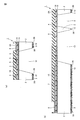
- FIG. 4 is a top view for explaining the sensor element according to Embodiment 1.
- FIG. FIG. 2 is a cross-sectional view taken along line II-II in FIG.
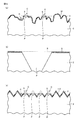
- FIG. 3 is a cross-sectional view for explaining a concavo-convex shape portion of the sensor element according to Embodiment 1.
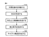
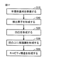
- 3 is a flowchart of a method for manufacturing the sensor element according to the first embodiment.
- FIG. 6 is a cross-sectional view for explaining the method for manufacturing the sensor element according to the first embodiment.
- FIG. 6 is a cross-sectional view for explaining the method for manufacturing the sensor element according to the first embodiment.
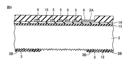
- FIG. 6 is a cross-sectional view for explaining the method for manufacturing the sensor element according to the first embodiment.
- FIG. 6 is a cross-sectional view for explaining the method for manufacturing the sensor element according to the first embodiment.
- FIG. 6 is a cross-sectional view for explaining the method for manufacturing the sensor element according to the first embodiment.
- FIG. 6 is a cross-sectional view for explaining the method for manufacturing the sensor element according to the first embodiment.
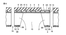
- FIG. 6 is a cross-sectional view for explaining the method for manufacturing the sensor element according to the first embodiment. It is the top view seen from arrow XI in FIG.
- FIG. 6 is a cross-sectional view for explaining the method for manufacturing the sensor element according to the first embodiment.
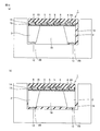
- FIG. 6 is a cross-sectional view for explaining the operational effect of the sensor element according to the first embodiment.
- FIG. 6 is a cross-sectional view for explaining the operational effect of the sensor element according to the first embodiment.
- FIG. 6 is a top view for explaining a detection device according to a second embodiment.
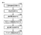
- FIG. 16 is a cross-sectional view taken along the line XVI-XVI in FIG. 6 is a flowchart of a modification of the method for manufacturing the sensor element according to the first embodiment. It is a fragmentary sectional view of the 2nd main surface of the semiconductor substrate after the process of forming the uneven
- 6 is a flowchart of a sensor element manufacturing method according to Embodiment 3.
- 10 is a flowchart of a modification of the method for manufacturing the sensor element according to the third embodiment.
- the sensor element 1 according to Embodiment 1 is a flow rate detection element used in a flow rate detection device, for example.
- the sensor element 1 includes a semiconductor substrate 2 having a first main surface 2A and a second main surface 2B located on the opposite side of the first main surface 2A.
- the first main surface 2A is a surface that faces a fluid path that is a detection target of the sensor element 1, and is a surface that contacts the fluid.
- cavity structures 9 and 10 are formed on the second main surface 2B side.
- the cavity structures 9 and 10 are provided so as to reach the first main surface 2A from the second main surface 2B and the semiconductor substrate 2 has a so-called reverse taper shape.
- the first main surface 2A is formed over a wider area than the second main surface 2B.
- the thickness of the semiconductor substrate 2 may be an arbitrary size, for example, 0.5 mm.
- the material which comprises the semiconductor base material 2 can be made into arbitrary semiconductor materials, it is silicon (Si), for example.
- the 2nd main surface 2B of the semiconductor substrate 2 On the second main surface 2B of the semiconductor substrate 2, an uneven portion 12 is formed over the entire surface, and a lower protective film 3 is formed on the entire region of the uneven portion 12.
- the 2nd main surface 2B has predetermined surface roughness by the uneven
- the concavo-convex portion 12 and the lower protective film 3 are formed so that the ten-point average roughness Rz (old JIS2001) of the second main surface 2B is larger than the film thickness of the lower protective film 3.
- the ten-point average roughness Rz of the first main surface 2A is smaller than that of the second main surface, and the first main surface 2A is, for example, a mirror surface.
- the ten-point average roughness Rz of the second main surface 2B of the semiconductor substrate 2 is 0.05 ⁇ m or more, preferably 1.00 ⁇ m or more. Further, the arithmetic average roughness Ra of the second main surface 2B is, for example, 0.01 ⁇ m or more, and preferably 0.25 ⁇ m or more. From the viewpoint of suppressing the formation of etch pits, the ten-point average roughness Rz of the second main surface 2B is preferably large. In general, if the roughness Rz is excessively increased, the strength of the semiconductor substrate 2 is reduced, and there is a concern about the occurrence of cracks or the like. It is good also as an upper limit of Rz.
- the upper limit value of the roughness Rz may be set to 5.00 ⁇ m. If the roughness Rz is limited within such a numerical range, etch pit formation can be sufficiently suppressed while suppressing a decrease in the strength of the semiconductor substrate 2.
- the convex part tip of the uneven part 12 is rounded. If it says from a different viewpoint, the shape of the uneven
- the concavo-convex shape portion 12 is not a quadrangular pyramid formed so that a plurality of surfaces formed so as to extend radially from the apex in the semiconductor substrate 2 intersect with each other, for example.
- the convex end portion of the concavo-convex shape portion 12 is formed in, for example, a hemispherical shape.
- the thickness of the lower protective film 3 is, for example, not less than 0.25 ⁇ m and not more than 1.50 ⁇ m, and preferably not less than 0.50 ⁇ m and not more than 1.00 ⁇ m.
- the material constituting the lower protective film 3 is, for example, silicon dioxide (SiO 2 ).
- the lower protective film 3 can be formed by thermal oxidation using, for example, Si as a material constituting the semiconductor substrate 2.
- the lower protective film 3 does not have to be formed on the concavo-convex shape portion 12 so as to have a uniform film thickness. As long as the ten-point average roughness Rz of the second main surface 2B and the film thickness of the lower protective film 3 satisfy the above relational expression, the film thickness of the lower protective film 3 may vary.
- an upper protective film 13 and a support film 14 are formed so as to cover the openings of the cavity structures 9 and 10 from the first main surface 2A.
- the material constituting the upper protective film 13 can be any material having electrical insulation, but is, for example, SiO 2 .
- the upper protective film 13 can be formed simultaneously with the lower protective film 3, for example.
- the material constituting the support film 14 can be any material that has electrical insulation and can support the detection elements 4 and 5, and is, for example, silicon nitride (SiN), SiO 2, or the like.
- detection elements 4 and 5 are formed on the first main surface 2A side of the region where the cavity structures 9 and 10 are formed.
- the detection element 4 is, for example, an intake air temperature detection body 4, and the detection element 5 is, for example, a heating element 5.
- the intake air temperature detector 4 is on the upper protective film 13 formed in the region where the cavity structure 9 is formed, and the heating element 5 is on the upper protective film 13 formed in the region where the cavity structure 10 is formed. Each is formed.
- the intake air temperature detection body 4 and the heating element 5 are electrically connected to the electrode pad 8 via the wiring patterns 6 and 7, respectively.
- a plurality of electrode pads 8 are formed, and are electrically connected via the wiring pattern 7 to the electrode pad 8, which is electrically connected to the intake air temperature detector 4 via the wiring pattern 6.
- the electrode pads 8 are electrically insulated from each other.
- the wiring patterns 6 and 7 and the electrode pad 8 are formed on the support film 14.
- the intake air temperature detector 4 and the heating element 5 are formed to meander on the support film 14. As a result, the contact area between the intake air temperature detector 4 and the heating element 5 and the fluid to be detected can be widened.
- the positional relationship between the intake air temperature detection body 4 and the heating element 5 can be an arbitrary positional relationship.
- the sensor element 1 is configured as a flow rate detection device
- the flow direction A (See FIG. 15).
- the intake air temperature detector 4 and the heating element 5 may be arranged in series with respect to the fluid flow direction A.
- the plane dimension (hereinafter simply referred to as plane dimension) on the first main surface 2A of the intake air temperature detector 4 is arbitrary as long as the contact area between the intake air temperature detector 4 and the fluid to be detected is sufficiently obtained.
- the dimension parallel to the direction A in which the fluid to be detected flows is 0.3 mm or more and 0.8 mm or less, and the dimension intersecting the direction A is 0.2 mm or more and 0. .6 mm or less.
- the planar dimension of the heating element 5 can be any dimension as long as a sufficient amount of heat can be applied to the fluid to be detected.
- the plane dimension is parallel to the direction A in which the fluid to be detected flows.
- the dimension in the direction crossing the direction A is 0.8 mm or more and 1.8 mm or less.
- the planar dimension of the intake air temperature detection body 4 is provided to be smaller than the planar dimension of the heating element 5, for example.
- the planar dimension of the intake air temperature detection body 4 is provided to be smaller than the planar dimension of the heating element 5, for example.
- the dimension of the cavity structure 9 is formed so as to be larger than the planar dimension on the first main surface 2A of the intake air temperature detection body 4, and for example, parallel to the direction A in which the fluid to be detected flows and the direction A Is larger than the intake air temperature detector 4 by 0.7 mm or more in each of the directions intersecting with.
- the dimension of the cavity structure 10 is formed so as to be larger than the planar dimension of the first main surface 2A of the heating element 5, and for example, parallel to the direction A in which the fluid to be detected flows and in the direction A
- Each of the intersecting directions is larger than the heating element 5 by 0.7 mm or more.
- the intake air temperature detection body 4 and the heating element 5 may be formed as arbitrary structures using arbitrary constituent materials, respectively.
- each of them is a thermal resistor made of a metal thin film such as platinum (Pt). May be formed as a resistance temperature detector).
- the film thickness of the intake air temperature detector 4 and the heating element 5 is, for example, not less than 100 nm and not more than 500 nm.
- a surface protective film 15 is formed on the upper protective film 13 and the support film 14 so as to cover the intake air temperature detection body 4, the heating element 5, and the wiring patterns 6 and 7.
- the material constituting the surface protective film 15 can be any material having electrical insulation, but can be, for example, SiN or SiO 2 .
- the method for manufacturing the sensor element 1 includes a step of preparing a semiconductor substrate 2 having a first main surface 2A and a second main surface 2B located on the opposite side of the first main surface 2A (S10); A step (S20) of forming the uneven portion 12 on the second main surface 2B of the semiconductor substrate 2, a step (S30) of forming a protective film (lower protective film 3) on the uneven portion 12, and a cavity structure In the region where 9, 10 is formed, a step (S40) of forming the detection elements 4 and 5 on the first main surface 2A side, an opening pattern is formed in the protective film (lower protective film 3), and the lower protective film A step (S50) of forming the cavity structures 9 and 10 by etching the semiconductor substrate 2 exposed in the opening pattern using 3 as a mask.
- a semiconductor substrate 2 having a first main surface 2A and a second main surface 2B located on the opposite side of the first main surface 2A is prepared (step (S10)).
- the semiconductor substrate 2 can be prepared as a substrate made of any semiconductor material in which at least the first main surface 2A is mirror-polished.
- the first main surface 2A and the second main surface 2B are mirror-polished.
- a silicon substrate may be used.
- the semiconductor substrate 2 has a wafer thickness of 625 ⁇ m, for example.
- corrugated shaped part 12 is formed in the 2nd main surface 2B of the semiconductor base material 2 (process (S20)).
- the convex end of the concavo-convex portion 12 is rounded, and the ten-point average roughness Rz of the second main surface 2B is later. Any method can be adopted as long as it can be formed to be larger than the film thickness of the lower protective film 3 formed in the step (S30).
- the concavo-convex shape portion 12 can be formed by grinding and roughening the second main surface 2B.
- the ten-point average roughness Rz of the concavo-convex shape portion 12 can be set to 0.06 ⁇ m or more and 5.0 ⁇ m or less.
- the lower protective film 3 is formed on the uneven portion 12 (step (S30)). Specifically, referring to FIG. 7, lower protective film 3 is formed on the entire surface of second main surface 2B.
- a method for forming the lower protective film 3 any film forming method such as sputtering or CVD (chemical vapor deposition) can be adopted.
- CVD chemical vapor deposition
- the lower protective film 3 can be formed as a thermal oxide film (SiO 2 ). Specifically, for example, heat treatment is performed at a treatment temperature of 800 ° C. or higher and 1100 ° C.
- the thermal oxide film formed on the first main surface 2 ⁇ / b> A corresponds to the upper protective film 13
- the thermal oxide film formed on the second main surface 2 ⁇ / b> B corresponds to the lower protective film 3. That is, the upper protective film 13 and the lower protective film 3 can be formed simultaneously by subjecting the semiconductor substrate 2 to a thermal oxidation treatment.
- the detection elements 4 and 5 are formed on the first main surface 2A side (step (S40)). Specifically, on the upper protective film 13 formed on the first main surface 2A, the support film 14, the intake air temperature detecting body 4, the heating element 5, the wiring patterns 6 and 7, the electrode pad 8 and the surface protection. A film 15 is formed.
- the support film 14 As a method for forming the support film 14, for example, a reactive sputtering method or a CVD method can be employed.
- the film formation conditions for reactive sputtering can be arbitrarily selected according to the configuration of the support film 14.
- the support film 14 made of SiN is obtained by performing sputtering in a nitrogen gas atmosphere using Si as a target material. Can be formed. In this case, the deposition rate can be increased compared to the case where SiN is used as the target material.
- the support film 14 When the film is formed by the CVD method, the support film 14 can be formed by setting the film forming temperature to 300 ° C. or higher and 400 ° C. or lower using atmospheric pressure CVD, low pressure CVD, plasma CVD, or the like.
- the support film 14 is made of a nitride film such as SiN, for example, ammonia gas is used as a source gas, for example, in addition to monosilane, disilane and the like.
- an oxide film of the support film 14 such as SiO 2 is the raw material gas as example monosilane, other such disilane, etc. nitrous oxide or oxygen gas is used.
- a method for providing the support film 14 made of SiO 2 a TEOS-CVD method can be employed. Since the CVD method has better step coverage and better stress control than the sputtering method, a dense and thin film can be formed by using the CVD method for forming the support film 14 and the surface protective film 15. .
- the intake air temperature detector 4, the heating element 5, the wiring patterns 6 and 7, and the electrode pad 8 can be formed by any method.
- the film is formed by vapor deposition or sputtering, and is patterned by dry etching or wet etching using a mask pattern formed by photolithography. In this way, a predetermined current path pattern is formed in the sensor element 1.
- an opening pattern is formed in the region where the cavity structures 9 and 10 are to be formed in the lower protective film 3.
- the region where the cavity structure 9 is to be formed is a region where the intake air temperature detector 4 is to be formed, and the region where the cavity structure 10 is to be formed is a region where the heating element 5 is to be formed.
- An arbitrary method can be adopted as a method of forming the opening pattern in the lower protective film 3, but for example, a photolithography method or a dry etching method can be adopted.
- a mask pattern (not shown) having an opening pattern is formed on the lower protective film 3 in a region where the cavity structures 9 and 10 are to be formed by photolithography, and the lower protection is performed using the mask pattern.
- the lower protective film 3 having an opening pattern may be formed in a region where the cavity structures 9 and 10 are to be formed by dry etching the film 3.
- cavity structures 9 and 10 are formed by partially etching the semiconductor substrate 2 from the second main surface 2B side using the lower protective film 3 as a mask (steps). (S50)). Since the lower protective film 3 formed in the previous step (S40) has an opening pattern in a region where the cavity structures 9 and 10 are to be formed, the semiconductor substrate 2 is etched using this as a mask, whereby the cavity structure 9 , 10 can be formed in the respective regions where the cavity structures 9, 10 are to be formed.
- Arbitrary methods can be adopted as the method of forming the cavity structures 9 and 10, for example, a wet etching method using TMAH, KOH, or the like.
- the cavity structures 9 and 10 extending from the second main surface 2B to the first main surface 2A can be formed by immersing the semiconductor substrate 2 in a bathtub heated with TMAH, KOH, or the like. it can.
- An upper protective film 13 is exposed inside the cavity structures 9 and 10, and an intake air temperature detector 4 and a heating element 5 are formed on the upper protective film 13.
- the cavity structures 9 and 10 are closed by the upper protective film 13 on the first main surface 2A side. In this way, a plurality of sensor elements 1 are formed on the semiconductor substrate 2.
- the plurality of sensor elements 1 formed on the semiconductor substrate 2 are separated.
- An arbitrary method can be adopted as a method of dividing the sensor element 1 into pieces.
- a blade dicing method can be used.
- the dicing line 16 is provided in a region where the cavity structures 9 and 10 are not formed.
- the sensor element 1 according to Embodiment 1 can be obtained.
- the 2nd main surface 2B of the semiconductor base material 2 in the sensor element 1 contains the uneven
- the second main surface 2B located on the opposite side of the detection elements 4 and 5 in the sensor element 1 often comes into contact with the stages of various manufacturing apparatuses in the manufacturing process of the sensor element 1.
- the foreign matter F (see FIG. 3) having a size larger than the film thickness of the protective film is present on the stage and the second.
- a scratch S on the line may be formed in the lower protective film 3 (see FIG. 14A).
- the scratch S on the line formed in the lower protective film 3 by the step (S50) in this way becomes an etchant intrusion path in the step (S50), it is large in the region where the scratch S is formed in the lower protective film 3.
- a pit P is formed.
- the scratch S is formed on the region adjacent to the region where the cavity structures 9 and 10 are to be formed, the dimensions of the cavity structures 9 and 10 are more than the design dimensions. And the shape of the cavity structures 9 and 10 is different from the design shape 21 thereof. For example, referring to FIG. 14A, when a scratch S is formed in a region adjacent to the region 17 where the cavity structure 9 is to be formed, the distance between the scratch S and the region 17 is the longest.
- the cavity structure 9 can be formed to extend to a position.
- the scratch S is adjacent to the other side intersecting with the one side and in a direction along the direction in which the one side extends.
- the length of the one side of the cavity structure 9 becomes L2 by extending the distance L2-L1 from L1.
- the conventional sensor element in which the concavo-convex shape portion 12 is not formed becomes vulnerable to pressurization, and the conventional sensor element may be damaged due to local stress concentration when it is assembled to a support. there were.
- the sensor element 1 according to the first embodiment has the concavo-convex shape portion 12 formed on the second main surface 2B, and therefore, compared with the conventional sensor element in which the concavo-convex shape portion 12 is not formed.
- the scratch S can be finely divided.
- the pit P formed by the etchant entering from each scratch S can be reduced in size, and even if the scratch S is formed adjacent to the region where the cavity structures 9 and 10 are to be formed. Further, it is possible to greatly reduce the disorder of the shape of the cavity structures 9 and 10. As a result, even when the sensor element 1 is pressurized, the stress concentration is relaxed and is not easily damaged.
- the conventional sensor element formed as a cone shape having the concave and convex portion as shown in FIG. 13C has a finer scratch S than the conventional sensor element shown in FIG.
- the tip of the protruding portion of the uneven shape portion is likely to be chipped, In some cases, the tip of the protruding portion lacking in this way may cause a scratch S on the lower protective film 3 as a new foreign material.
- the sensor element 1 according to the first embodiment can suppress chipping of the convex portion tip because the convex portion tip of the concavo-convex shape portion 12 is formed in a curved surface, and the lower protective film 3. Can be sufficiently reduced. As a result, the deformation of the cavity structures 9 and 10 of the sensor element 1 can be sufficiently suppressed, and the stress concentration is relaxed even during pressurization, so that damage is unlikely to occur.
- the ten-point average roughness Rz of the concavo-convex shape portion 12 is equal to or greater than the film thickness of the lower protective film 3.
- the uneven portion 12 is not completely flattened by the lower protective film 3, and the lower surface 3B of the lower protective film 3 has the uneven shape of the second main surface 2B on which the uneven portion 12 is formed. It has a concavo-convex shape inherited to some extent.
- the size corresponding to the sum of the film thickness of the lower protective film 3 and the ten-point average roughness Rz of the concavo-convex shape portion 12 between the second main surface 2B and the stages of various manufacturing apparatuses is about Even when foreign matter F having an outer diameter R (see FIG. 3) is present, the lower surface 3B and the second main surface 2B are formed with irregularities due to the ten-point average roughness Rz. Further, it is possible to prevent the scratches S penetrating the lower protective film 3 from extending in a linear manner due to the relative movement of the foreign matter F and the sensor element 1 or the like. As a result, in the sensor element 1, it is suppressed that the scratch S applied to the lower protective film 3 by the foreign matter F is formed in a wide range as in the conventional sensor element.
- the convex portion tip of the concavo-convex shape portion 12 has a curved shape.
- the concavo-convex shape portion 12 is formed so as to have. For this reason, as described above, since it is possible to prevent the scratches S extending linearly from entering the lower protective film 3, it is possible to greatly reduce the disorder of the shape of the cavity structures 9 and 10. As a result, even when the obtained sensor element 1 is pressurized, the stress concentration is relaxed and is not easily damaged.
- the concavo-convex portion 12 and the lower protective film 3 are such that the ten-point average roughness of the concavo-convex portion 12 is the film of the protective film. It is formed so as to be more than the thickness. For this reason, as described above, when the sensor element 1 is fixed to the support and the flow rate detection device is assembled, the contact area between the sensor element 1 and the adhesive that connects and fixes the sensor element 1 and the support is widened. In addition, since an anchor effect can be exerted on the adhesive, the adhesion between the sensor element 1 and the support can be enhanced.
- the concavo-convex shape portion 12 is formed by grinding, for example, by changing the particle size of the abrasive grains of the grinding stone according to the size of the scratch to be suppressed, the sensor element The deformation of one cavity structure 9, 10 can be effectively suppressed.
- the ten-point average roughness Rz of the concavo-convex shape portion 12 can be increased by using a grinding wheel having a large particle size, and the ten-point average roughness Rz formed on the concavo-convex shape portion 12 can be increased. It is possible to suppress the distance that the scratch S extends on the lower protective film 3 having a thin film thickness.
- the desired concavo-convex shape portion 12 can be formed only by rough polishing (lapping) on the second main surface 2B of the semiconductor substrate 2, texture structuring and mirror surface processing steps can be reduced. Furthermore, the amount of abrasive (abrasive grains) used can be reduced, and the amount of abrasive grains used with a high environmental load can be suppressed. As a result, according to the method for manufacturing the sensor element 1 according to the first embodiment, the manufacturing cost can be reduced as compared with the conventional method for manufacturing the sensor element.
- the process (S40) of forming the detection elements 4 and 5 is performed after the process (S20) of forming the concavo-convex part 12, the tip of the convex part of the concavo-convex part 12 is curved in the process (S20).
- the process of forming the support film 14 is performed. It can be shortened.
- the concavo-convex shape portion 12 is formed by grinding (rough polishing) the second main surface 2B by using a grinding wheel having a large particle size.
- the concavo-convex shape portion 12 may be formed, for example, by grinding the roughened second main surface 2B using a grinding wheel having a smaller particle size after the rough polishing.
- the variation in the thickness of the semiconductor substrate 2 can be reduced as compared with the case where the uneven portion 12 is formed only by rough polishing.
- the bending strength of the semiconductor substrate 2 itself is lowered.
- the bending of the semiconductor substrate 2 itself is performed. Strength can be increased.
- the uneven portion 12 is formed by grinding the second main surface 2B, but is not limited thereto.
- the uneven portion 12 may be formed by ion milling.
- the uneven portion 12 may be formed by sputtering the entire surface of the second main surface 2B of the semiconductor substrate 2 using, for example, argon (Ar) plasma. Even if it does in this way, there can exist an effect similar to the manufacturing method of the sensor element 1 which concerns on Embodiment 1 mentioned above.
- corrugated shaped part 12 can be formed, without using an abrasive
- the uneven portion 12 may be formed by sandblasting, for example. Even if it does in this way, the uneven
- the concavo-convex portion 12 is formed over the entire surface of the second main surface 2B, but is not limited thereto.
- the uneven portion 12 may be formed only on the second main surface 2B located on the region where the semiconductor substrate 2 other than the region where the cavity structures 9 and 10 are to be formed, for example. Even if it does in this way, there can exist an effect similar to the manufacturing method of the sensor element which concerns on Embodiment 1. FIG.
- the lower protective film 3 is formed on the concavo-convex portion 12, and the lower protective film 3 is removed after the step of forming the cavity structures 9 and 10 (S50). Also good. Specifically, the lower protective film 3 may be removed by wet etching by immersing the second main surface 2B side of the semiconductor substrate 2 in buffered hydrofluoric acid (BHF) or the like. As a result, it is possible to form the sensor element 1 that has the cavity structures 9 and 10 and the concavo-convex shape portion 12 is exposed.
- BHF buffered hydrofluoric acid
- the detection apparatus 100 is the sensor element 1 according to the first embodiment, and the sensor element 1 from which the lower protective film 3 is removed and the concavo-convex shape portion 12 is exposed is fixed to the support 20.
- the support 20 has a built-in part in which the sensor element 1 is arranged and assembled, and the built-in part is provided so as to accommodate the sensor element 1.
- the support 20 is installed on a pipeline through which the fluid to be measured flows.
- the sensor element 1 is fixed in the built-in part of the support 20.
- the sensor element 1 and the support 20 are fixed by, for example, bonding the concave and convex portion 12 located below the region where the electrode pad 8 is formed and the support 20 with an adhesive 18.
- a region where the sensor element 1 and the support 20 are opposed to each other and located on the upstream side in the flow direction A of the fluid to be measured with respect to the cavity structures 9 and 10 is filled with a bottom flow preventing agent 19.
- the material constituting the adhesive 18 can be any adhesive that can bond the sensor element 1 and the support 20, but is preferably a thermosetting adhesive.
- the material constituting the bottom flow preventive agent 19 can be any material that can be filled between the sensor element 1 and the support 20, and is, for example, a room temperature curing adhesive.
- the manufacturing method of the detection device 100 according to the second embodiment includes a step of preparing the sensor element 1 by the sensor element manufacturing method according to the first embodiment (S100) and a support provided so that the sensor element 1 can be attached.
- the sensor element 1 according to the first embodiment is prepared by the sensor element manufacturing method according to the first embodiment described above. Furthermore, the lower protective film 3 of the obtained sensor element 1 is removed, and the sensor element 1 in which the uneven portion 12 is exposed is prepared. Subsequently, in the step of preparing the support 20 (S110), the above-described support 20 may be prepared by an arbitrary method.
- the adhesive 18 and the underflow preventive agent 19 are applied in advance to predetermined regions in the built-in portion of the support 20, respectively.
- the adhesive 18 is applied to a region located below the electrode pad 8 when the sensor element 1 is fixed, and the underflow preventive agent 19 is fixed to the sensor element 1 in the built-in portion of the support 20.
- To the cavity structures 9 and 10 are applied to a region located upstream in the flow direction A of the fluid to be measured.
- the application amount of the underflow preventive agent 19 is not pressed by the sensor element 1 when the sensor element 1 is assembled in the incorporating portion of the support 20 and protrudes to the first main surface 2A side of the sensor element 1.
- the second main surface 2B is adjusted so as not to protrude into the cavity structures 9 and 10.
- the sensor element 1 is assembled in the assembling part of the support 20.
- the sensor element 1 is pressed against the support 20.
- the adhesive 18 and the underflow preventive agent 19 applied in advance in the built-in portion of the support 20 are pressed by the uneven shape portion 12 of the sensor element 1 and are positioned between the sensor element 1 and the support 20. Expanded into the area.
- the underflow preventive agent 19 moves through the gap formed between the sensor element 1 and the support 20 and is filled to the same height as the first main surface 2A of the sensor element 1.
- the detection apparatus 100 according to Embodiment 2 can be obtained.
- the detection device 100 uses the sensor element 1 according to Embodiment 1 as a flow rate detection element. Since the cavity structures 9 and 10 of the sensor element 1 are accurately formed with respect to the design dimensions, the sensor element 1 is added to the support 20 in the step of bonding the sensor element 1 and the support 20 (S120). The sensor element 1 is not damaged even if pressed. As a result, the detection apparatus 100 can have a high yield.
- the concave-convex shape portion 12 is formed on the second main surface 2B, when the sensor element 1 is incorporated in the assembling portion of the support body 20, the second main surface 2B is interposed between the second main surface 2B and the support body 20. A void having a predetermined volume is formed. For this reason, since the adhesive 18 and the bottom flow preventive agent 19 enter the gap, the contact area between the second main surface 2B and the adhesive 18 and the bottom flow preventive agent 19 is increased. And the support 20 can be improved. Moreover, it can suppress that the adhesive agent 18 and the underflow preventive agent 19 protrude on the 1st main surface 2A and the cavity structures 9 and 10. FIG.
- the lower protective film 3 formed on the concavo-convex shape portion 12 is removed in the method for manufacturing the sensor element 1 according to the first embodiment, but the present invention is not limited to this. Absent.
- the support 20 may be bonded in a state where the lower protective film 3 is formed. Even if it does in this way, there can exist an effect similar to the detection apparatus 100 which concerns on Embodiment 2. FIG.
- the sensor element 1 according to the first embodiment is formed as a flow rate detection element
- the detection device 100 according to the second embodiment is formed as a flow rate detection device, but is not limited thereto.
- the sensor element 1 can be any sensor element having the cavity structures 9 and 10, and may be, for example, a pressure sensor or an ultrasonic sensor.
- the detection device 100 can be any detection device including a sensor element having the cavity structures 9 and 10, and may be, for example, a pressure detection device or an ultrasonic detection device.
- the step (S40) of forming the detection elements 4 and 5 is performed after the step (S20) of forming the concavo-convex shape portion 12, but is not limited thereto. It is not a thing. Referring to FIG. 17, the step (S40) of forming detection elements 4 and 5 may be performed before the step (S20) of forming uneven portion 12. Specifically, first, similarly to the method for manufacturing the sensor element according to the first embodiment, after performing the step (S10) of preparing the semiconductor substrate 2, the first main surface of the prepared semiconductor substrate 2 The step (S40) of forming the detection elements 4 and 5 on 2A may be performed.
- Cavity structures 9 and 10 are formed by forming an opening pattern in the protective film (lower protective film 3) and etching the semiconductor substrate 2 exposed in the opening pattern using the lower protective film 3 as a mask.
- Step (S50) may be performed. Even in this way, the sensor element 1 according to Embodiment 1 can be manufactured. Furthermore, since the thickness of the semiconductor substrate 2 is thick and difficult to crack in the step (S40), the defect occurrence rate due to cracking or the like can be reduced. Further, the scratch formed on the second main surface 2B in the step (S40) can be removed during the grinding in the step (S20).
- the sensor element 1 according to Embodiment 3 will be described.
- the uneven portion 12 is formed by a method such as grinding in the step (S20) of forming the uneven portion 12 of the manufacturing method of the sensor element 1 according to Embodiment 1, the second main surface of the sensor element 1 In 2B, a crushed layer 30 as shown in FIG. 18 may be formed.
- the thickness of the semiconductor substrate 2 is more than 100 ⁇ m, it is unlikely that insufficient strength in the semiconductor substrate 2 will be a serious problem even if the crushed layer 30 is formed.
- the thickness of the semiconductor substrate 2 is as small as 100 ⁇ m or less, the strength of the semiconductor substrate 2 may be insufficient due to the formation of the crushed layer 30.
- the sensor element 1 according to the third embodiment basically includes the same configuration as that of the sensor element 1 according to the first embodiment, but differs in that the crushed layer 30 is not formed on the second main surface 10B. . Therefore, the sensor element 1 according to the third embodiment can achieve the same effects as the sensor element 1 according to the first embodiment, and has sufficient strength even when the thickness of the semiconductor substrate 2 is 100 ⁇ m or less. Have high pressure resistance.
- the manufacturing method of the sensor element 1 according to the third embodiment basically has the same configuration as the manufacturing method of the sensor element 1 according to the first embodiment shown in FIG. It differs in that it includes a step (S60) of removing the crushed layer 30 formed on the second main surface 2B in the step (S20).
- the step (S60) of removing the crushed layer 30 is performed after the step (S20) of forming the uneven portion 12 and before the step of forming the protective film (S30).
- wet etching is performed on the second main surface 2B of the semiconductor substrate 2.
- the etching solution is an aqueous solution such as TMAH or KOH.
- the second main surface 2B of the semiconductor substrate 2 is immersed in a bath in which such an etching solution is heated. If it does in this way, the crushing layer 30 currently formed in the 2nd main surface 2B can be removed.
- the manufacturing method of the sensor element according to the third embodiment the same effect as that of the manufacturing method of the sensor element 1 according to the first embodiment can be obtained, and the crushing layer 30 can be easily removed. It is possible to manufacture the sensor element 1 having high resistance at the time of pressurization.
- the manufacturing method of sensor element 1 according to the third embodiment is basically the same as the modification of the manufacturing method of sensor element 1 according to the first embodiment shown in FIG. Even if it differs from this modification by the point provided with the process and the process (S60) of removing the crushing layer 30 formed in the 2nd main surface 2B in the process (S20) of forming the uneven
- the uneven shape portion 12 is formed on the second main surface 2B of the semiconductor substrate 2 after the step (S40) of forming the detection elements 4 and 5 on the first main surface 2A of the semiconductor substrate 2.
- the method is performed after the step (S20). Then, the step (S60) of removing the crushed layer 30 is performed before the step (S30). Even if it does in this way, there can exist an effect similar to the manufacturing method of the sensor element 1 which concerns on Embodiment 3.
- FIG. 1 the manufacturing method of the sensor element 1 in which the forming step (S20) and the step (S30) of forming the protective film (the lower protective film 3) on the concavo-convex shape portion 12 are performed.
- the present invention is particularly advantageously applied to a sensor element having a cavity structure.
- SYMBOLS 1 Sensor element 2 Semiconductor substrate, 2A 1st main surface, 2B 2nd main surface, 3 Lower protective film, 3B lower surface, 4 Intake temperature detection body (detection element), 5 Heat generating body (detection element), 6 , 7 Wiring pattern, 8 Electrode pad, 9, 10 Cavity structure, 12 Concavity and convexity part, 13 Upper protective film, 14 Support film, 15 Surface protective film, 16 Dicing line, 18 Adhesive, 19 Underflow preventive, 20 Support , 100 detection device.
Landscapes
- Engineering & Computer Science (AREA)
- Mechanical Engineering (AREA)
- Microelectronics & Electronic Packaging (AREA)
- Manufacturing & Machinery (AREA)
- Physics & Mathematics (AREA)
- Fluid Mechanics (AREA)
- General Physics & Mathematics (AREA)
- Computer Hardware Design (AREA)
- Measuring Volume Flow (AREA)
- Micromachines (AREA)
- Mechanical Treatment Of Semiconductor (AREA)
- Pressure Sensors (AREA)
Abstract
Description
図1~図3を参照して、実施の形態1に係るセンサ素子1について説明する。実施の形態1に係るセンサ素子1は、たとえば流量検出装置に用いられる流量検出素子である。センサ素子1は、第1の主面2Aおよび第1の主面2Aと反対側に位置する第2の主面2Bとを有する半導体基材2を備える。第1の主面2Aは、センサ素子1の検出対象である流体の経路に面する面であり、流体と接触する面である。
次に、図15および図16を参照して、実施の形態2に係る検出装置100について説明する。検出装置100は、実施の形態1に係るセンサ素子1であって、下部保護膜3が除去されて凹凸形状部12が表出しているセンサ素子1が支持体20に固定されて構成されている。支持体20は、センサ素子1が配置・組込まれる組込み部を有しており、当該組み込み部はセンサ素子1を収容可能に設けられている。支持体20は、被計測流体が流通する管路上に設置されている。センサ素子1は、支持体20の組込み部内に固定されている。センサ素子1と支持体20とは、たとえば電極パッド8が形成されている領域の下方に位置する凹凸形状部12と支持体20とが接着剤18により接着されていることにより固定されている。キャビティ構造9,10に対して被計測流体の流通方向Aの上流側に位置しセンサ素子1と支持体20とが対向する領域には、底流防止剤19が充填されている。
次に、実施の形態3に係るセンサ素子1について説明する。実施の形態1に係るセンサ素子1の製造方法の凹凸形状部12を形成する工程(S20)において凹凸形状部12を研削などの方法により形成した場合には、センサ素子1の第2の主面2Bには図18に示されるような破砕層30が形成される場合がある。半導体基材2の厚みが100μm超えである場合には、破砕層30が形成されていることによっても半導体基材2において強度不足が大きな問題となる可能性は低い。しかし、半導体基材2の厚みが100μm以下と薄い場合には、破砕層30が形成されていることにより半導体基材2が強度不足となる場合がある。実施の形態3に係るセンサ素子1は、基本的には実施の形態1に係るセンサ素子1と同様の構成を備えるが、第2の主面10Bに破砕層30が形成されていない点で異なる。そのため、実施の形態3に係るセンサ素子1は、実施の形態1に係るセンサ素子1と同様の効果を奏することができるとともに、半導体基材2の厚みが100μm以下であっても十分な強度を有しており、高い加圧耐性を有している。
Claims (13)
- 第1の主面と、前記第1の主面と反対側に位置する第2の主面とを有し、前記第2の主面側にキャビティ構造が形成されている半導体基材と、
前記キャビティ構造が形成されている領域において、前記第1の主面側に形成されている検出素子とを備え、
前記半導体基材の前記第2の主面は凹凸形状部を含み、
前記凹凸形状部の凸部先端は曲面形状を有している、センサ素子。 - 前記凹凸形状部上に形成された保護膜をさらに備え、
前記凹凸形状部の十点平均粗さは前記保護膜の膜厚以上である、請求項1に記載のセンサ素子。 - 請求項1または請求項2に記載のセンサ素子を備えた、検出装置。
- 第1の主面と、前記第1の主面と反対側に位置する第2の主面とを有する半導体基板を準備する工程と、
前記半導体基板の前記第2の主面に凹凸形状部を形成する工程と、
前記凹凸形状部上に保護膜を形成する工程と、
前記保護膜に対して開口パターンを形成し、前記保護膜をマスクとして用いて前記開口パターン内に表出している前記半導体基板をエッチングすることにより、キャビティ構造を形成する工程と、
前記キャビティ構造が形成される領域において、前記第1の主面側に検出素子を形成する工程とを備え、
前記凹凸形状部を形成する工程では、前記凹凸形状部の凸部先端が曲面形状を有するように前記凹凸形状部が形成される、センサ素子の製造方法。 - 前記凹凸形状部を形成する工程と前記保護膜を形成する工程とにおいて、前記凹凸形状部と前記保護膜とは、前記凹凸形状部の十点平均粗さが前記保護膜の膜厚以上となるように形成される、請求項4に記載のセンサ素子の製造方法。
- 前記凹凸形状部を形成する工程では、研削により前記凹凸形状部が形成される、請求項4または請求項5に記載のセンサ素子の製造方法。
- 前記凹凸形状部を形成する工程では、イオンミリングにより前記凹凸形状部が形成される、請求項4または請求項5に記載のセンサ素子の製造方法。
- 前記凹凸形状部を形成する工程では、サンドブラストにより前記凹凸形状部が形成される、請求項4または請求項5に記載のセンサ素子の製造方法。
- 前記保護膜を形成する工程では、前記第2の主面を熱酸化することにより前記保護膜が形成される、請求項4~請求項8のいずれか1項に記載のセンサ素子の製造方法。
- 前記検出素子を形成する工程は、前記凹凸形状部を形成する工程の前に実施される、請求項4~請求項9のいずれか1項に記載のセンサ素子の製造方法。
- 前記検出素子を形成する工程は、前記凹凸形状部を形成する工程の後に実施される、請求項4~請求項9のいずれか1項に記載のセンサ素子の製造方法。
- 前記凹凸形状部を形成する工程において前記第2の主面には破砕層が形成され、
前記破砕層を除去する工程を備える、請求項4~請求項11のいずれか1項に記載のセンサ素子の製造方法。 - 請求項4~請求項12のいずれか1項に記載のセンサ素子の製造方法により前記センサ素子を準備する工程と、
前記センサ素子を取り付け可能に設けられている支持体を準備する工程と、
前記凹凸形状部を接着面として前記センサ素子と前記支持体とを接着する工程とを備える、検出装置の製造方法。
Priority Applications (3)
| Application Number | Priority Date | Filing Date | Title |
|---|---|---|---|
| US15/118,686 US20170044010A1 (en) | 2014-04-02 | 2015-03-31 | Sensor element, method for manufacturing sensor element, detection device, and method for manufacturing detection device |
| JP2016511932A JP6151437B2 (ja) | 2014-04-02 | 2015-03-31 | センサ素子およびその製造方法ならびに検出装置およびその製造方法 |
| DE112015001629.5T DE112015001629T5 (de) | 2014-04-02 | 2015-03-31 | Sensorelement, Verfahren zum Herstellen eines Sensorelements, Detektionseinrichtung sowie Verfahren zum Herstellen einer Detektionseinrichtung |
Applications Claiming Priority (2)
| Application Number | Priority Date | Filing Date | Title |
|---|---|---|---|
| JP2014-076039 | 2014-04-02 | ||
| JP2014076039 | 2014-04-02 |
Publications (1)
| Publication Number | Publication Date |
|---|---|
| WO2015152244A1 true WO2015152244A1 (ja) | 2015-10-08 |
Family
ID=54240564
Family Applications (1)
| Application Number | Title | Priority Date | Filing Date |
|---|---|---|---|
| PCT/JP2015/060135 Ceased WO2015152244A1 (ja) | 2014-04-02 | 2015-03-31 | センサ素子およびその製造方法ならびに検出装置およびその製造方法 |
Country Status (4)
| Country | Link |
|---|---|
| US (1) | US20170044010A1 (ja) |
| JP (1) | JP6151437B2 (ja) |
| DE (1) | DE112015001629T5 (ja) |
| WO (1) | WO2015152244A1 (ja) |
Cited By (1)
| Publication number | Priority date | Publication date | Assignee | Title |
|---|---|---|---|---|
| EP3599414A1 (en) | 2018-07-23 | 2020-01-29 | Shin-Etsu Chemical Co., Ltd. | Synthetic quartz glass cavity member, synthetic quartz glass cavity lid, optical device package, and making methods |
Families Citing this family (2)
| Publication number | Priority date | Publication date | Assignee | Title |
|---|---|---|---|---|
| EP3687786B1 (en) | 2017-09-28 | 2025-04-23 | BVW Invest AG | Device for dynamic fluid pinning |
| CN110868681B (zh) * | 2019-11-29 | 2021-09-14 | 绍兴中芯集成电路制造股份有限公司 | Mems麦克风翘曲补偿方法和mems麦克风晶圆 |
Citations (2)
| Publication number | Priority date | Publication date | Assignee | Title |
|---|---|---|---|---|
| JP2012098072A (ja) * | 2010-10-29 | 2012-05-24 | Mitsubishi Electric Corp | 流量検出装置 |
| JP2013160706A (ja) * | 2012-02-08 | 2013-08-19 | Mitsubishi Electric Corp | 流量検出装置、並びに、流量検出装置の製造方法 |
Family Cites Families (9)
| Publication number | Priority date | Publication date | Assignee | Title |
|---|---|---|---|---|
| JPH03268316A (ja) * | 1990-03-16 | 1991-11-29 | Fujitsu Ltd | 半導体装置の製造方法 |
| JPH11295127A (ja) * | 1998-04-06 | 1999-10-29 | Mitsubishi Electric Corp | 流量検出素子及び流量センサ並びに流量検出素子の製造方法 |
| JP4590791B2 (ja) * | 2001-07-03 | 2010-12-01 | 株式会社デンソー | センサの製造方法 |
| JP4943636B2 (ja) * | 2004-03-25 | 2012-05-30 | エルピーダメモリ株式会社 | 半導体装置及びその製造方法 |
| JP4457800B2 (ja) * | 2004-07-30 | 2010-04-28 | 株式会社デンソー | フローセンサおよびその製造方法 |
| JP2007109838A (ja) * | 2005-10-13 | 2007-04-26 | Disco Abrasive Syst Ltd | デバイスおよびその製造方法 |
| JP4918140B2 (ja) * | 2007-09-25 | 2012-04-18 | アルプス電気株式会社 | 半導体圧力センサ |
| DE102008006831A1 (de) * | 2008-01-30 | 2009-08-13 | Eads Deutschland Gmbh | Heißfilmsensor |
| FR2955707B1 (fr) * | 2010-01-27 | 2012-03-23 | Commissariat Energie Atomique | Procede de realisation d'une cellule photovoltaique avec preparation de surface d'un substrat en silicium cristallin |
-
2015
- 2015-03-31 US US15/118,686 patent/US20170044010A1/en not_active Abandoned
- 2015-03-31 JP JP2016511932A patent/JP6151437B2/ja not_active Expired - Fee Related
- 2015-03-31 DE DE112015001629.5T patent/DE112015001629T5/de not_active Withdrawn
- 2015-03-31 WO PCT/JP2015/060135 patent/WO2015152244A1/ja not_active Ceased
Patent Citations (2)
| Publication number | Priority date | Publication date | Assignee | Title |
|---|---|---|---|---|
| JP2012098072A (ja) * | 2010-10-29 | 2012-05-24 | Mitsubishi Electric Corp | 流量検出装置 |
| JP2013160706A (ja) * | 2012-02-08 | 2013-08-19 | Mitsubishi Electric Corp | 流量検出装置、並びに、流量検出装置の製造方法 |
Cited By (4)
| Publication number | Priority date | Publication date | Assignee | Title |
|---|---|---|---|---|
| EP3599414A1 (en) | 2018-07-23 | 2020-01-29 | Shin-Etsu Chemical Co., Ltd. | Synthetic quartz glass cavity member, synthetic quartz glass cavity lid, optical device package, and making methods |
| KR20200011021A (ko) | 2018-07-23 | 2020-01-31 | 신에쓰 가가꾸 고교 가부시끼가이샤 | 합성 석영 유리 캐비티, 합성 석영 유리 캐비티 리드, 광학 소자 패키지 및 이들의 제조 방법 |
| US11424389B2 (en) | 2018-07-23 | 2022-08-23 | Shin-Etsu Chemical Co., Ltd. | Synthetic quartz glass cavity member, synthetic quartz glass cavity lid, optical device package, and making methods |
| US11757067B2 (en) | 2018-07-23 | 2023-09-12 | Shin-Etsu Chemical Co., Ltd. | Synthetic quartz glass cavity member, synthetic quartz glass cavity lid, optical device package, and making methods |
Also Published As
| Publication number | Publication date |
|---|---|
| JP6151437B2 (ja) | 2017-06-21 |
| DE112015001629T5 (de) | 2017-02-09 |
| JPWO2015152244A1 (ja) | 2017-04-13 |
| US20170044010A1 (en) | 2017-02-16 |
Similar Documents
| Publication | Publication Date | Title |
|---|---|---|
| US8497149B2 (en) | MEMS device | |
| CN103969296B (zh) | 基于膜的传感器设备及其制造方法 | |
| JP6195929B2 (ja) | 電磁波を検出するための少なくとも2つのウェハを有する装置、および、当該装置の製造方法 | |
| JP2006121053A (ja) | 電子部品のための薄いガラスチップ及びその製造方法 | |
| JP2011205074A (ja) | 半導体製造装置 | |
| JP6151437B2 (ja) | センサ素子およびその製造方法ならびに検出装置およびその製造方法 | |
| CN105339297A (zh) | 用于制造包括填充有牺牲材料的腔体的半导体结构的方法 | |
| US20170355591A1 (en) | Microelectromechanical device and a method of manufacturing a microelectromechanical device | |
| WO2016093020A1 (ja) | 圧電デバイス、及び圧電デバイスの製造方法 | |
| JP5197714B2 (ja) | 流量検出装置 | |
| CN101578231B (zh) | 表面粗糙化方法 | |
| JP5692099B2 (ja) | 半導体圧力センサおよびその製造方法 | |
| TWI682630B (zh) | 複合基板及壓電元件 | |
| JP6041033B2 (ja) | 半導体基板の製造方法 | |
| WO2016008532A1 (en) | Transducer element and method of manufacturing a transducer element | |
| TW201306116A (zh) | 防止感應器上腐蝕的方法及裝置 | |
| JP2013160706A (ja) | 流量検出装置、並びに、流量検出装置の製造方法 | |
| CN102272912A (zh) | “绝缘体上半导体”型衬底的支撑衬底的测试方法 | |
| CN100510667C (zh) | 玻璃衬底和使用了该玻璃衬底的静电电容式压力传感器 | |
| JP2006047279A (ja) | ガラス基板及びそれを用いた静電容量型圧力センサ | |
| US20190237358A1 (en) | Methods of fabricating silicon-on-insulator (soi) semiconductor devices using blanket fusion bonding | |
| JP2019153902A (ja) | 複合基板の製造方法 | |
| JP2014126533A (ja) | センサ及びその製造方法 | |
| JP2017030258A (ja) | シリコン基板の加工方法 | |
| US20230377935A1 (en) | Temporary bonding method |
Legal Events
| Date | Code | Title | Description |
|---|---|---|---|
| 121 | Ep: the epo has been informed by wipo that ep was designated in this application |
Ref document number: 15773776 Country of ref document: EP Kind code of ref document: A1 |
|
| WWE | Wipo information: entry into national phase |
Ref document number: 15118686 Country of ref document: US |
|
| ENP | Entry into the national phase |
Ref document number: 2016511932 Country of ref document: JP Kind code of ref document: A |
|
| WWE | Wipo information: entry into national phase |
Ref document number: 112015001629 Country of ref document: DE |
|
| 122 | Ep: pct application non-entry in european phase |
Ref document number: 15773776 Country of ref document: EP Kind code of ref document: A1 |