WO2015147286A1 - コンデンサ用リード端子 - Google Patents
コンデンサ用リード端子 Download PDFInfo
- Publication number
- WO2015147286A1 WO2015147286A1 PCT/JP2015/059698 JP2015059698W WO2015147286A1 WO 2015147286 A1 WO2015147286 A1 WO 2015147286A1 JP 2015059698 W JP2015059698 W JP 2015059698W WO 2015147286 A1 WO2015147286 A1 WO 2015147286A1
- Authority
- WO
- WIPO (PCT)
- Prior art keywords
- capacitor
- lead terminal
- round bar
- vibration
- flat
- Prior art date
- Legal status (The legal status is an assumption and is not a legal conclusion. Google has not performed a legal analysis and makes no representation as to the accuracy of the status listed.)
- Ceased
Links
Images




Classifications
-
- H—ELECTRICITY
- H01—ELECTRIC ELEMENTS
- H01G—CAPACITORS; CAPACITORS, RECTIFIERS, DETECTORS, SWITCHING DEVICES, LIGHT-SENSITIVE OR TEMPERATURE-SENSITIVE DEVICES OF THE ELECTROLYTIC TYPE
- H01G9/00—Electrolytic capacitors, rectifiers, detectors, switching devices, light-sensitive or temperature-sensitive devices; Processes of their manufacture
- H01G9/004—Details
- H01G9/008—Terminals
-
- H—ELECTRICITY
- H01—ELECTRIC ELEMENTS
- H01G—CAPACITORS; CAPACITORS, RECTIFIERS, DETECTORS, SWITCHING DEVICES, LIGHT-SENSITIVE OR TEMPERATURE-SENSITIVE DEVICES OF THE ELECTROLYTIC TYPE
- H01G9/00—Electrolytic capacitors, rectifiers, detectors, switching devices, light-sensitive or temperature-sensitive devices; Processes of their manufacture
- H01G9/004—Details
- H01G9/022—Electrolytes; Absorbents
- H01G9/035—Liquid electrolytes, e.g. impregnating materials
-
- H—ELECTRICITY
- H01—ELECTRIC ELEMENTS
- H01G—CAPACITORS; CAPACITORS, RECTIFIERS, DETECTORS, SWITCHING DEVICES, LIGHT-SENSITIVE OR TEMPERATURE-SENSITIVE DEVICES OF THE ELECTROLYTIC TYPE
- H01G9/00—Electrolytic capacitors, rectifiers, detectors, switching devices, light-sensitive or temperature-sensitive devices; Processes of their manufacture
- H01G9/004—Details
- H01G9/08—Housing; Encapsulation
Definitions
- the present invention relates to a capacitor lead terminal connected to a capacitor element.
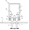
- FIG. 10 shows the structure of a conventional capacitor lead terminal.
- the capacitor lead terminal 5 includes an aluminum wire 2 and a metal wire 3, and the aluminum wire 2 and the metal wire 3 are connected by arc welding or the like.
- the aluminum wire 2 includes a substantially cylindrical round bar portion 2a and a flat portion 2b formed by pressing the round bar portion 2a, and the flat portion 2b of the round bar portion 2a is provided on the flat portion 2b side. Is formed with an inclined portion 2d whose thickness decreases linearly up to the thickness of the flat portion 2b. Furthermore, an electrode foil (not shown) of a capacitor element is connected to the flat portion 2b.
- the electrolytic capacitor 10 includes a capacitor element 9 formed by winding or laminating anode and cathode electrode foils formed of aluminum or the like through a separator together with a driving electrolyte and a bottomed cylindrical exterior.
- the case is housed and the opening formed in the outer case is sealed with a sealing body 8.
- two capacitor lead terminals 5 are inserted into the through holes of the substrate 6 and fixed with solder 7 from the back surface of the substrate 6.
- the capacitor lead terminal 5 is connected to the bus bar, thereby making electrical connection with other electronic components and the like.
- the metal wire 3 of the capacitor lead terminal 5 is fixed to the substrate 6 with the solder 7, and thus vibrates in the direction of the arrow F in the same manner. . Therefore, the round bar portion 2a of the aluminum wire 2 connected to the metal wire 3 by arc welding or the like also vibrates in the direction of the arrow F. Therefore, the flat part 2b of the aluminum wire 2 connected to the electrode foil of the capacitor element 9 vibrates in the direction of the arrow f starting from the boundary part 2e between the round bar part 2a and the flat part 2b.
- the tensile stress and the compressive stress act alternately as a bending moment on the boundary portion 2e that is the starting point of vibration, and the continuous vibration may cause metal fatigue and breakage due to fatigue failure.
- the present invention has been proposed in order to solve such a problem, and even when vibration is continuously applied to the capacitor mounted on the substrate, it does not easily break, has excellent vibration resistance and life characteristics, and
- An object of the present invention is to provide a capacitor lead terminal that can be manufactured at low cost.
- a capacitor lead terminal includes an aluminum wire having a round bar portion and a flat portion, a metal wire connected to the round bar portion of the aluminum wire, the round bar portion, and the And an inclined portion including at least a curved portion at a boundary portion with the flat portion, and a curvature radius R of the curved portion is 0.5 or more.
- At least a curved portion formed in a curved shape is provided at a boundary portion between a round bar portion and a flat portion of an aluminum wire, and the curvature lead R of the curved portion is 0.5 or more. Since the terminal is used, even if vibration is continuously applied to the capacitor, it does not easily break and has excellent vibration resistance and life characteristics. In addition, since it can be manufactured by simply changing the mold during pressing, it is advantageous from the viewpoint of cost.
- the top view of the lead terminal for capacitors concerning one embodiment of the present invention The enlarged view of the curved part of the lead terminal for capacitors concerning this embodiment.
- the perspective view of the lead terminal for capacitors of the present invention when the boundary part of an inclined part and a flat part is made into a straight line.
- the top view of the lead terminal for capacitors of the present invention when the boundary part of an inclined part and a flat part is made into a straight line.
- the perspective view of the lead terminal for capacitors of the present invention when the boundary part of an inclined part and a flat part is made into an arc.
- the top view of the lead terminal for capacitors of the present invention when the boundary part of an inclined part and a flat part is made into a circular arc.
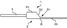
- FIG. 1 shows a capacitor lead terminal according to an embodiment of the present invention.
- the capacitor lead terminal 1 includes an aluminum wire 2 and a metal wire 3, and the aluminum wire 2 and the metal wire 3 are connected by arc welding or the like.
- the aluminum wire 2 includes a substantially cylindrical round bar portion 2a and a flat portion 2b formed by pressing the round bar portion 2a.
- the round bar portion 2a and the flat portion 2b In the boundary portion, an inclined portion 2d whose thickness decreases linearly and a curved portion 2c formed in a curved shape are formed.
- the flat portion 2b is formed by compressing and deforming one end of the aluminum wire 2 by a predetermined length by pressing or the like. On the other hand, a portion where the press working or the like is not performed becomes a round bar portion 2a.
- the flat part 2b is thinner than the round bar part 2a and has a wider shape.
- the flat portion 2b is a portion to which the capacitor electrode foil is connected.
- the metal wire 3 extends to a predetermined length from one end opposite to the side where the flat portion 2b is formed.
- the end surface of the round bar 2a and the end surface of the metal wire 3 are in contact with each other, and both are connected by arc welding or the like.
- a copper-coated steel wire (CP wire) whose surface is generally plated with lead, tin or the like can be used.
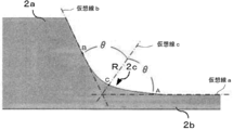
- FIG. 2 shows an enlarged view of the curved portion 2c of the capacitor lead terminal according to the present embodiment.
- the radius of curvature R can be determined as follows. (1) A line parallel to the surface of the flat portion 2b is defined as a virtual line a. (2) A virtual line b is drawn by drawing a straight line transitioning from the round bar part 2a to the flat part 2b. (3) A virtual line c that bisects the angle formed by the virtual line a and the virtual line b is drawn from the intersection of the virtual line a and the virtual line b, and the intersection with the surface of the bending portion 2c is defined as C. (4) When a virtual circle is drawn from the start and end B and the intersection C of the curve, the radius of the virtual circle becomes the curvature radius R.
- the radius of curvature R of the curved portion 2c can be greatly improved by setting the radius of curvature R to 0.5 or more from the results of Examples described later.
- the upper limit of the radius of curvature R is not particularly limited, but is preferably up to 2.0 from the dimensions and strength of the capacitor element product. The larger the radius of curvature R, the longer the curved portion 2c.
- the curved portion 2c is not suitable for a connection portion with the electrode foil because the surface is curved and recessed.
- the capacitor lead terminal 1 is passed through the through hole provided in the sealing body to integrate the sealing body and the capacitor element. However, the curved portion 2c of the capacitor lead terminal 1 is recessed from the surface of the round bar portion 2a.
- the bending part 2c is arrange
- the curved portion 2c can be formed by compressing and deforming by pressing using a mold having a predetermined shape, similarly to the flat portion 2a.
- the boundary portion 2e serving as the boundary between the inclined portion 2d and the flat portion 2b can be a line including a straight line and a curved line in plan view of the flat portion 2b. 3 to 6, an inclined portion 2d is formed across the round bar portion 2a and the flat portion 2b.
- the starting end A of the curved part 2c formed on the flat part 2b be the front-end
- the flat portion 2b and the inclined portion 2d are viewed from above (as viewed from the direction of the arrow X in FIGS.
- the boundary portion 2e can be linear or arcuate. 3 and 4, a boundary portion 2e between the inclined portion 2d and the flat portion 2c is formed in a straight line in a plan view of the flat portion 2b, and FIGS. 5 and 6 illustrate a boundary portion between the inclined portion 2d and the flat portion 2c.
- the boundary portion 2e between the inclined portion 2d and the flat portion 2c is formed as an arc in a plan view of the flat portion 2b, so that a bending moment applied to the boundary portion 2e of the capacitor lead terminal during vibration is obtained. Can be effectively dispersed. Further, it is desirable that the diameter L2 of the arc is 60% or more of the diameter L1 of the round bar portion 2a. If it is less than 60%, the stress dispersion effect may be reduced.
- the capacitor lead terminal 1 presses the aluminum wire 2 with a die having a predetermined shape, and simultaneously forms a round bar portion 2a, a flat portion 2b, a curved portion 2c having a predetermined curvature radius R, and an inclined portion 2d. After the formation, the metal wire 3 can be brought into contact with the end surface of the round bar portion 2a opposite to the flat portion 2b and connected by arc welding or the like.
- the curved portion 2c formed in a curved shape is provided at the boundary portion between the round bar portion 2a and the flat portion 2b of the aluminum wire 2, so that vibration It is possible to disperse stress as a bending moment that is sometimes applied, and to delay fatigue failure due to vibration. Furthermore, the following effects can be achieved.
- the vibration resistance can be improved by, for example, (a) increasing the thickness of the lead terminal and (b) increasing the width, but the following problems arise.
- the connection between the lead terminal 1 and the electrode foil 12 is performed by cold welding in which the lead foil 1 is pressed from the side of the electrode foil 12 with a pressing die, the thickness of the flat portion 2b of the lead terminal 1 is t1. Since the pressing force to the connection part of the pressing die used for cold pressure welding is weakened when the pressure increases from t to t2, the connection strength may be weakened.
- the vibration resistance can be improved without deteriorating the connectivity with the electrode foil 12 as described above.
- the vibration resistance can be improved while suppressing the occurrence of cracking of the electrode foil as described above.
- the vibration resistance of the capacitor lead terminal can be further improved by appropriately selecting the shape of the inclined portion 2d. That is, as shown in FIGS. 5 and 6, when the boundary portion 2e is an arc in plan view on the flat portion 2c, the stress applied to the boundary portion 2e can be radially distributed even if vibration is applied. , Vibration resistance is improved.
- the metal wire 3 is connected after the flat portion 2b and the curved portion 2c are formed on the round bar portion 2a.
- the timing is not limited to this.
- the flat portion 2b and the curved portion 2c may be formed by pressing after connecting the metal wire 3 to the round bar portion 2a. By doing in this way, the metal wire 3 can be grasped at the time of press working for forming the curved portion 2 c on the capacitor lead terminal 1 or when the capacitor lead terminal 1 is moved.
- the round bar part 2a is gripped, the surface of the round bar part 2a may be damaged when gripped.
- the metal wire 3 is connected in advance as a portion to be gripped by the round bar portion 2a.
- the capacitor lead terminal 1 can be manufactured without gripping the round bar portion 2a, and adhesion between the round bar portion 2a and the sealing body 8 can be realized.
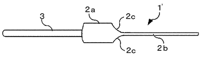
- the flat portion 2b is crushed only from one direction and the curved portion 2c is formed only on one side, but as shown in FIG. 8, it is crushed so as to sandwich the round bar portion 2a, It is good also as a capacitor
- the inclined portion 2d in the side view of the capacitor lead terminal of FIGS. 3 to 6, the inclined portion 2d is linearly reduced in thickness by the inclined portion 2d from the upper side of the round bar portion 2a.
- the present invention is not limited to this.
- the inclined portion 2d in the side view of the capacitor lead terminal, is formed from the position displaced from the upper side of the round bar portion 2a to the flat portion 2b side of the round bar portion 2a without starting the inclined portion 2d from the upper side. Also good. That is, a line may be extended perpendicularly to the flat portion 2b direction from the upper side of the round bar portion 2a, and the inclined portion 2d may be shifted from the line.
- the curvature radius R is set to 0.5 or more, the stress applied to the boundary portion can be remarkably reduced even when a vertical stress is applied to the capacitor lead terminal, and the vibration resistance is improved. To do. Furthermore, when the boundary portion 2e is formed to include an arc, stress as a bending moment applied to the boundary portion from the horizontal direction during vibration can be effectively dispersed.
- a round bar with a diameter of 1.9mm made of aluminum of 99% purity and tempered F material is prepared and pressed to form a flat shape with a width of 1.98mm and a thickness of 0.27mm as shown in FIG.
- a capacitor lead terminal 1 having a curved portion 2c having a portion 2a and a radius of curvature R of 0.50 mm was formed as Example 1.
- a capacitor lead terminal 5 having a shape with a radius of curvature R of 0 at the boundary portion as shown in FIG.
- Example 1 the lead terminals of Example 1 and the conventional example were used and applied to a capacitor element having a product size of ⁇ 16 ⁇ 20 Lmm, and then a vibration test was performed to determine whether or not the lead terminal was broken.
- the conditions of the vibration test are as follows. Frequency: 50, 100, 2000Hz Acceleration: 20G when frequency is 50Hz, 40G when frequency is 100Hz and 2000Hz Sweep speed: 0.5 oct / min Vibration test time: 6.6 hours to 11546 hours for each of the three directions of the X axis, Y axis, and Z axis Test sample c: Four in each direction Test environment: Room temperature
- the sweep speed refers to the speed at which the frequency and acceleration are continuously changed.
- the point of 50 Hz and 20G is point A
- the point of 40G is point B
- the point of 2000 Hz and 40G is point C
- a ⁇ B ⁇ C ⁇ B ⁇ A ⁇ B ⁇ C It means that the speed is changed continuously in a cycle of ⁇ B ⁇ A...
- the speed between the points is set as 0.5 oct / min.
- the parallel direction to the imaginary line connecting the capacitor lead terminals 5 is the X axis
- the vertical direction is the Y axis
- the vertical direction is the Z axis.
- Example 1 when the vibration time was 2523 hours, one sample was broken on the X axis, and when the vibration time was 11546 hours, only one sample was broken on the Y axis. there were. From these results, the vibration time in which the vibration resistance is recognized as good in Example 1 is determined to be up to 2523 hours.
- Example 2 a round bar having a purity of 99% and a tempered F material made of aluminum and having a diameter of 1.9 mm was prepared and subjected to press working to obtain a shape having a width of 1.
- the vibration resistance ratio was 1.77 times that of the sample of the conventional example. This value is considered to be a level that does not deviate from the error range as compared with the value of the conventional example. According to the above results, it is considered that the radius of curvature R is preferably 0.5 or more.
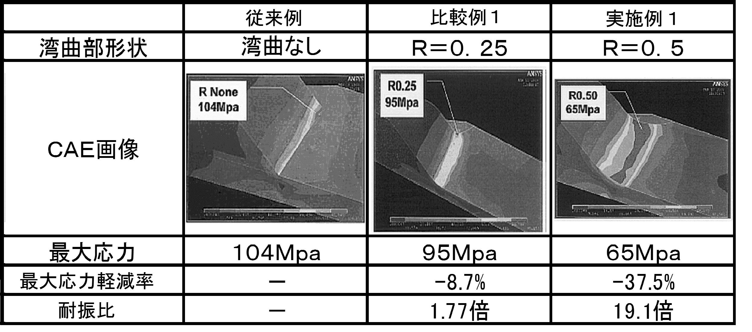
- CAE analysis CAE analysis was performed on the samples of Example 1, Comparative Example 1, and the conventional example, and the maximum stress was measured.
- CAE analysis Computer Aided Engineering
- the maximum stress reduction rate is a ratio obtained by dividing the value obtained by subtracting the maximum stress of the conventional example from the maximum stress of the target sample by the maximum stress of the conventional example.
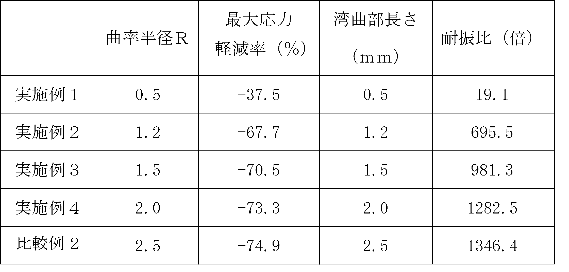
- Example 2 (Changes the radius of curvature R) Further, the shape shown in FIG. 1 except that the radius of curvature R is 1.2 mm (Example 2), 1.5 mm (Example 3), 2 mm (Example 4), and 2.5 mm (Comparative Example 2).
- a capacitor lead terminal 1 was formed under the same conditions as in Example 1.
- the maximum stress reduction rate and vibration resistance of the samples of Examples 2 to 4 and Comparative Example 2 were evaluated in the same manner as the vibration test of Example 1 described above. The results are shown in Table 3.
- the vibration resistance ratios of Examples 2 to 4 and Comparative Example 2 were calculated in the same manner as in Example 1.
- Fig. 9 shows a graph of the vibration resistance ratio in Table 3. It can be seen that when the radius of curvature R exceeds 2.0, the difference in the effect of the maximum stress reduction rate becomes small. On the other hand, the larger the radius of curvature R, the longer the curved portion 2c. The length of the curved portion 2c leads to an increase in space that does not contribute to the capacity in the case, and affects the volume efficiency of the capacitor. Therefore, the radius of curvature R is desirably 2.0 or less.
- Capacitor lead terminal 2 Aluminum wire 2a ... Round bar part 2b ... Flat part 2c ... Curved part 2d ... Inclined part 2e ... Boundary part 3 ... Metal wire 5 . Capacitor lead terminal 6 ... Substrate 7 ... Solder 8 ... Sealing body 9 ... Capacitor element 10 ... Electrolytic capacitor 12 ... Electrode foil 13 ... Stitch needle 14a ... Long leaf 14b ... Short leaf
Landscapes
- Engineering & Computer Science (AREA)
- Power Engineering (AREA)
- Microelectronics & Electronic Packaging (AREA)
- Chemical & Material Sciences (AREA)
- Chemical Kinetics & Catalysis (AREA)
- Electrochemistry (AREA)
- Electric Double-Layer Capacitors Or The Like (AREA)
- Fixed Capacitors And Capacitor Manufacturing Machines (AREA)
Abstract
基板に実装されたコンデンサに振動が継続的に加えられても、破断が起こりにくく、耐振性や寿命特性に優れ、かつ安価に製造可能なコンデンサ用リード端子を提供する。コンデンサ用リード端子1は、丸棒部2a及び平坦部2bを有するアルミニウム線2と、アルミニウム線2の丸棒部2aに溶接された金属線3とを有する。さらに、コンデンサ用リード端子1は、丸棒部2aと平坦部2bとの境界部分に、湾曲状に形成された湾曲部2cを有し、湾曲部2cの曲率半径Rは0.5以上に設定されている。
Description
本発明は、コンデンサ素子に接続されるコンデンサ用リード端子に関する。
近年、自動車の電子化が進み、コンデンサが車載装置に使用される機会が増えており、車載装置の基板やモジュールのバスバーにコンデンサ用リード端子を介して接続されている。車載装置では、走行時の路面からの振動及びエンジン等の回転による振動等が継続的にモジュールや基板に加えられる。そのため、モジュールや基板に実装されたコンデンサにも継続的な振動が加えられる。その結果、コンデンサのリード端子が破断するといった不具合が生じることがある。
図10に、従来のコンデンサ用リード端子の構造を示す。
コンデンサ用リード端子5は、アルミニウム線2と金属線3とから構成されており、アルミニウム線2と金属線3とはアーク溶接等で接続されている。また、アルミニウム線2は、略円柱形状の丸棒部2aと、この丸棒部2aがプレス加工等されて形成された平坦部2bとを備えており、丸棒部2aの平坦部2b側には、平坦部2bの厚みまで直線的に厚みが減少する傾斜部2dが形成されている。さらに、平坦部2bには、コンデンサ素子の電極箔(図示せず)が接続される。
コンデンサ用リード端子5は、アルミニウム線2と金属線3とから構成されており、アルミニウム線2と金属線3とはアーク溶接等で接続されている。また、アルミニウム線2は、略円柱形状の丸棒部2aと、この丸棒部2aがプレス加工等されて形成された平坦部2bとを備えており、丸棒部2aの平坦部2b側には、平坦部2bの厚みまで直線的に厚みが減少する傾斜部2dが形成されている。さらに、平坦部2bには、コンデンサ素子の電極箔(図示せず)が接続される。
上記のような構造を有するコンデンサ用リード端子5を電解コンデンサに用いた場合に、振動のストレスによって破断に至るメカニズムについて、図11を参照して説明する。
図11に示すように、電解コンデンサ10は、アルミニウム等で形成された陽極および陰極の電極箔をセパレータを介して巻回又は積層したコンデンサ素子9を、駆動用電解液とともに有底筒状の外装ケースに収納し、この外装ケースに形成された開口を封口体8で密封して形成されている。また、電解コンデンサ10では、2本のコンデンサ用リード端子5が基板6のスルーホールに挿入され、基板6の裏面から半田7で固定されている。
また、モジュールにおいては、コンデンサ用リード端子5がバスバーに接続されることで、他の電子部品等と電気的接続を成している。
この基板6が基板表面と平行な矢印Fの方向に振動した場合、コンデンサ用リード端子5の金属線3は、基板6に半田7で固定されているため、同様に矢印Fの方向に振動する。よって、金属線3にアーク溶接等で接続されているアルミニウム線2の丸棒部2aも同様に矢印Fの方向に振動することとなる。その為、コンデンサ素子9の電極箔に接続されているアルミニウム線2の平坦部2bは、丸棒部2aと平坦部2bの境界部2eを起点に、矢印fの方向に振動する。
その結果、振動の起点となる境界部2eは、集中的に引っ張り応力と圧縮応力が曲げモーメントとして交互に働き、継続的な振動によっては金属疲労を起こし、疲労破壊による破断を引き起こす場合がある。
このような振動に対する耐振性に優れたコンデンサとして、コンデンサのケース開口部を封口するための封口体8とコンデンサ素子9の密着性を高めて、コンデンサ素子9の移動を防止する構成が提案されている(例えば、特許文献1参照)。また、封口体8と基板6の間に突片を設け、コンデンサ自体の振動を抑えるといった提案もされている(例えば、特許文献2参照)。
しかしながら、このような提案においても耐振性は未だ充分とはいえず、さらなる特性の向上が望まれていた。また、これらの提案は、コンデンサ素子に構造的な変更を加えて振動を防止するものであるので、製造に用いる既存の設備を変更する必要があり、コストが増大するという不利益もあった。
耐振性を向上させる他の方法として、固定剤によりコンデンサ素子を固定する方法もあるが、コンデンサ素子の固定を強固に行うには、ケース内に充填する固定剤の量を多くしなければならない。このため、コンデンサの使用時に内圧が上昇した場合等にケース内の許容空間が小さくなって、圧力弁等の安全装置が作動し易くなり、コンデンサの寿命を短くしてしまうという課題があった。また、固定剤の種類によっては、高温度下で軟化し、固定性が悪化してしまう。これに対し、高温度対応可能なシリコン系の固定剤を用いた場合には、シロキ酸結合により発生したガスがコンデンサ内の圧力を上昇させ、圧力弁等の安全装置を作動させるという課題があった。
さらに、ケース側面を加締めて素子を固定する方法もあるが、コンデンサの封止とは別にケース側面を加締める工程が必要となるため、加工費が掛かり、単価が上がってしまうという課題があった。
本発明はこのような課題を解決するために提案されたものであり、基板に実装されたコンデンサに振動が継続的に加えられても、破断が起こりにくく、耐振性や寿命特性に優れ、かつ安価に製造可能なコンデンサ用リード端子を提供することを目的とする。
上述の目的を達成するため、本発明のコンデンサ用リード端子は、丸棒部及び平坦部を有するアルミニウム線と、該アルミニウム線の丸棒部に接続された金属線と、前記丸棒部と前記平坦部との境界部分に、少なくとも湾曲部を含む傾斜部と、を有し、該湾曲部の曲率半径Rが0.5以上であることを特徴とする。
本発明によれば、アルミニウム線の丸棒部と平坦部との境界部分に、少なくとも湾曲状に形成された湾曲部を設け、該湾曲部の曲率半径Rを0.5以上としたコンデンサ用リード端子を用いているので、コンデンサに振動が継続的に加えられても、破断が起こりにくく、耐振性や寿命特性に優れたものとなる。また、プレス加工の際に型を変えるだけで製造が可能であるため、コスト面からも優位である。
以下、本発明に係るコンデンサ用リード端子の実施形態について、図面を参照しつつ詳細に説明する。
(コンデンサ用リード端子の構造)
図1に、本発明の一実施形態に係るコンデンサ用リード端子を示す。
このコンデンサ用リード端子1は、アルミニウム線2と金属線3とから構成されており、アルミニウム線2と金属線3とはアーク溶接等で接続されている。また、アルミニウム線2は、略円柱形状の丸棒部2aと、この丸棒部2aがプレス加工等されて形成された平坦部2bとを備えており、丸棒部2aと平坦部2bとの境界部分には、直線的に厚みが減少する傾斜部2dと、湾曲状に形成された湾曲部2cとが形成されている。
図1に、本発明の一実施形態に係るコンデンサ用リード端子を示す。
このコンデンサ用リード端子1は、アルミニウム線2と金属線3とから構成されており、アルミニウム線2と金属線3とはアーク溶接等で接続されている。また、アルミニウム線2は、略円柱形状の丸棒部2aと、この丸棒部2aがプレス加工等されて形成された平坦部2bとを備えており、丸棒部2aと平坦部2bとの境界部分には、直線的に厚みが減少する傾斜部2dと、湾曲状に形成された湾曲部2cとが形成されている。
平坦部2bは、アルミニウム線2の一端がプレス加工等で所定の長さだけ圧縮変形されることで形成される。一方、前記プレス加工等がされていない部分が丸棒部2aとなる。平坦部2bは丸棒部2aよりも薄く、幅広な形状を有している。この平坦部2bは、コンデンサの電極箔が接続される部分である。
丸棒部2aにおいて、平坦部2bが形成された方と逆の一端からは、金属線3が所定の長さに延伸している。丸棒部2aの端面と金属線3の端面は当接しており、両者はアーク溶接等で接続されている。
金属線3としては、一般的に鉛や錫等で表面をメッキされた銅被覆鋼線(CP線)が使用され得る。
(湾曲部の曲率半径R)
図2に、本実施形態に係るコンデンサ用リード端子の湾曲部2cの拡大図を示す。
湾曲部2cにおいて、曲率半径Rは、以下のようにして決定することができる。
(1)平坦部2bの面と平行な線を仮想線aとする。
(2)丸棒部2aから平坦部2bへと移行する直線を引いて仮想線bとする。
(3)仮想線aと仮想線bとの交点から、仮想線aと仮想線bとのなす角度を2等分する仮想線cを引き、湾曲部2cの表面との交点をCとする。
(4)曲線の始端Aと終端Bおよび交点Cから仮想円を描くと、その仮想円の半径が曲率半径Rとなる。
図2に、本実施形態に係るコンデンサ用リード端子の湾曲部2cの拡大図を示す。
湾曲部2cにおいて、曲率半径Rは、以下のようにして決定することができる。
(1)平坦部2bの面と平行な線を仮想線aとする。
(2)丸棒部2aから平坦部2bへと移行する直線を引いて仮想線bとする。
(3)仮想線aと仮想線bとの交点から、仮想線aと仮想線bとのなす角度を2等分する仮想線cを引き、湾曲部2cの表面との交点をCとする。
(4)曲線の始端Aと終端Bおよび交点Cから仮想円を描くと、その仮想円の半径が曲率半径Rとなる。
湾曲部2cの曲率半径Rは、後述する実施例の結果から、0.5以上とすることにより、耐振性を大きく向上させることができる。曲率半径Rの上限は特に限定されないが、コンデンサ素子の製品の寸法、強度面から、好ましくは2.0までとする。曲率半径Rが大きいほど、湾曲部2cの長さは長くなる。湾曲部2cは表面が湾曲して窪んでいるため、電極箔との接続箇所には適さない。また、封口体に設けた貫通孔にコンデンサ用リード端子1を貫通させて封口体とコンデンサ素子を一体化しているが、コンデンサ用リード端子1の湾曲部2cは丸棒部2aの表面より窪んでいるため、封口体の貫通孔の内周面と湾曲部2cは密着せず密封性が実現しない。そのため、湾曲部2cは、コンデンサ素子の封口体側の端面と、封口体との間に配置したり、湾曲部2cの長さ分だけ封口体の高さを大きくしたりする。つまり、湾曲部2cの長さが大きくなることで、コンデンサの高さ寸法が大きくなる。そして、曲率半径Rが2.0を超えると、応力低減の効果の差は小さくなる。湾曲部2cの大きさの応力軽減の効果と、コンデンサの高さ方向の高背化を考慮すると湾曲部2cの曲率半径Rは2.0以下が好ましい。
湾曲部2cは、平坦部2aと同様に、所定の形状の型を用いてプレス加工により圧縮変形することで形成できる。
(傾斜部と平坦部の境界部)
本実施形態に係るコンデンサ用リード端子では、傾斜部2dと平坦部2bとの境界となる境界部2eを平坦部2bの平面視で直線及び曲線とを含む線とすることができる。図3~6では、丸棒部2aと平坦部2bとに渡って傾斜部2dが形成される。平坦部2b上に形成される湾曲部2cの始端Aを傾斜部2dの先端とし、この始端Aをつなげた部分を境界部2eとする。この場合、平坦部2bおよび傾斜部2dを上方方向からの上面視(図3および図5中の矢印X方向から視た)で、境界部2eが直線状、または円弧状とすることができる。図3及び図4は、傾斜部2dと平坦部2cとの境界部2eを平坦部2bの平面視で直線で形成し、図5及び図6は、傾斜部2dと平坦部2cとの境界部2eを平坦部2bの平面視で円弧を含み形成した例を示す。
本実施形態に係るコンデンサ用リード端子では、傾斜部2dと平坦部2bとの境界となる境界部2eを平坦部2bの平面視で直線及び曲線とを含む線とすることができる。図3~6では、丸棒部2aと平坦部2bとに渡って傾斜部2dが形成される。平坦部2b上に形成される湾曲部2cの始端Aを傾斜部2dの先端とし、この始端Aをつなげた部分を境界部2eとする。この場合、平坦部2bおよび傾斜部2dを上方方向からの上面視(図3および図5中の矢印X方向から視た)で、境界部2eが直線状、または円弧状とすることができる。図3及び図4は、傾斜部2dと平坦部2cとの境界部2eを平坦部2bの平面視で直線で形成し、図5及び図6は、傾斜部2dと平坦部2cとの境界部2eを平坦部2bの平面視で円弧を含み形成した例を示す。
図5及び図6のように、傾斜部2dと平坦部2cとの境界部2eを平坦部2bの平面視で円弧とすることで、振動時にコンデンサ用リード端子の境界部2eに加わる曲げモーメントとしての応力を効果的に分散することができる。また、円弧の直径L2を丸棒部2aの直径L1の60%以上とすることが望ましい。60%未満となると、応力の分散効果が低減するおそれがある。
(コンデンサ用リード端子の製造方法)
次に、本実施形態に係るコンデンサ用リード端子1の製造方法について説明する。コンデンサ用リード端子1は、アルミニウム線2に対して所定の形状を有する型でプレス加工を行い、丸棒部2a、平坦部2b、所定の曲率半径Rを有する湾曲部2c及び傾斜部2dを同時に形成した後、丸棒部2aの平坦部2bと反対側の端面に金属線3を当接し、アーク溶接等によって接続することによって製造することができる。
次に、本実施形態に係るコンデンサ用リード端子1の製造方法について説明する。コンデンサ用リード端子1は、アルミニウム線2に対して所定の形状を有する型でプレス加工を行い、丸棒部2a、平坦部2b、所定の曲率半径Rを有する湾曲部2c及び傾斜部2dを同時に形成した後、丸棒部2aの平坦部2bと反対側の端面に金属線3を当接し、アーク溶接等によって接続することによって製造することができる。
(効果)
以上のように、本実施形態のコンデンサ用リード端子1では、アルミニウム線2の丸棒部2aと平坦部2bとの境界部分に、湾曲状に形成された湾曲部2cを設けているので、振動時に加えられる曲げモーメントとしての応力を分散することができ、振動による疲労破壊を遅らせることができる。さらに、以下の効果を奏することができる。
以上のように、本実施形態のコンデンサ用リード端子1では、アルミニウム線2の丸棒部2aと平坦部2bとの境界部分に、湾曲状に形成された湾曲部2cを設けているので、振動時に加えられる曲げモーメントとしての応力を分散することができ、振動による疲労破壊を遅らせることができる。さらに、以下の効果を奏することができる。
(1)後述する実施例からも明らかな通り、曲率半径Rを0.5以上とすることによって、境界部分に加わる応力を著しく低減でき、耐振性が約20倍向上する。
(2)特許文献1や特許文献2記載の方法とは異なり、コンデンサ素子に構造的な変更を加えて振動を防止するものではないので、既存の設備を変更することなく製造が可能であり、安価でコスト的に優位である。
(3)耐振性を向上させるには、例えば、リード端子を、(ア)厚くする、(イ)幅広にする、ことによっても可能であるが、以下のような問題が生じる。
(ア)厚くした場合
後述する実施例の表2および表3を参照すると、実施例1のコンデンサ用リード端子1の平坦部2bの厚みt1を0.27mmとした場合、最大応力軽減率は-37.5%となる。この最大応力軽減率と同等の値を従来のコンデンサ用リード端子5の構造を用いて達成するためには、別の実験結果より平坦部2bの厚みt2を0.43mmまで厚くする必要があった。
後述する実施例の表2および表3を参照すると、実施例1のコンデンサ用リード端子1の平坦部2bの厚みt1を0.27mmとした場合、最大応力軽減率は-37.5%となる。この最大応力軽減率と同等の値を従来のコンデンサ用リード端子5の構造を用いて達成するためには、別の実験結果より平坦部2bの厚みt2を0.43mmまで厚くする必要があった。
しかしながら、平坦部2bの厚みを大きくすると、電極箔との接続性が悪化するという問題が生じる。
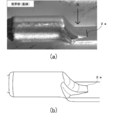
即ち、図7(a)に示すように、リード端子1を電極箔12に固定する際、リード端子1の平坦部2bを電極箔12と重ねて、両者にステッチ針13を貫通させ、電極箔12の裏面から突出した長尺リーフ14aの部分を折り返して電極箔12に挟み込むことによって固定している。ここで、リード端子1の平坦部2bの厚みがt1からt2に大きくなると、図7(b)に示すように、ステッチ針13を同じ位置まで貫通させても電極箔12の裏面から突出するリーフは短尺リーフ14bとなり、折り返し部分が少なくなって充分に固定することができなくなってしまう。
即ち、図7(a)に示すように、リード端子1を電極箔12に固定する際、リード端子1の平坦部2bを電極箔12と重ねて、両者にステッチ針13を貫通させ、電極箔12の裏面から突出した長尺リーフ14aの部分を折り返して電極箔12に挟み込むことによって固定している。ここで、リード端子1の平坦部2bの厚みがt1からt2に大きくなると、図7(b)に示すように、ステッチ針13を同じ位置まで貫通させても電極箔12の裏面から突出するリーフは短尺リーフ14bとなり、折り返し部分が少なくなって充分に固定することができなくなってしまう。
また、リード端子1と電極箔12との接続を、リード端子1に重ねた電極箔12側から押圧金型で押圧する冷間圧接による場合においても、リード端子1の平坦部2bの厚みがt1からt2に大きくなると、冷間圧接に用いる押圧金型の接続箇所への押圧力が弱まるため、接続強度が弱くなる場合がある。
これに対して、本実施形態のコンデンサ用リード端子1を用いれば、上記のような電極箔12との接続性が悪化することなく、耐振性を向上させることができる。
(イ)幅広にした場合
後述する実施例を参照すると、実施例1のコンデンサ用リード端子1の平坦部2bの幅を1.98mmとした場合、最大応力軽減率は-37.5%となる。この最大応力軽減率と同等の値を従来のコンデンサ用リード端子5の構造を用いて達成するためには、別の実験結果より平坦部2bの幅を2.50mmまで広げる必要があった。
後述する実施例を参照すると、実施例1のコンデンサ用リード端子1の平坦部2bの幅を1.98mmとした場合、最大応力軽減率は-37.5%となる。この最大応力軽減率と同等の値を従来のコンデンサ用リード端子5の構造を用いて達成するためには、別の実験結果より平坦部2bの幅を2.50mmまで広げる必要があった。
しかしながら、巻回型素子の場合、リード端子の幅を広げると、素子が楕円形となってケース空間の体積効率が悪化するとともに、リード端子の角部に配置される電極箔の曲率がきつくなり、電極箔の割れが生じるおそれがある。
従って、本実施形態のコンデンサ用リード端子1を用いれば、上記のような電極箔の割れの発生を抑制しつつ、耐振性を向上させることができる。
(4)また、本実施形態では、傾斜部2dの形状を適宜選択することにより、コンデンサ用リード端子の耐振性をより向上させることが可能となる。すなわち、図5及び図6のように、境界部2eを平坦部2c上の平面視で円弧とした場合には、振動が加わっても境界部2eに加わる応力を放射状に分散することが可能となり、耐振動性が向上する。
(他の実施形態)
上記の実施形態では、丸棒部2aに平坦部2bと湾曲部2cを形成後に金属線3を接続したが、このようなタイミングに限るものではない。例えば、丸棒部2aに金属線3を接続後、プレス加工によって平坦部2bと湾曲部2cを形成してもよい。このようにすることで、コンデンサ用リード端子1に湾曲部2cを形成するプレス加工の際や、コンデンサ用リード端子1を移動させる際に金属線3を把持することができる。丸棒部2aを把持した場合、丸棒部2aの表面に把持した際の傷がつく場合がある。この傷により封口体8の貫通孔表面と丸棒部2aとの密着性が低下し、電解液等が漏れることがあるが、丸棒部2aに把持する部位として予め金属線3を接続することで、丸棒部2aを把持することなく、コンデンサ用リード端子1の製造が可能となり、丸棒部2aと封口体8との密着性を実現できる。
上記の実施形態では、丸棒部2aに平坦部2bと湾曲部2cを形成後に金属線3を接続したが、このようなタイミングに限るものではない。例えば、丸棒部2aに金属線3を接続後、プレス加工によって平坦部2bと湾曲部2cを形成してもよい。このようにすることで、コンデンサ用リード端子1に湾曲部2cを形成するプレス加工の際や、コンデンサ用リード端子1を移動させる際に金属線3を把持することができる。丸棒部2aを把持した場合、丸棒部2aの表面に把持した際の傷がつく場合がある。この傷により封口体8の貫通孔表面と丸棒部2aとの密着性が低下し、電解液等が漏れることがあるが、丸棒部2aに把持する部位として予め金属線3を接続することで、丸棒部2aを把持することなく、コンデンサ用リード端子1の製造が可能となり、丸棒部2aと封口体8との密着性を実現できる。
また、上記の実施の形態では、平坦部2bは、一方方向からのみ潰し、湾曲部2cは片面のみに形成しているが、図8に示すように、丸棒部2aを挟むように潰し、丸棒部2aの直径方向の中心から平坦部2bを形成し、湾曲部2cを2箇所形成したコンデンサ用リード端子1’としてもよい。
また、本実施形態では、傾斜部2dの形状の一例として図3~6のコンデンサ用リード端子の側面図において、傾斜部2dが丸棒部2aの上辺より傾斜部2dにより直線的に厚みが減少した例を示したがこれに限らない。例えば、コンデンサ用リード端子の側面図において、傾斜部2dの開始箇所を丸棒部2aの上辺からとせず、丸棒部2aの平坦部2b側に変位させた位置から傾斜部2dを形成しても良い。すなわち、丸棒部2aの上辺より平坦部2b方向に垂直に線を伸ばし、その線上より傾斜部2dに移行しても良い。この場合にでも、曲率半径Rを0.5以上とすることによって、コンデンサ用リード端子に対して垂直方向の応力が加わった場合にでも、境界部に加わる応力を著しく低減でき、耐振性が向上する。更に、境界部2eを円弧を含み形成すると、振動時に水平方向から境界部分に加わる曲げモーメントとしての応力を効果的に分散することができる。
次に、本発明の実施例について従来例及び比較例と対比して説明することにより、本発明の効果を実証する。
(振動試験)
純度99%、調質F材のアルミニウムからなる直径1.9mmの丸棒を用意し、プレス加工を施して、図1に示すような形状で、幅1.98mm、厚さ0.27mmの平坦部2a及び曲率半径Rが0.50mmの湾曲部2cを有するコンデンサ用リード端子1を形成して実施例1とした。
純度99%、調質F材のアルミニウムからなる直径1.9mmの丸棒を用意し、プレス加工を施して、図1に示すような形状で、幅1.98mm、厚さ0.27mmの平坦部2a及び曲率半径Rが0.50mmの湾曲部2cを有するコンデンサ用リード端子1を形成して実施例1とした。
一方、図10に示すような境界部分の曲率半径Rが0である形状で、平坦部2aが同様の寸法を有するコンデンサ用リード端子5を形成して従来例とした。
次に、実施例1及び従来例のリード端子を用い、製品サイズがφ16×20Lmmのコンデンサ素子に適用した後、振動試験を行い、リード端子の破断の有無を判定した。振動試験の条件は、以下の通りである。
周波数:50、100、2000Hz
加速度:周波数が50Hzのとき20G、100Hz及び2000Hzのとき40G
掃引速度:0.5oct/分
振動試験時間:X軸、Y軸、Z軸の3方向各6.6時間~11546時間
試験サンプルc:各方向で4個
試験環境:常温
周波数:50、100、2000Hz
加速度:周波数が50Hzのとき20G、100Hz及び2000Hzのとき40G
掃引速度:0.5oct/分
振動試験時間:X軸、Y軸、Z軸の3方向各6.6時間~11546時間
試験サンプルc:各方向で4個
試験環境:常温
上記振動実験の条件において、掃引速度とは、周波数と加速度の各ポイントへ連続的に変化させる速度をいう。つまり、50Hz、20GのポイントをポイントA、100Hz、40GのポイントをポイントB、2000Hz、40GのポイントをポイントCとした場合、周波数と加速度について、A→B→C→B→A→B→C→B→A・・・というサイクルで連続的に変化させ、その変化の速度として、各ポイント間の速度を0.5oct/分と設定したことを意味する。
また、上記振動実験の振動方向において、図11のようにコンデンサを基板に固定した場合、コンデンサ用リード端子5同士を結ぶ仮想線と平行方向をX軸、垂直方向をY軸とし、コンデンサの高さ方向をZ軸とする。
振動試験の結果を表1に示す。

上記表において、「c=0」は、振動試験後に壊れたサンプル数が0個、「c=1」は、1個、「c=2」は、2個であることを示す。
振動実験の結果、従来例では、振動時間が132時間の場合にY軸で破断したサンプルが1個生じ、振動時間が198時間の場合にX軸で破断したサンプルが1個生じた。その後も、振動時間が790時間の場合にX軸で破断したサンプルが1個生じ、Y軸で破断したサンプルが2個生じた。さらに、振動時間が887時間の場合にX軸で破断したサンプルが1個生じ、振動時間が1849時間の場合にY軸及びZ軸で破断したサンプルが各1個生じ、振動時間が2523時間の場合にX軸で破断したサンプルが1個生じた。これらの結果より、従来例において耐振性が良好であると認められる振動時間は、132時間までと判定される。
これに対して、実施例1では、振動時間が2523時間の場合にX軸で破断したサンプルが1個生じ、振動時間が11546時間の場合にY軸で破断したサンプルが1個生じたのみであった。これらの結果より、実施例1において耐振性が良好であると認められる振動時間は、2523時間までと判定される。
以上の結果より、実施例1のサンプルは、従来例のサンプルと比較して、耐振比が2523/132=19.1倍も向上していることが判明した。
さらに、実施例1と同様に、純度99%、調質F材のアルミニウムからなる直径1.9mmの丸棒を用意し、プレス加工を施して、図1に示すような形状で、幅1.98mm、厚さ0.27mmの平坦部2a及び曲率半径Rが0.25mmの湾曲部2cを有するコンデンサ用リード端子を形成し比較例1とした。
上述した実施例1の振動試験と同様にして比較例1のサンプルについて耐振性を評価した結果、耐振比は従来例のサンプルと比較して1.77倍であった。この値は、従来例の値と比較して誤差範囲を逸脱しない程度と考えられる。
以上の結果によれば、曲率半径Rは0.5以上とすることが好ましいと考えられる。
以上の結果によれば、曲率半径Rは0.5以上とすることが好ましいと考えられる。
(CAE解析)
上記の実施例1、比較例1および従来例のサンプルに対して、CAE解析を行い、最大応力を測定した。
ここで、CAE解析(Computer Aided Engineering)とは、コンデンサ用リード端子1を構成するアルミニウムの物性や、大きさ等の形状、平坦部2bを平面上から押圧する力の大きさを設定することで、境界部に加わる応力を算出するシミュレーションである。
上記の実施例1、比較例1および従来例のサンプルに対して、CAE解析を行い、最大応力を測定した。
ここで、CAE解析(Computer Aided Engineering)とは、コンデンサ用リード端子1を構成するアルミニウムの物性や、大きさ等の形状、平坦部2bを平面上から押圧する力の大きさを設定することで、境界部に加わる応力を算出するシミュレーションである。
各サンプルについてのCAE画像、最大応力、最大応力軽減率および耐振比の結果について、表2にまとめて示す。
最大応力軽減率は、対象となるサンプルの最大応力から従来例の最大応力を減じた値を従来例の最大応力で割った割合である。
表2の結果より、湾曲部2cの曲率半径Rを0.5とすることによって、応力の分散が認められて最大応力が65Mpaとなり、従来例と比較して応力が-37.5%軽減され、結果として耐振性が約20倍向上することが分かった。
(曲率半径Rを変化)
さらに、図1に示す形状で、曲率半径Rが1.2mm(実施例2)、1.5mm(実施例3)、2mm(実施例4)、2.5mm(比較例2)とした以外は実施例1と同様の条件でコンデンサ用リード端子1を形成した。上述した実施例1の振動試験と同様にして実施例2~4および比較例2のサンプルについて最大応力軽減率および耐振性について評価した。結果を表3に示す。なお、各実施例2~4および比較例2の耐振比は、実施例1と同様に算出した。
さらに、図1に示す形状で、曲率半径Rが1.2mm(実施例2)、1.5mm(実施例3)、2mm(実施例4)、2.5mm(比較例2)とした以外は実施例1と同様の条件でコンデンサ用リード端子1を形成した。上述した実施例1の振動試験と同様にして実施例2~4および比較例2のサンプルについて最大応力軽減率および耐振性について評価した。結果を表3に示す。なお、各実施例2~4および比較例2の耐振比は、実施例1と同様に算出した。
表3の結果より、曲率半径Rが増大するにつれて最大応力軽減率および耐振比が共に向上することが判明した。
表3の耐振比をグラフ化したものを図9に示す。曲率半径Rが2.0を超えると、最大応力軽減率の効果の差が小さくなることが分かる。一方で、曲率半径Rを大きくするほど、湾曲部2cが長くなる。湾曲部2cの長さは、ケース内の容量に寄与しない空間の増加につながり、コンデンサの体積効率に影響する。そのため、曲率半径Rは2.0以下が望ましい。
1、1’…コンデンサ用リード端子
2…アルミニウム線
2a…丸棒部
2b…平坦部
2c…湾曲部
2d…傾斜部
2e…境界部
3…金属線
5…コンデンサ用リード端子
6…基板
7…半田
8…封口体
9…コンデンサ素子
10…電解コンデンサ
12…電極箔
13…ステッチ針
14a…長尺リーフ
14b…短尺リーフ
2…アルミニウム線
2a…丸棒部
2b…平坦部
2c…湾曲部
2d…傾斜部
2e…境界部
3…金属線
5…コンデンサ用リード端子
6…基板
7…半田
8…封口体
9…コンデンサ素子
10…電解コンデンサ
12…電極箔
13…ステッチ針
14a…長尺リーフ
14b…短尺リーフ
Claims (4)
- 丸棒部及び平坦部を有するアルミニウム線と、
該アルミニウム線の丸棒部に溶接された金属線と、
前記丸棒部と前記平坦部との境界部分に、少なくとも湾曲部を含む傾斜部と、を
有し、
該湾曲部の曲率半径Rが0.5以上であることを特徴とするコンデンサ用リード端子。 - 前記曲率半径Rが2.0以下であることを特徴とする請求項1記載のコンデンサ用リード端子。
- 前記傾斜部と前記平坦部との境界部は、平坦部の上面視で円弧を含むことを特徴とする請求項1または請求項2に記載のコンデンサ用リード端子。
- 前記境界部を形成する円弧の直径は、前記丸棒部の直径の60%以上であることを特徴する請求項3に記載のコンデンサ用リード端子。
Priority Applications (2)
| Application Number | Priority Date | Filing Date | Title |
|---|---|---|---|
| JP2016510562A JPWO2015147286A1 (ja) | 2014-03-27 | 2015-03-27 | コンデンサ用リード端子 |
| US15/275,467 US9905366B2 (en) | 2014-03-27 | 2016-09-25 | Lead terminal for capacitor |
Applications Claiming Priority (2)
| Application Number | Priority Date | Filing Date | Title |
|---|---|---|---|
| JP2014066078 | 2014-03-27 | ||
| JP2014-066078 | 2014-03-27 |
Related Child Applications (1)
| Application Number | Title | Priority Date | Filing Date |
|---|---|---|---|
| US15/275,467 Continuation US9905366B2 (en) | 2014-03-27 | 2016-09-25 | Lead terminal for capacitor |
Publications (1)
| Publication Number | Publication Date |
|---|---|
| WO2015147286A1 true WO2015147286A1 (ja) | 2015-10-01 |
Family
ID=54195790
Family Applications (1)
| Application Number | Title | Priority Date | Filing Date |
|---|---|---|---|
| PCT/JP2015/059698 Ceased WO2015147286A1 (ja) | 2014-03-27 | 2015-03-27 | コンデンサ用リード端子 |
Country Status (3)
| Country | Link |
|---|---|
| US (1) | US9905366B2 (ja) |
| JP (1) | JPWO2015147286A1 (ja) |
| WO (1) | WO2015147286A1 (ja) |
Cited By (2)
| Publication number | Priority date | Publication date | Assignee | Title |
|---|---|---|---|---|
| KR20170105411A (ko) * | 2016-03-09 | 2017-09-19 | 고호꾸고오교오가부시끼가이샤 | 전해 콘덴서용의 리드선 단자, 전해 콘덴서 및 전해 콘덴서의 제조 방법 |
| CN107180701A (zh) * | 2016-03-09 | 2017-09-19 | 湖北工业株式会社 | 电解电容器用引线端子、电解电容器以及电解电容器的制造方法 |
Citations (5)
| Publication number | Priority date | Publication date | Assignee | Title |
|---|---|---|---|---|
| JPH0229517U (ja) * | 1989-07-15 | 1990-02-26 | ||
| JPH07130576A (ja) * | 1993-10-28 | 1995-05-19 | Nippon Chemicon Corp | コンデンサ素子用端子リードの製造方法 |
| JP2001210551A (ja) * | 2000-01-27 | 2001-08-03 | Aputodeito:Kk | 電解コンデンサ用タブ端子 |
| JP2003217972A (ja) * | 2002-01-18 | 2003-07-31 | Matsushita Electric Ind Co Ltd | 外部引き出し用リード線及びこれを用いたコンデンサ |
| JP2013143556A (ja) * | 2012-01-12 | 2013-07-22 | Nippon Chemicon Corp | コンデンサ用リード端子及びその製造方法 |
Family Cites Families (8)
| Publication number | Priority date | Publication date | Assignee | Title |
|---|---|---|---|---|
| US4037142A (en) * | 1976-01-29 | 1977-07-19 | Sprague Electric Company | Electrolytic capacitor package having a grommet with tapered lead holes |
| JPH06176975A (ja) * | 1992-12-07 | 1994-06-24 | Elna Co Ltd | 電解コンデンサおよびそのタブ端子 |
| JP2000315632A (ja) * | 1999-03-02 | 2000-11-14 | Matsushita Electric Ind Co Ltd | コンデンサ |
| JP2003257799A (ja) | 2002-02-28 | 2003-09-12 | Sanyo Electric Co Ltd | 固体電解コンデンサ |
| JP2004104013A (ja) * | 2002-09-12 | 2004-04-02 | Nichicon Corp | 電解コンデンサ |
| JP2009277748A (ja) | 2008-05-13 | 2009-11-26 | Rubycon Corp | コンデンサ |
| CN103392214B (zh) * | 2011-02-18 | 2016-08-17 | 松下知识产权经营株式会社 | 电解电容器及其制造方法 |
| CN107103999B (zh) * | 2012-04-27 | 2019-07-16 | 爱尔那株式会社 | 铝电解电容器及其封口橡胶 |
-
2015
- 2015-03-27 JP JP2016510562A patent/JPWO2015147286A1/ja active Pending
- 2015-03-27 WO PCT/JP2015/059698 patent/WO2015147286A1/ja not_active Ceased
-
2016
- 2016-09-25 US US15/275,467 patent/US9905366B2/en active Active
Patent Citations (5)
| Publication number | Priority date | Publication date | Assignee | Title |
|---|---|---|---|---|
| JPH0229517U (ja) * | 1989-07-15 | 1990-02-26 | ||
| JPH07130576A (ja) * | 1993-10-28 | 1995-05-19 | Nippon Chemicon Corp | コンデンサ素子用端子リードの製造方法 |
| JP2001210551A (ja) * | 2000-01-27 | 2001-08-03 | Aputodeito:Kk | 電解コンデンサ用タブ端子 |
| JP2003217972A (ja) * | 2002-01-18 | 2003-07-31 | Matsushita Electric Ind Co Ltd | 外部引き出し用リード線及びこれを用いたコンデンサ |
| JP2013143556A (ja) * | 2012-01-12 | 2013-07-22 | Nippon Chemicon Corp | コンデンサ用リード端子及びその製造方法 |
Cited By (7)
| Publication number | Priority date | Publication date | Assignee | Title |
|---|---|---|---|---|
| KR20170105411A (ko) * | 2016-03-09 | 2017-09-19 | 고호꾸고오교오가부시끼가이샤 | 전해 콘덴서용의 리드선 단자, 전해 콘덴서 및 전해 콘덴서의 제조 방법 |
| CN107180701A (zh) * | 2016-03-09 | 2017-09-19 | 湖北工业株式会社 | 电解电容器用引线端子、电解电容器以及电解电容器的制造方法 |
| JP2017168810A (ja) * | 2016-03-09 | 2017-09-21 | 湖北工業株式会社 | 電解コンデンサ用のリード線端子、電解コンデンサ及び電解コンデンサの製造方法 |
| KR20190072506A (ko) * | 2016-03-09 | 2019-06-25 | 고호꾸고오교오가부시끼가이샤 | 전해 콘덴서용의 리드선 단자, 전해 콘덴서 및 전해 콘덴서의 제조 방법 |
| CN110223843A (zh) * | 2016-03-09 | 2019-09-10 | 湖北工业株式会社 | 电解电容器用引线端子、及电解电容器 |
| KR102209009B1 (ko) | 2016-03-09 | 2021-01-28 | 고호꾸고오교오가부시끼가이샤 | 전해 콘덴서용의 리드선 단자, 전해 콘덴서 및 전해 콘덴서의 제조 방법 |
| KR102209007B1 (ko) * | 2016-03-09 | 2021-01-28 | 고호꾸고오교오가부시끼가이샤 | 전해 콘덴서용의 리드선 단자, 전해 콘덴서 및 전해 콘덴서의 제조 방법 |
Also Published As
| Publication number | Publication date |
|---|---|
| US20170011859A1 (en) | 2017-01-12 |
| US9905366B2 (en) | 2018-02-27 |
| JPWO2015147286A1 (ja) | 2017-04-13 |
Similar Documents
| Publication | Publication Date | Title |
|---|---|---|
| US10468204B2 (en) | Capacitor and manufacturing method therefor | |
| JP2013191832A (ja) | 積層セラミック電子部品 | |
| US11017956B2 (en) | Capacitor and method for manufacturing same | |
| CN103177880A (zh) | 固态电解电容器以及制造固态电解电容器的方法 | |
| CN105469995B (zh) | 固体电解电容器 | |
| WO2015147286A1 (ja) | コンデンサ用リード端子 | |
| JP4782044B2 (ja) | チップ形アルミニウム電解コンデンサ | |
| KR102209009B1 (ko) | 전해 콘덴서용의 리드선 단자, 전해 콘덴서 및 전해 콘덴서의 제조 방법 | |
| US9595394B2 (en) | Solid electrolytic capacitor, anode lead connection method for the same, and production method for solid electrolytic capacitor | |
| JP6880772B2 (ja) | コンデンサおよびその製造方法 | |
| JP6019588B2 (ja) | コンデンサ用リード端子及びその製造方法 | |
| JP6503672B2 (ja) | コンデンサの製造方法 | |
| JP2019067939A (ja) | コンデンサおよびその製造方法 | |
| JP2018152483A (ja) | コンデンサおよびその製造方法 | |
| JP5119083B2 (ja) | チップ形電解コンデンサ | |
| JP7668367B2 (ja) | コンデンサ | |
| JP7833676B2 (ja) | 電解コンデンサおよびその製造方法 | |
| JP2005101480A (ja) | リードフレームを具えた電子部品 | |
| JP6354450B2 (ja) | コンデンサおよびその製造方法 | |
| CN107180701A (zh) | 电解电容器用引线端子、电解电容器以及电解电容器的制造方法 | |
| JP2016046387A (ja) | コンデンサ | |
| JP2013089737A (ja) | 電解コンデンサおよびその製造方法 | |
| JP2005216880A (ja) | コンデンサ |
Legal Events
| Date | Code | Title | Description |
|---|---|---|---|
| 121 | Ep: the epo has been informed by wipo that ep was designated in this application |
Ref document number: 15768044 Country of ref document: EP Kind code of ref document: A1 |
|
| ENP | Entry into the national phase |
Ref document number: 2016510562 Country of ref document: JP Kind code of ref document: A |
|
| NENP | Non-entry into the national phase |
Ref country code: DE |
|
| 122 | Ep: pct application non-entry in european phase |
Ref document number: 15768044 Country of ref document: EP Kind code of ref document: A1 |