WO2015146593A1 - 磁気センサおよび磁気センサの製造方法ならびに電流センサ - Google Patents
磁気センサおよび磁気センサの製造方法ならびに電流センサ Download PDFInfo
- Publication number
- WO2015146593A1 WO2015146593A1 PCT/JP2015/057200 JP2015057200W WO2015146593A1 WO 2015146593 A1 WO2015146593 A1 WO 2015146593A1 JP 2015057200 W JP2015057200 W JP 2015057200W WO 2015146593 A1 WO2015146593 A1 WO 2015146593A1
- Authority
- WO
- WIPO (PCT)
- Prior art keywords
- layer
- magnetic
- magnetic layer
- free
- magnetization
- Prior art date
Links
Images


Classifications
-
- G—PHYSICS
- G01—MEASURING; TESTING
- G01R—MEASURING ELECTRIC VARIABLES; MEASURING MAGNETIC VARIABLES
- G01R33/00—Arrangements or instruments for measuring magnetic variables
- G01R33/02—Measuring direction or magnitude of magnetic fields or magnetic flux
- G01R33/06—Measuring direction or magnitude of magnetic fields or magnetic flux using galvano-magnetic devices
- G01R33/09—Magnetoresistive devices
- G01R33/091—Constructional adaptation of the sensor to specific applications
-
- G—PHYSICS
- G01—MEASURING; TESTING
- G01R—MEASURING ELECTRIC VARIABLES; MEASURING MAGNETIC VARIABLES
- G01R15/00—Details of measuring arrangements of the types provided for in groups G01R17/00 - G01R29/00, G01R33/00 - G01R33/26 or G01R35/00
- G01R15/14—Adaptations providing voltage or current isolation, e.g. for high-voltage or high-current networks
- G01R15/20—Adaptations providing voltage or current isolation, e.g. for high-voltage or high-current networks using galvano-magnetic devices, e.g. Hall-effect devices, i.e. measuring a magnetic field via the interaction between a current and a magnetic field, e.g. magneto resistive or Hall effect devices
- G01R15/205—Adaptations providing voltage or current isolation, e.g. for high-voltage or high-current networks using galvano-magnetic devices, e.g. Hall-effect devices, i.e. measuring a magnetic field via the interaction between a current and a magnetic field, e.g. magneto resistive or Hall effect devices using magneto-resistance devices, e.g. field plates
-
- G—PHYSICS
- G01—MEASURING; TESTING
- G01R—MEASURING ELECTRIC VARIABLES; MEASURING MAGNETIC VARIABLES
- G01R19/00—Arrangements for measuring currents or voltages or for indicating presence or sign thereof
- G01R19/0092—Arrangements for measuring currents or voltages or for indicating presence or sign thereof measuring current only
-
- G—PHYSICS
- G01—MEASURING; TESTING
- G01R—MEASURING ELECTRIC VARIABLES; MEASURING MAGNETIC VARIABLES
- G01R3/00—Apparatus or processes specially adapted for the manufacture or maintenance of measuring instruments, e.g. of probe tips
-
- G—PHYSICS
- G01—MEASURING; TESTING
- G01R—MEASURING ELECTRIC VARIABLES; MEASURING MAGNETIC VARIABLES
- G01R33/00—Arrangements or instruments for measuring magnetic variables
- G01R33/0052—Manufacturing aspects; Manufacturing of single devices, i.e. of semiconductor magnetic sensor chips
-
- G—PHYSICS
- G01—MEASURING; TESTING
- G01R—MEASURING ELECTRIC VARIABLES; MEASURING MAGNETIC VARIABLES
- G01R33/00—Arrangements or instruments for measuring magnetic variables
- G01R33/02—Measuring direction or magnitude of magnetic fields or magnetic flux
- G01R33/06—Measuring direction or magnitude of magnetic fields or magnetic flux using galvano-magnetic devices
- G01R33/09—Magnetoresistive devices
- G01R33/093—Magnetoresistive devices using multilayer structures, e.g. giant magnetoresistance sensors
-
- H—ELECTRICITY
- H10—SEMICONDUCTOR DEVICES; ELECTRIC SOLID-STATE DEVICES NOT OTHERWISE PROVIDED FOR
- H10N—ELECTRIC SOLID-STATE DEVICES NOT OTHERWISE PROVIDED FOR
- H10N50/00—Galvanomagnetic devices
- H10N50/01—Manufacture or treatment
-
- H—ELECTRICITY
- H10—SEMICONDUCTOR DEVICES; ELECTRIC SOLID-STATE DEVICES NOT OTHERWISE PROVIDED FOR
- H10N—ELECTRIC SOLID-STATE DEVICES NOT OTHERWISE PROVIDED FOR
- H10N50/00—Galvanomagnetic devices
- H10N50/10—Magnetoresistive devices
-
- H—ELECTRICITY
- H10—SEMICONDUCTOR DEVICES; ELECTRIC SOLID-STATE DEVICES NOT OTHERWISE PROVIDED FOR
- H10N—ELECTRIC SOLID-STATE DEVICES NOT OTHERWISE PROVIDED FOR
- H10N50/00—Galvanomagnetic devices
- H10N50/80—Constructional details
-
- H—ELECTRICITY
- H10—SEMICONDUCTOR DEVICES; ELECTRIC SOLID-STATE DEVICES NOT OTHERWISE PROVIDED FOR
- H10N—ELECTRIC SOLID-STATE DEVICES NOT OTHERWISE PROVIDED FOR
- H10N50/00—Galvanomagnetic devices
- H10N50/80—Constructional details
- H10N50/85—Magnetic active materials
Definitions
- the present invention relates to a magnetic sensor, a method for manufacturing the magnetic sensor, and a current sensor including the magnetic sensor.
- a current sensor capable of measuring a large current without contact is required.
- a sensor using a magnetic sensor that detects an induced magnetic field from a current to be measured is known.
- the magnetic detection element for the magnetic sensor include a magnetoresistive effect element such as a GMR element.
- the GMR element has a basic structure of a laminated structure in which a fixed magnetic layer and a free magnetic layer are laminated via a nonmagnetic material layer.
- the pinned magnetic layer has an exchange coupling bias due to a laminated structure of an antiferromagnetic layer and a ferromagnetic layer, and an RKKY interaction (indirect exchange mutual interaction) due to a self-pinned structure in which two ferromagnetic layers are laminated via a nonmagnetic intermediate layer. (Operation), the magnetization direction is fixed in one direction.
- the free magnetic layer can change the magnetization direction in accordance with an external magnetic field.
- an induced magnetic field from a current to be measured is applied to the GMR element, whereby the magnetization direction of the free magnetic layer changes. Since the electric resistance value of the GMR element varies depending on the relationship between the magnetization direction of the free magnetic layer and the magnetization direction of the pinned magnetic layer, the magnetization direction of the free magnetic layer can be detected by measuring the electric resistance value. Can do. Based on the magnetization direction detected by the magnetic sensor, it is possible to determine the magnitude and direction of the current to be measured to which the induced magnetic field is applied.
- a current sensor using a magnetic sensor is required to increase the measurement accuracy of the magnetic sensor so that the current value can be detected more accurately.
- it is required to realize a reduction in offset, a reduction in output signal variation, an improvement in linearity (output linearity), and the like.
- One preferable means for meeting these requirements is to reduce the hysteresis of the GMR element included in the magnetic sensor.
- a bias magnetic field is applied to the free magnetic layer so that the magnetization direction of the free magnetic layer is aligned even when no induced magnetic field from the current to be measured is applied. It is done.
- Patent Document 1 discloses a method of providing a hard bias layer made of a permanent magnet. Further, in Patent Document 2, an anti-ferromagnetic layer capable of causing an exchange coupling bias with a free magnetic layer and aligning the magnetization direction of the free magnetic layer in a predetermined direction in a state where the magnetization can be varied is used as the free magnetic layer. A method of laminating is disclosed.
- the present invention provides a magnetic sensor and a magnetic sensor capable of reducing hysteresis of a magnetoresistive effect element while using a single magnetic domain of a free magnetic layer based on an exchange coupling bias disclosed in Patent Document 2 as a basic technology. It is an object of the present invention to provide a method and a current sensor using a magnetic sensor.
- an external magnetic field such as an induced magnetic field from a current to be measured (in this specification, an external magnetic field to be measured is also referred to as a “magnetic field to be measured”) is applied to the free magnetic layer by an exchange coupling bias.
- the magnetization direction based on the exchange coupling bias generated in the free magnetic layer is also referred to as “initial magnetization direction”
- a component orthogonal to the initial magnetization direction of the residual magnetization in the free magnetic layer is also referred to as “residual orthogonal component”).
- residual orthogonal component By applying a magnetic field having an antiparallel component to the orthogonal component from the outside, the residual orthogonal component can be reduced.
- the magnetization direction of the free magnetic layer is affected by the measured magnetic field from the initial magnetization direction. Receive and rotate. By measuring the variation of the element resistance value based on this magnetization rotation, the magnitude and direction of the magnetic field to be measured can be detected. However, even after the application of the magnetic field to be measured is completed, the magnetization direction of the free magnetic layer does not completely return to the initial magnetization direction, and a component orthogonal to the initial magnetization direction remains in the magnetization direction of the free magnetic layer. This contributes to the hysteresis of the magnetoresistive effect element.
- the magnetic field applied to the free magnetic layer for this purpose is also referred to as “hysteresis canceling magnetic field” or “HC magnetic field”.
- the hard bias layer is often a basic laminated structure of a magnetoresistive effect element (seed layer / fixed magnetic layer / nonmagnetic). Therefore, the positional relationship between the hard bias layer and the free magnetic layer is likely to vary, and the magnitude and direction of the HC magnetic field may vary.
- a ferromagnetic layer in this specification, “hysteresis cancel layer” or It was found that the HC magnetic field can be efficiently applied to the free magnetic layer by laminating the “HC layer”.
- an exchange coupling bias with the antiferromagnetic layer is generated in the HC layer as in the free magnetic layer.
- the magnetization direction of the HC layer also rotates due to the influence of the magnetic field to be measured.
- magnetization having a component orthogonal to the magnetization direction based on the exchange coupling bias remains. Therefore, by setting the magnetization direction based on the exchange coupling bias with the antiferromagnetic layer in the HC layer to be equal to the initial magnetization direction in the free magnetic layer, the reflux magnetic field based on the remanent magnetization of the HC layer is changed to the free magnetic layer.
- the free magnetic layer It is possible to act on the free magnetic layer as an external magnetic field having a component antiparallel to the residual orthogonal component. As a result, the residual orthogonal component of the free magnetic layer is reduced, and the hysteresis of the GMR element can be reduced.
- the temperature dependence of the reflux magnetic field applied from the HC layer to the free magnetic layer has the same basic tendency as the temperature dependence of the magnitude of the exchange coupling bias between the free magnetic layer and the antiferromagnetic layer.
- the HC layer also functions as a temperature compensation mechanism for the magnetoresistive effect element, and can reduce fluctuations caused by temperature changes in the measured values of the magnetic sensor.
- an exchange coupling bias is generated between the free magnetic layer and the side opposite to the nonmagnetic material layer, and the magnetization direction of the free magnetic layer can be varied.
- An antiferromagnetic layer that can be aligned in a predetermined direction is provided, and an exchange coupling bias between the antiferromagnetic layer and the side opposite to the free magnetic layer in the antiferromagnetic layer is provided.
- a magnetization direction based on the exchange coupling bias generated in the free magnetic layer is provided in the ferromagnetic layer.
- the resulting exchange The magnetization direction is the same as the magnetization direction based on a coupling bias, and the ferromagnetic layer is capable of applying a reflux magnetic field having a component in a direction along the sensitivity axis to the free magnetic layer.
- the magnitude of the exchange coupling bias generated in the ferromagnetic layer and the thickness of the ferromagnetic layer are set so as to reduce the component in the direction along the sensitivity axis of the remanent magnetization of the free magnetic layer.
- a first magnetic layer and a second magnetic layer in contact with the nonmagnetic material layer are laminated via a nonmagnetic intermediate layer, and the first magnetic layer and the second magnetic layer are The magnetic sensor according to any one of (1) to (3), wherein the magnetic sensor is a self-pinning type in which magnetization is fixed in antiparallel.
- the magnitude of the exchange coupling bias generated in the ferromagnetic layer and the thickness of the ferromagnetic layer are set so as to reduce the high temperature storage time dependency of the sensitivity of the free magnetic layer (1) ) To (4).
- a method of manufacturing a magnetic sensor comprising a step of laminating a seed layer, a pinned magnetic layer, a nonmagnetic material layer, a free magnetic layer, an antiferromagnetic layer, and a ferromagnetic layer in this order on a substrate, the laminating direction
- a first magnetic layer is stacked on the seed layer while applying a magnetic field in a first direction orthogonal to the first layer, and then a nonmagnetic intermediate layer and a second magnetic layer are sequentially stacked to provide a self-pinned structure.
- a method of manufacturing a magnetic sensor comprising: a free layer stacking step of sequentially stacking the free magnetic layer, the antiferromagnetic layer, and the ferromagnetic layer on the nonmagnetic material layer while applying a magnetic field.
- the structure of the ferromagnetic layer is set so that a reflux magnetic field in a direction parallel to the first direction can be applied from the ferromagnetic layer to the free magnetic layer.
- a current sensor including the magnetic sensor according to any one of (1) to (5) above.
- a magnetic sensor capable of reducing the hysteresis of the magnetoresistive effect element.
- a method for manufacturing the magnetic sensor and a current sensor using the magnetic sensor are also provided.
- FIG. 2 is a cross-sectional view taken along the line II-II shown in FIG. It is a graph which shows the design stripe width dependence of zero magnetic field hysteresis. It is a graph which shows the sensitivity dependence of zero magnetic field hysteresis. It is a graph which shows the dependence with respect to the change rate of the magnitude
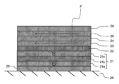
- FIG. 1 is a conceptual diagram (plan view) of a magnetic sensor according to an embodiment of the present invention
- FIG. 2 is a cross-sectional view taken along line II-II shown in FIG.
- the magnetic sensor 1 includes a stripe-shaped magnetoresistive element 11 as shown in FIG.
- the magnetoresistive element 11 has a plurality of strip-like long patterns 12 (stripes) arranged so that the stripe longitudinal direction D1 (hereinafter also simply referred to as “longitudinal direction D1”) is parallel to each other. And has a shape (a meander shape).
- the sensitivity axis direction is a direction D2 orthogonal to the longitudinal direction D1 of the long pattern 12 (hereinafter also simply referred to as “width direction D2”). Accordingly, when the magnetic sensor 1 including the meander-shaped magnetoresistive element 11 is used, the magnetic field to be measured and the canceling magnetic field are applied along the width direction D2.
- each of the long patterns 12 other than those located at the end portion in the arrangement direction is the other strip-like long portion closest to the end portion.
- the pattern 12 and the conductive portion 13 are connected.
- the long pattern 12 positioned at the end in the arrangement direction is connected to the connection terminal 14 via the conductive portion 13.
- the magnetoresistive effect element 11 has a configuration in which the plurality of long patterns 12 are connected in series by the conductive portion 13 between the two connection terminals 14 and 14.
- the conductive portion 13 and the connection terminal 14 may be nonmagnetic or magnetic, but are preferably made of a material with low electrical resistance.
- the magnetic sensor 1 can output signals from the magnetoresistive effect element 11 from the two connection terminals 14 and 14.
- a signal from the magnetoresistive effect element 11 output from the connection terminals 14 and 14 is input to a calculation unit (not shown), and the measurement unit calculates power to be measured based on the signal.
- each of the long patterns 12 of the magnetoresistive effect element 11 is formed on the chip 29 from below through an insulating layer (not shown), from the seed layer 20, the fixed magnetic layer 21, the nonmagnetic material.
- the layer 22, the free magnetic layer 23, the antiferromagnetic layer 24, the HC layer 25, and the protective layer 26 are stacked in this order.
- the method for forming these layers is not limited.
- the film may be formed by sputtering.
- the seed layer 20 is formed of NiFeCr or Cr.
- the pinned magnetic layer 21 has a self-pinned structure of a first magnetic layer 21a, a second magnetic layer 21c, and a nonmagnetic intermediate layer 21b located between the first magnetic layer 21a and the second magnetic layer 21c.
- the fixed magnetization direction of the first magnetic layer 21a and the fixed magnetization direction of the second magnetic layer 21c are antiparallel.
- the fixed magnetization direction of the second magnetic layer 21c is the fixed magnetization direction in the fixed magnetic layer 21, that is, the sensitivity axis direction.
- the first magnetic layer 21a is formed on the seed layer 20, and the second magnetic layer 21c is formed in contact with a nonmagnetic material layer 22 described later.
- the first magnetic layer 21a in the present embodiment is preferably formed of a FeCo alloy that is a higher coercive force material than the second magnetic layer 21c.
- the second magnetic layer 21c in contact with the nonmagnetic material layer 22 is a layer that contributes to the magnetoresistance effect (specifically, the GMR effect), and the second magnetic layer 21c has conduction electrons having up spins and down spins.
- a magnetic material that can increase the mean free path difference of conduction electrons is selected.
- the difference in the magnetization amount (saturation magnetization Ms and film thickness t) between the first magnetic layer 21a and the second magnetic layer 21c is adjusted to be substantially zero.
- the pinned magnetic layer 21 in this embodiment has a self-pinned structure, it does not include an antiferromagnetic layer. Thereby, the temperature characteristic of the magnetoresistive effect element 11 is not restricted by the blocking temperature of the antiferromagnetic layer.
- the coercive force Hc of the first magnetic layer 21a is increased, and the difference in magnetization between the first magnetic layer 21a and the second magnetic layer 21c is adjusted to substantially zero.
- the nonmagnetic material layer 22 is made of Cu (copper) or the like.
- the free magnetic layer 23 shown in FIG. 2 has a single layer structure such as NiFe or CoFe or a laminated structure, but is not limited thereto.
- the material constituting the protective layer 26 is not limited. Examples include Ta (tantalum).
- an antiferromagnetic layer 24 is formed on the upper surface of the free magnetic layer 23.
- the antiferromagnetic layer 24 is preferably formed of IrMn that can generate an exchange coupling bias (exchange coupling magnetic field; Hex) without performing an annealing process in the magnetic field with the free magnetic layer 23.
- an exchange coupling bias exchange coupling magnetic field; Hex
- an annealing process in a magnetic field is required. It is preferable not to use PtMn or NiMn.
- the thickness of the antiferromagnetic layer 24 and the magnitude of the exchange coupling bias generated in the free magnetic layer 23 are limited as long as the magnetization direction of the free magnetic layer 23 can be aligned in a state in which the magnetization can be varied with respect to the magnetic field to be measured.
- the film thickness of the antiferromagnetic layer 24 is about 40 to 80 mm.
- the magnitude of the exchange coupling bias generated in the free magnetic layer 23 is about 50 to 300 Oe (about 4 kA / m to about 24 kA / m).
- the magnetization direction F of the free magnetic layer in FIG. 2 indicates the initial magnetization direction, and the magnetization direction F of the free magnetic layer 23 is relative to the fixed magnetization direction of the fixed magnetic layer 21 (the fixed magnetization direction of the second magnetic layer 21c). They are aligned in the orthogonal direction.
- the antiferromagnetic layer 24 is formed on the entire upper surface of the free magnetic layer 23, but the present invention is not limited to this, and a defective portion may be formed in a part of the antiferromagnetic layer 24.
- the antiferromagnetic layer 24 is formed on the entire surface of the free magnetic layer 23, the entire free magnetic layer 23 can be appropriately single-domained in one direction and the hysteresis can be further reduced, so that the measurement accuracy can be improved. This is preferable.
- the magnetoresistive element 11 has an antiferromagnetic layer on the side opposite to the side facing the free magnetic layer 23 in the antiferromagnetic layer 24, that is, on the upper surface side of the antiferromagnetic layer 24 in FIG. 2.
- An HC layer 25 is provided in which an exchange coupling bias is generated between the magnetic layer 24 and the magnetization direction thereof can be aligned in a predetermined direction in a state where the magnetization can be varied.
- the HC layer 25 is a ferromagnetic layer made of a ferromagnetic material so that an exchange coupling bias can be appropriately generated between the HC layer 25 and the antiferromagnetic layer 24.
- the exchange coupling bias generated in the free magnetic layer 23 due to the antiferromagnetic layer 24 is opposite to the exchange coupling bias generated in the HC layer 25 due to the antiferromagnetic layer 24 so that the magnetization directions are equal.
- the ferromagnetic layer 24 and the HC layer 25 are set. Further, the HC layer 25 can apply a reflux magnetic field having a component in the direction along the sensitivity axis, that is, the width direction D2, to the free magnetic layer 23. If the magnetoresistive effect element 11 is configured to include a plurality of long patterns 12 spaced apart from each other as shown in FIG.
- the HC layer 25 has a special structure such as extremely thin, Usually, it is easy to give the component in the direction along the sensitivity axis in the reflux magnetic field from the HC layer 25 to the free magnetic layer 23.
- the component along the sensitivity axis in the reflux magnetic field from the HC layer 25 is also referred to as “reflux orthogonal component”.
- the magnetization direction of the HC layer 25 rotates along the direction of the measured magnetic field such as an induced magnetic field from the measured current, similarly to the free magnetic layer 23, the magnetization direction of the HC layer 25 is from the HC layer 25 applied to the free magnetic layer 23.
- the return quadrature component is opposite to the direction of the magnetic field to be measured. Therefore, when the application of the magnetic field to be measured is completed and a residual orthogonal component exists in the free magnetic layer 23, the return orthogonal component based on the residual magnetization of the HC layer 25 is the residual orthogonal component of the free magnetic layer 23. This is in the opposite direction to the component and acts to erase the residual orthogonal component of the free magnetic layer 23. Therefore, the magnetoresistive effect element 11 according to one embodiment of the present invention is likely to reduce hysteresis.
- the material constituting the HC layer 25 is not limited as long as it is a ferromagnetic material.
- examples of such materials include NiFeNb materials, NiFe materials, and CoFe materials.
- a material having a relatively high volume resistivity such as a NiFeNb-based material for the HC layer 25.
- the HC layer 25 may have a single layer structure or a laminated structure.
- the HC layer 25 has a laminated structure and a NiFe-based material on the antiferromagnetic layer 24
- a relatively thin layer made of a material that easily generates an exchange coupling bias as described above is positioned in contact with the antiferromagnetic layer 24, and is relatively distal to the antiferromagnetic layer 24. It is preferable to locate a relatively thick layer of a material having a relatively high volume resistivity, such as a system material.
- the linearity of the magnetic sensor including the magnetoresistive effect element 11 can be improved by adjusting the composition and thickness of each layer. Further, the linearity of the magnetic sensor including the magnetoresistive effect element 11 can be improved by annealing the magnetoresistive effect element 11 including the HC layer 25 (application of a magnetic field is not necessary in this annealing process). Sometimes you can.
- the HC layer 25 can also function as a temperature compensation mechanism for the magnetoresistive effect element 11 as described below.
- the exchange coupling bias generated between the antiferromagnetic layer 24 and the free magnetic layer 23 and the HC layer 25 has a high temperature due to various factors (composition variation, bonding interface mismatch, mutual diffusion, etc.). As a basic tendency, the exchange coupling bias increases as the storage time in a high-temperature environment increases.
- the exchange coupling bias generated in the HC layer 25 is basically the same as the exchange coupling bias generated in the free magnetic layer 23. Therefore, the reflux magnetic field from the HC layer 25 becomes larger as the storage time in the high temperature environment is shorter, and becomes smaller as the storage time in the high temperature environment is longer.
- the reflux orthogonal component from the HC layer 25 that acts to lower the magnetization rotation angle is relatively large.
- the reflux orthogonal component from the HC layer 25 that acts to lower the magnetization rotation angle is relatively small.
- the change in the magnetization rotation of the free magnetic layer 23 based on the change in the storage time in the high temperature environment is less likely to occur, and the variation in the measurement value due to the storage time in the high temperature environment is less likely to occur.
- the configuration (composition, thickness, etc.) of the HC layer 25 may be set appropriately.
- the HC layer 25 is formed over the entire upper surface of the antiferromagnetic layer 24, but the present invention is not limited to this, and a defective portion may be formed in a part of the HC layer 25. However, it is preferable that the HC layer 25 is formed on the entire surface of the antiferromagnetic layer 24 because the residual orthogonal component of the free magnetic layer 23 can be appropriately reduced and the measurement accuracy can be improved.
- Method for Manufacturing Magnetic Sensor A method for manufacturing a magnetic sensor according to an embodiment of the present invention is not limited. According to the method described below, the magnetic sensor according to this embodiment can be efficiently manufactured.
- a seed layer 20 is formed on a substrate 29 via an insulating layer (not shown in FIG. 2), and a pinned magnetic layer 21 having a self-pinning structure is laminated thereon.
- a first magnetic layer 21a, a nonmagnetic intermediate layer 21b, and a second magnetic layer 21c are sequentially stacked as shown in FIG.
- the film forming means for each layer is not limited. Sputtering is exemplified. If the first magnetic layer 21a is magnetized along the width direction D2 in FIG. 1 by applying a magnetic field when forming the first magnetic layer 21a, the second magnetic layer 21c is caused by the RKKY interaction. Can be strongly magnetized in a direction antiparallel to the magnetization direction of the first magnetic layer 21a. The second magnetic layer 21c magnetized in this way can maintain a state magnetized in the width direction D2 without being affected by a magnetic field having a direction different from its magnetization direction in a subsequent manufacturing process. Is possible.
- a nonmagnetic material layer 22 is laminated on the pinned magnetic layer 21.
- the method for stacking the nonmagnetic material layer 22 is not limited, and a specific example is sputtering.
- the free magnetic layer 23, the antiferromagnetic layer 24, and the HC layer 25 are sequentially stacked on the nonmagnetic material layer 22 while applying a magnetic field in the direction along the longitudinal direction D1.
- the method for laminating these layers is not limited, and a specific example is sputtering.
- an exchange coupling bias is generated between the antiferromagnetic layer 24 in the direction along the magnetization direction of the free magnetic layer 23, and in the direction equal to the magnetization direction of the free magnetic layer 23.
- an exchange coupling bias is generated between the magnetized HC layer 25 and the antiferromagnetic layer 24 in the direction along the magnetization direction.
- the free magnetic layer 23 and the HC layer 25 are in the same direction in the longitudinal direction D1 due to the exchange coupling bias generated between the antiferromagnetic layer 24.
- a magnetic field is also applied to the fixed magnetic layer 21, but the fixed magnetic layer 21 has a pinning structure based on the RKKY interaction, so Does not change the magnetization direction.
- the material constituting the antiferromagnetic layer 24 when an IrMn-based material is used as the material constituting the antiferromagnetic layer 24, it is possible to align the magnetization direction of the antiferromagnetic layer 24 by film formation in a magnetic field without special heat treatment. is there. Therefore, it is possible to make the process in which the annealing process in the magnetic field is not performed throughout the process of manufacturing the magnetoresistive effect element 11.
- the magnetoresistive effect element 11 having different sensitivity axes (including the case where the magnetization directions are opposite to each other) on the same substrate by making the manufacturing process of the magnetoresistive effect element 11 an annealing free process in a magnetic field as described above. Can be easily manufactured.
- the manufacturing process of the magnetoresistive effect element 11 requires annealing in the magnetic field, if the annealing in the magnetic field is performed a plurality of times, the effect of the annealing in the magnetic field previously performed is reduced, and the magnetization direction is appropriately set. May be difficult to do.
- the protective layer 26 is finally stacked.
- the method for laminating the protective layer 26 is not limited, and a specific example is sputtering.
- Removal processing is performed on the laminated structure obtained by the above film forming process, and a plurality of long patterns 12 are arranged in the width direction D2.
- a conductive portion 13 for connecting the plurality of long patterns 12 and a connection terminal 14 for connecting to the conductive portion 13 are formed to obtain the magnetoresistive element 11 having a meander shape shown in FIG.
- a magnetic sensor including a magnetoresistive effect element according to an embodiment of the present invention can be suitably used as a current sensor.
- Such a current sensor may have a configuration including one magnetoresistive effect element, but as described in Patent Document 1 and Patent Document 2, it is preferable to use four elements and build a bridge circuit to improve measurement accuracy.
- the method for manufacturing a magnetoresistive element according to an embodiment of the present invention does not include annealing in a magnetic field, and therefore it is easy to manufacture a plurality of magnetoresistive elements on the same substrate.
- a magnetic proportional current sensor is a magnetoresistive effect element according to an embodiment of the present invention (a magnetoresistive effect element having a laminated structure in which a pinned magnetic layer and a free magnetic layer are laminated via a nonmagnetic material layer).
- an exchange coupling bias is generated between the free magnetic layer and the magnetization direction of the free magnetic layer is aligned in a predetermined direction so that the magnetization can be varied.
- An antiferromagnetic layer is provided, and an exchange coupling bias is generated between the antiferromagnetic layer and the side opposite to the free magnetic layer in the antiferromagnetic layer, and the magnetization direction can be varied.
- a ferromagnetic layer that can be aligned in a predetermined direction is provided, and the magnetization direction based on the exchange coupling bias generated in the free magnetic layer is the same direction as the magnetization direction based on the exchange coupling bias generated in the ferromagnetic layer.
- the ferromagnetic layer is configured to include at least one magnetoresistive element capable of applying a reflux magnetic field having a component in the direction along the sensitivity axis to the free magnetic layer.
- a magnetic field detection bridge circuit having two outputs that generate a voltage difference according to the induced magnetic field from the current is provided.
- the current to be measured is measured by the potential difference output from the magnetic field detection bridge circuit according to the induced magnetic field.
- a magnetic balance type current sensor includes at least one magnetoresistive effect element according to an embodiment of the present invention, and includes a magnetic field detection bridge having two outputs that generate a voltage difference corresponding to an induced magnetic field from a current to be measured.
- a circuit and a feedback coil that is disposed in the vicinity of the magnetoresistive effect element and generates a canceling magnetic field that cancels the induced magnetic field.
- the current to be measured is measured based on the current flowing in the feedback coil when the feedback coil is energized by the voltage difference and the induced magnetic field cancels the canceling magnetic field.
- a conventional hard bias layer may be supplementarily used together with the antiferromagnetic layer 24 that does not require annealing in a magnetic field as the magnetization control of the free magnetic layer 23.
- seed layer 20 NiFeCr (42) / pinned magnetic layer 21 [first magnetic layer 21a; Fe 60 Co 40 (19) / nonmagnetic intermediate layer 21b; Ru (3.6) from below.
- Second magnetic layer 21c Co 90 Fe 10 (24)] / nonmagnetic material layer 22; Cu (22) / free magnetic layer 23 [Co 90 Fe 10 (10) / Ni 81 Fe 19 (90) / Co 90 Fe 10 (10)] / antiferromagnetic layer 24; Ir 22 Mn 78 (60) / HC layer 25 [Ni 81 Fe 19 (10) / Ni 82 Fe 13 Nb 5 (100)] / protective layer 26; Ta ( 100) to obtain a laminate 1.
- the numerical value in parentheses indicates the film thickness and the unit is ⁇ .
- the magnetic field direction of the magnetic field application magnet when forming the fixed magnetic layer 21 and the magnetic field direction of the magnetic field application magnet when forming the free magnetic layer 23, the antiferromagnetic layer 24, and the HC layer 25 are changed by 90 °. Each layer was formed in a magnetic field.
- the obtained laminate 1 was milled to obtain a structure in which a plurality of long patterns are arranged in a stripe shape. Conductive portions were formed at the ends of the plurality of long patterns, and connection terminals were formed so as to be connected to the conductive portions, thereby forming a magnetoresistive effect element having a meander shape.
- the laminate 2 was produced by the same production method as the laminate 1 except that the HC layer 25 was not formed. A magnetoresistive effect element having no HC layer was produced from the laminate 2.
- a plurality of magnetoresistive elements having different design stripe widths were produced by changing the milling conditions of the laminates 1 and 2 described above.
- an external magnetic field of ⁇ 500 Oe ( ⁇ about 8 kA / m) was applied, and zero magnetic field hysteresis (unit: percentage relative to full scale) was measured.
- a result as shown in FIG. 3 was obtained. It was confirmed that by introducing the HC layer, the zero magnetic field hysteresis of the magnetoresistive element can be reduced without reducing the design stripe width.
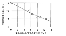
- a magnetoresistive element having no HC layer (based on Structure 2) was heated at 150 ° C. and stored for a certain period of time.
- the relationship between the average sensitivity change rate (vertical axis) and the exchange coupling bias magnitude change rate (horizontal axis) based on the value before the heat treatment at 150 ° C. was graphed. The result is shown in FIG.
- Each plot is stored from the left before heat treatment for 100 hours, 200 hours, 500 hours, 700 hours, and 1000 hours.
- FIG. 5 it was confirmed that the rate of change in the magnitude of the exchange coupling bias gradually increased and the average sensitivity rate of change decreased as the storage time at high temperature increased.
- the magnitude of the exchange coupling bias of the free magnetic layer 23 and the magnitude of the exchange coupling bias of the HC layer 25 change in the same manner as a result of high-temperature storage, and the HC layer regardless of whether or not high-temperature storage is present. It can be seen that the reflux magnetic field from 25 can appropriately reduce the hysteresis.
- the magnetoresistive effect element based on the structures 1 and 2 was heated at 150 ° C.
- the high temperature storage time dependence of the average sensitivity change rate on the basis of the value before a 150 degreeC heat processing was measured. The result is shown in FIG.
- FIG. 6 by introducing the HC layer, it is possible to reduce the sensitivity change caused by the high temperature storage of the magnetoresistive effect element.
- the magnetic sensor including the magnetoresistive effect element according to the embodiment of the present invention can be suitably used as a component of a current sensor such as a hybrid car in an electric vehicle.
Landscapes
- Physics & Mathematics (AREA)
- General Physics & Mathematics (AREA)
- Condensed Matter Physics & Semiconductors (AREA)
- Engineering & Computer Science (AREA)
- Manufacturing & Machinery (AREA)
- Hall/Mr Elements (AREA)
- Measuring Magnetic Variables (AREA)
- Measuring Instrument Details And Bridges, And Automatic Balancing Devices (AREA)
Abstract
Description
磁気センサの測定精度を向上させるためには、オフセットの低減、出力信号のばらつきの低減、およびリニアリティ(出力線形性)の向上などを実現することが求められる。これらの要求に応えるための好ましい一手段として、磁気センサが有するGMR素子のヒステリシスを低減させることが挙げられる。GMR素子のヒステリシスを低減させる手段の具体例として、フリー磁性層にバイアス磁界を印加して、被測定電流からの誘導磁界が印加されていない状態においてもフリー磁性層の磁化方向を揃えることが挙げられる。
(1)特定の方向に感度軸を持つ磁気抵抗効果素子を備えた磁気センサであって、前記磁気抵抗効果素子は、固定磁性層とフリー磁性層とが非磁性材料層を介して積層された積層構造を備え、前記フリー磁性層における前記非磁性材料層に対向する側と反対側には、前記フリー磁性層との間で交換結合バイアスを生じさせ前記フリー磁性層の磁化方向を磁化変動可能な状態で所定方向に揃えることができる反強磁性層が設けられ、前記反強磁性層における前記フリー磁性層に対向する側と反対側には、前記反強磁性層との間で交換結合バイアスが生じてその磁化方向を磁化変動可能な状態で所定方向に揃えることができる強磁性層が設けられており、前記フリー磁性層に生じた交換結合バイアスに基づく磁化方向は、前記強磁性層に生じた交換結合バイアスに基づく磁化方向と等しい向きであって、前記強磁性層は、前記フリー磁性層に対して、前記感度軸に沿った方向の成分を有する還流磁場を付与可能であることを特徴とする磁気センサ。
図1は、本発明の一実施形態に係る磁気センサの概念図(平面図)、図2は、図1に示すII-II線における矢視断面図である。
固定磁性層21は、第1磁性層21aと第2磁性層21cと、第1磁性層21aと第2磁性層21cと間に位置する非磁性中間層21bとのセルフピン止め構造である。
本発明の一実施形態に係る磁気センサの製造方法は限定されない。次に説明する方法によれば、本実施形態に係る磁気センサを効率的に製造することが可能である。
本発明の一実施形態に係る磁気抵抗効果素子を備えた磁気センサは、電流センサとして好適に使用されうる。かかる電流センサは、磁気抵抗効果素子を1つ備える構成でもよいが、特許文献1や特許文献2に記載されるように、4つの素子を用い、ブリッジ回路を組んで測定精度を高めることが好ましい。本発明の一実施形態に係る磁気抵抗効果素子の製造方法は、好ましい一例において磁場中アニール処理を備えないため、複数の磁気抵抗効果素子を同一基板上に製造することが容易である。
磁気比例式電流センサは、本発明の一実施形態に係る磁気抵抗効果素子(固定磁性層とフリー磁性層とが非磁性材料層を介して積層された積層構造を備える磁気抵抗効果素子であって、フリー磁性層における非磁性材料層に対向する側と反対側には、フリー磁性層との間で交換結合バイアスを生じさせフリー磁性層の磁化方向を磁化変動可能な状態で所定方向に揃えることができる反強磁性層が設けられ、反強磁性層におけるフリー磁性層に対向する側と反対側には、反強磁性層との間で交換結合バイアスが生じてその磁化方向を磁化変動可能な状態で所定方向に揃えることができる強磁性層が設けられており、フリー磁性層に生じた交換結合バイアスに基づく磁化方向は、強磁性層に生じた交換結合バイアスに基づく磁化方向と等しい向きであって、強磁性層は、フリー磁性層に対して、感度軸に沿った方向の成分を有する還流磁場を付与可能である、磁気抵抗効果素子。)を少なくとも1つ含んで構成され、被測定電流からの誘導磁界に応じた電圧差を生じる2つの出力を備える磁界検出ブリッジ回路を有する。そして、磁気比例式電流センサでは、誘導磁界に応じて磁界検出ブリッジ回路から出力される電位差により、被測定電流が測定される。
例えば、フリー磁性層23の磁化制御として磁場中でのアニール処理を必要としない反強磁性層24とともに従来におけるハードバイアス層を補助的に用いてもよい。
絶縁膜を有する基板上に、下からシード層20:NiFeCr(42)/固定磁性層21[第1磁性層21a;Fe60Co40(19)/非磁性中間層21b;Ru(3.6)/第2磁性層21c;Co90Fe10(24)]/非磁性材料層22;Cu(22)/フリー磁性層23[Co90Fe10(10)/Ni81Fe19(90)/Co90Fe10(10)]/反強磁性層24;Ir22Mn78(60)/HC層25[Ni81Fe19(10)/Ni82Fe13Nb5(100)]/保護層26;Ta(100)の順に積層して積層体1を得た。括弧内の数値は膜厚を示し単位はÅである。
その結果、図3に示すような結果が得られた。HC層を導入することにより、設計ストライプ幅を細くすることなく、磁気抵抗効果素子のゼロ磁場ヒステリシスを低減させることができることが確認された。
11 磁気抵抗効果素子
12 長尺パターン
21 固定磁性層
21a 第1磁性層
21b 非磁性中間層
21c 第2磁性層
22 非磁性材料層
23 フリー磁性層
24 反強磁性層
25 HC層
29 チップ
Claims (10)
- 特定の方向に感度軸を持つ磁気抵抗効果素子を備えた磁気センサであって、
前記磁気抵抗効果素子は、固定磁性層とフリー磁性層とが非磁性材料層を介して積層された積層構造を備え、
前記フリー磁性層における前記非磁性材料層に対向する側と反対側には、前記フリー磁性層との間で交換結合バイアスを生じさせ前記フリー磁性層の磁化方向を磁化変動可能な状態で所定方向に揃えることができる反強磁性層が設けられ、
前記反強磁性層における前記フリー磁性層に対向する側と反対側には、前記反強磁性層との間で交換結合バイアスが生じてその磁化方向を磁化変動可能な状態で所定方向に揃えることができる強磁性層が設けられており、
前記フリー磁性層に生じた交換結合バイアスに基づく磁化方向は、前記強磁性層に生じた交換結合バイアスに基づく磁化方向と等しい向きであって、
前記強磁性層は、前記フリー磁性層に対して、前記感度軸に沿った方向の成分を有する還流磁場を付与可能であること
を特徴とする磁気センサ。 - 前記強磁性層に生じた交換結合バイアスの大きさおよび前記強磁性層の厚さは、前記フリー磁性層の残留磁化の前記感度軸に沿った方向の成分を低減させるように設定される、請求項1に記載の磁気センサ。
- 前記反強磁性層は、IrMnにより形成される、請求項1または2に記載の磁気センサ。
- 前記固定磁性層は、第1磁性層と前記非磁性材料層に接する第2磁性層とが非磁性中間層を介して積層され、前記第1磁性層と前記第2磁性層とが反平行に磁化固定されたセルフピン止め型である、請求項1から3のいずれか一項に記載の磁気センサ。
- 前記強磁性層に生じた交換結合バイアスの大きさおよび前記強磁性層の厚さは、前記フリー磁性層の感度の高温保存時間依存性を低減させるように設定される、請求項1から4のいずれか一項に記載の磁気センサ。
- 基板上に、シード層、固定磁性層、非磁性材料層、フリー磁性層、反強磁性層および強磁性層をこの順に積層する工程を備える磁気センサの製造方法であって、
積層方向に直交する第1の方向に磁場を印加しながら第1磁性層を前記シード層上に積層し、続いて非磁性中間層および第2磁性層を順次積層することにより、セルフピン止め構造を備える積層体からなる前記固定磁性層を得るピン層積層工程;
前記第2磁性層上に非磁性材料層を積層する非磁性層積層工程;および
前記第1の方向とは異なる方向である第2の磁場を印加しながら、前記非磁性材料層上に、前記フリー磁性層、前記反強磁性層および前記強磁性層を順次積層するフリー層積層工程を備えること
を特徴とする磁気センサの製造方法。 - 前記強磁性層から前記フリー磁性層に対して、前記第1の方向に平行な方向への還流磁場が印加可能に、前記強磁性層の構造は設定される、請求項6に記載の磁気センサの製造方法。
- 前記シード層を積層する工程から、前記強磁性層を積層する工程まで、磁場中アニール処理が行われない、請求項6または7に記載の磁気センサの製造方法。
- 前記反強磁性層を、IrMnにより形成する請求項8に記載の磁気センサの製造方法。
- 請求項1から5のいずれか一項に記載される磁気センサを備える電流センサ。
Priority Applications (4)
| Application Number | Priority Date | Filing Date | Title |
|---|---|---|---|
| JP2016510218A JP6233863B2 (ja) | 2014-03-28 | 2015-03-11 | 磁気センサおよび磁気センサの製造方法ならびに電流センサ |
| EP15768683.3A EP3125319B1 (en) | 2014-03-28 | 2015-03-11 | Magnetic sensor, method for manufacturing magnetic sensor, and current sensor |
| CN201580014136.0A CN106133934B (zh) | 2014-03-28 | 2015-03-11 | 磁传感器及磁传感器的制造方法以及电流传感器 |
| US15/237,846 US9945913B2 (en) | 2014-03-28 | 2016-08-16 | Magnetic sensor, method for manufacturing magnetic sensor, and current sensor |
Applications Claiming Priority (2)
| Application Number | Priority Date | Filing Date | Title |
|---|---|---|---|
| JP2014-069478 | 2014-03-28 | ||
| JP2014069478 | 2014-03-28 |
Related Child Applications (1)
| Application Number | Title | Priority Date | Filing Date |
|---|---|---|---|
| US15/237,846 Continuation US9945913B2 (en) | 2014-03-28 | 2016-08-16 | Magnetic sensor, method for manufacturing magnetic sensor, and current sensor |
Publications (1)
| Publication Number | Publication Date |
|---|---|
| WO2015146593A1 true WO2015146593A1 (ja) | 2015-10-01 |
Family
ID=54195117
Family Applications (1)
| Application Number | Title | Priority Date | Filing Date |
|---|---|---|---|
| PCT/JP2015/057200 WO2015146593A1 (ja) | 2014-03-28 | 2015-03-11 | 磁気センサおよび磁気センサの製造方法ならびに電流センサ |
Country Status (5)
| Country | Link |
|---|---|
| US (1) | US9945913B2 (ja) |
| EP (1) | EP3125319B1 (ja) |
| JP (1) | JP6233863B2 (ja) |
| CN (1) | CN106133934B (ja) |
| WO (1) | WO2015146593A1 (ja) |
Cited By (4)
| Publication number | Priority date | Publication date | Assignee | Title |
|---|---|---|---|---|
| CN106872914A (zh) * | 2015-11-27 | 2017-06-20 | 爱盛科技股份有限公司 | 磁场感测装置及感测方法 |
| US20170371006A1 (en) * | 2016-06-23 | 2017-12-28 | Alps Electric Co., Ltd. | Magnetic sensor and current sensor |
| TWI613458B (zh) * | 2015-11-27 | 2018-02-01 | 愛盛科技股份有限公司 | 磁場感測裝置及其感測方法 |
| WO2018037634A1 (ja) * | 2016-08-23 | 2018-03-01 | アルプス電気株式会社 | 磁気センサおよび電流センサ |
Families Citing this family (7)
| Publication number | Priority date | Publication date | Assignee | Title |
|---|---|---|---|---|
| CN111615636B (zh) * | 2018-01-17 | 2022-07-08 | 阿尔卑斯阿尔派株式会社 | 磁检测装置及其制造方法 |
| JP6610746B1 (ja) * | 2018-10-24 | 2019-11-27 | Tdk株式会社 | 磁気センサ |
| WO2020137558A1 (ja) * | 2018-12-27 | 2020-07-02 | アルプスアルパイン株式会社 | 交換結合膜ならびにこれを用いた磁気抵抗効果素子および磁気検出装置 |
| US11131727B2 (en) * | 2019-03-11 | 2021-09-28 | Tdk Corporation | Magnetic sensor device |
| JP6984792B2 (ja) * | 2019-06-11 | 2021-12-22 | 株式会社村田製作所 | 磁気センサ、磁気センサアレイ、磁場分布測定装置、および位置特定装置 |
| CN110444531B (zh) * | 2019-08-23 | 2021-05-25 | 上海华虹宏力半导体制造有限公司 | 3d磁传感器的漏电流测试结构及其形成方法 |
| US11719772B2 (en) | 2020-04-01 | 2023-08-08 | Analog Devices International Unlimited Company | AMR (XMR) sensor with increased linear range |
Citations (4)
| Publication number | Priority date | Publication date | Assignee | Title |
|---|---|---|---|---|
| JP2001357505A (ja) * | 2000-06-13 | 2001-12-26 | Sony Corp | 磁気抵抗効果素子、磁気ヘッド及び再生装置 |
| JP2003536267A (ja) * | 2000-06-21 | 2003-12-02 | コーニンクレッカ フィリップス エレクトロニクス エヌ ヴィ | 改善された磁場範囲を有する磁気多層構造 |
| JP2004206839A (ja) * | 2002-12-26 | 2004-07-22 | Tdk Corp | 薄膜磁気ヘッド、薄膜磁気ヘッド組立体、記憶装置、及び薄膜磁気ヘッドの製造方法 |
| WO2012081377A1 (ja) * | 2010-12-16 | 2012-06-21 | アルプス電気株式会社 | 磁気センサ及び磁気センサの製造方法 |
Family Cites Families (4)
| Publication number | Priority date | Publication date | Assignee | Title |
|---|---|---|---|---|
| JP3908557B2 (ja) * | 2001-10-09 | 2007-04-25 | アルプス電気株式会社 | 磁気検出素子の製造方法 |
| US7573734B2 (en) * | 2007-07-13 | 2009-08-11 | Consejo Superior De Investigaciones Cientificas | Magnetoelectric device and method for writing non-volatile information into said magnetoelectric device |
| DE102007032867B4 (de) * | 2007-07-13 | 2009-12-24 | Infineon Technologies Ag | Magnetoresistive Magnetfeldsensorstrukturen und Herstellungsverfahren |
| JP5686635B2 (ja) * | 2011-03-07 | 2015-03-18 | アルプス電気株式会社 | 磁気センサ及びその製造方法 |
-
2015
- 2015-03-11 CN CN201580014136.0A patent/CN106133934B/zh active Active
- 2015-03-11 WO PCT/JP2015/057200 patent/WO2015146593A1/ja active Application Filing
- 2015-03-11 JP JP2016510218A patent/JP6233863B2/ja active Active
- 2015-03-11 EP EP15768683.3A patent/EP3125319B1/en active Active
-
2016
- 2016-08-16 US US15/237,846 patent/US9945913B2/en active Active
Patent Citations (4)
| Publication number | Priority date | Publication date | Assignee | Title |
|---|---|---|---|---|
| JP2001357505A (ja) * | 2000-06-13 | 2001-12-26 | Sony Corp | 磁気抵抗効果素子、磁気ヘッド及び再生装置 |
| JP2003536267A (ja) * | 2000-06-21 | 2003-12-02 | コーニンクレッカ フィリップス エレクトロニクス エヌ ヴィ | 改善された磁場範囲を有する磁気多層構造 |
| JP2004206839A (ja) * | 2002-12-26 | 2004-07-22 | Tdk Corp | 薄膜磁気ヘッド、薄膜磁気ヘッド組立体、記憶装置、及び薄膜磁気ヘッドの製造方法 |
| WO2012081377A1 (ja) * | 2010-12-16 | 2012-06-21 | アルプス電気株式会社 | 磁気センサ及び磁気センサの製造方法 |
Non-Patent Citations (1)
| Title |
|---|
| See also references of EP3125319A4 * |
Cited By (7)
| Publication number | Priority date | Publication date | Assignee | Title |
|---|---|---|---|---|
| CN106872914A (zh) * | 2015-11-27 | 2017-06-20 | 爱盛科技股份有限公司 | 磁场感测装置及感测方法 |
| TWI613458B (zh) * | 2015-11-27 | 2018-02-01 | 愛盛科技股份有限公司 | 磁場感測裝置及其感測方法 |
| US10151807B2 (en) | 2015-11-27 | 2018-12-11 | Isentek Inc. | Magnetic field sensing apparatus with anisotropic magneto-resistive resistors and detection method thereof |
| CN106872914B (zh) * | 2015-11-27 | 2019-09-10 | 爱盛科技股份有限公司 | 磁场感测装置及感测方法 |
| US20170371006A1 (en) * | 2016-06-23 | 2017-12-28 | Alps Electric Co., Ltd. | Magnetic sensor and current sensor |
| WO2018037634A1 (ja) * | 2016-08-23 | 2018-03-01 | アルプス電気株式会社 | 磁気センサおよび電流センサ |
| JPWO2018037634A1 (ja) * | 2016-08-23 | 2019-04-11 | アルプスアルパイン株式会社 | 磁気センサおよび電流センサ |
Also Published As
| Publication number | Publication date |
|---|---|
| JP6233863B2 (ja) | 2017-11-22 |
| US9945913B2 (en) | 2018-04-17 |
| EP3125319A4 (en) | 2017-12-13 |
| EP3125319B1 (en) | 2018-09-12 |
| JPWO2015146593A1 (ja) | 2017-04-13 |
| CN106133934B (zh) | 2018-11-02 |
| US20160356865A1 (en) | 2016-12-08 |
| CN106133934A (zh) | 2016-11-16 |
| EP3125319A1 (en) | 2017-02-01 |
Similar Documents
| Publication | Publication Date | Title |
|---|---|---|
| JP6233863B2 (ja) | 磁気センサおよび磁気センサの製造方法ならびに電流センサ | |
| US8952689B2 (en) | Magnetic sensor and magnetic balance type current sensor utilizing same | |
| US20110221436A1 (en) | Current sensor | |
| US20130257422A1 (en) | Magnetic sensor and method for manufacturing magnetic sensor | |
| WO2012090631A1 (ja) | 磁気比例式電流センサ | |
| US20170371006A1 (en) | Magnetic sensor and current sensor | |
| JP2012119613A (ja) | 磁気検出素子及びそれを用いた磁気センサ | |
| JP5447616B2 (ja) | 磁気センサの製造方法 | |
| JP6776120B2 (ja) | 磁気検出装置、磁気検出装置の製造方法および磁気検出装置を用いてなる電流検出装置 | |
| JP6755319B2 (ja) | 磁気センサおよび電流センサ | |
| JP2011027633A (ja) | 磁気センサおよびその製造方法 | |
| JP6282990B2 (ja) | 磁気センサおよび電流センサ | |
| EP2953178B1 (en) | Giant magnetoresistive element and current sensor using same | |
| JP5540326B2 (ja) | 電流センサ | |
| EP3059601B1 (en) | Magnetometric sensor and current sensor | |
| JP2017040509A (ja) | 磁気センサおよび電流センサ | |
| JP6204391B2 (ja) | 磁気センサおよび電流センサ | |
| JP7261656B2 (ja) | 磁気センサおよびその製造方法 | |
| JP2017139269A (ja) | 磁気センサ、磁気センサの製造方法および電流センサ | |
| JP6713867B2 (ja) | デュアルスピンバルブ磁気検出素子の製造方法およびデュアルスピンバルブ磁気検出素子を使用した磁気検出装置の製造方法 | |
| JP5517315B2 (ja) | 電流センサ | |
| JP2020136306A (ja) | 交換結合膜、磁気抵抗効果素子および磁気検出装置 |
Legal Events
| Date | Code | Title | Description |
|---|---|---|---|
| 121 | Ep: the epo has been informed by wipo that ep was designated in this application |
Ref document number: 15768683 Country of ref document: EP Kind code of ref document: A1 |
|
| ENP | Entry into the national phase |
Ref document number: 2016510218 Country of ref document: JP Kind code of ref document: A |
|
| REEP | Request for entry into the european phase |
Ref document number: 2015768683 Country of ref document: EP |
|
| WWE | Wipo information: entry into national phase |
Ref document number: 2015768683 Country of ref document: EP |
|
| NENP | Non-entry into the national phase |
Ref country code: DE |