WO2015137364A1 - プラズマ処理装置 - Google Patents
プラズマ処理装置 Download PDFInfo
- Publication number
- WO2015137364A1 WO2015137364A1 PCT/JP2015/057067 JP2015057067W WO2015137364A1 WO 2015137364 A1 WO2015137364 A1 WO 2015137364A1 JP 2015057067 W JP2015057067 W JP 2015057067W WO 2015137364 A1 WO2015137364 A1 WO 2015137364A1
- Authority
- WO
- WIPO (PCT)
- Prior art keywords
- wafer
- plasma processing
- plasma
- processing chamber
- unit
- Prior art date
- Legal status (The legal status is an assumption and is not a legal conclusion. Google has not performed a legal analysis and makes no representation as to the accuracy of the status listed.)
- Ceased
Links
Images








Classifications
-
- H—ELECTRICITY
- H10—SEMICONDUCTOR DEVICES; ELECTRIC SOLID-STATE DEVICES NOT OTHERWISE PROVIDED FOR
- H10P—GENERIC PROCESSES OR APPARATUS FOR THE MANUFACTURE OR TREATMENT OF DEVICES COVERED BY CLASS H10
- H10P72/00—Handling or holding of wafers, substrates or devices during manufacture or treatment thereof
- H10P72/04—Apparatus for manufacture or treatment
- H10P72/0402—Apparatus for fluid treatment
- H10P72/0418—Apparatus for fluid treatment for etching
- H10P72/0421—Apparatus for fluid treatment for etching for drying etching
-
- H—ELECTRICITY
- H10—SEMICONDUCTOR DEVICES; ELECTRIC SOLID-STATE DEVICES NOT OTHERWISE PROVIDED FOR
- H10P—GENERIC PROCESSES OR APPARATUS FOR THE MANUFACTURE OR TREATMENT OF DEVICES COVERED BY CLASS H10
- H10P50/00—Etching of wafers, substrates or parts of devices
- H10P50/20—Dry etching; Plasma etching; Reactive-ion etching
- H10P50/24—Dry etching; Plasma etching; Reactive-ion etching of semiconductor materials
- H10P50/242—Dry etching; Plasma etching; Reactive-ion etching of semiconductor materials of Group IV materials
-
- H—ELECTRICITY
- H01—ELECTRIC ELEMENTS
- H01J—ELECTRIC DISCHARGE TUBES OR DISCHARGE LAMPS
- H01J37/00—Discharge tubes with provision for introducing objects or material to be exposed to the discharge, e.g. for the purpose of examination or processing thereof
- H01J37/32—Gas-filled discharge tubes
- H01J37/32009—Arrangements for generation of plasma specially adapted for examination or treatment of objects, e.g. plasma sources
- H01J37/32082—Radio frequency generated discharge
-
- H—ELECTRICITY
- H01—ELECTRIC ELEMENTS
- H01J—ELECTRIC DISCHARGE TUBES OR DISCHARGE LAMPS
- H01J37/00—Discharge tubes with provision for introducing objects or material to be exposed to the discharge, e.g. for the purpose of examination or processing thereof
- H01J37/32—Gas-filled discharge tubes
- H01J37/32009—Arrangements for generation of plasma specially adapted for examination or treatment of objects, e.g. plasma sources
- H01J37/32192—Microwave generated discharge
-
- H—ELECTRICITY
- H01—ELECTRIC ELEMENTS
- H01J—ELECTRIC DISCHARGE TUBES OR DISCHARGE LAMPS
- H01J37/00—Discharge tubes with provision for introducing objects or material to be exposed to the discharge, e.g. for the purpose of examination or processing thereof
- H01J37/32—Gas-filled discharge tubes
- H01J37/32431—Constructional details of the reactor
- H01J37/32715—Workpiece holder
-
- H—ELECTRICITY
- H10—SEMICONDUCTOR DEVICES; ELECTRIC SOLID-STATE DEVICES NOT OTHERWISE PROVIDED FOR
- H10P—GENERIC PROCESSES OR APPARATUS FOR THE MANUFACTURE OR TREATMENT OF DEVICES COVERED BY CLASS H10
- H10P72/00—Handling or holding of wafers, substrates or devices during manufacture or treatment thereof
- H10P72/04—Apparatus for manufacture or treatment
- H10P72/0451—Apparatus for manufacturing or treating in a plurality of work-stations
- H10P72/0462—Apparatus for manufacturing or treating in a plurality of work-stations characterised by the construction of the processing chambers, e.g. modular processing chambers
-
- H—ELECTRICITY
- H01—ELECTRIC ELEMENTS
- H01J—ELECTRIC DISCHARGE TUBES OR DISCHARGE LAMPS
- H01J2237/00—Discharge tubes exposing object to beam, e.g. for analysis treatment, etching, imaging
- H01J2237/32—Processing objects by plasma generation
- H01J2237/33—Processing objects by plasma generation characterised by the type of processing
- H01J2237/334—Etching
Definitions
- the present invention relates to a processing apparatus suitable for a minimal fab system for manufacturing semiconductor devices and the like, and more particularly to a processing apparatus useful for plasma processing.
- the current semiconductor manufacturing system is 3000 to 500 billion yen to start up the latest semiconductor factory (megafab production system) as the equipment itself becomes larger and more expensive as wafer diameter increases (from 12 inches) It is said that huge investment funds are required.
- a system using a large-diameter wafer is efficient for mass production.
- the device is operated for high-mix low-volume production, the number of pieces required by the user is limited due to problems such as availability. The manufacturing cost will be very high.
- the manufacturing system is configured based on the production of one device on a wafer of 0.5 inch size (half inch size, more precisely, 12.5 mm in diameter).
- each processing step is a portable processing device and making it easy to relocate these processing devices to a flow shop, job shop, etc. according to the recipe, it is possible to produce in small quantities and multi-product production
- a minimal fab system has been proposed by the present applicant to enable an appropriate response.
- Patent Document 1 This minimal fab system is expected to require an extremely small capital investment of about 1/1000 compared to the current semiconductor manufacturing system, and is suitable for high-mix low-volume production due to low operating costs. It is expected to become a production system.
- Each of the processing apparatuses used in this minimal fab system bears one of individual processes in the process of the semiconductor manufacturing apparatus (in Patent Document 1, this is defined as “single process”).
- they are a wafer cleaning apparatus, a resist coating apparatus, a wafer exposure apparatus, a plasma processing apparatus, and an ion implantation apparatus.
- a coating apparatus, an exposure apparatus, a plasma generation apparatus, and the like necessary for the processing, as well as a power supply apparatus and a control apparatus necessary for driving them are incorporated together.
- These processing apparatuses are arranged in the order of recipes for semiconductor manufacturing (processing flow order). Wafers, which are workpieces, are sequentially conveyed between the arranged processing apparatuses, and the corresponding processing is sequentially performed in each processing apparatus.
- this processing apparatus can be rearranged freely in accordance with the recipe each time the recipe is changed, and in addition, when the arrangement is changed, the processing apparatus is set in a predetermined position on the work floor in advance. It is a portable and uniform predetermined size that can be carried by people so that it can be connected to regularly arranged juxtaposed supply systems, drainage systems, power supply systems, and the like. According to the processing apparatus described in Patent Document 1, the size of this processing apparatus is an external dimension of width 0.30 m ⁇ depth 0.45 m ⁇ height 1.44 m, which is not only extremely small per se. Even if 60 are arranged according to the semiconductor manufacturing recipe, the occupied floor area is considered to be extremely small compared to the existing 12-inch semiconductor manufacturing apparatus.
- the wafer which is a workpiece
- the wafer is a production system in which the wafer is transferred between the processing apparatuses by a unique hermetic transfer system that is substantially cut off from the outside air. . Therefore, it is sufficient that only a predetermined processing space in each processing apparatus is a necessary processing atmosphere, for example, a clean room space or a vacuum state space, and it is necessary to arrange the processing apparatus itself in the clean room. No. This is fundamentally different from the existing semiconductor manufacturing system in which the semiconductor processing apparatus itself is arranged in a huge clean room. Therefore, in this minimal fab system, since it is not necessary to arrange the processing apparatus in the clean room, the worker can work in a normal working environment without being forced to work in the clean room. It also saves energy because there is no need to create a huge clean room space. As described above, the minimal fab system is attracting attention as an innovative next-generation production system, not a production system in which a conventional apparatus is simply reduced in size.
- Patent Document 2 What is cooled by the above is known (Patent Document 2).
- the size of the apparatus itself does not matter so much as an apparatus for a large-diameter wafer, but in order to make this a processing apparatus incorporated in the above-mentioned minimal fab system, The plasma generator and the power supply for it are too large.
- the processing apparatus incorporated in the minimal fab system has not only a storage space for the entire apparatus, but also a processing space for performing various processes in the apparatus, so various functions must be incorporated in such a narrow space.
- a plasma processing apparatus taking a plasma processing apparatus as an example, an airtight chamber for receiving a semiconductor wafer is installed in a very narrow space compared to a conventional plasma processing apparatus, and plasma is generated by supporting the semiconductor wafer in the airtight chamber and is stable. It must be controlled so that the plasma etching can be performed.
- a power supply device, a control device, a gas supply device, and the like for that purpose must also be incorporated into the processing apparatus.
- it must have a transfer function for reliably transferring and holding a small half-inch wafer at a predetermined processing position in the processing space. And a uniform process must be performed over the entire wafer surface.
- microplasma (1) the generation of plasma is isotropic, and therefore isotropic etching, (2) it is not as hot as other thermal plasmas, Because of the accompanying plasma, so-called “resist burning” often occurs, and (3) “fluctuation” of the concentration occurs in the plasma that is formed, as described by a lighter flame. (4) Since the generated plasma is a small reaction field, only spot irradiation can be performed, and even when a half-inch wafer is targeted, the entire wafer is irradiated uniformly.
- the present invention provides a wafer support device for supporting a wafer to be processed, a wafer holding portion provided on an upper portion of the wafer support device, and the wafer holding portion, which is substantially free from outside air. And a wafer processing unit provided in the processing chamber, wherein the wafer support device includes the wafer holding unit and the wafer holding unit.
- a shaft portion that supports and extends outside the processing chamber, a drive portion that is connected to the shaft portion outside the processing chamber and moves the shaft portion in the XYZ axial directions, and processing by the wafer processing portion is uniform over the entire wafer surface.
- a control device for controlling the drive unit so that the wafer held by the wafer holding unit is moved by the operation of the drive unit with respect to the wafer processing unit in the processing chamber. That it is relatively movable over a for minimal fab system processing apparatus according to claim.
- the plasma power supply device may have a small output capable of generating microplasma, so that it can be a small power supply device and is extremely space-saving. Can be. Further, by superimposing RF on the generated microplasma, the isotropy of the microplasma can be improved, so that the etch rate can be improved.
- the processing surface of the workpiece is made uniform. Plasma treatment can be performed. Also, by moving the workpiece within the processing plane, even if it is spot irradiation, even etching processing can be performed, and even if such scanning is performed, the processing area of the workpiece itself is small, so the processing time There is no particular need to consider. It is impossible to realize such uniform processing efficiently in a short time with a megafab system using a large-diameter wafer. Scanning here is different from scanning in a processing apparatus for patterning a figure such as an exposure apparatus.
- the purpose is to process a non-uniform structure on the workpiece, so it is necessary to perform extremely fine scanning control.
- scanning in the present invention is not performed in such scanning for patterning. Rather, it is performed for the purpose of uniformly performing processing by the processing apparatus within the processing surface of the workpiece, and for example, the processing apparatus is moved in the XY-axis direction so as to draw a Lissajous figure.
- the structure is space-saving and efficient cooling can be performed. This can also prevent resist burning.
- a processing apparatus suitable for incorporation into a minimal fab system can reliably support a workpiece from outside the processing space, has excellent cooling efficiency, and is uniform over the entire wafer surface. Therefore, it is possible to provide a processing apparatus that is compactly configured with functions that enable easy processing.
- a plasma processing apparatus suitable for incorporation into a minimal fab system can be provided.
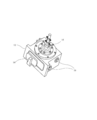
- FIG. 1 is a conceptual diagram of a plasma processing apparatus M.
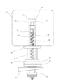
- FIG. 2 is a side view of a main part of a plasma processing apparatus M.
- FIG. 3 is a perspective view of main parts of a wafer support device 19.
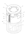
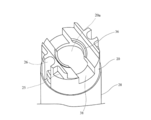
- FIG. 3 is a perspective view of a wafer cradle 20.
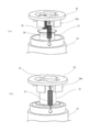
- FIG. 6 is an exploded perspective view of main parts showing the operation of the wafer support device 19. It is a perspective view of a drive mechanism.
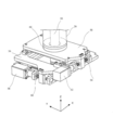
- A) is a perspective view which shows the bottom face of the plasma processing chamber 12, and the state of the downward direction
- (b) is a principal part longitudinal cross-sectional view.
- FIG. 5 is a longitudinal sectional view of the periphery of the wafer support 22 in another example (2) according to the present embodiment.
- Explanatory drawing which shows the effectiveness of the plasma processing apparatus of this invention.
- A is a figure explaining the effectiveness of superimposing RF on microplasma
- (b) is a figure explaining that the uniformity of the in-plane etch rate improved with scanning of a wafer.
- FIGS. 6A and 6B are diagrams illustrating wafer scanning conditions by the plasma processing apparatus according to the first to sixth embodiments, in which FIG. 5A is a distance R movement from an initial position, and FIG.
- the plasma processing apparatus M includes a main body Ma that stores the plasma processing chamber 12 and a control storage Mb that stores a power supply device, a control device, a gas supply device, and the like.
- the front part of the plasma processing apparatus M is provided with a front chamber Mc for transferring the wafer to the plasma processing chamber in the main body Ma.
- the front chamber Mc is configured to have a transfer function and an outer shape that are common to all other processing apparatuses of the minimal fab system.
- a support portion m is provided below the plasma processing apparatus M for positioning and holding the plasma processing apparatus M at a predetermined position on the floor.
- Semiconductor wafers (workpieces) 18 to be processed by the plasma processing apparatus M are stored one by one in a wafer storage shuttle (not shown) and transferred to the plasma processing apparatus M.
- the shuttle is configured so that one semiconductor wafer having a diameter of 0.5 inch (half inch size, to be precise, 12.5 mm) is accommodated while being substantially shielded from the outside air.
- a docking port 82 for connecting the front room Mc and the shuttle is provided in the upper part of the front room Mc.
- a wafer transfer space connected to the docking port 82 is provided inside the front chamber Mc, and the wafer transfer space is configured to be in a high vacuum state by a high vacuum pump.
- An airtight gate valve 14 is provided between the wafer transfer space and the plasma processing chamber 12 (FIG. 2). Further, in the wafer transfer space, the wafer 18 in the shuttle on the docking port 82 is taken out in a state of being blocked from the outside air, and the taken-out wafer 18 is passed through the gate valve 14 opened to pass through the plasma processing chamber 12.
- a transfer mechanism (not shown) for transferring the wafer to the wafer support device 19 is provided.
- a display-type operation panel 81 is provided above the front chamber Mc.
- this minimal fab system includes a closed-type transport mechanism (Particle-Lock AirtightkingDocking: PLAD) that substantially shuts off fine particles and gas molecules from the outside world, including a shuttle and a transport mechanism provided in the front chamber Mc. System).
- the semiconductor wafer 18 as a target is loaded into the front chamber Mc from another processing apparatus via the shuttle by the PLAD system, and is transferred into the plasma processing chamber 12 by a transfer mechanism (not shown) in the front chamber Mc. It is carried onto a wafer support device (work support device) 19. Then, the semiconductor wafer 18 that has been plasma-etched on the wafer support device is carried out (returned) into the shuttle on the docking port 82 by the PLAD system.
- the semiconductor wafer 18 that has been plasma-treated in this way is stored in the shuttle and is transported to the next processing apparatus according to the recipe.
- the appearance of the plasma processing chamber is shown in FIG.
- the plasma processing chamber 12 is provided with a gate valve 14 for taking the semiconductor wafer 18 in and out of the front chamber Mc.
- the gate valve 14 serves as a wafer entrance / exit that communicates with the front chamber Mc, and is configured so that the inside of the plasma processing chamber 12 can be maintained at a predetermined degree of vacuum.
- the plasma processing chamber 12 is provided with a gas supply port 15 for supplying an active gas such as CF 4 and a gas discharge port 16 therein. These are mechanisms for supplying and exhausting an etching gas.
- a supply mechanism such as a gas supply source is also accommodated in the space inside the plasma processing apparatus M shown in FIG.
- a plasma generation mechanism in the plasma processing chamber 12 will be described with reference to FIG.
- cylindrical electrodes are provided at intervals of several millimeters in a CF 4 / Ar gas supply pipe, and a predetermined high voltage is applied between them. Is arranged. In the present embodiment, the applied voltage was 8 KHz, peak value 7 kV, and output 20 W.
- Microplasma generated by the microplasma generator Mo is supplied into the plasma processing chamber 12.
- an RF plasma apparatus Mr for superimposing RF on the supplied microplasma is disposed.
- the RF plasma apparatus Mr is configured such that a lower electrode 35 is provided on a wafer support 22 on which a wafer 18 is placed, and an alternating current is applied to the lower electrode 35.
- the applied high frequency is 13.56 MHz, 25 to 50 W, and the degree of vacuum is 100 Pascals.
- the plasma processing apparatus M in the present embodiment is configured such that after microplasma is generated, RF can be further superimposed on the microplasma. With this configuration, a microplasma jet P with a reduced plasma characteristic length is generated inside the plasma processing chamber 12.
- the wafer support 22 is parallel to the processing surface of the semiconductor wafer 18 placed thereon (that is, in the X direction shown in FIG. 1). It is configured to perform scanning movement in a direction parallel to the support table 22. A configuration for performing the scanning movement will be described later.
- the horizontal axis represents the wafer position and the vertical axis represents the etching rate, and the above-described RF superposition effect and the scan effect of the wafer support 22 were investigated. Since the wafer diameter is 12.5 mm, a radius of 6.25 mm becomes the wafer edge. The wafer is fixed by a clamp 24, and there is a holding allowance for the clamp 24 with a width of 0.5 mm from the outermost periphery. Therefore, data plots were made every 5 mm from the center to 5 mm.
- the stage scan (XY scanning) effect As shown in FIG. 12B, regarding the stage scan (XY scanning) effect, the in-plane etch rate distribution in the case where the stage scan is not performed has a Gaussian distribution shape. The non-uniformity was improved to 3.5%. Therefore, it can be seen that the stage scan had a dramatic effect.
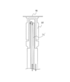
- FIG. 3 is a side view of the main part including the plasma processing chamber 12.
- the alternate long and short dash line in the figure indicates the position of the outer wall surface of the plasma processing chamber 12.
- An external view of the plasma processing chamber 12 is not shown.
- the lower side of the plasma processing chamber 12 is a schematic side view.
- the upper end of the wafer support device 19 protrudes into the plasma processing chamber 12 so as to penetrate the bottom plate.
- the wafer support device 19 is provided at its upper end with a wafer holder for holding the semiconductor wafer 18, and below the wafer holder is a shaft extending outside the plasma processing chamber 12.
- the wafer holding part is composed of a wafer cradle 20, a wafer support pedestal 22, and a wafer presser plate 24.
- the wafer cradle 20 is fixed to the upper end of a protective tube 28 that forms the outermost part of the shaft part. And is supported at a predetermined position in the processing chamber.
- a cylindrical through-hole 20 a penetrating in the vertical direction is provided at the center of the wafer cradle 20.
- a wafer support 22 that moves up and down relative to the wafer cradle 20 is provided in the through-hole 20 a. Is provided.
- the upper surface of the wafer support 22 is a mounting surface on which the semiconductor wafer 18 is placed at the processing position.
- the wafer support 22 and a wafer pressing plate 24 provided above the wafer support 22 are provided.
- the semiconductor wafer (work) 18 (not shown in FIG. 3) is sandwiched and supported.
- the wafer gripping mechanism including the wafer cradle 20, the wafer support 22 and the wafer pressing plate 24 will be described in detail later.
- a protective tube 28 is provided below the wafer pedestal 20 so as to be continuous with the wafer pedestal 20.
- a refrigerant supply tube 30, a cooling tube 32, and a power feeding body 34 are provided inside the protective tube 28 .
- a lower electrode 35 (not shown in FIG. 3) is provided inside the protective tube 28 .
- the refrigerant supply pipe 30 is provided so as to cover the cooling pipe 32 and is configured to supply the refrigerant to the cooling pipe 32.
- the power feeding body 34 is provided so as to feed power to the lower electrode 35, and the cooling pipe 32 is wound around the power feeding body 34 to cool the power feeding body 34 and the lower electrode 35 and is supplied to the refrigerant supply pipe 30. It is comprised so that the refrigerant
- the protective tube 28 that supports the wafer pedestal 20, the coolant supply tube 30 that supports the wafer support 22, the cooling tube 32, etc. are all formed of stainless steel pipes or the like.
- the wafer support 22 is preferably made of a material having a high cooling effect on the semiconductor wafer 18 to be placed, such as ceramic.
- FIG. 3 only the outline of the wafer pressing plate 24, the wafer cradle 20, and the protective tube 28 is indicated by a one-dot chain line. Only the outline of the refrigerant supply pipe 30 is shown by a solid line. Further, the inside of the protective tube 28 is shown by a broken line, and the lower portion is not shown.
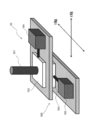
- FIG. 4 is a perspective view of the main part of the wafer support device 19.
- FIG. 5 is a perspective view of the wafer cradle 20.
- FIG. 6 is an exploded perspective view of the main part showing the operation of the wafer support device 19.
- a wafer gripping mechanism by a wafer holding part provided at the upper end part of the wafer support apparatus will be described with reference to FIGS.
- a wafer holding unit that is, a wafer receiving table 20, a wafer supporting table 22, and a wafer pressing plate 24 are provided at the upper end of the wafer supporting device 19.
- the wafer cradle 20 is fixed to the upper end of the protective tube 28 and supported at a predetermined position in the processing chamber, as shown in FIG.
- a cylindrical through-hole 20a is provided at the center, and a wafer holding groove (wafer mounting portion) 36 into which a half-inch semiconductor wafer 18 is fitted is substantially formed at the upper end of the through-hole 20a. It is provided in a half moon shape. Furthermore, an arm groove 38 extending to the side surface of the wafer pedestal 20 is formed deeper below the wafer holding groove 36 in the wafer pedestal 20 so as to cross the through hole 20a.
- the shaft portion of the wafer support base 22 is inserted into the through hole 20a of the wafer base 20, and the upper end surface of the wafer support base 22 is located above and below the wafer holding groove 36. It is possible to move in the vertical direction with respect to the wafer cradle 20 so that the wafer can be positioned at the same position. Further, a guide groove 25 for guiding the leg portion 24a of the wafer retainer plate 24 and a spring 26a for applying a tensile force to the wafer retainer plate 24 and the wafer retainer 20 are housed on the side surface of the wafer retainer 20 in the vertical direction. A spring groove 26 is provided.
- the wafer pressing plate 24 is configured to slide in the direction in which the wafer support base 22 moves up and down along the guide groove 25 of the wafer receiving base 20.
- the wafer pressing plate 24 is connected to the upper end of the protective tube 28 by a spring 26a.
- the wafer pressing plate 24 presses the peripheral portion of the semiconductor wafer 18 in the direction of the wafer support 22 by the elasticity of the spring 26a.
- the semiconductor wafer 18 conveyed by an arm (which constitutes a part of the PLAD system described above, not shown) extending from the front chamber Mc is fitted.
- the arm groove 38 is for allowing the arm to pass therethrough.
- the tip of the arm extending from the front chamber Mc through the gate valve 14 enters the arm groove 38 and enters the wafer holding groove 36 without colliding with the wafer cradle 20.
- the semiconductor wafer 18 can be accessed (or the tip of the arm can carry the semiconductor wafer 18 held at the tip of the arm into the wafer holding groove 36 without colliding with the wafer cradle 20, and then , You can safely return to the front chamber Mc.)
- the wafer pressing plate 24 and the wafer cradle 20 are both formed of a ceramic molded product, for example.
- FIG. 6 is an exploded perspective view of the main part showing the operation of the wafer support device 19.
- This figure shows a state in which the wafer cradle 20 is removed, (a) is a state immediately after receiving the semiconductor wafer 18, and (b) is a state in which the semiconductor wafer 18 is lifted by the wafer support 22 and pressed against the wafer pressing plate 24. The state is shown. In the state (b), it can be clearly seen that the spring 26 a is slightly extended and the semiconductor wafer 18 is sandwiched between the wafer support 22 and the wafer pressing plate 24. An RF plasma (microplasma jet P) is generated by the lower electrode 35 immediately below the wafer support 22 and an etching process is performed.
- RF plasma microwave jet P
- the wafer support table 22 moves up and down so that the semiconductor wafer 18 received in the wafer holding groove (wafer mounting portion) 36 of the wafer receiving table 20 is pressed against the wafer pressing plate 24 by the PLAD arm.
- the wafer pressing plate 24 is configured to slide in the direction in which the wafer support base 22 moves up and down along the guide groove 25 of the wafer receiving base 20.
- the wafer pressing plate 24 is connected to the upper end of the protective tube 28 by a spring 26a.
- the wafer pressing plate 24 presses the peripheral portion of the semiconductor wafer 18 in the direction of the wafer support 22 by the elasticity of the spring 26a.
- the wafer cradle 20 receives the semiconductor wafer 18 loaded by the arm into the wafer holding groove 36, and the wafer support pedestal 22 picks up the wafer inserted into the wafer holding groove of the wafer cradle 20. Then, in cooperation with the wafer pressing plate 24, the semiconductor wafer 18 is sandwiched and fixed and supported. Then, the wafer support 22 holds the semiconductor wafer 18 at a predetermined height in the processing chamber from this state (FIG. 6B), and the semiconductor wafer 18 is etched. As described above, in the present embodiment, the wafer support 22 that moves up and down in the plasma processing chamber 12 and the wafer pressing plate 24 that follows the wafer support 22 are moved up and down in the plasma processing chamber 12. Therefore, it can be reliably held at a predetermined position while being a simple mechanism.
- the wafer support 22 is configured to be driven by a drive mechanism provided outside the plasma processing chamber 12. Next, this drive mechanism will be described with reference to FIGS. 3 and 7 and 8.
- the wafer support 22 is supported by the coolant supply pipe 30, and the wafer support 20 is supported by the protective tube 28. Further, the refrigerant supply pipe 30 is supported so as to be freely movable in the axial direction inside the protective pipe 28. Inside the refrigerant supply pipe 30, an inert gas such as helium, a cooling pipe 32 containing a refrigerant such as cooling water for cooling the inert gas, and a discharge electrode 35 are charged. A power feeder 34 is accommodated. This refrigerant is supplied from the drive mechanism side to the electrode 35 side and is returned to the drive mechanism side again.
- a hole is provided in the bottom plate of the plasma processing chamber 12 in a range in which the protective tube 28 can move in the XYZ directions, and an upper ring 44 is attached around the hole.
- the protective tube 28 extends downward through the upper ring 44.
- a lower ring 46 is connected to the upper ring 44 below with an outer cylinder 48 that can be deformed flexibly.
- the protective tube 28 passes through the upper ring 44, the outer cylinder 48, and the lower ring 46, and a lower end thereof is connected and fixed to the lifting device 62. Sealing is performed between the lower ring 46 and the protective tube 28 to keep the plasma processing chamber 12 airtight.
- the lower end of the refrigerant supply pipe 30 passes through the lower ring 46, the first drive plate 50, and the second drive plate 56 and is fixed to the lifting device 62.
- the inside of the protective tube 28, the outer cylinder 48, and the lifting device 62 is decompressed in the same manner as the inside of the airtight chamber 12.
- a refrigerant and an inert gas are supplied from the lower end of the lifting device 62 into the protective tube 28.
- the protective tube 28, the lower ring 46, the first drive plate 50, and the lifting device 62 are connected and fixed, and move back and forth and right and left within an XY plane described later.
- the wafer support base 22, the semiconductor wafer 18, the power feeder 34, and the like can be efficiently cooled at the same time. Further, since the wafer support 22 is supported by the refrigerant supply pipe 30 that houses the power supply body 34 and the protective tube 28 that houses the refrigerant supply pipe 30, the semiconductor wafer 18 and the wafer support 22 are efficiently cooled. In addition, the support structure of the semiconductor wafer 18 can be configured compactly and firmly. Furthermore, as shown in FIG. 3, the coolant supply pipe 30 can be long enough to reach the lower side of the plasma processing chamber 12, so that the cooling gas can be sufficiently cooled using the cooling pipe 32.
- the wafer support 22 is moved in the axial direction of the protective tube 28 (Z-axis direction in FIG. 7) by the lifting device 62.
- the first drive plate 50 rotates the first drive screw 54 by the first motor 52 to move the protective tube 28 in the direction intersecting the axis (X-axis direction in FIG. 7).
- the second drive plate 56 rotates the second drive screw 60 by the second motor 58 to move the first drive plate 50 in a direction intersecting the axis (Y-axis direction in FIG. 7).
- a control device (not shown) for driving the first drive plate 50 and the second drive plate 56 so that the semiconductor wafer 18 uniformly contacts the active gas for etching inside the plasma processing chamber 12. Is provided.
- the control device causes the first drive plate 50 and the second drive plate 56 to move the protective tube 28 in the XY-axis direction so that the semiconductor wafer 18 is uniformly exposed to the microplasma in the processing chamber 12.
- the driving pattern for moving in the XY axis direction may be a circular motion or a zigzag motion.
- the plasma irradiation region on the wafer does not stop during plasma irradiation, for example, draws a Lissajous curve. If the pattern is moved by scanning, more efficient and uniform plasma processing is possible. Unlike a drawing device, ultra-fine scanning movement is not necessary.
- the drive device including the first drive screw 54, the first drive plate 50, the second drive screw 60, the second drive plate 56, and the like and the control device thereof may allow the movement of the protective tube 28 in the XY-axis direction to be coarse. It is configured.
- the second motor 58 and the second drive screw 60 are fixed to the Z-axis direction drive plate 63 of the minimal processing apparatus main body shown in FIG.
- FIG. 8 is a perspective view showing the upper ring 44 fixed around the hole in the bottom surface of the plasma processing chamber 12 and the state below the upper ring 44.
- FIG. 8 illustrates the operation when the protective tube 28 moves from the solid line state to the one-dot chain line state.
- the protective tube 28 fixed thereto moves.
- the outer cylinder 48 is shown in a state of being deformed obliquely.
- the upper ring 44 is provided with a hole sufficiently larger than the diameter of the protective tube 28, and allows the protective tube 28 to move in the horizontal direction (XY direction) in FIG.
- the lower ring 46 is driven by the first drive plate 50 and the second drive plate 56 and moves within the plane in the XY axis direction described with reference to FIG.
- the upper ring 44 is fixed to the plasma processing chamber 12 (FIG. 3) and does not move, but 48 is deformed flexibly to absorb the movement.
- the outer cylinder 48 is preferably a flexible structure such as a pressure hose.
- the wafer support 22 can be displaced relatively freely in the X and Y directions, thereby enabling scanning movement.
- the wafer support device 19 that supports the semiconductor wafer is connected to the driving mechanism disposed outside the plasma processing chamber 12 and moved for scanning. However, good plasma treatment is possible.
- FIG. 8B shows a longitudinal sectional view of the central portion of the upper ring 44.
- a plurality of movable washers 70 are provided so as to close the gap between the upper ring 44 and the protective tube 28.
- the movable washer 70 is composed of a plurality of washers whose opening diameters are slightly different, and these washers are stacked while being shifted in the horizontal direction without leaving a gap. As a result, the movement of the protective tube 28 in the XY-axis direction is not hindered, and a fallen object from above can be reliably received.
- the movable washer 70 can prevent foreign matter inside the plasma processing chamber 12 from falling into the outer cylinder 48.
- the movable washer 70 retains it inside the plasma processing chamber 12 for recovery. make it easier.
- the shielding member including the movable washer 70 is movable following the scanning movement, the workpiece is reliably conveyed to the processing position and is extrapolated in close contact with the shaft. Even if the workpiece falls for some reason from the workpiece support surface, it can be received by the shielding member, so that it is easy to take out the dropped workpiece.
- the cooling mechanism for cooling the wafer support base 22, the semiconductor wafer 18, the lower electrode 35, and the like may be another example (1) as shown in FIG. 10A is a perspective view of the wafer support base 22, and FIG. 10B is a longitudinal sectional view showing the wafer support base 22 on which the semiconductor wafer 18 is placed cut in the direction of arrow A in FIG.
- a recess 39 for cooling the semiconductor wafer 18 is provided on the upper surface of the wafer support 22.
- several cooling ports 40 and upper holes 43 are opened.
- the upper hole 43 communicates with an exhaust hole 42 provided on the side surface of the wafer support 22.
- the cooling port 40 is connected to the inside of the coolant supply pipe 30 through the vent hole 41 provided in the wafer support 22 and the external electrode 69. Further, the upper hole 43 provided facing the concave portion 39 communicates with the exhaust hole 42 provided on the side surface, and the communication path is formed obliquely downward. Therefore, the cooling gas discharged from the exhaust hole 42 is discharged downward from the semiconductor wafer 18 placed on the wafer support 22 as shown in FIG.
- the power supply body 34 has the outer conductor 67 removed at its end at a predetermined length.
- the external conductor 67 is electrically connected to the external electrode 69.
- the inner conductor 66 is electrically connected to the lower electrode 35 at the center.
- the lower electrode 35 and the external electrode 69 are insulated from each other by the wafer support 22 and the insulating spacer 64.
- a voltage necessary for generating RF plasma is supplied between the inner conductor 66 and the outer conductor 67 of the power feeder 34, and the wafer is supported by an electric field formed between the lower electrode 35 and the outer electrode 69 at the center.
- RF plasma microwave plasma
- the cooling gas injected into the refrigerant supply pipe 30 flows into the recess 39 from the cooling port 40 opening in the recess 39 through the vent 41. Therefore, the cooling gas spreads into the recess 39 and can directly cool the back surface of the semiconductor wafer 18. Then, the cooling gas whose temperature has risen by cooling the back surface of the semiconductor wafer 18 is discharged obliquely downward into the plasma processing chamber 12 from the upper hole 43 through the exhaust hole 42.
- the semiconductor wafer 18 is fixed by being sandwiched between the wafer support base 22 and the wafer pressing plate 24 by a mechanism as shown in FIG. The etching process can proceed while directly cooling.
- the cooling efficiency is higher than that of simply cooling by heat conduction.
- the external electrode 69 is also cooled by the cooling gas that passes through the vent 41. Furthermore, since the external electrode 69 is in contact with the internal conductor 67 of the power feeding body 34, heat can be dissipated by heat conduction. Further, the cooling gas discharged to the plasma processing chamber 12 is released below the semiconductor wafer 18 placed on the wafer support 22, so that the semiconductor wafer 18 produced by RF plasma (microplasma jet P) is discharged. Does not affect the plasma treatment.
- FIG. 11 is a longitudinal sectional view of the wafer support mechanism including the wafer support 22 '.
- the semiconductor wafer 18 is placed on the wafer placement surface of the wafer support 22 '.
- the lower electrode and the power feeding body 34 ′ for generating RF plasma are integrally formed and support the wafer support 22.
- the lower electrode and the power feeding body 34 ' have a double structure having an inner tube inside the outer tube, and the space between the inner tube and the gap between the inner tube and the outer tube surrounding it are cooled.
- the cooling medium for cooling the lower electrode and the power feeding body 34 ' is supplied into the power feeding body from the inside of the inner cylinder, for example, as indicated by an arrow, and is discharged to the outside through the gap between the inner cylinder and the outer cylinder.
- the Therefore, the lower electrode and the power feeding body 34 ′ are directly cooled by the cooling medium, and the semiconductor wafer 18 is indirectly cooled via the wafer support 22 ′ in contact with the lower electrode.
- the electrode itself is the lower structure of the wafer support device 19 and the cooling medium is made to flow inside the electrode, so that the electrode can be efficiently cooled although the structure is simple.
- the semiconductor wafer 18 is indirectly cooled, the semiconductor wafer 18 can be efficiently cooled.
- the function of supplying power to the lower electrode 35 and the function of cooling the semiconductor wafer 18 and the power supply body 34 are provided, thereby avoiding resist burning peculiar to microplasma, Cooling and securing of the strength of the wafer support mechanism can be performed.
- the power feeding body and the electrode part are integrally formed.
- the power feeding body and the electrode part are not necessarily integral. Any structure that touches the surface is acceptable.
- the etching process is performed as follows using the apparatus configured as described above.
- the gate valve 14 (FIG. 2) of the plasma processing chamber 12 is opened, and the semiconductor wafer 18 is fed into the plasma processing chamber 12 by an arm of a PLAD transfer device (not shown).
- the arm conveys the semiconductor wafer 18 along the arm groove 38 (FIG. 5) of the wafer cradle 20 and places the semiconductor wafer 18 in the wafer holding groove (wafer mounting portion) 36 of the wafer cradle 20.
- the arm retracts along the arm groove 38.
- the wafer support 22 is raised, and the semiconductor wafer 18 is pressed against the wafer pressing plate 24 to support the semiconductor wafer at a predetermined height position.
- the inside of the plasma processing chamber 12 and the inside of the outer cylinder 48 are decompressed, and the etching gas is supplied to the gas supply port 15 while driving the microplasma generator Mo. To supply. Thereby, microplasma is supplied into the plasma processing chamber 12. Thereafter, electric power is applied to the lower electrode 35 through the power feeder 34 to generate RF plasma (microplasma jet P) around the semiconductor wafer 18. This starts the etching process.
- the semiconductor wafer 18, the lower electrode 35, and the like that rise in temperature due to the RF plasma discharge are cooled by a refrigerant such as an inert gas supplied through the refrigerant supply pipe 30.
- the inert gas is continuously supplied in contact with the cooling pipe 32 and sufficiently cooled.
- the semiconductor wafer 18 supported on the wafer support 22 is scanned and moved in the plasma processing chamber 12 in a direction intersecting the axis of the protective tube 28.
- the wafer support 22 is lowered and the semiconductor wafer 18 returns to the state in which it is received in the wafer holding groove 36 of the wafer support 20.
- the gate valve 14 of the plasma processing chamber 12 is opened, and the semiconductor wafer 18 is taken out by an arm (not shown).
- the plurality of movable washers 70 having slightly different opening diameters are used for the shielding member that closes the gap between the upper ring 44 and the protective tube 28.
- the present invention is not limited to this.
- Other embodiments can also be used, such as using a bellows that deforms flexibly.
- the wafer pressing plate 24 is pressed against the wafer support 22 using the spring 26a.
- the present invention is not limited to this.
- Other embodiments such as a pressing configuration can also be used.
- the gas supplied from the gas supply port 15 is CF 4 / Ar gas.
- the present invention is not limited to this and can be applied to other plasma etching gases.
- an inert gas is used as the cooling refrigerant.
- the present invention is not limited to this, and other cooling refrigerants such as cooling water can be used.
- the above embodiment is optimally applied to a plasma processing apparatus (so-called minimal fab system) for a half-inch semiconductor wafer 18, but is not limited to this and can be applied to a normal-size semiconductor wafer. It is clear. Further, it is obvious that the object to be processed is not limited to a wafer but can be applied to a non-wafer workpiece such as a three-dimensional IC.
- the wafer processing unit is a plasma processing apparatus.
- the wafer processing unit can be, for example, a sputtering apparatus, an SEM inspection apparatus, a spray coating apparatus for a wafer surface, or a CVD apparatus.
- uniform processing can be performed on the entire wafer processing surface by scanning relative to the entire processing surface of the wafer.
- the etching function can be efficiently performed even if concentration fluctuations occur in the generated plasma, as well as a support function for reliably supporting the semiconductor wafer 18 inside the extremely small plasma processing chamber 12.
- it has a scanning movement function to perform uniformly, and these functions are realized with an extremely compact structure.
- the processing apparatus having the wafer support function and / or scanning function is optimal for use in the microplasma processing apparatus.
- the processing apparatus is not limited to the microplasma processing, but other plasma processing or other semiconductor processing such as sputtering. It is clear that it can be used for processing and the like.
- the wafer (work) can be securely held and transferred to the processing position (or from the processing position) in an extremely narrow processing chamber, and a driving mechanism is provided outside the processing chamber, thereby enabling processing.
- the space that must be maintained in a clean environment can be made compact.
- the shielding member 70 and the outer cylinder 48 can ensure the safety of the wafer (work) in the processing chamber and the degree of freedom during scanning.
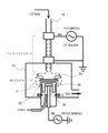
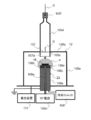
- FIG. 13 is a schematic view showing a plasma processing apparatus according to the first embodiment related to the present invention.
- FIG. 14 is an explanatory view showing a state where the wafer is being etched by the plasma processing apparatus.
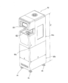
- 15A and 15B are external views showing a housing in which the plasma processing apparatus is accommodated.
- FIG. 15A is a front view
- FIG. 15B is a right side view
- FIG. 15C is a rear view.
- FIG. 16 is a schematic perspective view showing a nozzle used in the plasma processing apparatus.
- the plasma processing apparatus M is a minimal plasma etching based on a minimal fabrication concept accommodated in a case 102 having a standardized size.
- this minimal fab concept is optimal for the semiconductor manufacturing market with a small amount of various products, and can cope with various fabs that save resources, save energy, save investment, and have high performance.
- JP 2012-54414 A This realizes a minimal production system that minimizes the production described in 1.
- the casing 102 is a module formed in a substantially rectangular parallelepiped shape having a longitudinal direction in the vertical direction, and has a structure that blocks each of fine particles and gas molecules to the inside.
- a plasma processing apparatus M for plasma etching the wafer 18 is accommodated in a main body Ma as an upper part of the apparatus on the upper side of the casing 102.
- the plasma etching by the plasma processing apparatus M the surface of the wafer 18 is etched corresponding to the resist pattern laminated on the surface of the wafer 18.
- a supply section 103a for supplying, for example, an etching gas G used for plasma etching in the plasma processing apparatus M.
- the etching gas G is generated outside the housing 102 and then supplied into the plasma processing apparatus M through the supply unit 103a.
- a control storage unit Mb as a lower part of the apparatus for incorporating a control device for controlling the plasma processing apparatus M in the main body part Ma is provided below the casing 102.
- a cooling unit 109, a power supply unit 110, and the like used for etching in the plasma processing apparatus M are stored.
- a discharge unit 103b serving as an outlet for discharging a gas such as an etching gas G after being used for etching in the plasma processing apparatus M to the outside of the housing 102 is provided. Yes.
- this discharge part 103b is connected to the tank (not shown) etc. which store the gas discharged
- the front side of the main body part Ma is formed in a shape in which the front side of the main body part Ma is cut out in a concave shape upward in the middle part of the main body part Ma of the housing 102.
- An operation panel 81 is attached to the upper front side of the main body portion Ma.
- the lower part of the main body Ma is a front chamber Mc for carrying the wafer 18 into the housing 102.
- a substantially circular docking port 82 as a shuttle accommodating portion for installing a minimal shuttle (not shown) as a transfer container is provided at a substantially central portion of the upper surface of the front chamber Mc.
- the front chamber Mc is configured to block each of fine particles and gas molecules into the housing 102. That is, the front chamber Mc is a PLAD (Particle Lock Air-tight Docking) system that allows the wafer 18 accommodated in the minimal shuttle to be taken into and out of the housing 102 without being exposed to the outside air. ing.
- the wafer 18 carried in from the docking port 82 is transferred to a predetermined position of the plasma processing apparatus M, and the wafer 18 after being etched in the plasma processing apparatus M is docked.
- a conveying device (not shown) for carrying out to is accommodated.
- this transfer device for example, a workpiece transfer device described in JP 2011-96942 A is used.
- the plasma processing apparatus M is accommodated in a plasma processing chamber 12 as a wafer processing chamber at the upper rear side of the front chamber Mc in the housing 102.
- the wafer 18 to be etched by the plasma processing apparatus M has a circular surface with a predetermined size, for example, a diameter of 12.5 mm (half inch size), and is made of single crystal silicon (Si). It is formed in a disk shape.
- a predetermined resist pattern is formed on the surface of the wafer 18 in advance and is in a state before plasma etching.
- the plasma processing apparatus M is a combination of a so-called LF microplasma method and a stage RF plasma method. That is, the plasma processing apparatus M generates a large amount of fluorine radicals (F) in the etching gas G by applying a low frequency voltage to an LF application unit 108 attached to a gas supply pipe 105d described later, and supports the wafer. Along with positive ions (CF 3 + , Ar + ) that are ionized by applying high frequency voltage to the RF application plate 106 d attached to the table 22 to generate an ion sheath and exciting CF 4 and Ar in the etching gas G A large amount of fluorine radicals (F) are struck almost vertically into the surface of the wafer 18 for vertical etching.
- CF 3 + , Ar + positive ions
- the plasma processing apparatus M includes a plasma processing chamber 12 as a chamber and a wafer support 22 as a stage installed in the plasma processing chamber 12.
- the support base 22 is airtightly covered with the plasma processing chamber 12.
- the plasma processing chamber 12 is made of a transparent material to which a low frequency voltage can be applied from the outside such as quartz glass.
- the plasma processing chamber 12 has a cylindrical main body portion 105a, and the main body portion 105a is installed along the vertical direction.
- the upper end side of the main body portion 105a is connected to a disk-shaped upper plate 105b.
- the shape is closed.
- a rectangular opening 105c is formed at the center position of the upper plate 105b, and the lower end side of, for example, a rectangular tube-shaped gas supply pipe 105d as a gas supply unit is concentric with the opening 105c. It is fitted and attached to the shape.
- the gas supply pipe 105d is formed in a rectangular cross-sectional shape having an outer dimension that is smaller than the inner dimension of the main body 105a and slightly larger than the outer dimension of the wafer 18, and a part of the lower end side of the gas supply pipe 105d
- the opening 105c is fitted into the opening 105c from the outside of the upper plate 105b, and is integrally attached to the opening 105c by welding or the like.
- the shape of the gas supply pipe 105d may be a shape other than a rectangular tube shape, for example, a cylindrical shape.
- a block-like nozzle 107 is fitted and attached to the lower end of the gas supply pipe 105d.
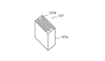
- the nozzle 107 includes a prismatic main body 107a having an outer dimension substantially equal to the inner dimension of the gas supply pipe 105d.
- the main body 107 a is formed such that the longitudinal dimension of the end face in the vertical direction is slightly larger than the outer diameter dimension of the wafer 18. Further, as shown in FIG. 16, a plurality of gas insertion holes 107b are formed in the main body portion 107a.
- These gas insertion holes 107b are formed in a straight line along the height direction of the main body portion 107a, and the gas insertion holes 107b are in a state of being spaced apart in parallel and at equal intervals, from one end surface of the main body portion 107a. The other end surface is provided so as to penetrate linearly. That is, these gas insertion holes 107b are provided over the entire nozzle 107, and the etching gas G is blown onto the wafer 18 substantially uniformly by passing through the gas insertion holes 107b of the nozzle 107. Yes.
- a gas supply port 105e is joined to the upper part of the gas supply pipe 105d.
- the gas supply port 105e is formed by concentrically reducing the diameter of the upper end of the gas supply pipe 105d, and a branch pipe (not shown) is provided in the gas supply pipe 105d.
- a metal tube 105f is attached to the gas supply port 105e, and a mixed gas (CF 4 / CF) of, for example, carbon tetrafluoride and argon (Ar) is supplied from the gas supply port 105e via the metal tube 105f.
- An etching gas G such as Ar
- the etching gas G it can be a gas that is composed of only carbon tetrafluoride (CF 4).
- the gas supply pipe 105d generates nozzle plasma for generating microplasma (microplasma having a diameter of the order of ⁇ m to mm) M in the etching gas G sprayed on the wafer 18 through the gas supply pipe 105d.
- An LF application unit 108 as a unit is provided.
- the LF application unit 108 is a radical generation unit that generates microplasma MP in the etching gas G sprayed from the nozzle 107 to the wafer 18 and generates a large amount of fluorine radicals (F) derived from the microplasma MP.
- the LF application unit 108 includes electrode portions 108a and 108b attached to the upper side and the lower side of the portion protruding upward from the upper plate 105b of the gas supply pipe 105d.
- the lower electrode portion 108b is attached to the lower edge portion of the portion protruding upward from the upper plate 105b of the gas supply pipe 105d.
- These electrode portions 108a and 108b are formed in a coil shape by winding a copper wire in the circumferential direction around the gas supply pipe 105d.
- a low-frequency power source 110a is attached between the electrode portions 108a and 108b, and a high-voltage low-frequency voltage is applied from the low-frequency power source 110a to the electrode portions 108a and 108b.
- Microplasma MP is generated in the etching gas G passing through the gas supply pipe 105d. That is, the high-voltage low-frequency voltage applied between the electrodes 108a and 108b of the LF application unit 108 is a dielectric barrier discharge that generates a high-voltage AC excited plasma in the etching gas G.
- the voltage is 10 kVp-p, Frequency: An AC high voltage of about 8 kHz is considered to be a main factor in generating microplasma MP.
- the wafer support 22 is housed in the plasma processing chamber 12, and is installed vertically below the opening 105 c of the plasma processing chamber 12, along the axial direction of the plasma processing chamber 12. That is, the wafer support base 22 has an RF application plate 106d, which will be described later, concentrically positioned with respect to the gas supply port 105e of the plasma processing chamber 12, and is spaced downward from the gas supply port 105e by a predetermined distance. In place. That is, the wafer support base 22 does not directly contact the RF application plate 106d on the wafer support base 22 with the microplasma MP that may blow out from the gas supply port 105e of the plasma processing chamber 12 through the nozzle 107.
- the plasma processing chamber 12 is attached with a certain interval.
- the wafer support base 22 includes a cylindrical main body portion 106a, and is installed in a state where the axial direction of the main body portion 106a is along the vertical direction.
- the upper end surface of the main body portion 106a is closed to form a flat disk-shaped installation surface 106b, and the wafer 18 is installed on the installation surface 106b. That is, the main body portion 106 a is formed to have an outer diameter dimension slightly larger than the outer diameter dimension of the wafer 18, and is an installation surface 106 b having a diameter dimension slightly larger than the outer diameter dimension of the wafer 18.
- the installation surface 106b includes an insulating plate 106c having an insulating property, and an RF application plate 106d, which is a lower electrode serving as a stage plasma generation unit, is laminated on the insulating plate 106c.
- the insulating plate 106c and the RF application plate 106d are each formed in a substantially disc shape, and the wafer 18 is placed on the RF application plate 106d.
- the RF application plate 106 d forms a vertical electric field E from the upper side to the lower side in the plasma processing chamber 12 together with the LF application unit 108 to generate an ion sheath in the plasma processing chamber 12 and onto the wafer 18.
- It is an ion assist part that generates plasma P in the etching gas G to be sent and excites the etching gas G to ionize it.
- the RF application plate 106d is applied with a high-frequency voltage (RF) such as 13.56 MHz, and plasma is applied to the region including the wafer 18 placed on the RF application plate 106d, that is, on and around the wafer 18. P is generated, and CF 4 and Ar constituting the etching gas G sprayed on the wafer 18 are excited to be ionized or radicalized to generate positive ions (CF 3 + , Ar + ) or fluorine radicals (F). To do. Further, an electrode portion 106e is provided at the center portion on the lower end side of the RF application plate 106d, and a high frequency voltage is applied from the high frequency power source 110b installed outside the plasma processing chamber 12 through the electrode portion 106e.
- RF high-frequency voltage
- a cooling unit 109 as a cooling unit for cooling the wafer 18 placed on the RF application plate 106 d of the wafer support 22 is attached to the wafer support 22.
- the cooling unit 109 is, for example, a water-cooling type, and is installed on the RF application plate 106d by cooling the RF application plate 106d through the main body 106a and the insulating plate 106c of the wafer support base 22.
- the wafer 18 is cooled.
- the cooling unit 109 is housed and attached in the control housing portion Mb.
- the power supply unit 110 includes a low frequency power supply 110a and a high frequency power supply 110b.
- a lid 111a for closing the lower end of the plasma processing chamber 12 is attached below the plasma processing chamber 12, and the lid 111a is evacuated for evacuating the plasma processing chamber 12.
- a vacuum forming device 111 as a part is attached.
- the vacuum forming device 111 is also housed and attached in the control housing portion Mb, and the plasma is formed in a state where the wafer 18 is placed on the RF application plate 106 d of the wafer support 22 in the plasma processing chamber 12.
- the inside of the processing chamber 12 is evacuated.
- a minimal shuttle accommodating the wafer 18 before etching is fitted into the docking port 82 of the front chamber Mc of the housing 102 and installed.
- a start switch (not shown) displayed on a predetermined position of the housing 102, for example, the operation panel 81 or the like is pressed.
- the cooling unit 109 is driven and cooling of the wafer support 22 is started.
- the minimal shuttle installed in the docking port 82 is opened, and the wafer 18 accommodated in the minimal shuttle is transferred onto the RF application plate 106d of the wafer support 22 of the plasma processing apparatus M by the transfer device. Installed. At this time, the wafer support base 22 is brought into a state in which the wafer support base 22 is taken out from the plasma processing chamber 12 by, for example, relatively moving the wafer support base 22 and the plasma processing chamber 12 up and down. Yes.
- the plasma processing chamber 12 of the plasma processing apparatus M is sealed with the lid 111a, and the vacuum forming apparatus 111 is evacuated until the inside of the plasma processing chamber 12 is almost vacuumed.
- the etching gas G is supplied into the plasma processing chamber 12 from the gas supply port 105e through the metal tube 105f attached to the gas supply port 105e of the plasma processing chamber 12, and the pressure in the plasma processing chamber 12 is reduced. A predetermined pressure is maintained.
- the low frequency power supply 110a is turned on to apply a low frequency voltage between the electrodes 108a and 108b of the LF application unit 108, and the high frequency power supply 110b is turned on and applied to the RF application plate 106d via the electrode unit 106e.
- a potential gradient along the direction toward the wafer 18 is formed in the plasma processing chamber 12, and a vertical electric field E is formed.
- the microplasma MP is caused to enter the etching gas G by the low frequency voltage applied between the electrodes 108a and 108b.
- the fluorine in CF 4 constituting the etching gas G is radicalized to generate a large amount of fluorine radicals (F). That is, CF 4 in the etching gas G is separated into CF 3 and F (CF 4 + e ⁇ CF 3 + F + e), and a large amount of fluorine radicals (F) are generated.
- the fluorine radicals pass through the gas insertion holes 107b of the nozzle 107 attached to the gas supply port 105e together with the etching gas G, so that the spraying direction is rectified substantially in parallel and sprayed onto the wafer 18 substantially evenly. It is done.
- a high frequency voltage applied to the RF application plate 106d of the wafer support 22 generates plasma P around the RF application plate 106d, and an electric field is formed around the RF application plate 106d along with an ion sheath along the vertical direction. E is formed.
- the fluorine radical (F) radicalized with the positive ions (CF 3 + , Ar + ) excited and ionized immediately before the etching gas G blown from the nozzle 107 is struck onto the wafer 18.
- the wafer 18 is subjected to plasma etching (isotropic etching) through a resist pattern that is struck vertically and is provided on the wafer 18.
- fluorine radicals (F) derived from the microplasma MP are produced by the low frequency voltage applied between the electrode portions 108a and 108b of the LF application unit 108 and the high frequency voltage applied to the RF application plate 106d.
- the reaction of the fluorine radical (F) with the single crystal silicon (Si) constituting the wafer 18 is made efficient, and positive charges such as Ar + and CF 3 + in the etching gas G are supplied. Ions (plus ions) are transferred onto the wafer 18, and the reaction of fluorine radicals (F) to the single crystal silicon (Si) constituting the wafer 18 is assisted to increase the efficiency. Crystalline silicon bonds (Si—Si) are cut and plasma etching is performed.
- the single crystal silicon (Si) and the fluorine radical (F) constituting the wafer 18 react (Si [solid] + 4F ⁇ SiF 4 [gas]).
- Surface plasma etching proceeds.
- Ar, CF 4, and the like in the etching gas G are excited and ionized (Ar + , CF 3 + ), and the single crystal silicon constituting the wafer 18 is ion-assisted by these positive ions.
- the reaction between (Si) and the fluorine radical (F) is promoted, and the etching reaction on the surface of the wafer 18 is promoted and speeded up.
- the sealing of the plasma processing chamber 12 is released, and the wafer support base 22 and the plasma processing chamber 12 are moved up and down relatively, for example, from within the plasma processing chamber 12.
- the wafer support base 22 is taken out, and the wafer 18 placed on the RF application plate 106d of the wafer support base 22 is placed on the minimal shuttle by a pull back operation by the transfer device, and then the minimal shuttle is closed.
- the wafer 18 is accommodated. Further, the wafer 18 is unloaded by removing the minimal shuttle accommodating the wafer 18 from the docking port 82 of the front chamber Mc. Thereafter, the driving of the cooling unit 109 is stopped, and the cooling of the wafer support 22 is stopped.
- the inside of the plasma processing chamber 12 is evacuated by the vacuum forming apparatus 111 in a state where the wafer 18 is placed on the RF application plate 106d of the wafer support 22.
- the etching gas G is supplied from the gas supply pipe 105 d into the plasma processing chamber 12.
- the large amount of fluorine radicals pass through the gas insertion holes 107b of the nozzle 107 together with the etching gas G, so that the blowing direction is rectified in a substantially vertical direction, and the densities of the fluorine radicals and the etching gas G are substantially uniform.
- the plasma P generated in the etching gas G existing on and around the wafer 18 placed on the RF application plate 106d by the high-frequency voltage applied to the RF application plate 106d of the wafer support 22 is generated.
- the radical (F) was struck almost vertically into the surface of the wafer 18 for etching.
- the effect of the gas flow of the etching gas ejected from the nozzle 107 is generated by generating the microplasma MP in the gas supply pipe 105d by the low frequency voltage applied between the electrodes 108a and 108b of the LF application unit 108.
- the fluorine radical (F) can be efficiently transported to the surface of the wafer, and the gas transport effect of the nozzle 107 is also added.
- the fluorine radical (F) derived from the microplasma MP is struck on the wafer 18 in large quantities.
- the high-frequency voltage applied to the RF application plate 106d of the wafer support 22 strikes the wafer 18 with positive ions such as CF 3 + and Ar + that have excited CF 4 and Ar in the etching gas G. be able to. Therefore, under the assistance of these positive ions, the reaction of fluorine radicals to the single crystal silicon (Si) constituting the wafer 18, that is, the cutting of the single crystal silicon bond (Si-Si) on the surface of the wafer 18 (plasma etching). It can be performed efficiently and at high speed.
- positive ions such as CF 3 + and Ar + that have excited CF 4 and Ar in the etching gas G. be able to. Therefore, under the assistance of these positive ions, the reaction of fluorine radicals to the single crystal silicon (Si) constituting the wafer 18, that is, the cutting of the single crystal silicon bond (Si-Si) on the surface of the wafer 18 (plasma etching). It can be performed efficiently and at high speed.
- the wafer 18 installed on the RF application plate 106d of the wafer support 22 is cooled by the cooling unit 109, and the nozzle 107 for spraying the etching gas G onto the wafer 18 is provided from the RF application plate 106d.
- the microplasma MP generated in the gas supply pipe 105d does not directly hit the wafer 18, resist damage due to plasma irradiation is prevented, and a large amount of fluorine radicals (F) generated in the gas supply pipe 105d are prevented.
- the etching gas G is struck onto the wafer 18 together with the large amount of fluorine radicals, the temperature rise of the wafer 18 can be appropriately suppressed, and for example, seizure of the resist pattern laminated on the wafer 18 can be prevented. Therefore, the wafer 18 can be etched with higher accuracy.
- the etching gas G passes through the gas insertion holes 107b of the nozzle 107, the etching gas G is rectified with the blowing direction of the etching gas G being substantially parallel. 18 can be struck almost evenly. Further, the plasma P is generated in the etching gas G existing on and around the wafer 18 placed on the RF application plate 106d by the high-frequency voltage applied to the RF application plate 106d of the wafer support 22 to perform etching.
- the etching gas G can be efficiently excited and ionized and radicalized immediately before the gas G is struck against the wafer 18. Therefore, since the etching gas G sprayed from the nozzle 107 to the wafer 18 can be ionized and radicalized more efficiently, even a relatively small half-inch wafer 18 can be etched with high accuracy.
- the density of the etching gas G that has passed through each gas insertion hole 107b of the nozzle 107 is substantially uniform. Since the etching gas G can be evenly sprayed onto the wafer 18, the wafer 18 can be etched with high accuracy using the nozzle 107 having a relatively simple configuration.
- the configuration is such that the etching gas G supplied from the gas supply pipe 105d is sprayed substantially uniformly onto the wafer 18 by the nozzle 107 in which the plurality of gas insertion holes 107b are provided in parallel and at equal intervals.
- the gas insertion hole 107b can also be used as the nozzle 107 in which a plurality of cylindrical pipe bodies 112 each having a gas insertion hole 107b opened at the center are integrated at equal intervals. Can be sprayed on the wafer 18 substantially evenly.
- the nozzle 107 that can etch the wafer 18 with high accuracy can be made simpler.
- the gas supply pipe 105d of the plasma processing chamber 12 is formed into a tubular shape having a plurality of gas supply holes (not shown), or a plurality of nozzles 107 are attached to the gas supply ports 105e of the gas supply pipe 105d. It can also be configured.
- a high etching rate of about 500 nm / min at the maximum, so that it is possible to process the wafer 18 that is clearly technically superior to the case of the second embodiment described later. It is.
- FIG. 18 is a schematic view showing a plasma processing apparatus according to the second embodiment related to the present invention.
- the second embodiment is different from the first embodiment described above in that the first embodiment has a configuration in which an RF application plate 106d for applying a high-frequency voltage to the wafer 18 placed on the wafer support 22 is provided.
- the RF application plate 106d is not provided, and the wafer 18 is plasma-etched using only high-pressure AC excited plasma. That is, in the plasma processing apparatus M according to the second embodiment, as shown in FIG. 18, the plasma processing chamber 12 is configured similarly to the first embodiment, but the structure of the wafer support 22 is different from that of the first embodiment. To do. Specifically, in the wafer support base 22, an insulating plate 106c is installed on the installation surface 106b, and the wafer 18 is installed on the insulating plate 6c.
- the cooling unit 109 is driven to start cooling the wafer support 22 and the wafer 18 is placed on the insulating plate 106 c of the wafer support 22. Thereafter, similarly to the first embodiment, the plasma processing chamber 12 is sealed, and the inside of the plasma processing chamber 12 is evacuated by the vacuum forming device 111. In this state, after the etching gas G is supplied into the plasma processing chamber 12 from the gas supply port 105e of the plasma processing chamber 12, the low-frequency power source 110a is turned on and the low-frequency power is supplied between the electrodes 108a and 108b of the LF applying unit 108. A voltage is applied.
- the microplasma MP is generated in the etching gas G by the low frequency voltage applied between the electrodes 108a and 108b. Is done. At this time, CF 4 in the etching gas G is separated into CF 3 and F, and a large amount of fluorine radicals (F) are generated.
- the etching gas G is rectified in a substantially parallel manner when passing through each gas insertion hole 107b of the nozzle 107, and is blown substantially evenly onto the wafer 18, and a resist pattern provided on the wafer 18 is removed. Then, the wafer 18 is plasma etched. At this time, on the surface of the wafer 18, the single crystal silicon (Si) and the fluorine radical (F) constituting the wafer 18 react (Si [solid] + 4F ⁇ SiF 4 [gas]). Surface plasma etching proceeds.
- the second configuration configured as described above can generate the microplasma MP in the etching gas G by the low frequency voltage applied between the electrode portions 108a and 108b of the LF applying portion 108 attached to the plasma processing chamber 12, and the nozzle
- the blowing direction of the etching gas G is rectified to be substantially parallel, and a large amount of fluorine radicals (F) can be struck on the wafer 18 almost uniformly.
- the wafer 18 can be accurately etched through the provided resist pattern.
- the etching rate is 5 to 10 ⁇ m / min
- the plasma density is high
- the plasma column is ejected.
- the wafer 18 is directly irradiated and the resist pattern on the wafer 18 may be damaged.
- it is not suitable for etching the wafer 18 on which the resist pattern is laminated local etching of a single crystal silicon bare wafer or the like is possible.
- the etching rate is low and about 30 nm / min, but it can be applied to the etching of the wafer 18 on which the resist pattern is laminated.
- the heat generation of the wafer 18 is small and the resist resistance of the resist pattern can be maintained.
- the resist pattern may be deteriorated, so that there is a possibility that it takes time to remove the resist pattern (ashing).
- the microplasma MP diffuses downstream of the gas supply pipe 105d, and fluorine radicals can be supplied to the surface of the wafer 18, so that the resist pattern The stacked wafers 18 can be etched.
- the distance between the gas supply pipe 105d and the wafer 18 is too close (for example, less than 5 mm), the resist pattern on the wafer 18 may be damaged.
- FIG. 19 is a schematic view showing a part of a plasma processing apparatus according to the third embodiment of the present invention.
- the third embodiment relating to the present invention differs from the first embodiment described above in that the first embodiment is a fixed wafer support base 22 whereas the third embodiment is a movable wafer support base 22.
- the wafer support 22 is moved to scan the wafer 18. That is, in the plasma processing apparatus M according to the third embodiment, the configuration other than the wafer support base 22 is the same as that of the first embodiment, and the structure of the wafer support base 22 is the first configuration as shown in FIG. Is different.
- the wafer support 22 includes a wafer holder 161 on which the wafer 18 is placed.
- the wafer holder 161 is provided with a scanning mechanism 160 as a scanning unit including an X-axis stage 162 that moves the wafer holder 161 in the X-axis direction and a Y-axis stage 163 that moves the wafer holder 161 in the Y-axis direction.
- the scanning mechanism 160 moves the wafer holder 161 in each of the X-axis direction and the Y-axis direction that intersect the direction in which the etching gas G is blown from the nozzle 107.
- a linear motor 164 is attached to the X-axis stage 162 as a drive source for moving the wafer holder 161 in the X-axis direction via the X-axis stage 162.
- a linear motor 165 is also attached to the Y-axis stage 163 as a drive source for moving the wafer holder 161 in the Y-axis direction via the Y-axis stage 163.
- the driving of the linear motors 164 and 165 of the scan mechanism 160 is appropriately controlled to perform wafer etching.
- the etching point on 18 is scanned in the X-axis direction and the Y-axis direction.
- the wafer to be plasma-etched is large, it is impossible to scan and scan the wafer during plasma etching.
- the plasma processing apparatus M targets a circular wafer 18 having a diameter of 12.5 mm (half inch size), the wafer 18 can be scanned during plasma etching, and the etching rate in the surface of the wafer 18 can be measured. Can be made uniform.
- FIG. 20 is a schematic view showing a plasma processing apparatus according to the fourth embodiment related to the present invention.
- FIG. 21 is an explanatory diagram showing a state where the wafer is being etched by the plasma processing apparatus.
- the fourth mode is different from the first mode described above in that the first mode is a configuration in which the LF application unit 108 is provided in the gas supply pipe 105d of the plasma processing chamber 12, whereas the fourth mode is Without the LF application unit 108, the wafer is plasma-etched only with the stage RF plasma. That is, in the plasma processing apparatus M according to the fourth embodiment, as shown in FIG. 20, the wafer support base 22 is configured similarly to the first embodiment, but the structure of the plasma processing chamber 12 is different from that of the first embodiment. To do. Specifically, the gas supply pipe 105d of the plasma processing chamber 12 is not provided with the electrode portions 108a and 108b of the LF application section 108. The etching gas supplied from the gas supply pipe 105d and passed through the nozzle 107 is used. G is sprayed onto the wafer 18 installed on the RF application plate 106 d of the wafer support 22.
- the cooling unit 109 is driven to start cooling the wafer support 22 and the wafer 18 is placed on the RF application plate 106 d of the wafer support 22. Thereafter, similarly to the first embodiment, the plasma processing chamber 12 is sealed, and the inside of the plasma processing chamber 12 is evacuated by the vacuum forming device 111. In this state, after the etching gas G is supplied into the plasma processing chamber 12 from the gas supply port 105e of the plasma processing chamber 12, the high frequency power supply 110b is turned on and a high frequency voltage is applied to the RF application plate 106d via the electrode portion 106e. Is done.
- the blowing direction of the etching gas G is rectified substantially in parallel and sprayed onto the wafer 18.
- the etching gas G generates a plasma P in the etching gas G by a high frequency voltage applied to the RF application plate 106 d of the wafer support 22, and the wafer 18 passes through the resist pattern provided on the wafer 18. Is plasma etched.
- CF 4 in the etching gas G is separated into CF 3 and F by the high frequency voltage applied to the RF application plate 106 d, and fluorine radicals (F) are generated.
- argon gas, CF 4, etc. in the etching gas G are ionized (Ar + , CF 3 + ), and silicon (Si) and fluorine constituting the wafer 18 are ion-assisted by these positive ions. Reaction with the radical (F) (Si [solid] + 4F ⁇ SiF 4 [gas]) is promoted, and the etching reaction on the surface of the wafer 18 is promoted.
- the plasma P can be generated in the etching gas G by the high frequency voltage applied to the RF application plate 106 d of the wafer support 22, and when passing through each gas insertion hole 107 b of the nozzle 107.
- the etching direction can be rectified substantially parallel to each other, and the etching gas G can be sprayed onto the wafer 18 substantially evenly. Therefore, the wafer 18 can be accurately etched through the resist pattern provided on the wafer 18.
- the plasma P when the pressure in the plasma processing chamber 12 is higher than 2 kPa, the plasma P cannot be generated in the plasma processing chamber 12, so that the plasma processing chamber 12 is discharged. It must be evacuated to a pressure of 2 kPa or less where possible. That is, when the pressure in the plasma processing chamber 12 is 2 kPa or less and the etching rate is about 150 nm / min at the maximum, if the wafer 18 is cooled by the cooling unit 109, the wafer 18 on which the resist pattern is laminated is etched. It becomes possible. On the other hand, when the wafer 18 is not cooled by the cooling unit 109, resist resistance is poor and the resist pattern may be deteriorated, so that there is a possibility that it takes time to remove (ash) the resist pattern.
- the wafer 18 on which the resist pattern is laminated is etched by applying a low peripheral voltage between at least the electrodes 108a and 108b of the LF applying unit 108.
- each form is not limited to this, and other than the single crystal silicon structure wafer 18 on which a resist pattern is laminated can be used correspondingly.
- the gas supply pipe 105d can be moved with respect to the plasma processing chamber 12, and the gas supply pipe 105d is scanned in the horizontal direction to scan the wafer 18, or the gas supply pipe 105d has a large diameter, and a plurality of By attaching the nozzle 107 and rectifying the etching gas G, even a large-diameter wafer larger than a half-inch size minimal wafer can be used correspondingly.
- FIG. 22 is a schematic view showing a plasma processing apparatus M according to Embodiments 1 to 6 of the present invention.
- 23A and 23B are diagrams illustrating scanning conditions of the wafer 18 by the plasma processing apparatus M according to the first to sixth embodiments, where FIG. 23A is a distance R movement from the initial position O, and FIG. 23B is a rotational scanning with a radius R. .
- a nozzle 107 having an outer diameter of 6 mm and an inner diameter of 4 mm is used, and the pressure in the plasma processing chamber 12 is set to 180 Pa.
- the low frequency power supply 110a applies a low frequency voltage of 8 kHz between the electrodes
- the high frequency power supply 110b applies a high frequency voltage of 13.56 MHz to the RF application plate 106d, while the cooling unit 109 applies RF.
- the plate 106d is cooled.
- the scanning condition by the scanning mechanism 160 is a linear velocity V when the radius (distance) R is about 4 mm from the initial position (center position) O of the wafer 18. Is 2 mm / s, and the wafer 18 is rotationally scanned (no rotation of the wafer 18).
- a wafer 18 having an outer diameter of 12.5 mm is used, and a range from the outer peripheral edge of the wafer 18 to 0.5 mm is pressed by a clamp 24 to be a holding allowance, and 5 mm from the center position O of the wafer 18.
- the etching rate is measured every 1 mm in the region up to.
- Example 1 As a result, as shown in FIG. 12A, in Example 1, a small convex etching rate distribution was obtained with an average etching rate of about 10 nm / min. In Example 2, an etching rate distribution on the surface of the flat wafer 18 of about 40 nm / min was obtained. In Example 3, although the etching rate distribution has a Gaussian distribution shape, the average etching rate of Example 3 is larger than the sum of the etching rates of Example 1 and Example 2, and is 98.1 nm. / Min, and a clearly large etching rate could be obtained.
- the wafer 18 can be etched at a higher speed when each of the microplasma and the RF is turned on.
- the etching rate non-uniformity was as large as 22.7%.
- Example 5 when the wafer 18 is scanned by the scan mechanism 160 while only microplasma is turned on (Example 4), when the wafer 18 is scanned by the scan mechanism 160 while only RF is turned on (implementation) Example 5)
- the etching rate [nm] with respect to the position (position) [mm] of the wafer 18 / Min] was measured.
- the average etching rate of Example 6 is as high as 78.8 nm / min compared to the etching rates of Example 4 and Example 5, and the non-uniformity is 3. Compared to Example 3 above, 5% was clearly smaller. Therefore, it was found that the wafer 18 can be etched more accurately by scanning the wafer 18 while turning on each of the microplasma W and RF.
Landscapes
- Physics & Mathematics (AREA)
- Engineering & Computer Science (AREA)
- Plasma & Fusion (AREA)
- Chemical & Material Sciences (AREA)
- Analytical Chemistry (AREA)
- Drying Of Semiconductors (AREA)
- Container, Conveyance, Adherence, Positioning, Of Wafer (AREA)
- Plasma Technology (AREA)
- Physical Vapour Deposition (AREA)
- Chemical Vapour Deposition (AREA)
Abstract
Description
図13は、本発明に関連する第1形態に係るプラズマ処理装置を示す概略図ある。図14は、プラズマ処理装置にてウエハをエッチングしている状態を示す説明図である。図15は、プラズマ処理装置が収容される筐体を示す外観図で、(a)は正面図、(b)は右側面図、(c)は背面図である。図16は、プラズマ処理装置に使用されるノズルを示す概略斜視図である。
次いで、プラズマ処理装置Mは、筐体102内の前室Mcの後側上部のウエハ処理室としてのプラズマ処理室12内に収容されている。そして、このプラズマ処理装置Mにてエッチングするウエハ18は、所定の大きさ、例えば直径12.5mm(ハーフインチサイズ)の円形状の表面を有し、単結晶シリコン(Si)にて構成された円盤状に形成されている。そして、このウエハ18の表面には、予め所定のレジストパターンが形成され、プラズマエッチング前の状態とされている。
プラズマ処理室12は、例えば石英ガラス等の外部から低周波電圧を印加することが可能な透明な材料にて構成されている。そして、このプラズマ処理室12は、円筒状の本体部105aを有し、この本体部105aの軸方向を上下方向に沿わせて設置され、この本体部105aの上端側が円盤状の上板105bにて閉塞された形状とされている。また、この上板105bの中心位置には、矩形状の開口部105cが形成されており、この開口部105cには、ガス供給部としての、例えば角筒状のガス供給管105dの下端側が同心状に嵌合されて取り付けられている。このガス供給管105dは、本体部105aの内寸法より小さく、ウエハ18の外寸法より若干大きな外寸法を有する断面矩形筒状に形成されており、このガス供給管105dの下端側の一部を上板105bの外側から開口部105cに内嵌合させた状態とされ、この開口部105cに溶接等されて一体的に取り付けられている。ここで、ガス供給管105dの形状としては、角筒状以外の形状、例えば円筒状等であってもよい。
ウエハ支持台22は、プラズマ処理室12内に収容されつつ、このプラズマ処理室12の上下方向に軸方向を沿わせつつ、このプラズマ処理室12の開口部105cの鉛直下に設置されている。すなわち、このウエハ支持台22は、後述するRF印加板106dを、プラズマ処理室12のガス供給口105eに対し同心状に位置させつつ、このガス供給口105eから所定間隔ほど下方に間隔を空けた位置に設置されている。すなわち、このウエハ支持台22は、プラズマ処理室12のガス供給口105eからノズル107を介して吹き出してくるおそれのあるマイクロプラズマMPが、ウエハ支持台22上のRF印加板106dへ直接当たない程度の間隔を空けてプラズマ処理室12内に取り付けられている。
図18は、本発明に関連する第2形態に係るプラズマ処理装置を示す概略図である。
図19は、本発明の第3形態に係るプラズマ処理装置の一部を示す概略図である。
図20は、本発明に関連する第4形態に係るプラズマ処理装置を示す概略図である。図21は、プラズマ処理装置にてウエハをエッチングしている状態を示す説明図である。
なお、上記各形態では、少なくともLF印加部108の電極部108a,108b間への低周電圧の印加を用いて、レジストパターンが積層されたウエハ18をエッチングする構成とした。しかしながら、各形態はこれに限定されることはなく、レジストパターンが積層された単結晶シリコン構造のウエハ18以外であっても、対応させて用いることができる。
14 ゲートバルブ
15 ガス供給口
16 ガス排出口
18 半導体ウエハ(ワーク)
19 ウエハ支持装置
20 ウエハ受台
22、22’ ウエハ支持台
24 ウエハ押さえ板
25 案内溝
26 スプリング用溝
26a スプリング
28 保護管
30 冷媒供給管(冷媒供給部)
32 冷却管
34、34’給電体(給電部)
35 下部電極
36 ウエハ保持溝(ウエハ載置部)
38 アーム用溝
39 凹部
40 冷却口
41 通気口
42 排気孔
43 上孔
44 上部リング
46 下部リング
48 外筒
50 第1駆動板
52 第1モータ
54 第1駆動ねじ
56 第2駆動板
58 第2モータ
60 第2駆動ねじ
62 昇降装置
63 Z軸方向駆動板
64 絶縁スペーサ
66 内部導体
67 外部導体
68 絶縁体
69 外部電極
70 可動ワッシャ(遮蔽部材)
82 ドッキングポート
M プラズマ処理装置
Ma 本体部
Mb 制御収納部
Mc 前室
Claims (10)
- 処理対象のウエハを支持するウエハ支持装置と、前記ウエハ支持装置の上部に設けられたウエハ保持部と、前記ウエハ保持部を収納し、外気から実質的に遮断された処理室と、前記処理室内に設けられたウエハ処理部と、を有するミニマルファブシステム用処理装置であって、
前記ウエハ支持装置は、前記ウエハ保持部と、前記ウエハ保持部を支持して前記処理室外へ延長する軸部と、前記処理室外で前記軸部に接続し、前記軸部をXYZ軸方向に移動する駆動部と、前記ウエハ処理部による処理がウエハ全面にわたり均一となるように前記駆動部を制御する制御装置と、を有し、
前記駆動部の作動により、前記ウエハ保持部に保持されたウエハが、前記処理室内の前記ウエハ処理部に対しウエハ全面にわたり相対的に移動可能とされている
ことを特徴とするミニマルファブシステム用処理装置。 - 前記処理室の底部には、前記軸部がXYZ軸方向に移動可能な範囲の穴が設けられており、前記穴による前記処理室と前記軸部との間隙をふさぐ遮蔽部材が、前記ウエハ保持部のXYZ方向への移動を妨げないように設けられている
ことを特徴とする請求項1に記載のミニマルファブシステム用処理装置。 - 前記遮蔽部材が、開口径の異なる複数の可動ワッシャからなる
ことを特徴とする請求項2に記載のミニマルファブシステム用処理装置。 - 前記ウエハ保持部は、ウエハ受台とウエハ支持台とウエハ押さえ板とを有し、
前記ウエハ受台は、前記処理室内へ搬送された前記ウエハを載置するウエハ載置部を有し、
前記ウエハ支持台は、前記軸部の上端部に設けられ、前記軸部が前記駆動部によって上昇するに伴い前記ウエハ載置部に載置された前記ウエハを前記ウエハ押さえ板に押しつけるように昇降し、
前記ウエハ押さえ板は、上昇する前記ウエハの周辺部を押さえて、前記ウエハ支持台と協働して前記ウエハを固定して支持する
ことを特徴とする請求項1~3のいずれかに記載のミニマルファブシステム用処理装置。 - 前記ウエハ処理部は、前記処理室へマイクロプラズマを供給するマイクロプラズマ発生部と、前記処理室内に設けられ、供給された前記マイクロプラズマに高周波を重畳するRFプラズマ発生部と、を有するプラズマ処理部であって、
前記ウエハ支持装置は、前記軸部内に、前記RFプラズマ発生部へ給電する給電部と、前記ウエハおよび前記給電部の冷却のための冷媒を供給する冷媒供給部とが設けられている
ことを特徴とする請求項1~4のいずれかに記載のミニマルファブシステム用処理装置。 - 前記ウエハ支持装置の前記軸部は、外側が前記ウエハ受台を支持する保護管とされ、前記保護管内部に、前記ウエハ支持台を支持する冷媒供給管が設けられて前記冷媒供給部とされ、
前記冷媒供給管は、前記保護管の内部でその軸方向に自由に移動できるように前記ウエハ支持台を支持しており、
前記冷媒供給管の内部には、不活性ガスおよび前記不活性ガスを冷却するための冷媒を収容した冷却管と、前記RFプラズマ発生部に給電するための給電体とが収容されている
ことを特徴とする請求項5に記載のミニマルファブシステム用処理装置。 - 前記冷却管は前記給電体を取り巻くように配置され、前記冷却管の内部には、前記駆動部側から前記RFプラズマ発生装置の電極側に供給されて再び駆動部側に戻るように冷媒が供給される
ことを特徴とする請求項6に記載のミニマルファブシステム用処理装置。 - 前記給電部は、外管と、前記外管の内部に設けられる内管の二重構造となって前記ウエハ支持台を支持し、前記給電部の上端に前記RFプラズマ発生部の電極が接続されてなり、
前記内管の内部空間と、前記内管と前記外管の空隙空間とが連通して冷却用冷媒の通路が構成されており、前記給電部および前記電極を冷却する
ことを特徴とする請求項5~7のいずれかに記載のミニマルファブシステム用処理装置。 - 前記処理室の底部には前記穴を囲む上部リングが取り付けられ、前記ウエハ受台を支持する前記保護管は前記上部リングを貫通して前記処理室の外部に延長されており、前記上部リングにはフレキシブルに変形する外筒を挟んで下部リングが接続されており、
前記保護管は前記外筒を貫通して、前記下部リングとともに前記駆動部にその一端を接続固定され、前記駆動部は前記下部リングに固定されて前記冷媒供給管の下端を支持し、
前記冷媒供給管に支持された前記ウエハ支持台は、前記ウエハを支持固定するために、前記駆動部によって前記保護管の軸方向に移動し、
前記保護管は、前記駆動部によって前記保護管の軸と交差する方向にスキャニング移動する
ことを特徴とする請求項6~8のいずれかに記載のミニマルファブシステム用処理装置。 - 前記ウエハをハーフインチサイズの半導体ウエハとし、前記ウエハ処理部がプラズマ処理部である
ことを特徴とする請求項1~9のいずれかに記載のミニマルファブシステム用処理装置。
Priority Applications (2)
| Application Number | Priority Date | Filing Date | Title |
|---|---|---|---|
| US15/126,087 US20170098557A1 (en) | 2014-03-14 | 2015-03-10 | Plasma processing device |
| JP2016507770A JP6465442B2 (ja) | 2014-03-14 | 2015-03-10 | プラズマ処理装置 |
Applications Claiming Priority (2)
| Application Number | Priority Date | Filing Date | Title |
|---|---|---|---|
| JP2014052630 | 2014-03-14 | ||
| JP2014-052630 | 2014-03-14 |
Publications (1)
| Publication Number | Publication Date |
|---|---|
| WO2015137364A1 true WO2015137364A1 (ja) | 2015-09-17 |
Family
ID=54071807
Family Applications (1)
| Application Number | Title | Priority Date | Filing Date |
|---|---|---|---|
| PCT/JP2015/057067 Ceased WO2015137364A1 (ja) | 2014-03-14 | 2015-03-10 | プラズマ処理装置 |
Country Status (3)
| Country | Link |
|---|---|
| US (1) | US20170098557A1 (ja) |
| JP (1) | JP6465442B2 (ja) |
| WO (1) | WO2015137364A1 (ja) |
Cited By (5)
| Publication number | Priority date | Publication date | Assignee | Title |
|---|---|---|---|---|
| US20170338080A1 (en) * | 2016-05-19 | 2017-11-23 | Plasmotica, LLC | Apparatus and method for programmable spatially selective nanoscale surface functionalization |
| JP2020063471A (ja) * | 2018-10-16 | 2020-04-23 | Jswアフティ株式会社 | プラズマ成膜装置およびプラズマ成膜方法 |
| JP2020170655A (ja) * | 2019-04-04 | 2020-10-15 | 日本電産株式会社 | プラズマ処理装置用の治具、および、プラズマ処理システム |
| JP2021527299A (ja) * | 2018-06-08 | 2021-10-11 | アプライド マテリアルズ インコーポレイテッドApplied Materials,Incorporated | プラズマ化学気相堆積チャンバ内の寄生プラズマを抑制する装置 |
| JP2024000574A (ja) * | 2022-06-21 | 2024-01-09 | 国立大学法人東北大学 | 半導体装置の製造方法および半導体製造装置 |
Families Citing this family (3)
| Publication number | Priority date | Publication date | Assignee | Title |
|---|---|---|---|---|
| CN110148549A (zh) * | 2019-06-19 | 2019-08-20 | 深圳市诚峰智造有限公司 | 等离子处理装置 |
| CN111900085A (zh) * | 2020-08-18 | 2020-11-06 | 上海华力微电子有限公司 | 去胶方法 |
| CN115938903B (zh) * | 2022-12-01 | 2025-09-26 | 中国原子能科学研究院 | 支撑机构和离子源 |
Citations (4)
| Publication number | Priority date | Publication date | Assignee | Title |
|---|---|---|---|---|
| JPS58168230A (ja) * | 1982-03-30 | 1983-10-04 | Fujitsu Ltd | マイクロ波プラズマ処理方法 |
| JPS61212023A (ja) * | 1985-03-18 | 1986-09-20 | Hitachi Ltd | ドライエッチング装置 |
| JPS62143426A (ja) * | 1985-12-18 | 1987-06-26 | Hitachi Ltd | 光照射装置 |
| JP2005203490A (ja) * | 2004-01-14 | 2005-07-28 | Hitachi High-Technologies Corp | プラズマ処理装置及び電極 |
Family Cites Families (8)
| Publication number | Priority date | Publication date | Assignee | Title |
|---|---|---|---|---|
| US4487089A (en) * | 1981-12-18 | 1984-12-11 | Rockwell International Corporation | Miniature adjustable potentiometer clutch |
| DE3803411A1 (de) * | 1988-02-05 | 1989-08-17 | Leybold Ag | Vorrichtung zur halterung von werkstuecken |
| US4797053A (en) * | 1988-02-16 | 1989-01-10 | Huntington Mechanical Laboratories, Inc. | Manipulator for vacuum applications |
| US5540821A (en) * | 1993-07-16 | 1996-07-30 | Applied Materials, Inc. | Method and apparatus for adjustment of spacing between wafer and PVD target during semiconductor processing |
| JP3612158B2 (ja) * | 1996-11-18 | 2005-01-19 | スピードファム株式会社 | プラズマエッチング方法及びその装置 |
| US20080190558A1 (en) * | 2002-04-26 | 2008-08-14 | Accretech Usa, Inc. | Wafer processing apparatus and method |
| US20040255442A1 (en) * | 2003-06-19 | 2004-12-23 | Mcdiarmid James | Methods and apparatus for processing workpieces |
| JP2013021382A (ja) * | 2011-07-07 | 2013-01-31 | Toshiba Corp | 同軸ケーブル |
-
2015
- 2015-03-10 US US15/126,087 patent/US20170098557A1/en not_active Abandoned
- 2015-03-10 JP JP2016507770A patent/JP6465442B2/ja active Active
- 2015-03-10 WO PCT/JP2015/057067 patent/WO2015137364A1/ja not_active Ceased
Patent Citations (4)
| Publication number | Priority date | Publication date | Assignee | Title |
|---|---|---|---|---|
| JPS58168230A (ja) * | 1982-03-30 | 1983-10-04 | Fujitsu Ltd | マイクロ波プラズマ処理方法 |
| JPS61212023A (ja) * | 1985-03-18 | 1986-09-20 | Hitachi Ltd | ドライエッチング装置 |
| JPS62143426A (ja) * | 1985-12-18 | 1987-06-26 | Hitachi Ltd | 光照射装置 |
| JP2005203490A (ja) * | 2004-01-14 | 2005-07-28 | Hitachi High-Technologies Corp | プラズマ処理装置及び電極 |
Cited By (11)
| Publication number | Priority date | Publication date | Assignee | Title |
|---|---|---|---|---|
| US20170338080A1 (en) * | 2016-05-19 | 2017-11-23 | Plasmotica, LLC | Apparatus and method for programmable spatially selective nanoscale surface functionalization |
| US10497541B2 (en) | 2016-05-19 | 2019-12-03 | Nedal Saleh | Apparatus and method for programmable spatially selective nanoscale surface functionalization |
| US10832895B2 (en) | 2016-05-19 | 2020-11-10 | Plasmotica, LLC | Stand alone microfluidic analytical chip device |
| JP2021527299A (ja) * | 2018-06-08 | 2021-10-11 | アプライド マテリアルズ インコーポレイテッドApplied Materials,Incorporated | プラズマ化学気相堆積チャンバ内の寄生プラズマを抑制する装置 |
| JP7333346B2 (ja) | 2018-06-08 | 2023-08-24 | アプライド マテリアルズ インコーポレイテッド | プラズマ化学気相堆積チャンバ内の寄生プラズマを抑制する装置 |
| JP2020063471A (ja) * | 2018-10-16 | 2020-04-23 | Jswアフティ株式会社 | プラズマ成膜装置およびプラズマ成膜方法 |
| JP7329913B2 (ja) | 2018-10-16 | 2023-08-21 | Jswアフティ株式会社 | プラズマ成膜方法 |
| JP2020170655A (ja) * | 2019-04-04 | 2020-10-15 | 日本電産株式会社 | プラズマ処理装置用の治具、および、プラズマ処理システム |
| JP7215305B2 (ja) | 2019-04-04 | 2023-01-31 | 日本電産株式会社 | プラズマ処理装置用の治具、および、プラズマ処理システム |
| JP2024000574A (ja) * | 2022-06-21 | 2024-01-09 | 国立大学法人東北大学 | 半導体装置の製造方法および半導体製造装置 |
| JP7832429B2 (ja) | 2022-06-21 | 2026-03-18 | 国立大学法人東北大学 | 半導体装置の製造方法および半導体製造装置 |
Also Published As
| Publication number | Publication date |
|---|---|
| JP6465442B2 (ja) | 2019-02-06 |
| US20170098557A1 (en) | 2017-04-06 |
| JPWO2015137364A1 (ja) | 2017-04-06 |
Similar Documents
| Publication | Publication Date | Title |
|---|---|---|
| JP6465442B2 (ja) | プラズマ処理装置 | |
| TWI795589B (zh) | 處理微電子工件的方法、以及處理基板的方法 | |
| US20100098882A1 (en) | Plasma source for chamber cleaning and process | |
| JP5510437B2 (ja) | プラズマ処理装置及びプラズマ処理方法 | |
| US9818582B2 (en) | Plasma processing method | |
| JP6832858B2 (ja) | 非熱ソフトプラズマ洗浄 | |
| US9583313B2 (en) | Plasma processing apparatus and plasma processing method | |
| CN105470125A (zh) | 处理基板的系统和方法 | |
| KR20140092257A (ko) | 플라즈마 처리 방법 및 플라즈마 처리 장치 | |
| WO2014065034A1 (ja) | プラズマ処理装置及び方法 | |
| KR101232198B1 (ko) | 플라스마 발생 유닛 및 이를 포함하는 기판 처리 장치 및 방법 | |
| JP5232512B2 (ja) | プラズマ処理装置及びプラズマ処理方法 | |
| US8342121B2 (en) | Plasma processing apparatus | |
| JP6043968B2 (ja) | プラズマ処理方法並びに電子デバイスの製造方法 | |
| JP6292470B2 (ja) | ノズル式のプラズマエッチング装置 | |
| JP7304067B2 (ja) | ノズルプラズマ装置 | |
| US20070228008A1 (en) | Medium pressure plasma system for removal of surface layers without substrate loss | |
| JP6127276B2 (ja) | プラズマ処理装置及び方法 | |
| JP6288702B2 (ja) | ステージ式のプラズマエッチング装置 | |
| JP5857207B2 (ja) | プラズマ処理装置及び方法 | |
| KR20140046065A (ko) | 플라즈마 처리 장치 및 방법 | |
| KR20220083923A (ko) | 기판 처리 장치 | |
| TW202514711A (zh) | 利用氣靜壓軸承的基板蝕刻 | |
| WO2007067177A1 (en) | Medium pressure plasma system for removal of surface layers without substrate loss | |
| JP2016119313A (ja) | プラズマ処理装置 |
Legal Events
| Date | Code | Title | Description |
|---|---|---|---|
| 121 | Ep: the epo has been informed by wipo that ep was designated in this application |
Ref document number: 15761843 Country of ref document: EP Kind code of ref document: A1 |
|
| ENP | Entry into the national phase |
Ref document number: 2016507770 Country of ref document: JP Kind code of ref document: A |
|
| NENP | Non-entry into the national phase |
Ref country code: DE |
|
| WWE | Wipo information: entry into national phase |
Ref document number: 15126087 Country of ref document: US |
|
| 122 | Ep: pct application non-entry in european phase |
Ref document number: 15761843 Country of ref document: EP Kind code of ref document: A1 |