WO2015137278A1 - 感光性導電フィルム - Google Patents
感光性導電フィルム Download PDFInfo
- Publication number
- WO2015137278A1 WO2015137278A1 PCT/JP2015/056832 JP2015056832W WO2015137278A1 WO 2015137278 A1 WO2015137278 A1 WO 2015137278A1 JP 2015056832 W JP2015056832 W JP 2015056832W WO 2015137278 A1 WO2015137278 A1 WO 2015137278A1
- Authority
- WO
- WIPO (PCT)
- Prior art keywords
- conductive
- photosensitive
- conductive film
- meth
- layer
- Prior art date
Links
- 239000000835 fiber Substances 0.000 claims abstract description 106
- 150000001875 compounds Chemical class 0.000 claims description 46
- NIXOWILDQLNWCW-UHFFFAOYSA-M Acrylate Chemical compound [O-]C(=O)C=C NIXOWILDQLNWCW-UHFFFAOYSA-M 0.000 claims description 38
- ZJCCRDAZUWHFQH-UHFFFAOYSA-N Trimethylolpropane Chemical compound CCC(CO)(CO)CO ZJCCRDAZUWHFQH-UHFFFAOYSA-N 0.000 claims description 20
- BQCADISMDOOEFD-UHFFFAOYSA-N Silver Chemical group [Ag] BQCADISMDOOEFD-UHFFFAOYSA-N 0.000 claims description 17
- 125000002887 hydroxy group Chemical group [H]O* 0.000 claims description 17
- 229910052709 silver Inorganic materials 0.000 claims description 17
- 239000004332 silver Substances 0.000 claims description 17
- IAYPIBMASNFSPL-UHFFFAOYSA-N Ethylene oxide Chemical compound C1CO1 IAYPIBMASNFSPL-UHFFFAOYSA-N 0.000 claims description 11
- GOOHAUXETOMSMM-UHFFFAOYSA-N Propylene oxide Chemical compound CC1CO1 GOOHAUXETOMSMM-UHFFFAOYSA-N 0.000 claims description 6
- WMYINDVYGQKYMI-UHFFFAOYSA-N 2-[2,2-bis(hydroxymethyl)butoxymethyl]-2-ethylpropane-1,3-diol Chemical compound CCC(CO)(CO)COCC(CC)(CO)CO WMYINDVYGQKYMI-UHFFFAOYSA-N 0.000 claims description 4
- WXZMFSXDPGVJKK-UHFFFAOYSA-N pentaerythritol Chemical compound OCC(CO)(CO)CO WXZMFSXDPGVJKK-UHFFFAOYSA-N 0.000 claims description 4
- 239000010408 film Substances 0.000 description 118
- 239000011347 resin Substances 0.000 description 64
- 229920005989 resin Polymers 0.000 description 64
- 229920000642 polymer Polymers 0.000 description 41
- 238000000034 method Methods 0.000 description 40
- 239000011230 binding agent Substances 0.000 description 39
- 239000000758 substrate Substances 0.000 description 25
- -1 acryloxy Chemical group 0.000 description 18
- 239000006185 dispersion Substances 0.000 description 16
- 238000000576 coating method Methods 0.000 description 14
- 238000001035 drying Methods 0.000 description 14
- 125000001997 phenyl group Chemical group [H]C1=C([H])C([H])=C(*)C([H])=C1[H] 0.000 description 14
- LYCAIKOWRPUZTN-UHFFFAOYSA-N Ethylene glycol Chemical compound OCCO LYCAIKOWRPUZTN-UHFFFAOYSA-N 0.000 description 12
- ATUOYWHBWRKTHZ-UHFFFAOYSA-N Propane Chemical compound CCC ATUOYWHBWRKTHZ-UHFFFAOYSA-N 0.000 description 12
- 239000011248 coating agent Substances 0.000 description 12
- 239000007788 liquid Substances 0.000 description 12
- 239000000203 mixture Substances 0.000 description 12
- 125000004432 carbon atom Chemical group C* 0.000 description 11
- 239000004020 conductor Substances 0.000 description 11
- 239000007787 solid Substances 0.000 description 10
- 125000003944 tolyl group Chemical group 0.000 description 10
- ZWEHNKRNPOVVGH-UHFFFAOYSA-N 2-Butanone Chemical compound CCC(C)=O ZWEHNKRNPOVVGH-UHFFFAOYSA-N 0.000 description 9
- 239000000178 monomer Substances 0.000 description 9
- DAKWPKUUDNSNPN-UHFFFAOYSA-N Trimethylolpropane triacrylate Chemical compound C=CC(=O)OCC(CC)(COC(=O)C=C)COC(=O)C=C DAKWPKUUDNSNPN-UHFFFAOYSA-N 0.000 description 8
- 125000000217 alkyl group Chemical group 0.000 description 8
- 125000003178 carboxy group Chemical group [H]OC(*)=O 0.000 description 8
- 238000006243 chemical reaction Methods 0.000 description 8
- 239000003999 initiator Substances 0.000 description 8
- 238000005259 measurement Methods 0.000 description 8
- 238000002360 preparation method Methods 0.000 description 8
- 230000008569 process Effects 0.000 description 8
- 239000011342 resin composition Substances 0.000 description 8
- 239000000126 substance Substances 0.000 description 8
- CERQOIWHTDAKMF-UHFFFAOYSA-N Methacrylic acid Chemical compound CC(=C)C(O)=O CERQOIWHTDAKMF-UHFFFAOYSA-N 0.000 description 7
- 238000011156 evaluation Methods 0.000 description 7
- 238000004519 manufacturing process Methods 0.000 description 7
- XLYOFNOQVPJJNP-UHFFFAOYSA-N water Substances O XLYOFNOQVPJJNP-UHFFFAOYSA-N 0.000 description 7
- CSCPPACGZOOCGX-UHFFFAOYSA-N Acetone Chemical compound CC(C)=O CSCPPACGZOOCGX-UHFFFAOYSA-N 0.000 description 6
- 239000004925 Acrylic resin Substances 0.000 description 6
- ZHNUHDYFZUAESO-UHFFFAOYSA-N Formamide Chemical compound NC=O ZHNUHDYFZUAESO-UHFFFAOYSA-N 0.000 description 6
- 230000005540 biological transmission Effects 0.000 description 6
- 230000015572 biosynthetic process Effects 0.000 description 6
- 239000001294 propane Substances 0.000 description 6
- 239000004698 Polyethylene Substances 0.000 description 5
- 239000003513 alkali Substances 0.000 description 5
- 239000000470 constituent Substances 0.000 description 5
- 238000010030 laminating Methods 0.000 description 5
- 239000000463 material Substances 0.000 description 5
- 229910052751 metal Inorganic materials 0.000 description 5
- 239000002184 metal Substances 0.000 description 5
- 229920000573 polyethylene Polymers 0.000 description 5
- 229920000139 polyethylene terephthalate Polymers 0.000 description 5
- 239000005020 polyethylene terephthalate Substances 0.000 description 5
- PPBRXRYQALVLMV-UHFFFAOYSA-N Styrene Chemical compound C=CC1=CC=CC=C1 PPBRXRYQALVLMV-UHFFFAOYSA-N 0.000 description 4
- IISBACLAFKSPIT-UHFFFAOYSA-N bisphenol A Chemical compound C=1C=C(O)C=CC=1C(C)(C)C1=CC=C(O)C=C1 IISBACLAFKSPIT-UHFFFAOYSA-N 0.000 description 4
- 230000008859 change Effects 0.000 description 4
- 239000003795 chemical substances by application Substances 0.000 description 4
- 230000000052 comparative effect Effects 0.000 description 4
- 125000002496 methyl group Chemical group [H]C([H])([H])* 0.000 description 4
- 239000003960 organic solvent Substances 0.000 description 4
- 238000003756 stirring Methods 0.000 description 4
- 238000002834 transmittance Methods 0.000 description 4
- DLKQHBOKULLWDQ-UHFFFAOYSA-N 1-bromonaphthalene Chemical compound C1=CC=C2C(Br)=CC=CC2=C1 DLKQHBOKULLWDQ-UHFFFAOYSA-N 0.000 description 3
- TXBCBTDQIULDIA-UHFFFAOYSA-N 2-[[3-hydroxy-2,2-bis(hydroxymethyl)propoxy]methyl]-2-(hydroxymethyl)propane-1,3-diol Chemical compound OCC(CO)(CO)COCC(CO)(CO)CO TXBCBTDQIULDIA-UHFFFAOYSA-N 0.000 description 3
- 229920000178 Acrylic resin Polymers 0.000 description 3
- IJGRMHOSHXDMSA-UHFFFAOYSA-N Atomic nitrogen Chemical compound N#N IJGRMHOSHXDMSA-UHFFFAOYSA-N 0.000 description 3
- 239000004593 Epoxy Substances 0.000 description 3
- 229910052782 aluminium Inorganic materials 0.000 description 3
- XAGFODPZIPBFFR-UHFFFAOYSA-N aluminium Chemical compound [Al] XAGFODPZIPBFFR-UHFFFAOYSA-N 0.000 description 3
- 239000012298 atmosphere Substances 0.000 description 3
- 230000008901 benefit Effects 0.000 description 3
- QUZSUMLPWDHKCJ-UHFFFAOYSA-N bisphenol A dimethacrylate Chemical class C1=CC(OC(=O)C(=C)C)=CC=C1C(C)(C)C1=CC=C(OC(=O)C(C)=C)C=C1 QUZSUMLPWDHKCJ-UHFFFAOYSA-N 0.000 description 3
- 125000000753 cycloalkyl group Chemical group 0.000 description 3
- 238000011161 development Methods 0.000 description 3
- 230000018109 developmental process Effects 0.000 description 3
- 229910001873 dinitrogen Inorganic materials 0.000 description 3
- 239000003822 epoxy resin Substances 0.000 description 3
- 238000005227 gel permeation chromatography Methods 0.000 description 3
- 230000014509 gene expression Effects 0.000 description 3
- 239000011261 inert gas Substances 0.000 description 3
- 229940059574 pentaerithrityl Drugs 0.000 description 3
- 229920000647 polyepoxide Polymers 0.000 description 3
- 238000010992 reflux Methods 0.000 description 3
- 230000035945 sensitivity Effects 0.000 description 3
- 239000003381 stabilizer Substances 0.000 description 3
- 238000007740 vapor deposition Methods 0.000 description 3
- 125000000954 2-hydroxyethyl group Chemical group [H]C([*])([H])C([H])([H])O[H] 0.000 description 2
- OKTJSMMVPCPJKN-UHFFFAOYSA-N Carbon Chemical compound [C] OKTJSMMVPCPJKN-UHFFFAOYSA-N 0.000 description 2
- NPKSPKHJBVJUKB-UHFFFAOYSA-N N-phenylglycine Chemical compound OC(=O)CNC1=CC=CC=C1 NPKSPKHJBVJUKB-UHFFFAOYSA-N 0.000 description 2
- XYFCBTPGUUZFHI-UHFFFAOYSA-N Phosphine Chemical compound P XYFCBTPGUUZFHI-UHFFFAOYSA-N 0.000 description 2
- WYURNTSHIVDZCO-UHFFFAOYSA-N Tetrahydrofuran Chemical compound C1CCOC1 WYURNTSHIVDZCO-UHFFFAOYSA-N 0.000 description 2
- 238000007754 air knife coating Methods 0.000 description 2
- 150000001408 amides Chemical class 0.000 description 2
- 125000003118 aryl group Chemical group 0.000 description 2
- 239000002041 carbon nanotube Substances 0.000 description 2
- 229910021393 carbon nanotube Inorganic materials 0.000 description 2
- 238000013329 compounding Methods 0.000 description 2
- 238000007796 conventional method Methods 0.000 description 2
- 238000010586 diagram Methods 0.000 description 2
- 238000007607 die coating method Methods 0.000 description 2
- 239000012153 distilled water Substances 0.000 description 2
- PCHJSUWPFVWCPO-UHFFFAOYSA-N gold Chemical compound [Au] PCHJSUWPFVWCPO-UHFFFAOYSA-N 0.000 description 2
- 239000010931 gold Substances 0.000 description 2
- 229910052737 gold Inorganic materials 0.000 description 2
- 238000007756 gravure coating Methods 0.000 description 2
- 238000002156 mixing Methods 0.000 description 2
- BASFCYQUMIYNBI-UHFFFAOYSA-N platinum Chemical compound [Pt] BASFCYQUMIYNBI-UHFFFAOYSA-N 0.000 description 2
- 238000004917 polyol method Methods 0.000 description 2
- 229920001451 polypropylene glycol Polymers 0.000 description 2
- 238000003672 processing method Methods 0.000 description 2
- 238000007650 screen-printing Methods 0.000 description 2
- 238000005507 spraying Methods 0.000 description 2
- 238000003860 storage Methods 0.000 description 2
- 239000004094 surface-active agent Substances 0.000 description 2
- 239000010409 thin film Substances 0.000 description 2
- RNFJDJUURJAICM-UHFFFAOYSA-N 2,2,4,4,6,6-hexaphenoxy-1,3,5-triaza-2$l^{5},4$l^{5},6$l^{5}-triphosphacyclohexa-1,3,5-triene Chemical compound N=1P(OC=2C=CC=CC=2)(OC=2C=CC=CC=2)=NP(OC=2C=CC=CC=2)(OC=2C=CC=CC=2)=NP=1(OC=1C=CC=CC=1)OC1=CC=CC=C1 RNFJDJUURJAICM-UHFFFAOYSA-N 0.000 description 1
- SMZOUWXMTYCWNB-UHFFFAOYSA-N 2-(2-methoxy-5-methylphenyl)ethanamine Chemical compound COC1=CC=C(C)C=C1CCN SMZOUWXMTYCWNB-UHFFFAOYSA-N 0.000 description 1
- NIXOWILDQLNWCW-UHFFFAOYSA-N 2-Propenoic acid Natural products OC(=O)C=C NIXOWILDQLNWCW-UHFFFAOYSA-N 0.000 description 1
- 101710134784 Agnoprotein Proteins 0.000 description 1
- 229920002799 BoPET Polymers 0.000 description 1
- 229920000049 Carbon (fiber) Polymers 0.000 description 1
- 206010034972 Photosensitivity reaction Diseases 0.000 description 1
- 229920001609 Poly(3,4-ethylenedioxythiophene) Polymers 0.000 description 1
- 239000002202 Polyethylene glycol Substances 0.000 description 1
- 239000004743 Polypropylene Substances 0.000 description 1
- 239000004793 Polystyrene Substances 0.000 description 1
- XUIMIQQOPSSXEZ-UHFFFAOYSA-N Silicon Chemical compound [Si] XUIMIQQOPSSXEZ-UHFFFAOYSA-N 0.000 description 1
- 238000005411 Van der Waals force Methods 0.000 description 1
- HVVWZTWDBSEWIH-UHFFFAOYSA-N [2-(hydroxymethyl)-3-prop-2-enoyloxy-2-(prop-2-enoyloxymethyl)propyl] prop-2-enoate Chemical compound C=CC(=O)OCC(CO)(COC(=O)C=C)COC(=O)C=C HVVWZTWDBSEWIH-UHFFFAOYSA-N 0.000 description 1
- DHKHKXVYLBGOIT-UHFFFAOYSA-N acetaldehyde Diethyl Acetal Natural products CCOC(C)OCC DHKHKXVYLBGOIT-UHFFFAOYSA-N 0.000 description 1
- 239000002253 acid Substances 0.000 description 1
- 150000008065 acid anhydrides Chemical class 0.000 description 1
- 125000000641 acridinyl group Chemical class C1(=CC=CC2=NC3=CC=CC=C3C=C12)* 0.000 description 1
- 150000001252 acrylic acid derivatives Chemical class 0.000 description 1
- 125000003647 acryloyl group Chemical group O=C([*])C([H])=C([H])[H] 0.000 description 1
- 239000000654 additive Substances 0.000 description 1
- 229920000180 alkyd Polymers 0.000 description 1
- 150000001448 anilines Chemical class 0.000 description 1
- 239000002518 antifoaming agent Substances 0.000 description 1
- 229940027998 antiseptic and disinfectant acridine derivative Drugs 0.000 description 1
- 238000013459 approach Methods 0.000 description 1
- 150000008365 aromatic ketones Chemical class 0.000 description 1
- 238000007611 bar coating method Methods 0.000 description 1
- 239000002585 base Substances 0.000 description 1
- 125000001797 benzyl group Chemical group [H]C1=C([H])C([H])=C(C([H])=C1[H])C([H])([H])* 0.000 description 1
- 238000011088 calibration curve Methods 0.000 description 1
- 239000003990 capacitor Substances 0.000 description 1
- 239000004917 carbon fiber Substances 0.000 description 1
- 239000003638 chemical reducing agent Substances 0.000 description 1
- 229920001577 copolymer Polymers 0.000 description 1
- 125000000332 coumarinyl group Chemical class O1C(=O)C(=CC2=CC=CC=C12)* 0.000 description 1
- 239000003431 cross linking reagent Substances 0.000 description 1
- 125000001511 cyclopentyl group Chemical group [H]C1([H])C([H])([H])C([H])([H])C([H])(*)C1([H])[H] 0.000 description 1
- 239000000539 dimer Substances 0.000 description 1
- 230000000694 effects Effects 0.000 description 1
- 238000010292 electrical insulation Methods 0.000 description 1
- 239000003480 eluent Substances 0.000 description 1
- 230000032050 esterification Effects 0.000 description 1
- 238000005886 esterification reaction Methods 0.000 description 1
- 150000002148 esters Chemical class 0.000 description 1
- 238000005530 etching Methods 0.000 description 1
- 125000001495 ethyl group Chemical group [H]C([H])([H])C([H])([H])* 0.000 description 1
- 239000000945 filler Substances 0.000 description 1
- 239000003063 flame retardant Substances 0.000 description 1
- 239000003205 fragrance Substances 0.000 description 1
- 238000010438 heat treatment Methods 0.000 description 1
- 239000001257 hydrogen Substances 0.000 description 1
- 229910052739 hydrogen Inorganic materials 0.000 description 1
- 239000012216 imaging agent Substances 0.000 description 1
- 229910003437 indium oxide Inorganic materials 0.000 description 1
- PJXISJQVUVHSOJ-UHFFFAOYSA-N indium(iii) oxide Chemical compound [O-2].[O-2].[O-2].[In+3].[In+3] PJXISJQVUVHSOJ-UHFFFAOYSA-N 0.000 description 1
- AMGQUBHHOARCQH-UHFFFAOYSA-N indium;oxotin Chemical compound [In].[Sn]=O AMGQUBHHOARCQH-UHFFFAOYSA-N 0.000 description 1
- 239000003112 inhibitor Substances 0.000 description 1
- 230000003993 interaction Effects 0.000 description 1
- 230000001678 irradiating effect Effects 0.000 description 1
- LAPRIVJANDLWOK-UHFFFAOYSA-N laureth-5 Chemical compound CCCCCCCCCCCCOCCOCCOCCOCCOCCO LAPRIVJANDLWOK-UHFFFAOYSA-N 0.000 description 1
- 239000004973 liquid crystal related substance Substances 0.000 description 1
- 229910021645 metal ion Inorganic materials 0.000 description 1
- 239000012299 nitrogen atmosphere Substances 0.000 description 1
- HMMGMWAXVFQUOA-UHFFFAOYSA-N octamethylcyclotetrasiloxane Chemical compound C[Si]1(C)O[Si](C)(C)O[Si](C)(C)O[Si](C)(C)O1 HMMGMWAXVFQUOA-UHFFFAOYSA-N 0.000 description 1
- 239000003921 oil Substances 0.000 description 1
- 125000000962 organic group Chemical group 0.000 description 1
- 150000002916 oxazoles Chemical class 0.000 description 1
- 230000003647 oxidation Effects 0.000 description 1
- 238000007254 oxidation reaction Methods 0.000 description 1
- 230000002093 peripheral effect Effects 0.000 description 1
- 239000005011 phenolic resin Substances 0.000 description 1
- 229910000073 phosphorus hydride Inorganic materials 0.000 description 1
- 230000036211 photosensitivity Effects 0.000 description 1
- 239000004014 plasticizer Substances 0.000 description 1
- 229910052697 platinum Inorganic materials 0.000 description 1
- 229920000767 polyaniline Polymers 0.000 description 1
- 229920006289 polycarbonate film Polymers 0.000 description 1
- 229920001223 polyethylene glycol Polymers 0.000 description 1
- 229920001155 polypropylene Polymers 0.000 description 1
- 229920002223 polystyrene Polymers 0.000 description 1
- 229920000036 polyvinylpyrrolidone Polymers 0.000 description 1
- 239000001267 polyvinylpyrrolidone Substances 0.000 description 1
- 235000013855 polyvinylpyrrolidone Nutrition 0.000 description 1
- 239000002244 precipitate Substances 0.000 description 1
- 238000007639 printing Methods 0.000 description 1
- 239000000047 product Substances 0.000 description 1
- 125000001436 propyl group Chemical group [H]C([*])([H])C([H])([H])C([H])([H])[H] 0.000 description 1
- 230000001681 protective effect Effects 0.000 description 1
- 230000009467 reduction Effects 0.000 description 1
- 230000007261 regionalization Effects 0.000 description 1
- 238000001878 scanning electron micrograph Methods 0.000 description 1
- 229910052710 silicon Inorganic materials 0.000 description 1
- 239000010703 silicon Substances 0.000 description 1
- 239000002109 single walled nanotube Substances 0.000 description 1
- 239000002904 solvent Substances 0.000 description 1
- 125000001424 substituent group Chemical group 0.000 description 1
- 239000006228 supernatant Substances 0.000 description 1
- 238000012360 testing method Methods 0.000 description 1
- YLQBMQCUIZJEEH-UHFFFAOYSA-N tetrahydrofuran Natural products C=1C=COC=1 YLQBMQCUIZJEEH-UHFFFAOYSA-N 0.000 description 1
- 229920002803 thermoplastic polyurethane Polymers 0.000 description 1
- 229920001187 thermosetting polymer Polymers 0.000 description 1
- 150000003577 thiophenes Chemical class 0.000 description 1
- XOLBLPGZBRYERU-UHFFFAOYSA-N tin dioxide Chemical compound O=[Sn]=O XOLBLPGZBRYERU-UHFFFAOYSA-N 0.000 description 1
- 229910001887 tin oxide Inorganic materials 0.000 description 1
Images


Classifications
-
- G—PHYSICS
- G03—PHOTOGRAPHY; CINEMATOGRAPHY; ANALOGOUS TECHNIQUES USING WAVES OTHER THAN OPTICAL WAVES; ELECTROGRAPHY; HOLOGRAPHY
- G03F—PHOTOMECHANICAL PRODUCTION OF TEXTURED OR PATTERNED SURFACES, e.g. FOR PRINTING, FOR PROCESSING OF SEMICONDUCTOR DEVICES; MATERIALS THEREFOR; ORIGINALS THEREFOR; APPARATUS SPECIALLY ADAPTED THEREFOR
- G03F7/00—Photomechanical, e.g. photolithographic, production of textured or patterned surfaces, e.g. printing surfaces; Materials therefor, e.g. comprising photoresists; Apparatus specially adapted therefor
- G03F7/004—Photosensitive materials
- G03F7/027—Non-macromolecular photopolymerisable compounds having carbon-to-carbon double bonds, e.g. ethylenic compounds
-
- G—PHYSICS
- G03—PHOTOGRAPHY; CINEMATOGRAPHY; ANALOGOUS TECHNIQUES USING WAVES OTHER THAN OPTICAL WAVES; ELECTROGRAPHY; HOLOGRAPHY
- G03F—PHOTOMECHANICAL PRODUCTION OF TEXTURED OR PATTERNED SURFACES, e.g. FOR PRINTING, FOR PROCESSING OF SEMICONDUCTOR DEVICES; MATERIALS THEREFOR; ORIGINALS THEREFOR; APPARATUS SPECIALLY ADAPTED THEREFOR
- G03F7/00—Photomechanical, e.g. photolithographic, production of textured or patterned surfaces, e.g. printing surfaces; Materials therefor, e.g. comprising photoresists; Apparatus specially adapted therefor
- G03F7/004—Photosensitive materials
- G03F7/0047—Photosensitive materials characterised by additives for obtaining a metallic or ceramic pattern, e.g. by firing
-
- G—PHYSICS
- G03—PHOTOGRAPHY; CINEMATOGRAPHY; ANALOGOUS TECHNIQUES USING WAVES OTHER THAN OPTICAL WAVES; ELECTROGRAPHY; HOLOGRAPHY
- G03F—PHOTOMECHANICAL PRODUCTION OF TEXTURED OR PATTERNED SURFACES, e.g. FOR PRINTING, FOR PROCESSING OF SEMICONDUCTOR DEVICES; MATERIALS THEREFOR; ORIGINALS THEREFOR; APPARATUS SPECIALLY ADAPTED THEREFOR
- G03F7/00—Photomechanical, e.g. photolithographic, production of textured or patterned surfaces, e.g. printing surfaces; Materials therefor, e.g. comprising photoresists; Apparatus specially adapted therefor
- G03F7/004—Photosensitive materials
- G03F7/027—Non-macromolecular photopolymerisable compounds having carbon-to-carbon double bonds, e.g. ethylenic compounds
- G03F7/028—Non-macromolecular photopolymerisable compounds having carbon-to-carbon double bonds, e.g. ethylenic compounds with photosensitivity-increasing substances, e.g. photoinitiators
- G03F7/031—Organic compounds not covered by group G03F7/029
-
- G—PHYSICS
- G03—PHOTOGRAPHY; CINEMATOGRAPHY; ANALOGOUS TECHNIQUES USING WAVES OTHER THAN OPTICAL WAVES; ELECTROGRAPHY; HOLOGRAPHY
- G03F—PHOTOMECHANICAL PRODUCTION OF TEXTURED OR PATTERNED SURFACES, e.g. FOR PRINTING, FOR PROCESSING OF SEMICONDUCTOR DEVICES; MATERIALS THEREFOR; ORIGINALS THEREFOR; APPARATUS SPECIALLY ADAPTED THEREFOR
- G03F7/00—Photomechanical, e.g. photolithographic, production of textured or patterned surfaces, e.g. printing surfaces; Materials therefor, e.g. comprising photoresists; Apparatus specially adapted therefor
- G03F7/004—Photosensitive materials
- G03F7/027—Non-macromolecular photopolymerisable compounds having carbon-to-carbon double bonds, e.g. ethylenic compounds
- G03F7/032—Non-macromolecular photopolymerisable compounds having carbon-to-carbon double bonds, e.g. ethylenic compounds with binders
- G03F7/033—Non-macromolecular photopolymerisable compounds having carbon-to-carbon double bonds, e.g. ethylenic compounds with binders the binders being polymers obtained by reactions only involving carbon-to-carbon unsaturated bonds, e.g. vinyl polymers
-
- G—PHYSICS
- G06—COMPUTING; CALCULATING OR COUNTING
- G06F—ELECTRIC DIGITAL DATA PROCESSING
- G06F3/00—Input arrangements for transferring data to be processed into a form capable of being handled by the computer; Output arrangements for transferring data from processing unit to output unit, e.g. interface arrangements
- G06F3/01—Input arrangements or combined input and output arrangements for interaction between user and computer
- G06F3/03—Arrangements for converting the position or the displacement of a member into a coded form
- G06F3/041—Digitisers, e.g. for touch screens or touch pads, characterised by the transducing means
- G06F3/044—Digitisers, e.g. for touch screens or touch pads, characterised by the transducing means by capacitive means
- G06F3/0445—Digitisers, e.g. for touch screens or touch pads, characterised by the transducing means by capacitive means using two or more layers of sensing electrodes, e.g. using two layers of electrodes separated by a dielectric layer
-
- G—PHYSICS
- G06—COMPUTING; CALCULATING OR COUNTING
- G06F—ELECTRIC DIGITAL DATA PROCESSING
- G06F3/00—Input arrangements for transferring data to be processed into a form capable of being handled by the computer; Output arrangements for transferring data from processing unit to output unit, e.g. interface arrangements
- G06F3/01—Input arrangements or combined input and output arrangements for interaction between user and computer
- G06F3/03—Arrangements for converting the position or the displacement of a member into a coded form
- G06F3/041—Digitisers, e.g. for touch screens or touch pads, characterised by the transducing means
- G06F3/044—Digitisers, e.g. for touch screens or touch pads, characterised by the transducing means by capacitive means
- G06F3/0446—Digitisers, e.g. for touch screens or touch pads, characterised by the transducing means by capacitive means using a grid-like structure of electrodes in at least two directions, e.g. using row and column electrodes
-
- G—PHYSICS
- G06—COMPUTING; CALCULATING OR COUNTING
- G06F—ELECTRIC DIGITAL DATA PROCESSING
- G06F2203/00—Indexing scheme relating to G06F3/00 - G06F3/048
- G06F2203/041—Indexing scheme relating to G06F3/041 - G06F3/045
- G06F2203/04103—Manufacturing, i.e. details related to manufacturing processes specially suited for touch sensitive devices
Definitions
- the present invention relates to a photosensitive conductive film, and more particularly to a photosensitive conductive film used for flat panel displays, touch screens, solar cells and the like.
- touch panels are used for large electronic devices such as personal computers and televisions; small electronic devices such as car navigation systems, mobile phones, portable music players, and electronic dictionaries; and display devices such as OA / FA devices.
- capacitive touch panel when the fingertip (conductor) contacts the touch input surface, the fingertip and the transparent electrode (transparent conductive film or the like) are capacitively coupled to form a capacitor.
- the capacitive touch panel detects the coordinates by capturing the change in the charge at the contact position of the fingertip.
- the projected capacitive touch panel has good operability because it can detect multiple points of the fingertip and can give complicated instructions.
- projection capacitive touch panels are increasingly used as input devices on the display surface of devices (such as mobile phones and portable music players) having small display devices because of their excellent operability.
- a plurality of X electrodes and a plurality of Y electrodes perpendicular to the X electrodes form a two-layer structure in order to express two-dimensional coordinates based on the X and Y axes. is doing.
- a transparent conductive film is used as the electrode.
- Patent Document 1 proposes a method for forming a conductive pattern using a photosensitive conductive film having a conductive layer containing conductive fibers.
- Patent Document 2 a method of forming a conductive pattern by laminating a photosensitive conductive film on a substrate, performing an exposure process twice, and subsequently developing is proposed.
- a wiring circuit for transmitting an electrical change generated in the transparent electrode portion to the control IC is formed in the peripheral frame region of the touch panel.
- a wiring circuit pattern is formed by printing a wiring circuit pattern by screen printing using a thermosetting or evaporative drying type silver paste, and is formed using a vapor deposited metal thin film. Wiring circuit and the like.
- a structure of a touch panel for example, a projected capacitive touch panel
- a structure in which a transparent electrode and a control IC are physically and electrically connected by a wiring circuit is common. In such a touch panel, if the connection between the wiring circuit and the transparent electrode is insufficient, there arises a problem that the touch panel does not operate normally.
- the conventional method has a problem that the resistance between the transparent electrode and the silver paste becomes unstable when the transparent electrode (sensor electrode, conductive pattern) and the control IC are connected by the silver paste printed wiring. Further, in the conventional technique, when the transparent electrode (sensor electrode, conductive pattern) and the control IC are connected by vapor deposition metal wiring, there is a problem that the connection between the transparent electrode and the vapor deposition metal cannot be established. Therefore, the transparent conductive film used as the transparent electrode is required to have excellent connectivity to the wiring circuit.
- An object of the present invention is to provide a photosensitive conductive film capable of obtaining a transparent conductive film having excellent connectivity to a wiring circuit.
- each of the conductive fibers included in the photosensitive layer includes:
- the average value of the shortest distance between the surface of the photosensitive layer and the support film is 0.1 to 50 nm, the resistance between the transparent conductive film (conductive pattern, etc.) and the wiring circuit is stably low.
- the connectivity of the transparent conductive film to the wiring circuit is improved.
- the photosensitive conductive film according to the present invention includes a support film and a photosensitive layer provided on the support film, and the photosensitive layer includes a plurality of conductive fibers, each of the conductive fibers, The average value of the shortest distance between the photosensitive layer and the surface on the support film side is 0.1 to 50 nm.
- a transparent conductive film having excellent connectivity to a wiring circuit can be obtained.
- Such a photosensitive conductive film can be used to produce a laminate having excellent connectivity between a wiring circuit and a transparent conductive film.
- the conductive fiber is preferably silver fiber. In this case, the conductivity of the formed transparent conductive film can be easily adjusted.
- the fiber diameter of the conductive fiber is preferably 1 to 50 nm.
- a transparent conductive film that is highly transparent to visible light can be formed.
- the fiber length of the conductive fiber is preferably 1 to 100 ⁇ m. In this case, a highly transparent and low resistance transparent conductive film can be easily formed by sufficiently ensuring contact between the conductive fibers.
- the photosensitive layer includes a photopolymerizable compound having an ethylenically unsaturated bond, and the hydroxyl value of the photopolymerizable compound is 90 mgKOH / g or less. Is preferred. In this case, it is easy to adjust the surface tension of the photosensitive layer.
- the photosensitive layer includes a photopolymerizable compound having an ethylenically unsaturated bond, and the critical surface tension of the photopolymerizable compound is 47 mN / m or less. It is preferable. In this case, it is easy to adjust the surface tension of the photosensitive layer.
- the photosensitive layer comprises trimethylolpropane tri (meth) acrylate, ethylene oxide-containing trimethylolpropane tri (meth) acrylate, propylene oxide-containing trimethylolpropane tri (meth) acrylate, ditrimethylolpropane tetra (meth) acrylate, and di It is preferable to include at least one selected from the group consisting of pentaerythritol hexa (meth) acrylate, and it is more preferable to include trimethylolpropane tri (meth) acrylate. In this case, a high-resolution transparent conductive pattern can be formed and the surface tension of the photosensitive layer can be easily adjusted.
- a transparent conductive film having excellent connectivity to a wiring circuit can be obtained.
- the conductive pattern (transparent conductive pattern) which has the outstanding connectivity with respect to a wiring circuit can be obtained.
- an application of a photosensitive conductive film for forming a transparent conductive film can be provided.
- ADVANTAGE OF THE INVENTION the application of the photosensitive conductive film for forming a conductive pattern (transparent conductive pattern) can be provided.
- ADVANTAGE OF THE INVENTION the application of the photosensitive conductive film for manufacturing a conductive pattern board
- ADVANTAGE OF THE INVENTION the application of the photosensitive conductive film for manufacturing a touch panel (for example, touch panel sensor) can be provided.
- FIG. 6 is a partial cross-sectional view taken along the line a-a ′ shown in FIG. 5.
- FIG. 6 is a partial cross-sectional view taken along the line b-b ′ shown in FIG. 5.
- FIG. 10 is a view showing a TEM photograph of a cross section of Comparative Example 3.
- (meth) acrylic acid means acrylic acid or methacrylic acid corresponding thereto.
- a or B only needs to include either A or B, and may include both.
- the materials exemplified below may be used alone or in combination of two or more unless otherwise specified.
- the content ratio of each component in the composition means the total amount of the plurality of substances present in the composition unless there is a particular notice when there are a plurality of substances corresponding to each component in the composition.
- the term “layer” includes a structure formed in a part in addition to a structure formed in the entire surface when observed as a plan view.
- the weight average molecular weight in this specification is a value measured by a gel permeation chromatography method (GPC) under the following conditions and converted by a calibration curve prepared using standard polystyrene.
- GPC conditions Pump: Hitachi L-6000 (manufactured by Hitachi, Ltd., trade name) Column: Gelpack GL-R440, Gelpack GL-R450, Gelpack GL-R400M (trade name, manufactured by Hitachi Chemical Co., Ltd.) Eluent: Tetrahydrofuran Measurement temperature: 40 ° C Flow rate: 2.05 ml / min Detector: Hitachi L-3300 type RI (manufactured by Hitachi, Ltd., trade name)
- FIGS. 1 and 2 show a photosensitive conductive film according to the present embodiment
- FIG. 1 is a partially cutaway perspective view showing the photosensitive conductive film
- FIG. 2 is taken along the line II-II in FIG. It is the schematic cross section along.
- a photosensitive conductive film 10 shown in FIGS. 1 and 2 includes a support film 1 and a photosensitive layer 4 provided on the support film 1.
- the photosensitive layer 4 has a conductive layer 2 provided on the support film 1 and a photosensitive resin layer 3 provided on the conductive layer 2.
- the support film 1 examples include a polyethylene terephthalate film (PET film), a polyethylene film, a polypropylene film, and a polycarbonate film.
- PET film polyethylene terephthalate film
- a polyethylene film is preferable from the viewpoint of excellent transparency or heat resistance.
- the thickness of the support film 1 is such that a conductive dispersion is applied (coating etc.) to form the conductive layer 2, and a photosensitive resin composition is applied (coating etc.) to form the photosensitive resin layer 3. ), Or from the viewpoint of preventing the support film from being broken in the step of peeling the support film before developing the exposed photosensitive layer 4, preferably 5 ⁇ m or more, more preferably 10 ⁇ m or more, and even more preferably 15 ⁇ m or more. .
- the thickness of the support film 1 is preferably 200 ⁇ m or less, more preferably 100 ⁇ m or less, and even more preferably 50 ⁇ m or less from the viewpoint of excellent resolution of the conductive pattern after the photosensitive layer 4 is exposed and developed. From these viewpoints, the thickness of the support film 1 is preferably 5 to 200 ⁇ m, more preferably 10 to 100 ⁇ m, and further preferably 15 to 50 ⁇ m.
- the conductive layer 2 and the photosensitive resin layer 3 contain, for example, a photosensitive resin composition.
- the conductive layer 2 and the photosensitive resin layer 3 may include the same constituent components, or may include different constituent components.
- the composition of the conductive layer 2 may be, for example, a composition obtained by adding conductive fibers to the composition of the photosensitive resin layer 3.
- the aspect in which the boundary of the conductive layer 2 and the photosensitive resin layer 3 is not clear may be sufficient.
- One component of the conductive layer 2 and the photosensitive resin layer 3 may be impregnated in the other of the conductive layer 2 and the photosensitive resin layer 3.
- the conductive layer 2 may be impregnated with the constituent components of the photosensitive resin layer 3.
- the photosensitive layer 4 includes a plurality (multiple) of conductive fibers.
- the conductive layer 2 of the photosensitive layer 4 includes a plurality of conductive fibers.
- the conductive fibers include metal fibers such as gold fibers, silver fibers, and platinum fibers; carbon fibers such as carbon nanotubes.
- gold fiber or silver fiber is preferable from the viewpoint of excellent conductivity.
- silver fiber is more preferable from the viewpoint of easily adjusting the conductivity of the formed transparent conductive film.
- a conductive fiber can be used individually by 1 type or in combination of 2 or more types.
- the metal fiber can be prepared by a method of reducing metal ions with a reducing agent such as NaBH 4 or a polyol method.
- a reducing agent such as NaBH 4 or a polyol method.
- commercial items such as Hipym single-walled carbon nanotube of Unidim, can be used.
- the thickness is 0.1 to 50 nm. That is, in the photosensitive conductive film according to the present embodiment, the conductive fibers are present so that the average value of the shortest distances of the conductive fibers satisfies the range of 0.1 to 50 nm.
- the average value of the shortest distances of the conductive fibers exceeds 50 nm, the conductivity is hindered by the electrical insulation of the resin layer between the conductive fibers and the wiring circuit, and thus the connection with the wiring circuit is not achieved. It will be enough.
- the average value of the shortest distance of the conductive fiber is less than 0.1 nm, corrosive components in the air in the external environment easily reach the conductive fiber, and the conductive layer is easily corroded under high temperature and high humidity. The resistance value tends to increase and the connection becomes insufficient.
- the surface of the photosensitive layer 4 on the support film 1 side is a surface to be connected to be connected to a wiring circuit or the like when the photosensitive layer 4 is laminated on the substrate so that the photosensitive resin layer 3 side of the photosensitive layer 4 is in contact with the substrate. (Connection surface).
- the “surface to be connected” is, for example, an interface between the support film 1 and the photosensitive layer 4 in FIG.
- the “surface to be connected” means, for example, that when the conductive layer 2 is provided on the substrate by laminating the photosensitive layer 4 on the substrate so that the photosensitive resin layer 3 side of the photosensitive layer 4 is in contact with the substrate, It is defined by the fact that the surface on which the layer 2 is provided becomes the connected portion.
- Examples of the method for examining the presence (position) of the conductive fiber in the photosensitive layer 4 include a method of measuring the distance from the connected surface of the photosensitive conductive film with a transmission electron microscope.
- the position of the conductive fiber can be confirmed by observing the cross section of the photosensitive conductive film with a transmission electron microscope. For example, since the observation range is limited, it is preferable to check five or more cross sections. There is no upper limit to the number of measurement points, but if it is too large, it takes time and labor to measure, so 20 points or less are preferable.
- the shortest distance of each conductive fiber is measured. And the average value of the said shortest distance of electroconductive fiber can be obtained by calculating the average value of the shortest distance.
- the photosensitive layer is coated in the stage before connection with the wiring circuit in order to adjust the average value of the shortest distance of the conductive fiber within the range.
- the connection surface may be etched. Examples of the etching method include a wet processing method using a chemical such as an alkali, and a dry processing method such as plasma.
- the position of the conductive fiber can be controlled by adjusting the wettability of the photosensitive layer 4. If the wettability between the conductive layer 2 and the photosensitive resin layer 3 is poor, the conductive fibers tend to approach the connected surface of the photosensitive layer 4, and if the wettability between the conductive layer 2 and the photosensitive resin layer 3 is good. The conductive fibers tend to be located on the inner side of the photosensitive layer 4 (the side opposite to the connected surface side).
- Examples of a method for increasing the surface tension of the photosensitive resin include increasing polar groups such as hydroxyl groups and carboxyl groups in the photosensitive resin (such as a photopolymerizable compound).
- the surface tension consists of a dispersion force and a polar force.
- the polar force includes van der Waals force based on polarity, hydrogen bond force, acid-base interaction force and the like. Therefore, when a photopolymerizable compound having a polar group such as a hydroxyl group is used, the polar force increases and the surface tension increases.
- the surface tension of the resin can be increased by increasing the content ratio of a copolymer component such as (meth) acrylic acid or 2-hydroxyethyl (meth) acrylate. .
- the average value of the shortest distance of the conductive fibers is preferably 1 nm or more, and preferably 10 nm or more from the viewpoint that the conductive layer is easily inhibited from being corroded under high temperature and high humidity and the resistance value is easily inhibited from increasing. More preferred.
- the average value of the shortest distances of the conductive fibers is preferably 45 nm or less, more preferably 40 nm or less, still more preferably 30 nm or less, and particularly preferably 20 nm or less, from the viewpoint that the connection with the wiring circuit can be sufficiently secured. From these viewpoints, the average value of the shortest distances of the conductive fibers is preferably 1 to 50 nm, and more preferably 10 to 50 nm.
- the photosensitive layer 4 preferably contains conductive fibers having the following fiber diameter (diameter).
- the fiber diameter of the conductive fibers is preferably 1 nm or more, more preferably 2 nm or more, and even more preferably 3 nm or more from the viewpoint of making the conductive fibers in the conductive dispersion difficult to aggregate.
- the fiber diameter of the conductive fiber is preferably 50 nm or less, more preferably 45 nm or less, and still more preferably 40 nm or less, from the viewpoint of increasing the transparency to visible light. From these viewpoints, the fiber diameter of the conductive fiber is preferably 1 to 50 nm, more preferably 2 to 45 nm, and further preferably 3 to 40 nm.
- the photosensitive layer 4 preferably contains conductive fibers having the following fiber length.
- the fiber length of the conductive fibers is preferably 1 ⁇ m or more, more preferably 3 ⁇ m or more, and more preferably 5 ⁇ m or more from the viewpoint of ensuring sufficient contact between the conductive fibers and easily forming a highly transparent and low resistance conductive film. Is more preferable.
- the fiber length of the conductive fibers is preferably 100 ⁇ m or less, more preferably 50 ⁇ m or less, and even more preferably 25 ⁇ m or less from the viewpoint of making the conductive fibers in the conductive dispersion difficult to aggregate. From these viewpoints, the fiber length of the conductive fiber is preferably 1 to 100 ⁇ m, more preferably 3 to 50 ⁇ m, and further preferably 5 to 25 ⁇ m.
- the fiber diameter and fiber length can be measured with a scanning electron microscope.
- the conductive layer 2 can further include an organic conductor in addition to the conductive fiber.
- the organic conductor can be used without particular limitation, but it is preferable to use a polymer such as a thiophene derivative or an aniline derivative. Specifically, polyethylenedioxythiophene, polyhexylthiophene, polyaniline, or the like can be used as the polymer that is an organic conductor.
- An organic conductor can be used individually by 1 type or in combination of 2 or more types.
- the thickness of the conductive layer 2 varies depending on the use of the transparent conductive film or the conductive pattern formed using the photosensitive conductive film according to the present embodiment or the required conductivity, but the thickness after drying is in the following range. It is preferable that The thickness of the conductive layer 2 is preferably 1 ⁇ m or less from the viewpoint of high light transmittance in the wavelength region of 450 to 650 nm, excellent pattern formation, and particularly suitable for the production of a transparent electrode. The following is more preferable and 0.1 ⁇ m or less is more preferable. The thickness of the conductive layer 2 is preferably 1 nm or more, and more preferably 5 nm or more from the viewpoint of easily obtaining high conductivity.
- the thickness of the conductive layer 2 is preferably 1 ⁇ m or less, more preferably 1 nm to 0.5 ⁇ m, further preferably 5 nm to 0.1 ⁇ m.
- the thickness of the conductive layer 2 refers to a value measured by a scanning electron micrograph.
- the conductive layer 2 is formed, for example, by applying a conductive dispersion liquid containing conductive fibers, an organic conductor, water, an organic solvent, a dispersion stabilizer, a surfactant and the like on the support film 1 and then drying. be able to. After drying, the conductive layer 2 formed on the support film 1 may be laminated as necessary.
- Application can be performed by a known method such as a roll coating method, a comma coating method, a gravure coating method, an air knife coating method, a die coating method, a bar coating method, or a spray coating method.
- Drying can be performed at 30 to 150 ° C. for about 1 to 30 minutes using a hot air convection dryer or the like.
- the conductive fiber or the organic conductor may coexist with a surfactant or a dispersion stabilizer.
- the conductive layer 2 may contain a combination of conductive fibers and organic conductors.
- the conductive layer 2 may be formed by applying a liquid containing conductive fibers and an organic conductor, and a conductive liquid containing a dispersion containing conductive fibers and a solution containing an organic conductor are sequentially applied to conduct the conductive layer 2.
- Layer 2 may be formed.
- the conductive layer 2 can be formed by applying a dispersion containing conductive fibers and then applying and drying a solution containing an organic conductor.
- the photosensitive layer 4 is (A) binder polymer, (B) The photopolymerizable compound (henceforth an ethylenically unsaturated bond). In some cases, it is preferably referred to as “component (B)” and (C) a photopolymerization initiator.
- the photosensitive resin layer 3 preferably contains (A) a binder polymer, (B) a photopolymerizable compound having an ethylenically unsaturated bond, and (C) a photopolymerization initiator.
- (A) The binder polymer will be described.
- (meth) acrylic resin resin having a structural unit derived from a polymerizable monomer having a (meth) acryloyl group), styrene resin (structure derived from a polymerizable monomer having a styrene group) Resin having unit (except for resin corresponding to (meth) acrylic resin), epoxy resin, amide resin, amide epoxy resin, alkyd resin, phenol resin, ester resin, urethane resin, epoxy resin and (meth) acrylic acid An epoxy (meth) acrylate resin obtained by the reaction with an acid, an acid-modified epoxy (meth) acrylate resin obtained by a reaction of an epoxy (meth) acrylate resin and an acid anhydride, and the like.
- a binder polymer can be used individually by 1 type or in combination of 2 or more types.
- the binder polymer preferably has a carboxyl group from the viewpoint of further improving alkali developability.
- the polymerizable monomer having a carboxyl group include (meth) acrylic acid.
- Ratio of carboxyl group in binder polymer ratio of polymerizable monomer having carboxyl group to total polymerizable monomer used, or structural unit derived from all polymerizable monomer used
- the proportion of structural units derived from the polymerizable monomer having a carboxyl group is preferably 5% by mass or more from the viewpoint of further excellent alkali developability. From the viewpoint of easily adjusting the surface tension of the resin, the ratio is preferably 20% by mass or less, more preferably 19% by mass or less, further preferably 18% by mass or less, particularly preferably 17% by mass or less, and 16% by mass or less. Is very preferred.
- the ratio is preferably 5 to 20% by mass, more preferably 5 to 19% by mass, further preferably 5 to 18% by mass, from the viewpoint of excellent balance between alkali developability and wettability (surface tension). 17% by weight is particularly preferred, and 5 to 16% by weight is very particularly preferred.
- the weight average molecular weight of the binder polymer is preferably 5000 or more, more preferably 20000 or more, and further preferably 30000 or more from the viewpoint of excellent developer resistance.
- the weight average molecular weight of the binder polymer is preferably 300000 or less, more preferably 150,000 or less, and even more preferably 100000 or less, from the viewpoint of excellent development time.
- the weight average molecular weight of the binder polymer is preferably from 5,000 to 300,000, more preferably from 20,000 to 150,000, and even more preferably from 30,000 to 100,000, from the viewpoint of balancing mechanical strength and alkali developability.
- the content ratio of the component (A) is based on 100 parts by mass of the total amount of the (A) binder polymer and the (B) photopolymerizable compound. 30 parts by mass or more is preferable, and 40 parts by mass or more is more preferable.
- the content ratio of the component (A) is 80 parts by mass or less with respect to 100 parts by mass of the total amount of the (A) binder polymer and (B) photopolymerizable compound from the viewpoint of excellent storage stability when wound as a film. Is preferable, and 70 mass parts or less are more preferable. From these viewpoints, the content of the component (A) is preferably 30 to 80 parts by mass, and more preferably 40 to 70 parts by mass.
- (B) a photopolymerizable compound having an ethylenically unsaturated bond will be described.
- known compounds can be used without particular limitation.
- component (B) examples include (meth) acrylic acid, 2-hydroxyethyl (meth) acrylate, bisphenol A di (meth) acrylate compound, polyethylene glycol di (meth) acrylate, polypropylene glycol di (meth) ) Acrylate, polyethylene polypropylene glycol di (meth) acrylate, trimethylolpropane di (meth) acrylate, trimethylolpropane tri (meth) acrylate, ethylene oxide (EO) -containing trimethylolpropane tri (meth) acrylate, propylene oxide (PO) Containing trimethylolpropane tri (meth) acrylate, trimethylolpropane ethoxytri (meth) acrylate, trimethylolpropane diethoxytri (meth) acrylate, trimethyl Roll propane triethoxytri (meth) acrylate, trimethylolpropane tetraethoxytri (meth) acrylate, trimethyl
- Bisphenol A di (meth) acrylate compounds include 2,2-bis (4-((meth) acryloxypolyethoxy) phenyl) propane and 2,2-bis (4-((meth) acryloxypolypropoxy) phenyl ) Propane, 2,2-bis (4-((meth) acryloxypolyethoxypolypropoxy) phenyl) propane, and the like.
- the hydroxyl value of the component (B) is preferably 90 mgKOH / g or less, more preferably 80 mgKOH / g or less, further preferably 50 mgKOH / g or less, and preferably 10 mgKOH / g or less from the viewpoint of easy adjustment of the surface tension of the photosensitive resin. Particularly preferred.
- the compound may be selected such that the sum of the values obtained by multiplying the hydroxyl value of each photopolymerizable compound by the mass fraction is 90 mgKOH / g or less.
- the hydroxyl value of the entire component (B) is more preferably 80 mgKOH / g or less, further preferably 50 mgKOH / g or less, and particularly preferably 10 mgKOH / g or less.
- the hydroxyl value of the component (B) can be reduced by selecting a photopolymerizable compound containing no hydroxyl group in the structural formula or by reducing the amount of the photopolymerizable compound containing a hydroxyl group.
- trimethylolpropane tri (meth) acrylate As a photopolymerizable compound containing no hydroxyl group, from the viewpoint of excellent resolution, trimethylolpropane tri (meth) acrylate, ethylene oxide (EO) -containing trimethylolpropane tri (meth) acrylate, propylene oxide (PO) -containing At least one selected from the group consisting of trimethylolpropane tri (meth) acrylate, ditrimethylolpropane tetra (meth) acrylate, and dipentaerythritol hexa (meth) acrylate is preferable, and trimethylolpropane tri (meth) acrylate is more preferable. .
- the critical surface tension of component (B) is preferably 47 mN / m or less, more preferably 46 mN / m or less, and even more preferably 45 mN / m or less, from the viewpoint of easy adjustment of the surface tension of the photosensitive resin.
- the critical surface tension can be measured by a known technique.
- the critical surface tension can be measured, for example, by a method (contact angle method) of measuring a contact angle of a liquid having a known surface tension with respect to the surface of the film containing the component (B).
- the content ratio of the component (B) is 100% by mass with respect to the total amount of (A) the binder polymer and (B) the photopolymerizable compound from the viewpoint of excellent photocurability and the coating property of the transferred photosensitive resin layer. 30 parts by mass or more is preferable, and 40 parts by mass or more is more preferable.
- the content ratio of the component (B) is 80 parts by mass or less based on 100 parts by mass of the total amount of the (A) binder polymer and the photopolymerizable compound from the viewpoint of excellent storage stability when wound as a film. Is preferable, and 70 mass parts or less are more preferable. From these viewpoints, the content of the component (B) is preferably 30 to 80 parts by mass, and more preferably 40 to 70 parts by mass.
- the photopolymerization initiator is not particularly limited as long as it matches the light wavelength of the exposure machine used and the wavelength required for function expression.
- aromatic ketone, oxime ester compound, phosphine examples thereof include oxide compounds, benzyl derivatives, 2,4,5-triarylimidazole dimers, acridine derivatives, N-phenylglycine, N-phenylglycine derivatives, coumarin compounds, and oxazole compounds.
- a photoinitiator can be used individually by 1 type or in combination of 2 or more types.
- an oxime ester compound is preferable from the viewpoint of excellent sensitivity, transparency, and pattern forming ability.
- an oxime ester compound from the viewpoint of excellent sensitivity, resolution, and transparency, a compound represented by the following general formula (1), a compound represented by the following general formula (2), and the following general formula (3 And at least one selected from the group consisting of compounds represented by
- R 11 and R 12 each independently represent an alkyl group having 1 to 12 carbon atoms, a cycloalkyl group having 4 to 10 carbon atoms, a phenyl group, or a tolyl group.
- R 11 and / or R 12 are preferably an alkyl group having 1 to 8 carbon atoms, a cycloalkyl group having 4 to 6 carbon atoms, a phenyl group, or a tolyl group, and having 1 to 4 carbon atoms.
- an alkyl group preferably an alkyl group, a cycloalkyl group having 4 to 6 carbon atoms, a phenyl group or a tolyl group, and further preferably a methyl group, a cyclopentyl group, a phenyl group or a tolyl group.
- R 13 represents —H, —OH, —COOH, —O (CH 2 ) OH, —O (CH 2 ) 2 OH, —COO (CH 2 ) OH or —COO (CH 2 ) 2 OH.
- —H, —O (CH 2 ) OH, —O (CH 2 ) 2 OH, —COO (CH 2 ) OH or —COO (CH 2 ) 2 OH is preferable, and —H More preferably, —O (CH 2 ) 2 OH or —COO (CH 2 ) 2 OH.
- R 21 and R 22 each independently represents an alkyl group having 1 to 6 carbon atoms.
- R 21 and / or R 22 is preferably a propyl group.
- R 23 represents —NO 2 or —ArCO.
- Ar represents an aryl group. Examples of the aryl group include a phenyl group and a tolyl group. Ar is preferably a tolyl group.
- R 24 and R 25 each independently represents an alkyl group having 1 to 12 carbon atoms, a phenyl group or a tolyl group.
- R 24 and / or R 25 is preferably a methyl group, a phenyl group or a tolyl group.
- R 31 represents an alkyl group having 1 to 6 carbon atoms, and is preferably an ethyl group.
- R 32 each independently represents an alkyl group having 1 to 18 carbon atoms or an organic group having an acetal bond, and represents a (2,2-dimethyl-1,3-dioxolan-4-yl) methoxy group (described later). It is preferably a substituent (having the formula (3-1)).
- R 33 and R 34 each independently represents an alkyl group having 1 to 12 carbon atoms, a phenyl group or a tolyl group.
- R 33 and / or R 34 are preferably a methyl group, a phenyl group, or a tolyl group, and more preferably a methyl group, from the viewpoint of excellent solubility.
- n represents an integer of 1 to 5, and 2 is preferable from the viewpoint of excellent stability of the compound.
- Examples of the compound represented by the general formula (1) include a compound represented by the following formula (1-1). This compound is available as Adeka Cruz NCI-930 (trade name, manufactured by ADEKA Corporation).
- Examples of the compound represented by the general formula (2) include a compound represented by the following formula (2-1). This compound is available as DFI-091 (trade name, manufactured by Daitokemix Co., Ltd.).
- Examples of the compound represented by the general formula (3) include a compound represented by the following formula (3-1). This compound is available as Adekaoptomer N-1919 (trade name, manufactured by ADEKA Corporation).
- the content ratio of the photopolymerization initiator is preferably 0.1 parts by mass or more with respect to 100 parts by mass of the total amount of (A) the binder polymer and (B) the photopolymerizable compound, 0.5 parts by mass or more is more preferable, and 1 part by mass or more is more preferable.
- the content ratio of (C) photopolymerization initiator is preferably 20 parts by mass or less with respect to 100 parts by mass of the total amount of (A) binder polymer and (B) photopolymerizable compound, from the viewpoint of excellent internal photocurability. 10 mass parts or less are more preferable, and 5 mass parts or less are still more preferable. From these viewpoints, the content of the (C) photopolymerization initiator is preferably 0.1 to 20 parts by mass, more preferably 0.5 to 10 parts by mass, and further preferably 1 to 5 parts by mass.
- the photosensitive layer 4 (the conductive layer 2 and the photosensitive resin layer 3) is, as necessary, an adhesion imparting agent, a plasticizer, a filler, an antifoaming agent, a flame retardant, a stabilizer, a leveling agent, a peeling accelerator, an oxidation agent.
- Additives such as an inhibitor, a fragrance, an imaging agent, and a thermal crosslinking agent can be contained singly or in combination of two or more.
- the photosensitive resin layer 3 can be formed by applying and drying a solution of a photosensitive resin composition having a solid content of about 10 to 60 mass% dissolved in a solvent on the support film 1 on which the conductive layer 2 is formed.
- the amount of the remaining organic solvent in the photosensitive resin layer 3 after drying is preferably 2% by mass or less in order to prevent the organic solvent from diffusing in the subsequent step.
- Application (coating, etc.) of the photosensitive resin composition for obtaining the photosensitive resin layer 3 is performed by roll coating, comma coating, gravure coating, air knife coating, die coating, bar coating, spray coating. It can carry out by well-known methods, such as. After coating, drying for removing the organic solvent and the like can be performed at 70 to 150 ° C. for about 5 to 30 minutes with a hot air convection dryer or the like.
- the thickness of the photosensitive resin layer 3 varies depending on the use, but the thickness after drying is preferably in the following range.
- the thickness of the photosensitive resin layer 3 is preferably 0.5 ⁇ m or more and more preferably 1 ⁇ m or more from the viewpoint of easily applying a solution (coating, etc.) of the photosensitive resin composition for obtaining the photosensitive resin layer 3. It is preferably 2 ⁇ m or more.
- the thickness of the photosensitive resin layer 3 is preferably 50 ⁇ m or less from the viewpoint of sufficiently ensuring the photocurability of the photosensitive resin layer to be transferred, because a decrease in light transmittance is suppressed and sufficient sensitivity is obtained. It is more preferably 15 ⁇ m or less, and further preferably 10 ⁇ m or less. From these viewpoints, the thickness of the photosensitive resin layer 3 is preferably 0.5 to 50 ⁇ m, more preferably 1 to 15 ⁇ m, and further preferably 2 to 10 ⁇ m.
- the minimum light transmittance in the wavelength region of 450 to 650 nm of the laminate of the conductive layer 2 and the photosensitive resin layer 3 is when the total film thickness of both layers is 1 to 10 ⁇ m. Is preferably 80% or more, and more preferably 85% or more.
- ⁇ Method for forming conductive pattern> 3 and 4 are schematic cross-sectional views illustrating an embodiment of a method for forming a conductive pattern using a photosensitive conductive film.
- the method for forming a conductive pattern using the photosensitive conductive film according to the present embodiment includes, for example, a laminating process, an exposure process, and a developing process in this order.
- the laminating step the photosensitive conductive film 10 according to the present embodiment is laminated on the substrate 20 so that the photosensitive resin layer 3 is in close contact with the substrate 20 (FIGS. 3A and 4A).
- a laminate including the substrate 20 and the photosensitive conductive film 10 disposed on the substrate 20 is obtained.
- the exposure process includes a first exposure process (FIGS.
- the exposure step may further include a second exposure step of irradiating the actinic ray L after peeling off the support film 1 after the first exposure step.
- the actinic ray L can be irradiated through the mask pattern 5.
- the development step the exposed photosensitive layer 4 is developed to form a conductive pattern 2a (FIGS. 3C and 4D).
- the conductive pattern substrate according to this embodiment includes a cured product of the photosensitive layer of the photosensitive conductive film according to this embodiment.
- the touch panel sensor according to the present embodiment includes the conductive pattern substrate according to the present embodiment.
- a touch panel sensor having a transparent electrode manufactured using the photosensitive conductive film according to the present embodiment can include, for example, the conductive pattern substrates 30a and 30b.
- FIG. 5 is a schematic top view showing an example of a capacitive touch panel sensor.
- the horizontal direction indicates the X coordinate
- the vertical direction indicates the Y coordinate.
- a touch screen 102 for detecting a touch position is arranged on one side of the transparent substrate 101.
- a transparent electrode 103 that detects a change in capacitance and sets it as an X position coordinate
- a transparent electrode 104 that detects a change in capacitance and sets it as a Y position coordinate are arranged.
- These transparent electrodes 103 and 104 include a lead-out wiring 105 for connecting to a driver element circuit for controlling an electrical signal as a touch panel, and a connection electrode 106 for connecting the lead-out wiring 105 and the transparent electrodes 103 and 104. It is connected. Further, a connection terminal 107 connected to the driver element circuit is disposed at the end of the lead-out wiring 105 opposite to the connection electrode 106 side.
- FIG. 6 is a partial sectional view taken along the line a-a ′ shown in FIG.
- FIG. 7 is a partial cross-sectional view taken along the line b-b ′ shown in FIG. These indicate the intersections of the transparent electrodes at the XY position coordinates.
- the transparent electrode is formed by the conductive pattern forming method described above, so that a touch panel sensor with small steps and high smoothness can be obtained.
- FIG. 8 is a schematic diagram showing an example of a manufacturing method of the touch panel sensor shown in FIG. 8A and 8C are schematic top views showing an example of the touch panel sensor, and FIG. 8B is a schematic cross-sectional view taken along line VIIIb-VIIIb in FIG. 8A. FIG. 8D is a schematic cross-sectional view taken along line VIIId-VIIId in FIG.
- the transparent electrodes 103 and 104 are formed by the conductive pattern forming method described above.
- a transparent electrode (X position coordinate) 103 is formed in the region of the touch screen 102 on the transparent substrate 101.
- the photosensitive conductive film 10 is laminated so that the photosensitive resin layer 3 is in contact with the transparent substrate 101.
- the transferred photosensitive layer 4 (conductive layer 2 and photosensitive resin layer 3) is irradiated with actinic rays in a pattern through a light-shielding mask having a desired shape (first exposure step).
- the support film is peeled off, and then the photosensitive layer 4 is irradiated with actinic rays (second exposure step).
- the conductive layer 2 is removed together with the photosensitive resin layer 3 that is not sufficiently cured, and a cured resin layer 3a and a conductive pattern 2a disposed on the cured resin layer 3a are formed.
- a transparent electrode 103 for detecting the X position coordinate is formed by the conductive pattern 2a.
- a transparent electrode (Y position coordinate) 104 is formed.
- a new photosensitive conductive film 10 is laminated on the transparent substrate 101 including the transparent electrode 103 formed by the above process, and the transparent electrode 104 for detecting the Y position coordinate is formed by the same operation as described above (FIG. 8 (d)).
- the transparent electrode 104 is formed on the transparent electrode 103 by forming the transparent electrode 104 using the photosensitive conductive film 10 according to the present embodiment, the aesthetic appearance due to formation of a large step or bubble entrainment. It is possible to manufacture a touch panel sensor with high smoothness in which the reduction of the above is sufficiently suppressed.
- a lead-out wiring 105 for connecting to an external circuit and a connection electrode 106 for connecting the lead-out wiring 105 and the transparent electrodes 103 and 104 are formed.
- the display of the lead wiring 105 and the connection electrode 106 is omitted, and the lead wiring 105 and the connection electrode 106 are shown to be formed after the formation of the transparent electrodes 103 and 104.
- the connection electrode 106 may be formed simultaneously with the formation of each transparent electrode.
- the lead-out wiring 105 can be formed simultaneously with the connection electrode 106 by using a screen printing method using a conductive paste material containing flaky silver, for example.
- the reaction solution was allowed to stand until it reached 30 ° C. or less, and then the reaction solution was diluted 10 times with acetone. And it centrifuged for 20 minutes with 2000 rpm at the centrifuge, and the supernatant liquid was decanted. Acetone was added to the precipitate and stirred. Subsequently, the mixture was centrifuged under the same conditions as described above, and acetone was decanted. Then, it centrifuged twice similarly using distilled water, and obtained the silver fiber. When the obtained silver fiber was observed with a scanning electron microscope, the fiber diameter (diameter) was about 40 nm, and the fiber length was about 4 ⁇ m.
- the silver fiber obtained above was dispersed in pure water so as to have a blending amount of 0.2% by mass and pentaethylene glycol dodecyl ether of 0.1% by mass, and a silver fiber dispersion (conductive dispersion, A conductive layer forming coating solution) was obtained.
- ⁇ Formation of conductive layer> The silver fiber dispersion obtained above was uniformly applied at 20 g / m 2 on a support film (50 ⁇ m thick polyethylene terephthalate film, manufactured by Teijin Ltd., trade name “G2-50”), and then hot air convection at 100 ° C.
- a conductive layer (a layer to be a conductive layer of the photosensitive conductive film) was formed by drying for 3 minutes with a dryer, and a conductive film W1 was obtained.
- the film thickness after drying of the conductive layer was about 0.1 ⁇ m.
- the sheet resistance value of the conductive layer was measured under the trade name “NC-10” manufactured by Napson Corporation, it was 150 ⁇ 10 ⁇ / ⁇ .
- A1 (1) shown in Table 1 was charged into a flask equipped with a stirrer, reflux condenser, inert gas inlet, and thermometer. The temperature was raised to 80 ° C. in a nitrogen gas atmosphere, and A2 (2) shown in Table 1 was uniformly added dropwise over 4 hours while maintaining the reaction temperature at 80 ° C. ⁇ 2 ° C. After dripping (2), stirring was continued at 80 ° C. ⁇ 2 ° C. for 6 hours to obtain a binder polymer solution (solid content 50 mass%) (A1) containing the binder polymer (a) having a weight average molecular weight of 45,000.
- A2 (1) shown in Table 1 was charged into a flask equipped with a stirrer, reflux condenser, inert gas inlet, and thermometer. The temperature was raised to 80 ° C. in a nitrogen gas atmosphere, and A2 (2) shown in Table 1 was uniformly added dropwise over 4 hours while maintaining the reaction temperature at 80 ° C. ⁇ 2 ° C. After dropping (2), stirring was continued at 80 ° C. ⁇ 2 ° C. for 6 hours to obtain a binder polymer solution (solid content 50% by mass) (A2) containing a binder polymer having a weight average molecular weight of 50,000.
- A3 (1) shown in Table 1 was charged into a flask equipped with a stirrer, a reflux condenser, an inert gas inlet, and a thermometer. The temperature was raised to 80 ° C. in a nitrogen gas atmosphere, and A2 (2) shown in Table 1 was uniformly added dropwise over 4 hours while maintaining the reaction temperature at 80 ° C. ⁇ 2 ° C. After dropping (2), stirring was continued at 80 ° C. ⁇ 2 ° C. for 6 hours to obtain a binder polymer solution (solid content 50 mass%) (A3) containing a binder polymer having a weight average molecular weight of 50000.
- the binder polymer solution (A1) was diluted with methyl ethyl ketone to prepare a 40 mass% solid content solution.
- a 40 wt% solid content solution of the above binder polymer solution (A1) was uniformly applied by a bar coater, and then 80 ° C.
- the resin film A1 of the binder polymer (a) was formed by drying for 5 minutes on the hot plate.
- the measurement was carried out 10 times for each type of liquid, and the average value was taken as the contact angle of the various liquids with respect to the resin film A1. Based on the contact angles obtained for various liquids, the relationship between the surface tension ⁇ L of the liquid and the cosine (cos ⁇ ) of the contact angle ( ⁇ ) was plotted (Jisman plot, FIG. 9).
- the surface tensions ⁇ L of the various liquids used in the tests were 72.8 mN / m water, 58.2 mN / m formamide, and 44.6 mN / m ⁇ -bromonaphthalene, respectively.
- FIG. 9 The surface tensions ⁇ L of the various liquids used in the tests were 72.8 mN / m water, 58.2 mN / m formamide, and 44.6 mN / m ⁇ -bromonaphthalene, respectively.
- P1 is a plot of water
- P2 is a plot of formamide
- P3 is a plot of ⁇ -bromonaphthalene.
- the tension was used.
- the critical surface tension of the binder polymer (a) was 40.9 mN / m.
- Critical surface tension of binder polymer (a) ⁇ (60/100) + critical surface tension of TMPTA ⁇ (40/100) 42.6 mN / m
- the critical surface tension of the mixture of the binder polymer and the photopolymerizable compound was measured by the same method as described above, and the critical surface tensions of various photopolymerizable compounds were measured based on the critical surface tension.
- the photosensitive resin composition solution is uniformly applied on the conductive film W1 (50 ⁇ m-thick polyethylene terephthalate film on which the conductive layer is formed)
- the photosensitive resin layer is dried by a hot air convection dryer at 100 ° C. for 10 minutes. Formed. Thereafter, the photosensitive resin layer was covered with a protective film made of polyethylene (polyethylene film, manufactured by Tamapoly Co., Ltd., trade name “NF-13”) to obtain a photosensitive conductive film.
- the film thickness after drying of the photosensitive resin layer was 5 micrometers.
- ultraviolet rays were irradiated with an energy amount of 1 J / cm 2 using an ultraviolet irradiation device (trade name “QRM-2317-F-00” manufactured by Oak Manufacturing Co., Ltd.) to obtain a measurement sample.
- an ultraviolet irradiation device (trade name “QRM-2317-F-00” manufactured by Oak Manufacturing Co., Ltd.) to obtain a measurement sample.
- the obtained measurement sample was processed into a thin film so that the cross section could be observed by a known method (FIB method, microtome method), and then the cross section was observed with a transmission electron microscope. Observation was performed 5 times (5 cross sections) for one sample. Among the observed shortest distances from the connected surface of the photosensitive layer for all conductive fibers in any 500 nm ⁇ 500 nm range containing at least one conductive fiber. The average value of the shortest distance measured five times (five cross sections) was determined, and the measurement result is shown in Table 2 as “distance (nm) from surface to be connected to conductive fiber”.
- FIG. 10 shows a TEM photograph of a cross section of Example 1
- FIG. 11 shows a TEM photograph of a cross section of Comparative Example 3.
- 10 and 11 indicates the surface of the photosensitive layer. Symbol B in FIGS. 10 and 11 indicates the shortest distance from the surface of the photosensitive layer to the conductive fiber.
- ⁇ Connectivity evaluation> In order to examine the connectivity of the photosensitive conductive film, a sample for connectivity evaluation was obtained as follows. First, while peeling the polyethylene film of the obtained photosensitive conductive film, it was laminated so that the photosensitive resin layer was in contact with the silicon wafer. Thereafter, using a parallel light exposure machine (trade name “EXM1201” manufactured by Oak Manufacturing Co., Ltd.), the support film was irradiated with ultraviolet rays (measured value at i-line (wavelength 365 nm)) with an exposure amount of 40 mJ / cm 2. Was peeled to expose the photosensitive layer.
- a parallel light exposure machine trade name “EXM1201” manufactured by Oak Manufacturing Co., Ltd.
- ultraviolet irradiation device (trade name “QRM-2317-F-00” manufactured by Oak Manufacturing Co., Ltd.), ultraviolet irradiation was performed with an energy amount of 1 J / cm 2 to obtain a sample for connectivity evaluation. .
- An aluminum electrode (circular, diameter: 2 mm, thickness: 50 nm) was produced on the obtained connectivity evaluation sample by a resistance heating vapor deposition method at intervals of 2 cm.
- the aluminum electrode was deposited on the surface of the photosensitive layer of the connectivity evaluation sample so as to be in contact with the conductive layer.
- the resistance value between the produced aluminum electrodes was measured using a pocket tester to evaluate the connectivity.
- the connectivity was evaluated as “A” when the resistance value was 200 ⁇ or less, “B” when the resistance value was greater than 200 ⁇ and 500 ⁇ or less, and “C” when the resistance value was greater than 500 ⁇ .
- the connectivity evaluation results are shown in Table 2.
- the compounding quantity of a binder polymer solution is a compounding quantity of solid content.
- TMPTA trimethylolpropane triacrylate (critical surface tension: 45.2 mN / m, hydroxyl value: 0 mgKOH / g, manufactured by Nippon Kayaku Co., Ltd.)
- BPE-500 ethoxylated bisphenol A dimethacrylate (2,2-bis (4- (methacryloxypentaethoxy) phenyl) propane, critical surface tension: 44.8 mN / m, hydroxyl value: 0 mg KOH / g, EO 10 mol, EO Ethylene oxide, manufactured by Shin-Nakamura Chemical Co., Ltd.)
- BPE-1300N Ethoxylated bisphenol A dimethacrylate (2,2-bis (4- (methacryloxypentadecaethoxy) phenyl) propane), critical surface tension: 39.3 mN / m, hydroxyl value: 0 mgKOH / g, EO 30 mol, Shin-Nakamura Chemical Co., Ltd.
- OXE-01 1-[(4-phenylthio) phenyl] -1,2-octanedione 2- (O-benzoyloxime) (manufactured by BASF)
- DFI-091 Compound represented by the above formula (2-1) (manufactured by Daitokemix Co., Ltd.)
- NCI-930 Compound represented by the above formula (1-1) (Adeka Cruz NCI-930, manufactured by ADEKA Corporation, trade name)
- NCI-831 a compound represented by the following formula (ADEKA ARKLES NCI-831, manufactured by ADEKA Corporation, trade name)
- TR-PBG-3057 Compound represented by the following formula (manufactured by Changzhou Power Chemical Co., Ltd.)
- N-1919 Compound represented by formula (3-1) (Adekaoptomer N-1919, manufactured by ADEKA Corporation, trade name)
- the photosensitive conductive film according to the present invention can be used for flat panel displays such as liquid crystal display elements and organic EL display elements, touch screens, solar cells and the like.
- SYMBOLS 1 Support film, 2 ... Conductive layer, 2a ... Conductive pattern, 3 ... Photosensitive resin layer, 3a ... Resin hardened layer, 4 ... Photosensitive layer, 5 ... Mask pattern, 10 ... Photosensitive conductive film, 20 ... Substrate, 30a , 30b ... conductive pattern substrate, 101 ... transparent substrate, 102 ... touch screen, 103 ... transparent electrode (X position coordinate), 104 ... transparent electrode (Y position coordinate), 105 ... lead-out wiring, 106 ... connection electrode, 107 ... connection Terminal, A: surface of photosensitive layer, B: shortest distance from surface of photosensitive layer to conductive fiber, L: actinic ray.
Landscapes
- Physics & Mathematics (AREA)
- Engineering & Computer Science (AREA)
- General Physics & Mathematics (AREA)
- General Engineering & Computer Science (AREA)
- Theoretical Computer Science (AREA)
- Spectroscopy & Molecular Physics (AREA)
- Chemical & Material Sciences (AREA)
- Human Computer Interaction (AREA)
- Ceramic Engineering (AREA)
- Chemical Kinetics & Catalysis (AREA)
- Materials For Photolithography (AREA)
- Laminated Bodies (AREA)
- Conductive Materials (AREA)
Abstract
Description
[GPC条件]
ポンプ:日立 L-6000型(株式会社日立製作所製、商品名)
カラム:Gelpack GL-R440、Gelpack GL-R450、Gelpack GL-R400M(以上、日立化成株式会社製、商品名)
溶離液:テトラヒドロフラン
測定温度:40℃
流量:2.05ml/分
検出器:日立 L-3300型RI(株式会社日立製作所製、商品名)


図3及び図4は、感光性導電フィルムを用いた導電パターンの形成方法の一実施形態を示す模式断面図である。本実施形態に係る感光性導電フィルムを用いた導電パターンの形成方法は、例えば、ラミネート工程と、露光工程と、現像工程とをこの順に備える。ラミネート工程では、感光性樹脂層3が基板20に密着するように、本実施形態に係る感光性導電フィルム10を基板20上にラミネートする(図3(a)及び図4(a))。ラミネート工程においては、基板20と、基板20上に配置された感光性導電フィルム10と、を備える積層体が得られる。露光工程は、支持フィルム1を付けたまま基板20上の感光層4の所定部分に活性光線Lを照射する第1の露光工程(図3(b)及び図4(b))を有する。露光工程は、図4(c)に示すように、第1の露光工程の後、支持フィルム1をはく離してから活性光線Lを照射する第2の露光工程をさらに有していてもよい。露光工程では、マスクパターン5を介して活性光線Lを照射することができる。現像工程では、露光した感光層4を現像することにより導電パターン2aを形成する(図3(c)及び図4(d))。これらの工程を経ることにより、パターニングされた導電パターン2a及び樹脂硬化層3aを基板20上に備える導電パターン基板30a,30b(図3(c)及び図4(d))が得られる。このように、本実施形態に係る導電パターン基板は、本実施形態に係る感光性導電フィルムの感光層の硬化物を備える。
本実施形態に係るタッチパネルセンサは、本実施形態に係る導電パターン基板を備えている。本実施形態に係る感光性導電フィルムを用いて作製した透明電極を有するタッチパネルセンサは、例えば、前記の導電パターン基板30a,30bを備えることができる。
[ポリオール法による銀繊維の調製]
2000mlの3口フラスコにエチレングリコール500mlを入れ、窒素雰囲気下、マグネチックスターラーで攪拌しながらオイルバスにより160℃まで加熱した。ここに、別途用意した、PtCl22mgを50mlのエチレングリコールに溶解した溶液を滴下した。4~5分後、AgNO35gをエチレングリコール300mlに溶解した溶液と、重量平均分子量が8万のポリビニルピロリドン(和光純薬工業株式会社製)5gをエチレングリコール150mlに溶解した溶液とを、それぞれの滴下ロートから1分間で滴下し、その後160℃で60分間反応溶液を攪拌した。
前記で得られた銀繊維を0.2質量%、及び、ペンタエチレングリコールドデシルエーテルを0.1質量%の配合量となるように純水に分散し、銀繊維分散液(導電性分散液、導電層形成用塗液)を得た。
前記で得られた銀繊維分散液を支持フィルム(50μm厚ポリエチレンテレフタレートフィルム、帝人株式会社製、商品名「G2-50」)上に20g/m2で均一に塗布した後、100℃の熱風対流式乾燥機で3分間乾燥することにより導電層(感光性導電フィルムの導電層となる層)を形成し、導電フィルムW1を得た。なお、導電層の乾燥後の膜厚は、約0.1μmであった。ナプソン株式会社製の商品名「NC-10」にて導電層のシート抵抗値を測定したところ、150±10Ω/□であった。
撹拌機、還流冷却機、不活性ガス導入口及び温度計を備えたフラスコに、表1に示すA1の(1)を仕込んだ。窒素ガス雰囲気下で80℃に昇温し、反応温度を80℃±2℃に保ちながら、表1に示すA1の(2)を4時間かけて均一に滴下した。(2)の滴下後、80℃±2℃で6時間撹拌を続け、重量平均分子量が45000のバインダーポリマー(a)を含むバインダーポリマー溶液(固形分50質量%)(A1)を得た。
撹拌機、還流冷却機、不活性ガス導入口及び温度計を備えたフラスコに、表1に示すA2の(1)を仕込んだ。窒素ガス雰囲気下で80℃に昇温し、反応温度を80℃±2℃に保ちながら、表1に示すA2の(2)を4時間かけて均一に滴下した。(2)の滴下後、80℃±2℃で6時間撹拌を続け、重量平均分子量が50000のバインダーポリマーを含むバインダーポリマー溶液(固形分50質量%)(A2)を得た。
撹拌機、還流冷却機、不活性ガス導入口及び温度計を備えたフラスコに、表1に示すA3の(1)を仕込んだ。窒素ガス雰囲気下で80℃に昇温し、反応温度を80℃±2℃に保ちながら、表1に示すA3の(2)を4時間かけて均一に滴下した。(2)の滴下後、80℃±2℃で6時間撹拌を続け、重量平均分子量が50000のバインダーポリマーを含むバインダーポリマー溶液(固形分50質量%)(A3)を得た。

バインダーポリマー溶液(A1)をメチルエチルケトンによって希釈し、固形分40質量%溶液を作製した。ポリエチレンテレフタレートフィルム(50μm厚、帝人株式会社製、商品名「G2-50」)上に、上記のバインダーポリマー溶液(A1)の固形分40質量%溶液をバーコーターで均一に塗布した後、80℃のホットプレート上で5分間乾燥することで、バインダーポリマー(a)の樹脂膜A1を形成した。接触角測定器(協和界面科学株式会社製 DropMaster500)を用いて、樹脂膜A1に対する水(和光純薬工業株式会社製、蒸留水)、ホルムアミド(和光純薬工業株式会社製)及びα-ブロモナフタレン(和光純薬工業株式会社製)の接触角をそれぞれ測定した。測定条件としては、室温(25℃)、湿度30~50%RHの外部環境で、液量1μLの液滴を樹脂膜A1に滴下し、滴下してから10秒後の接触角(θ)を測定した。測定は各種の液についてそれぞれ10回実施し、その平均値を、樹脂膜A1に対する各種液体の接触角とした。各種液体に対して得られた接触角をもとに、液体の表面張力γLと接触角(θ)の余弦(cosθ)との関係をプロットした(ジスマンプロット。図9)。なお、試験に使用した各種液体の表面張力γLは、それぞれ、水72.8mN/m、ホルムアミド58.2mN/m、α-ブロモナフタレン44.6mN/mとした。図9中、P1は水のプロットであり、P2はホルムアミドのプロットであり、P3はα-ブロモナフタレンのプロットである。プロットした3点を直線で近似し、近似直線とcosθ=1の線とが交わる点P4に相当する表面張力が樹脂膜A1の臨界表面張力γcであり、これをバインダーポリマー(a)の臨界表面張力とした。バインダーポリマー(a)の臨界表面張力は、40.9mN/mであった。
バインダーポリマー(a)の臨界表面張力×(60/100)+TMPTAの臨界表面張力×(40/100)=42.6mN/m
表2に示す材料を、攪拌機を用いて15分間混合し、感光性樹脂組成物溶液を調製した。
感光性樹脂組成物溶液を導電フィルムW1(導電層が形成された50μm厚のポリエチレンテレフタレートフィルム)上に均一に塗布した後、100℃の熱風対流式乾燥機で10分間乾燥して感光性樹脂層を形成した。その後、感光性樹脂層をポリエチレン製の保護フィルム(ポリエチレンフィルム、タマポリ株式会社製、商品名「NF-13」)で覆い、感光性導電フィルムを得た。なお、感光性樹脂層の乾燥後の膜厚は5μmであった。
[被接続表面から導電性繊維までの距離]
被接続表面(接続面)から導電性繊維までの距離(最短距離の平均値)を透過型電子顕微鏡にて調べるために、得られた感光性導電フィルムに、平行光線露光機(株式会社オーク製作所製、商品名「EXM1201」)を使用して、露光量40mJ/cm2で(i線(波長365nm)における測定値)紫外線を照射した。続いて、紫外線照射装置(株式会社オーク製作所製、商品名「QRM-2317-F-00」)を使用して1J/cm2のエネルギー量で紫外線照射を行い、測定用試料を得た。
感光性導電フィルムの接続性を調べるために、下記のとおり接続性評価用試料を得た。まず、得られた感光性導電フィルムのポリエチレンフィルムをはがしながら、シリコンウエハに感光性樹脂層が接するようにラミネートした。その後、平行光線露光機(株式会社オーク製作所製、商品名「EXM1201」)を使用して、露光量40mJ/cm2で(i線(波長365nm)における測定値)紫外線を照射した後、支持フィルムをはく離して感光層を露出させた。続いて、紫外線照射装置(株式会社オーク製作所製、商品名「QRM-2317-F-00」)を使用して1J/cm2のエネルギー量で紫外線照射を行い、接続性評価用試料を得た。

BPE-500:エトキシ化ビスフェノールAジメタクリレート(2,2-ビス(4-(メタクリロキシペンタエトキシ)フェニル)プロパン、臨界表面張力:44.8mN/m、水酸基価:0mgKOH/g、EO10mol、EOはエチレンオキサイド、新中村化学工業株式会社製)
BPE-1300N:エトキシ化ビスフェノールAジメタクリレート(2,2-ビス(4-(メタクリロキシペンタデカエトキシ)フェニル)プロパン)、臨界表面張力:39.3mN/m、水酸基価:0mgKOH/g、EO30mol、新中村化学工業株式会社製)
BPE-100:エトキシ化ビスフェノールAジメタクリレート(臨界表面張力:49.3mN/m、水酸基価:0mgKOH/g、EO2.6mol、新中村化学工業株式会社製)
PET-30:ペンタエリスリトールトリアクリレート(臨界表面張力:47.6mN/m、水酸基価:110mgKOH/g、日本化薬株式会社製)
DFI-091:前記式(2-1)で表される化合物(ダイトーケミックス株式会社製)
NCI-930:前記式(1-1)で表される化合物(アデカクルーズNCI-930、株式会社ADEKA製、商品名)
NCI-831:下記式で表される化合物(アデカアークルズNCI-831、株式会社ADEKA製、商品名)
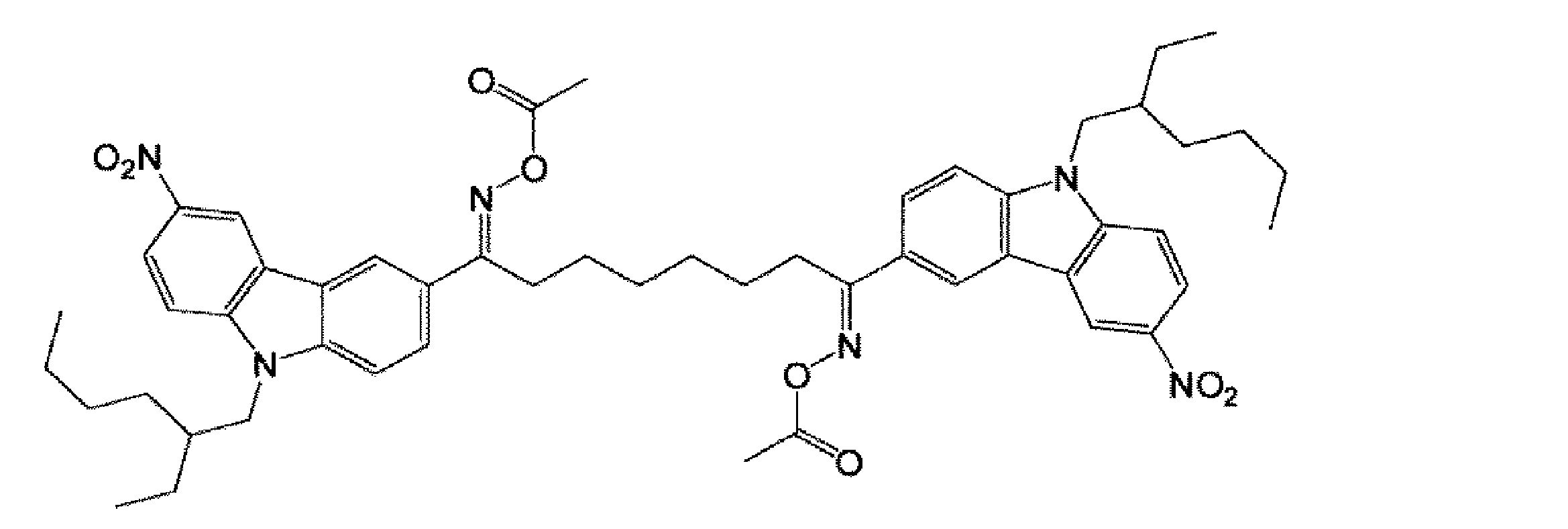
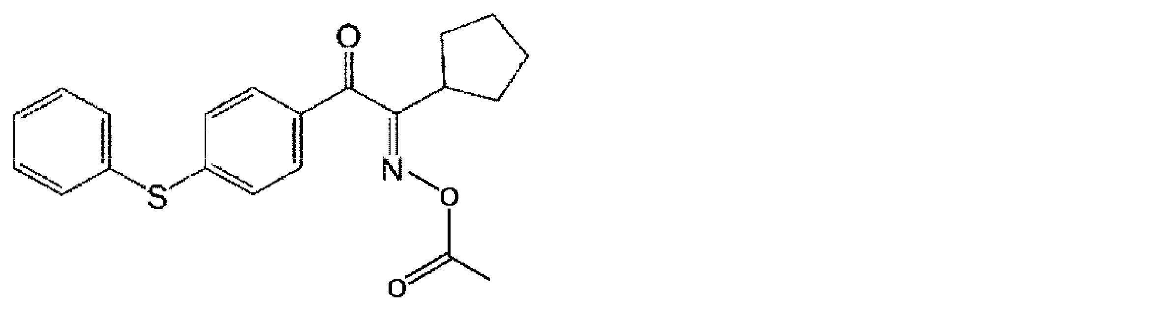
メチルエチルケトン:東燃化学合同会社製
Claims (8)
- 支持フィルムと、前記支持フィルム上に設けられた感光層と、を備え、
前記感光層が複数の導電性繊維を含み、
前記導電性繊維のそれぞれと、前記感光層における前記支持フィルム側の表面との間の最短距離の平均値が、0.1~50nmである、感光性導電フィルム。 - 前記導電性繊維が銀繊維である、請求項1に記載の感光性導電フィルム。
- 前記導電性繊維の繊維径が1~50nmである、請求項1又は2に記載の感光性導電フィルム。
- 前記導電性繊維の繊維長が1~100μmである、請求項1~3のいずれか一項に記載の感光性導電フィルム。
- 前記感光層が、エチレン性不飽和結合を有する光重合性化合物を含み、
前記光重合性化合物の水酸基価が90mgKOH/g以下である、請求項1~4のいずれか一項に記載の感光性導電フィルム。 - 前記感光層が、エチレン性不飽和結合を有する光重合性化合物を含み、
前記光重合性化合物の臨界表面張力が47mN/m以下である、請求項1~5のいずれか一項に記載の感光性導電フィルム。 - 前記感光層が、トリメチロールプロパントリ(メタ)アクリレート、エチレンオキサイド含有トリメチロールプロパントリ(メタ)アクリレート、プロピレンオキサイド含有トリメチロールプロパントリ(メタ)アクリレート、ジトリメチロールプロパンテトラ(メタ)アクリレート、及び、ジペンタエリスリトールヘキサ(メタ)アクリレートからなる群より選ばれる少なくとも一種を含む、請求項1~6のいずれか一項に記載の感光性導電フィルム。
- 前記感光層がトリメチロールプロパントリ(メタ)アクリレートを含む、請求項7に記載の感光性導電フィルム。
Priority Applications (3)
| Application Number | Priority Date | Filing Date | Title |
|---|---|---|---|
| KR1020167017577A KR20160133404A (ko) | 2014-03-14 | 2015-03-09 | 감광성 도전 필름 |
| JP2016507733A JP6547736B2 (ja) | 2014-03-14 | 2015-03-09 | 感光性導電フィルム |
| US15/125,879 US9709887B2 (en) | 2014-03-14 | 2015-03-09 | Photosensitive conductive film |
Applications Claiming Priority (2)
| Application Number | Priority Date | Filing Date | Title |
|---|---|---|---|
| JP2014-051702 | 2014-03-14 | ||
| JP2014051702 | 2014-03-14 |
Publications (1)
| Publication Number | Publication Date |
|---|---|
| WO2015137278A1 true WO2015137278A1 (ja) | 2015-09-17 |
Family
ID=54071722
Family Applications (1)
| Application Number | Title | Priority Date | Filing Date |
|---|---|---|---|
| PCT/JP2015/056832 WO2015137278A1 (ja) | 2014-03-14 | 2015-03-09 | 感光性導電フィルム |
Country Status (6)
| Country | Link |
|---|---|
| US (1) | US9709887B2 (ja) |
| JP (1) | JP6547736B2 (ja) |
| KR (1) | KR20160133404A (ja) |
| CN (1) | CN204790923U (ja) |
| TW (1) | TWI635423B (ja) |
| WO (1) | WO2015137278A1 (ja) |
Cited By (4)
| Publication number | Priority date | Publication date | Assignee | Title |
|---|---|---|---|---|
| JP2018040934A (ja) * | 2016-09-07 | 2018-03-15 | 日立化成株式会社 | 感光性導電フィルム、並びにこれを用いた導電パターン基板とその製造方法及びタッチパネルセンサ |
| JP2021047216A (ja) * | 2019-09-17 | 2021-03-25 | Jsr株式会社 | 硬化性組成物 |
| WO2021065322A1 (ja) * | 2019-09-30 | 2021-04-08 | 富士フイルム株式会社 | 転写フィルム、積層体の製造方法、積層体、タッチパネルセンサー、タッチパネル |
| JP7219378B1 (ja) | 2021-12-09 | 2023-02-08 | 東洋インキScホールディングス株式会社 | 感光性着色組成物、光学フィルタ、画像表示装置、及び固体撮像素子 |
Families Citing this family (1)
| Publication number | Priority date | Publication date | Assignee | Title |
|---|---|---|---|---|
| CN107168593B (zh) * | 2017-05-10 | 2020-01-14 | 京东方科技集团股份有限公司 | 一种触控电极及触控电极制作方法 |
Citations (4)
| Publication number | Priority date | Publication date | Assignee | Title |
|---|---|---|---|---|
| JP2008126469A (ja) * | 2006-11-20 | 2008-06-05 | Takiron Co Ltd | 導電性樹脂成形体及びその製造方法 |
| JP2009505358A (ja) * | 2005-08-12 | 2009-02-05 | カンブリオス テクノロジーズ コーポレイション | ナノワイヤに基づく透明導電体 |
| WO2012133367A1 (ja) * | 2011-03-28 | 2012-10-04 | 東レ株式会社 | 導電積層体およびタッチパネル |
| WO2013051516A1 (ja) * | 2011-10-03 | 2013-04-11 | 日立化成株式会社 | 導電パターンの形成方法、導電パターン基板及びタッチパネルセンサ |
Family Cites Families (7)
| Publication number | Priority date | Publication date | Assignee | Title |
|---|---|---|---|---|
| JP2010021224A (ja) | 2008-07-09 | 2010-01-28 | Shimadzu Corp | レーザ装置 |
| KR20150061016A (ko) | 2008-08-22 | 2015-06-03 | 히타치가세이가부시끼가이샤 | 감광성 도전 필름, 도전막의 형성 방법, 도전 패턴의 형성 방법 및 도전막 기판 |
| JP5472290B2 (ja) * | 2009-03-17 | 2014-04-16 | コニカミノルタ株式会社 | 透明導電膜の製造方法 |
| JP2011018636A (ja) * | 2009-06-09 | 2011-01-27 | Fujifilm Corp | 導電性組成物、並びに透明導電膜、表示素子及び集積型太陽電池 |
| JP2012169072A (ja) * | 2011-02-10 | 2012-09-06 | Fujifilm Corp | 導電膜形成用積層体、導電膜形成方法、導電膜、導電要素、タッチパネル及び集積型太陽電池 |
| CN103503081B (zh) * | 2011-04-28 | 2016-11-23 | 富士胶片株式会社 | 导电性构件、其制造方法、触摸屏及太阳电池 |
| JP2013051516A (ja) | 2011-08-30 | 2013-03-14 | Aof Imaging Technology Ltd | 撮像装置および判定方法、並びにプログラム |
-
2015
- 2015-03-09 KR KR1020167017577A patent/KR20160133404A/ko not_active Withdrawn
- 2015-03-09 US US15/125,879 patent/US9709887B2/en active Active
- 2015-03-09 WO PCT/JP2015/056832 patent/WO2015137278A1/ja active Application Filing
- 2015-03-09 JP JP2016507733A patent/JP6547736B2/ja not_active Expired - Fee Related
- 2015-03-13 CN CN201520146246.XU patent/CN204790923U/zh not_active Expired - Fee Related
- 2015-03-13 TW TW104108005A patent/TWI635423B/zh not_active IP Right Cessation
Patent Citations (4)
| Publication number | Priority date | Publication date | Assignee | Title |
|---|---|---|---|---|
| JP2009505358A (ja) * | 2005-08-12 | 2009-02-05 | カンブリオス テクノロジーズ コーポレイション | ナノワイヤに基づく透明導電体 |
| JP2008126469A (ja) * | 2006-11-20 | 2008-06-05 | Takiron Co Ltd | 導電性樹脂成形体及びその製造方法 |
| WO2012133367A1 (ja) * | 2011-03-28 | 2012-10-04 | 東レ株式会社 | 導電積層体およびタッチパネル |
| WO2013051516A1 (ja) * | 2011-10-03 | 2013-04-11 | 日立化成株式会社 | 導電パターンの形成方法、導電パターン基板及びタッチパネルセンサ |
Cited By (8)
| Publication number | Priority date | Publication date | Assignee | Title |
|---|---|---|---|---|
| JP2018040934A (ja) * | 2016-09-07 | 2018-03-15 | 日立化成株式会社 | 感光性導電フィルム、並びにこれを用いた導電パターン基板とその製造方法及びタッチパネルセンサ |
| JP2021047216A (ja) * | 2019-09-17 | 2021-03-25 | Jsr株式会社 | 硬化性組成物 |
| KR20210032914A (ko) * | 2019-09-17 | 2021-03-25 | 제이에스알 가부시끼가이샤 | 경화성 조성물 |
| JP7570169B2 (ja) | 2019-09-17 | 2024-10-21 | Jsr株式会社 | 硬化性組成物 |
| KR102775707B1 (ko) | 2019-09-17 | 2025-04-28 | 제이에스알 가부시키가이샤 | 경화성 조성물 |
| WO2021065322A1 (ja) * | 2019-09-30 | 2021-04-08 | 富士フイルム株式会社 | 転写フィルム、積層体の製造方法、積層体、タッチパネルセンサー、タッチパネル |
| JP7219378B1 (ja) | 2021-12-09 | 2023-02-08 | 東洋インキScホールディングス株式会社 | 感光性着色組成物、光学フィルタ、画像表示装置、及び固体撮像素子 |
| JP2023085600A (ja) * | 2021-12-09 | 2023-06-21 | 東洋インキScホールディングス株式会社 | 感光性着色組成物、光学フィルタ、画像表示装置、及び固体撮像素子 |
Also Published As
| Publication number | Publication date |
|---|---|
| US9709887B2 (en) | 2017-07-18 |
| CN204790923U (zh) | 2015-11-18 |
| US20170003588A1 (en) | 2017-01-05 |
| TW201602864A (zh) | 2016-01-16 |
| KR20160133404A (ko) | 2016-11-22 |
| TWI635423B (zh) | 2018-09-11 |
| JP6547736B2 (ja) | 2019-07-24 |
| JPWO2015137278A1 (ja) | 2017-04-06 |
Similar Documents
| Publication | Publication Date | Title |
|---|---|---|
| JP5858190B2 (ja) | 金属繊維の劣化抑制方法、膜、及び膜の製造方法 | |
| JP6400289B2 (ja) | 硬化膜付きタッチパネル用基材及びその製造方法、感光性エレメント並びにタッチパネル | |
| JP6547736B2 (ja) | 感光性導電フィルム | |
| WO2016167228A1 (ja) | 感光性導電フィルム、導電パターンの形成方法、導電パターン付き基材、及びタッチパネルセンサ | |
| JP6206028B2 (ja) | 導電パターンの製造方法、その方法により製造された導電パターンを備える導電パターン基板、その導電パターン基板を含むタッチパネルセンサ、及び感光性導電フィルム | |
| JP6551277B2 (ja) | 硬化膜付きタッチパネル用基材の製造方法、それに用いる感光性樹脂組成物、感光性エレメント及びタッチパネル | |
| JP6205925B2 (ja) | 感光性導電フィルム、並びにこれを用いた導電パターンの形成方法及び導電パターン基板 | |
| JP2015172674A (ja) | 感光性樹脂組成物、感光性エレメント、硬化膜付き透明基板の製造方法及び硬化膜付き透明基板 | |
| JP6399175B2 (ja) | 導電パターンの製造方法、その方法により製造された導電パターンを備える導電パターン基板、その導電パターン基板を含むタッチパネルセンサ、及び感光性導電フィルム | |
| JP2016151748A (ja) | 感光性導電フィルム、それを用いた導電パターンの形成方法、導電パターン基板及びタッチパネルセンサ | |
| JP2017198878A (ja) | 感光性導電フィルム及びそれを用いた導電パターン、導電パターン基板、タッチパネルセンサの製造方法 | |
| WO2014196154A1 (ja) | 感光性導電フィルム、並びにこれを用いた導電パターンの形成方法及び導電パターン基板 | |
| JP2019179109A (ja) | 感光性導電フィルム及びその製造方法、導電パターンの形成方法、導電パターン基材、並びにタッチパネルセンサ | |
| WO2016013587A1 (ja) | 感光性樹脂組成物、感光性フィルム、パターン基板、感光性導電フィルム及び導電パターン基板 | |
| WO2018008599A1 (ja) | 感光性導電フィルム、導電パターンの製造方法、導電パターン基板及びタッチパネルセンサ | |
| JP2017072679A (ja) | 感光性導電フィルム、導電パターンの形成方法 | |
| JP2017068158A (ja) | 感光性導電フィルム、それを用いる導電パターンの形成方法 | |
| JP2017068734A (ja) | 感光性導電フィルム、それを用いる導電パターンの形成方法 | |
| JP2018139076A (ja) | 感光性導電フィルム及びその製造方法、導電パターンの製造方法、導電パターン基材、並びにタッチパネルセンサ | |
| JP2021144723A (ja) | 硬化膜付きタッチパネル用基材の製造方法、それに用いる感光性樹脂組成物、感光性エレメント及びタッチパネル | |
| TW201830143A (zh) | 感光性樹脂組成物、感光性元件、保護膜及觸控面板 | |
| WO2018087816A1 (ja) | 感光性導電フィルム、導電パターンの形成方法及び導電パターン基材の製造方法 | |
| JP2018040934A (ja) | 感光性導電フィルム、並びにこれを用いた導電パターン基板とその製造方法及びタッチパネルセンサ | |
| JP2018097576A (ja) | 接続用配線及び接続用配線の形成方法 | |
| WO2016181496A1 (ja) | 導電膜作製液セット、導電パターンの形成方法、及びタッチパネル |
Legal Events
| Date | Code | Title | Description |
|---|---|---|---|
| 121 | Ep: the epo has been informed by wipo that ep was designated in this application |
Ref document number: 15762450 Country of ref document: EP Kind code of ref document: A1 |
|
| ENP | Entry into the national phase |
Ref document number: 2016507733 Country of ref document: JP Kind code of ref document: A |
|
| ENP | Entry into the national phase |
Ref document number: 20167017577 Country of ref document: KR Kind code of ref document: A |
|
| WWE | Wipo information: entry into national phase |
Ref document number: 15125879 Country of ref document: US |
|
| NENP | Non-entry into the national phase |
Ref country code: DE |
|
| 122 | Ep: pct application non-entry in european phase |
Ref document number: 15762450 Country of ref document: EP Kind code of ref document: A1 |