WO2015136589A1 - 表示パネルの製造方法 - Google Patents
表示パネルの製造方法 Download PDFInfo
- Publication number
- WO2015136589A1 WO2015136589A1 PCT/JP2014/006441 JP2014006441W WO2015136589A1 WO 2015136589 A1 WO2015136589 A1 WO 2015136589A1 JP 2014006441 W JP2014006441 W JP 2014006441W WO 2015136589 A1 WO2015136589 A1 WO 2015136589A1
- Authority
- WO
- WIPO (PCT)
- Prior art keywords
- line
- display
- lighting
- pixel
- display panel
- Prior art date
- Legal status (The legal status is an assumption and is not a legal conclusion. Google has not performed a legal analysis and makes no representation as to the accuracy of the status listed.)
- Ceased
Links
Images





Classifications
-
- G—PHYSICS
- G01—MEASURING; TESTING
- G01R—MEASURING ELECTRIC VARIABLES; MEASURING MAGNETIC VARIABLES
- G01R31/00—Arrangements for testing electric properties; Arrangements for locating electric faults; Arrangements for electrical testing characterised by what is being tested not provided for elsewhere
- G01R31/50—Testing of electric apparatus, lines, cables or components for short-circuits, continuity, leakage current or incorrect line connections
- G01R31/58—Testing of lines, cables or conductors
- G01R31/59—Testing of lines, cables or conductors while the cable continuously passes the testing apparatus, e.g. during manufacture
-
- G—PHYSICS
- G01—MEASURING; TESTING
- G01M—TESTING STATIC OR DYNAMIC BALANCE OF MACHINES OR STRUCTURES; TESTING OF STRUCTURES OR APPARATUS, NOT OTHERWISE PROVIDED FOR
- G01M11/00—Testing of optical apparatus; Testing structures by optical methods not otherwise provided for
- G01M11/02—Testing optical properties
- G01M11/0242—Testing optical properties by measuring geometrical properties or aberrations
- G01M11/0257—Testing optical properties by measuring geometrical properties or aberrations by analyzing the image formed by the object to be tested
-
- G—PHYSICS
- G01—MEASURING; TESTING
- G01M—TESTING STATIC OR DYNAMIC BALANCE OF MACHINES OR STRUCTURES; TESTING OF STRUCTURES OR APPARATUS, NOT OTHERWISE PROVIDED FOR
- G01M11/00—Testing of optical apparatus; Testing structures by optical methods not otherwise provided for
- G01M11/02—Testing optical properties
- G01M11/0242—Testing optical properties by measuring geometrical properties or aberrations
- G01M11/0257—Testing optical properties by measuring geometrical properties or aberrations by analyzing the image formed by the object to be tested
- G01M11/0264—Testing optical properties by measuring geometrical properties or aberrations by analyzing the image formed by the object to be tested by using targets or reference patterns
-
- G—PHYSICS
- G01—MEASURING; TESTING
- G01R—MEASURING ELECTRIC VARIABLES; MEASURING MAGNETIC VARIABLES
- G01R31/00—Arrangements for testing electric properties; Arrangements for locating electric faults; Arrangements for electrical testing characterised by what is being tested not provided for elsewhere
- G01R31/26—Testing of individual semiconductor devices
-
- G—PHYSICS
- G09—EDUCATION; CRYPTOGRAPHY; DISPLAY; ADVERTISING; SEALS
- G09G—ARRANGEMENTS OR CIRCUITS FOR CONTROL OF INDICATING DEVICES USING STATIC MEANS TO PRESENT VARIABLE INFORMATION
- G09G3/00—Control arrangements or circuits, of interest only in connection with visual indicators other than cathode-ray tubes
- G09G3/006—Electronic inspection or testing of displays and display drivers, e.g. of LED or LCD displays
-
- G—PHYSICS
- G09—EDUCATION; CRYPTOGRAPHY; DISPLAY; ADVERTISING; SEALS
- G09G—ARRANGEMENTS OR CIRCUITS FOR CONTROL OF INDICATING DEVICES USING STATIC MEANS TO PRESENT VARIABLE INFORMATION
- G09G3/00—Control arrangements or circuits, of interest only in connection with visual indicators other than cathode-ray tubes
- G09G3/20—Control arrangements or circuits, of interest only in connection with visual indicators other than cathode-ray tubes for presentation of an assembly of a number of characters, e.g. a page, by composing the assembly by combination of individual elements arranged in a matrix no fixed position being assigned to or needed to be assigned to the individual characters or partial characters
- G09G3/22—Control arrangements or circuits, of interest only in connection with visual indicators other than cathode-ray tubes for presentation of an assembly of a number of characters, e.g. a page, by composing the assembly by combination of individual elements arranged in a matrix no fixed position being assigned to or needed to be assigned to the individual characters or partial characters using controlled light sources
- G09G3/30—Control arrangements or circuits, of interest only in connection with visual indicators other than cathode-ray tubes for presentation of an assembly of a number of characters, e.g. a page, by composing the assembly by combination of individual elements arranged in a matrix no fixed position being assigned to or needed to be assigned to the individual characters or partial characters using controlled light sources using electroluminescent panels
- G09G3/32—Control arrangements or circuits, of interest only in connection with visual indicators other than cathode-ray tubes for presentation of an assembly of a number of characters, e.g. a page, by composing the assembly by combination of individual elements arranged in a matrix no fixed position being assigned to or needed to be assigned to the individual characters or partial characters using controlled light sources using electroluminescent panels semiconductive, e.g. using light-emitting diodes [LED]
- G09G3/3208—Control arrangements or circuits, of interest only in connection with visual indicators other than cathode-ray tubes for presentation of an assembly of a number of characters, e.g. a page, by composing the assembly by combination of individual elements arranged in a matrix no fixed position being assigned to or needed to be assigned to the individual characters or partial characters using controlled light sources using electroluminescent panels semiconductive, e.g. using light-emitting diodes [LED] organic, e.g. using organic light-emitting diodes [OLED]
- G09G3/3225—Control arrangements or circuits, of interest only in connection with visual indicators other than cathode-ray tubes for presentation of an assembly of a number of characters, e.g. a page, by composing the assembly by combination of individual elements arranged in a matrix no fixed position being assigned to or needed to be assigned to the individual characters or partial characters using controlled light sources using electroluminescent panels semiconductive, e.g. using light-emitting diodes [LED] organic, e.g. using organic light-emitting diodes [OLED] using an active matrix
- G09G3/3233—Control arrangements or circuits, of interest only in connection with visual indicators other than cathode-ray tubes for presentation of an assembly of a number of characters, e.g. a page, by composing the assembly by combination of individual elements arranged in a matrix no fixed position being assigned to or needed to be assigned to the individual characters or partial characters using controlled light sources using electroluminescent panels semiconductive, e.g. using light-emitting diodes [LED] organic, e.g. using organic light-emitting diodes [OLED] using an active matrix with pixel circuitry controlling the current through the light-emitting element
-
- G—PHYSICS
- G01—MEASURING; TESTING
- G01R—MEASURING ELECTRIC VARIABLES; MEASURING MAGNETIC VARIABLES
- G01R31/00—Arrangements for testing electric properties; Arrangements for locating electric faults; Arrangements for electrical testing characterised by what is being tested not provided for elsewhere
- G01R31/26—Testing of individual semiconductor devices
- G01R31/2607—Circuits therefor
- G01R31/2632—Circuits therefor for testing diodes
- G01R31/2635—Testing light-emitting diodes, laser diodes or photodiodes
-
- G—PHYSICS
- G01—MEASURING; TESTING
- G01R—MEASURING ELECTRIC VARIABLES; MEASURING MAGNETIC VARIABLES
- G01R31/00—Arrangements for testing electric properties; Arrangements for locating electric faults; Arrangements for electrical testing characterised by what is being tested not provided for elsewhere
- G01R31/26—Testing of individual semiconductor devices
- G01R31/2607—Circuits therefor
- G01R31/2637—Circuits therefor for testing other individual devices
- G01R31/2639—Circuits therefor for testing other individual devices for testing field-effect devices, e.g. of MOS-capacitors
-
- G—PHYSICS
- G09—EDUCATION; CRYPTOGRAPHY; DISPLAY; ADVERTISING; SEALS
- G09G—ARRANGEMENTS OR CIRCUITS FOR CONTROL OF INDICATING DEVICES USING STATIC MEANS TO PRESENT VARIABLE INFORMATION
- G09G2300/00—Aspects of the constitution of display devices
- G09G2300/08—Active matrix structure, i.e. with use of active elements, inclusive of non-linear two terminal elements, in the pixels together with light emitting or modulating elements
- G09G2300/0809—Several active elements per pixel in active matrix panels
- G09G2300/0819—Several active elements per pixel in active matrix panels used for counteracting undesired variations, e.g. feedback or autozeroing
-
- G—PHYSICS
- G09—EDUCATION; CRYPTOGRAPHY; DISPLAY; ADVERTISING; SEALS
- G09G—ARRANGEMENTS OR CIRCUITS FOR CONTROL OF INDICATING DEVICES USING STATIC MEANS TO PRESENT VARIABLE INFORMATION
- G09G2300/00—Aspects of the constitution of display devices
- G09G2300/08—Active matrix structure, i.e. with use of active elements, inclusive of non-linear two terminal elements, in the pixels together with light emitting or modulating elements
- G09G2300/0809—Several active elements per pixel in active matrix panels
- G09G2300/0842—Several active elements per pixel in active matrix panels forming a memory circuit, e.g. a dynamic memory with one capacitor
-
- G—PHYSICS
- G09—EDUCATION; CRYPTOGRAPHY; DISPLAY; ADVERTISING; SEALS
- G09G—ARRANGEMENTS OR CIRCUITS FOR CONTROL OF INDICATING DEVICES USING STATIC MEANS TO PRESENT VARIABLE INFORMATION
- G09G2310/00—Command of the display device
- G09G2310/02—Addressing, scanning or driving the display screen or processing steps related thereto
- G09G2310/0243—Details of the generation of driving signals
- G09G2310/0254—Control of polarity reversal in general, other than for liquid crystal displays
- G09G2310/0256—Control of polarity reversal in general, other than for liquid crystal displays with the purpose of reversing the voltage across a light emitting or modulating element within a pixel
-
- G—PHYSICS
- G09—EDUCATION; CRYPTOGRAPHY; DISPLAY; ADVERTISING; SEALS
- G09G—ARRANGEMENTS OR CIRCUITS FOR CONTROL OF INDICATING DEVICES USING STATIC MEANS TO PRESENT VARIABLE INFORMATION
- G09G2310/00—Command of the display device
- G09G2310/02—Addressing, scanning or driving the display screen or processing steps related thereto
- G09G2310/0262—The addressing of the pixel, in a display other than an active matrix LCD, involving the control of two or more scan electrodes or two or more data electrodes, e.g. pixel voltage dependent on signals of two data electrodes
-
- G—PHYSICS
- G09—EDUCATION; CRYPTOGRAPHY; DISPLAY; ADVERTISING; SEALS
- G09G—ARRANGEMENTS OR CIRCUITS FOR CONTROL OF INDICATING DEVICES USING STATIC MEANS TO PRESENT VARIABLE INFORMATION
- G09G2320/00—Control of display operating conditions
- G09G2320/02—Improving the quality of display appearance
- G09G2320/0233—Improving the luminance or brightness uniformity across the screen
-
- G—PHYSICS
- G09—EDUCATION; CRYPTOGRAPHY; DISPLAY; ADVERTISING; SEALS
- G09G—ARRANGEMENTS OR CIRCUITS FOR CONTROL OF INDICATING DEVICES USING STATIC MEANS TO PRESENT VARIABLE INFORMATION
- G09G2330/00—Aspects of power supply; Aspects of display protection and defect management
- G09G2330/10—Dealing with defective pixels
-
- G—PHYSICS
- G09—EDUCATION; CRYPTOGRAPHY; DISPLAY; ADVERTISING; SEALS
- G09G—ARRANGEMENTS OR CIRCUITS FOR CONTROL OF INDICATING DEVICES USING STATIC MEANS TO PRESENT VARIABLE INFORMATION
- G09G3/00—Control arrangements or circuits, of interest only in connection with visual indicators other than cathode-ray tubes
- G09G3/20—Control arrangements or circuits, of interest only in connection with visual indicators other than cathode-ray tubes for presentation of an assembly of a number of characters, e.g. a page, by composing the assembly by combination of individual elements arranged in a matrix no fixed position being assigned to or needed to be assigned to the individual characters or partial characters
- G09G3/2003—Display of colours
Definitions
- the present disclosure relates to a method for manufacturing a display panel.
- a thin film transistor In an active matrix type organic EL display, a thin film transistor (TFT) is provided at an intersection of a plurality of scanning lines and a plurality of data lines, and a capacitor element and a gate of a driving transistor are connected to the TFT. Then, the TFT is turned on through the selected scanning line, a data signal from the data line is input to the driving transistor and the capacitor element, and the light emission timing of the organic EL element is controlled by the driving transistor and the capacitor element.
- a pixel circuit composed of a TFT, a capacitor element, a drive transistor, and an organic EL element becomes more complicated, and as the number of light emitting pixels increases, circuit elements and Electrical problems such as short-circuiting and opening of wiring will occur.
- Patent Document 1 in order to correct a defective pixel that is always in a light-emitting state due to a short circuit of a circuit element or the like and becomes a bright spot, all pixels have non-overlapping portions connected apart from other conductive portions and wirings. Is provided. By irradiating the non-overlapping portion of the defective pixel with a laser, the non-overlapping portion is cut. As a result, the defective pixel is blocked from transmission of electrical signals, and is darkened without being damaged by laser irradiation.
- a bright spot pixel in black display or a dark spot pixel in white display must be specified as a stage before repairing a defective pixel by irradiating a laser.
- the defect may be observed as a line (pixel row or pixel column) defect rather than a point (pixel) defect.
- the defect may be observed as a line (pixel row or pixel column) defect rather than a point (pixel) defect.
- the present disclosure provides a method for manufacturing a display panel in which a defective pixel inspection process is simplified and shortened.
- a method for manufacturing a display panel includes a light-emitting element and a drive element that drives the light-emitting element, and emits light with luminance that reflects an input display gradation signal.
- a display panel having a display unit in which a plurality of pixels to be arranged are arranged in a matrix, wherein the line defect is at least one of a predetermined pixel row and a pixel column that emits light at a luminance that does not reflect the display gradation signal
- a lighting line which is a pixel row or a pixel column emitted by inputting a uniform display gradation signal is displayed on the display unit, and the lighting line is displayed in a row direction or a column direction in the display unit.
- the inspection process for a display panel having a line defect can be simplified and shortened.
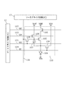
- FIG. 1 is a schematic configuration diagram of a display panel according to an embodiment.
- FIG. 2 is a circuit configuration diagram illustrating an example of a pixel circuit according to the embodiment.
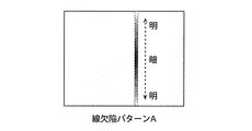
- FIG. 3A is an image diagram of the display unit when the line defect pattern A appears.
- FIG. 3B is an image diagram of the display unit when the line defect pattern B appears.
- FIG. 4 is an operation flowchart illustrating a method for manufacturing the display panel according to the embodiment.
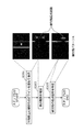
- FIG. 5A is an operation flowchart for explaining the defective pixel specifying step according to the embodiment when the line defect pattern A appears.
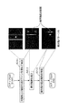
- FIG. 5B is an operation flowchart for explaining the defective pixel specifying step according to the embodiment when the line defect pattern B appears.
- FIG. 5A is an operation flowchart for explaining the defective pixel specifying step according to the embodiment when the line defect pattern A appears.
- FIG. 5B is an operation flowchart for explaining the defective pixel specifying step according to the embodiment when the line defect pattern B appears.
- FIG. 5A is
- FIG. 6 is an operation flowchart illustrating a method for manufacturing a display panel according to the first modification of the embodiment.
- FIG. 7 is a schematic configuration diagram of a display panel according to Modification 2 of the embodiment.
- FIG. 8 is an external view of a thin flat TV manufactured by using the display panel manufacturing method according to the embodiment.
- FIG. 1 is a schematic configuration diagram of a display panel according to an embodiment.
- the display panel 1 according to the present embodiment includes a display unit 11, gate signal lines 121 to 124, a source signal line 131, a gate driver circuit 12, and a source driver circuit 13. .
- the display unit 11 includes pixels 110 arranged in a matrix and displays an image based on a video signal input from the outside.
- the gate signal lines 121 to 124 are scanning lines that are arranged for each pixel row of the display unit 11 and transmit a control signal for switching between conduction and non-conduction of a switch included in the pixel 110.
- the gate signal lines 121 to 124 are connected to the gate driver circuit 12 and are connected to the pixels 110 belonging to each pixel row.
- the source signal line 131 is a data line that is arranged for each pixel column of the display unit 11 and transmits a data voltage, which is a display gradation signal reflecting an externally input video signal, to the pixel 110.
- the gate driver circuit 12 is a peripheral circuit of the display unit 11, and outputs the control signal to the gate signal lines 121 to 124.
- the gate driver circuit 12 has a function of controlling the timing of writing a data voltage to the pixel 110, a function of controlling the timing of applying various voltages such as an initialization voltage and a reference voltage to the pixel 110, and the like.
- the source driver circuit 13 is a peripheral circuit of the display unit 11 and outputs a data voltage to the source signal line 131.
- FIG. 2 is a circuit configuration diagram illustrating an example of a pixel circuit according to the embodiment.
- a circuit configuration of one pixel 110 of the plurality of pixels 110 included in the display unit 11 and a connection configuration between the pixel 110 and a peripheral circuit are illustrated.
- the pixel 110 includes an organic EL element 101, a drive transistor 102, switches 103-106, and a capacitor element 107.
- the organic EL element 101 is an example of a light emitting element, and emits light by the driving current of the driving transistor 102.
- an EL cathode voltage Vss is applied to the cathode, and the source of the driving transistor 102 is connected to the anode.
- the drive transistor 102 is a voltage-driven drive element that controls the supply of current to the organic EL element 101.
- the driving transistor 102 has a gate connected to the first electrode of the capacitor 107 and a source connected to the second electrode of the capacitor 107 and the anode of the organic EL element 101.
- the drive transistor 102 causes the organic EL element 101 to emit light by flowing a drive current that is a current corresponding to the data voltage corresponding to the display gradation to the organic EL element 101.
- the threshold voltage of the driving transistor 102 is detected by the capacitor 107 while the switch 106 is on, the switch 103 is off, the switch 104 is off, and the switch 105 is on.
- the capacitor element 107 holds a voltage that determines the amount of current flowing through the driving transistor 102.
- a first electrode of the capacitor 107 is connected to the gate of the driving transistor 102, and a reference voltage Vref is applied via the switch 106.
- the capacitive element 107 maintains the applied reference voltage Vref even after the switch 106 is turned off, and continuously supplies the reference voltage Vref to the gate of the driving transistor 102.
- the capacitor 107 is applied with a data voltage when the switch 103 is turned on, and retains the data voltage after the switch 106 is turned off. Then, a drive current is supplied to the drive transistor 102 after the switch 105 is turned on.
- the switch 103 is a switching NMOS transistor having a gate electrically connected to the gate signal line 121, a source electrically connected to the gate of the driving transistor 102, and a drain electrically connected to the source signal line 131. . With the above connection configuration, the switch 103 switches between conduction and non-conduction between the source signal line 131 for supplying the data voltage and the first electrode of the capacitor 107.
- the switch 106 is a switching NMOS transistor in which the gate is electrically connected to the gate signal line 123, the source is electrically connected to the gate of the driving transistor 102, and the reference voltage Vref is applied to the drain.
- the switch 106 switches between applying and not applying the reference voltage Vref to the first electrode of the capacitor 107.
- the switch 104 is a switching NMOS transistor whose gate is electrically connected to the gate signal line 124, whose source is electrically connected to the source of the driving transistor 102, and whose initialization voltage Vini is applied to the drain.
- the switch 104 switches between applying and not applying the initialization voltage Vini to the second electrode of the capacitor 107.
- the switch 105 is a switching NMOS transistor having a gate electrically connected to the gate signal line 122, a source electrically connected to the drain of the driving transistor 102, and an EL anode power supply voltage Vdd being applied to the drain.
- the EL anode power supply voltage Vdd is a drive power supply voltage that drives the drive transistor 102.
- the switch 105 switches between applying and not applying the EL anode power supply voltage Vdd to the drain of the driving transistor 102.
- the switch 105 has a function of applying a potential Vdd to the drain of the driving transistor 102 and a function of detecting the threshold voltage Vth of the driving transistor 102.
- switches 103 to 106 are described as n-type TFTs, they may be p-type TFTs or a mixture of n-type TFTs and p-type TFTs.
- FIG. 3A is an image diagram of the display unit when the line defect pattern A appears
- FIG. 3B is an image diagram of the display unit when the line defect pattern B appears.
- the images shown in FIGS. 3A and 3B are images when a data voltage for a uniform display gradation is supplied from the source driver circuit 13 to all the pixels 110 of the display unit 11.
- the vertical streak line defect is visible.
- This vertical stripe-like line defect is composed of a predetermined pixel row that emits light at a luminance that does not reflect the data voltage that is the input display gradation signal. More specifically, in the image of FIG. 3A, the display portion 11 changes stepwise from light to dark as it goes from the upper and lower ends to the center. On the other hand, in the image of FIG. 3B, as it goes from the upper and lower end portions of the display unit 11 toward the center, it gradually changes from dark to bright.
- a short circuit failure of a switch constituting the pixel circuit can be cited.
- the drain and gate of the switch 103 of one pixel 110 included in the display unit 11 are short-circuited.
- the control voltage GS applied from the gate driver circuit 12 to the gate of the switch 103 via the gate signal line 121 and the data voltage Vdata applied from the source driver circuit 13 to the drain of the switch 103 via the data line are: , Different voltage values are set.
- the voltage of the source signal line 131 is output from the source driver circuit 13 under the influence of the voltage of the gate signal line 121 control voltage GS. It fluctuates from the voltage value of the data voltage Vdata.
- the source signal line 131 that has received this potential variation is arranged in the pixel column to which the pixel 110 (hereinafter referred to as a defective pixel) in which the drain and gate of the switch 103 are short-circuited belongs. Therefore, the pixels 110 belonging to the pixel column are supplied with a data voltage that does not reflect the input display gradation signal from the source signal line 131 that has received the potential fluctuation.
- the source signal line 131 since the source signal line 131 has a predetermined wiring resistance, in the source signal line 131 that has undergone potential fluctuation, the potential fluctuation becomes more severe as it is closer to the defective pixel. Therefore, a pixel that belongs to the same pixel column as the defective pixel and is closer to the defective pixel emits light with a luminance closer to the emission luminance of the defective pixel, and a pixel that belongs to the same pixel column as the defective pixel and is farther from the defective pixel Light is emitted at a luminance different from the emission luminance.
- the control voltage GS is set to a voltage value of 0 V or less.
- the potential of the source signal line 131 fluctuates in a decreasing direction.
- the pixel 110 belonging to the same pixel column and close to the defective pixel emits light with a luminance lower than the luminance to be originally displayed, and the line defect pattern A appears.
- the control voltage GS is set to a voltage value of 0 V or less.
- the potential of the source signal line 131 fluctuates in a decreasing direction.
- the pixel 110 belonging to the same pixel column and close to the defective pixel emits light with a luminance higher than the luminance to be originally displayed, and the line defect pattern B appears.
- the above-described line defects are not only vertical streak line defects due to potential fluctuations of the source signal line 131 but also horizontal streak lines generated by a short circuit between the gate and drain of the switch 104-106 and between the gate and source. Defects are also included.
- the source signal line 131 is required to supply the data voltage to the pixel 110 at a high speed, the source signal line 131 is set to have a lower impedance than the gate signal lines 121-124. For this reason, the source signal line 131 is more susceptible to potential fluctuations than the gate signal lines 121 to 124, and vertical line-like line defects appear more remarkably than horizontal lines.
- the defective pixel can be specified by the display panel manufacturing method according to the present embodiment.
- FIG. 4 is an operation flowchart illustrating a method for manufacturing the display panel according to the embodiment.
- the display panel manufacturing method of the present disclosure includes a display panel formation process, a defective pixel identification process, and a repair process.
- a display panel is formed on a display panel substrate (S10). Specifically, for example, a drive circuit layer in which the drive transistor 102, the switches 103-106, the capacitor 107, the gate signal lines 121 to 124, the source signal line 131, and the like shown in FIG. .
- a light emitting layer having the organic EL element 101 is formed on the drive circuit layer after a flattening process of the drive circuit layer.
- the light emitting layer includes, for example, an anode, a hole injection layer, a hole transport layer, an organic light emitting layer, a bank layer, an electron injection layer, and a transparent cathode.
- step S20 that is a main part of the method for manufacturing a display panel according to the present disclosure will be described in detail.
- the vertical streak-like line defect pattern A that changes from bright to dark and bright to the lower end from the upper end of the display unit 11, and dark, bright and dark from the upper end to the lower end of the display unit 11
- the defective pixel specifying step of the vertical line-shaped line defect pattern B that changes to dark will be described in order.
- FIG. 5A is an operation flowchart for explaining the defective pixel specifying step according to the embodiment when the line defect pattern A appears.
- a linear lighting line is superimposed on the defect line and displayed (S201).
- the display unit 11 displays a lighting line that is a pixel column to which a uniform display gradation signal is input from the source driver circuit 13.
- the lighting line is scanned in the row direction (column scanning direction, left-right direction of the display unit) in the display unit 11, and the lighting line and the line defect are overlapped and displayed.
- it is desirable that the pixels not belonging to the lighting line are turned off uniformly. Thereby, the contrast between the lighting line and other pixels is improved, and the visibility of the lighting line can be increased.
- step S201 as a specific method for displaying the lighting line, the gate driver circuit 12 is supplied with the control voltages GS, GE, GR, and GI of the HIGH level to the gate signal lines 121 to 124 in the row order.
- the source driver circuit 13 is supplied with a data voltage, which is a display gradation signal for uniformly lighting the pixel column, only to the source signal line 131 arranged in the predetermined pixel column.
- the source signal line 131 that supplies the data voltage is scanned in the column order in the source driver circuit 13.
- the observer stops the column scanning of the lighting line when the lighting line shifted in the column order overlaps the pixel column having the line defect observed in advance.
- the display gradation of the lighting line is increased (S203).
- the source driver circuit 13 is applied to the source signal line 131 arranged in the pixel column to which the defective pixel belongs, in which the lighting line is overlapped.
- the data voltage is changed so that the display gradation of the lighting line becomes higher.
- the light emission luminance of the organic EL element 101 in the pixel column to which the defective pixel belongs increases, so that the dark part range of the line defect can be reduced.
- step S203 the EL anode power supply voltage Vdd may be increased instead of changing the data voltage as a method for increasing the display gradation of the lighting line overlapped with the line defect.
- the light emission current flowing through the organic EL element 101 in the pixel column to which the defective pixel belongs increases, and the light emission luminance of the organic EL element 101 increases, so that the dark defect range of the line defect can be reduced.
- the starting point of the line defect is specified (S205). Specifically, the defective pixel that is the starting point of the line defect is specified from the position in the display unit 11 of the dark range reduced in step S203.
- step S203 it can be determined in step S203 that a defective pixel is included in a portion that remains as a dark portion even though the display gradation of the line defect is uniformly increased in the pixel column of the line defect. .
- the dark pixel range is narrowed by increasing the display gradation of the lighting line uniformly without observing the pixels included in the line defect in detail one by one. Can be specified. Therefore, it is possible to simplify and shorten the defective pixel identification process.
- FIG. 5B is an operation flowchart for explaining the defective pixel specifying step according to the embodiment when the line defect pattern B appears.
- a linear lighting line is superimposed on the defect line and displayed (S211).
- the display unit 11 displays a lighting line that is a pixel column to which a uniform display gradation signal is input from the source driver circuit 13.
- the lighting line is scanned in the row direction (column scanning direction, left-right direction of the display unit) in the display unit 11, and the lighting line and the line defect are overlapped and displayed.
- it is desirable that the pixels not belonging to the lighting line are turned off uniformly. Thereby, the contrast between the lighting line and other pixels is improved, and the visibility of the lighting line can be increased.
- step S211 as a specific method of displaying the lighting line, the gate driver circuit 12 is supplied with the control voltages GS, GE, GR, and GI of the HIGH level to the gate signal lines 121 to 124 in the row order.
- the source driver circuit 13 is supplied with a data voltage, which is a display gradation signal for uniformly lighting the pixel column, only to the source signal line 131 arranged in the predetermined pixel column.
- the source signal line 131 that supplies the data voltage is scanned in the column order in the source driver circuit 13.
- the observer stops the column scanning of the lighting line when the lighting line shifted in the column order overlaps the pixel column having the line defect observed in advance.
- the display gradation of the lighting line is decreased (S213).
- the source driver circuit 13 is applied to the source signal line 131 arranged in the pixel column to which the defective pixel belongs, in which the lighting line is overlapped.
- the data voltage is changed so that the display gradation of the lighting line is lowered.
- the light emission luminance of the organic EL element 101 in the pixel column to which the defective pixel belongs is lowered, so that the bright part range of the line defect can be reduced.
- step S213 the EL anode power supply voltage Vdd may be reduced instead of changing the data voltage as a method of lowering the display gradation of the lighting line overlapped with the line defect.
- the light emission current flowing through the organic EL element 101 in the pixel column to which the defective pixel belongs becomes small and the light emission luminance of the organic EL element 101 decreases, so that the bright part range of the line defect can be reduced.
- the starting point of the line defect is specified (S215). Specifically, the defective pixel that is the starting point of the line defect is specified from the position of the bright area reduced in step S213 on the display unit 11.
- step S213 it is determined that a defective pixel is included in a portion that remains as a bright portion even though the display defect level of the line defect is uniformly reduced in the pixel line of the line defect. it can.
- the bright part range is narrowed by reducing the display gradation of the lighting line uniformly without observing the pixels included in the line defect in detail one by one. It becomes possible to specify a pixel. Therefore, it is possible to simplify and shorten the defective pixel identification process.
- pixels that do not belong to the lighting line are assumed to be turned off uniformly.
- the contrast between a pixel that does not belong to the lighting line and the line defect can be made clearer due to the brightness of the appearing line defect and the mode of change in brightness, etc.
- the pixels that do not belong to the lighting line may not be turned off uniformly.
- it may be lit uniformly with a predetermined luminance.
- step S30 the defective state of the defective pixel specified in step S20 is observed, and when it is determined that the defective pixel can be repaired, the defective pixel is repaired. On the other hand, when it is determined that the defective pixel cannot be repaired, the defective pixel is not repaired, and the display panel having the defective pixel determined not to be repaired or the number of defective pixels determined to be unrepairable A display panel having a value equal to or greater than a predetermined value is treated as an NG product.
- short-circuiting or opening of the defective portion can be eliminated by irradiating the defective portion with a laser or passing a pulse current of a predetermined value or more to the defective portion.
- the manufacturing method of the display panel in the inspection image displayed on the display panel, (1) uniform with respect to a line defect that emits light at a luminance that does not reflect the input uniform display gradation signal.
- the lighting line to which the display gradation signal is input is scanned in the row direction or the column direction to display the lighting line and the line defect so as to overlap each other, and (2) a pixel row belonging to the lighting line displayed to overlap the line defect.
- the display gradation signal input to the pixel column or the drive power supply voltage is uniformly changed in the lighting line to reduce the bright area or dark area on the line defect, and (3) reduced light
- the defective pixel that is the starting point of the line defect is specified from the position of the partial range or the dark range in the display unit.
- the bright part range or the dark part range is changed by uniformly changing the display gradation of the lighting line without observing the pixels included in the line defect in detail one by one. It becomes possible to narrow down and specify a defective pixel. Therefore, it is possible to simplify and shorten the defective pixel identification process.
- a method for identifying a defective pixel when a line defect composed of a pixel column or a pixel row is displayed is exemplified, but the method for manufacturing a display panel according to the present disclosure is not limited thereto.
- the defective pixel according to the above embodiment is specified. Process can be applied. In this case, a defective pixel can be specified by combining the steps included in step S20 described above.
- the display of the lighting line and the change of the display gradation of the lighting line are executed via the gate driver circuit 12 and the source driver circuit 13 included in the display panel 1, but the present invention is not limited to this.
- the defective pixel specifying process in step S20 may be applied to the display panel before the gate driver circuit 12 and the source driver circuit 13 are mounted.
- the defective pixel specifying step in step S20 is performed by disposing the display panel in an inspection apparatus including an output circuit that outputs each control voltage and data voltage at a predetermined timing.
- step S20 which is a process for identifying defective pixels, is executed a plurality of times in order to correspond to a change mode of a display panel manufacturing process.
- FIG. 6 is an operation flowchart illustrating a method for manufacturing a display panel according to the first modification of the embodiment.
- a display panel is formed on a display panel substrate (S10).
- circuit boards such as a gate driver circuit and a source driver circuit are mounted on the periphery of the display panel (S15).
- the display panel is aged, and thereafter, it is observed whether or not a line defect has occurred in the display image (S16).
- step S16 If a line defect is confirmed in step S16 (Y in S16), the defect pixel specified in the above embodiment is specified (S20). If it is determined that the identified defective pixel can be repaired (Y in S26), the defective pixel is repaired (S30). When it is determined that the identified defective pixel cannot be repaired (N in S26), the display panel is processed as an NG product.
- step S16 when the line defect is not confirmed in step S16 (N in S16), the lighting of the display panel is confirmed, and it is observed whether or not the line defect is generated in the lighting image (S17).
- step S17 If a line defect is confirmed in step S17 (Y in S17), the defective pixel specified in the above embodiment is specified (S20). When it is determined that the identified defective pixel can be repaired (Y in S27), the defective pixel is repaired (S30). When it is determined that the identified defective pixel cannot be repaired (N in S27), the display panel is processed as an NG product.
- step S17 when no line defect is confirmed in step S17 (N in S17), the display panel is constantly repaired with bright spots, and thereafter, it is observed whether or not a line defect has occurred in the display image (S18).
- step S18 If a line defect is confirmed in step S18 (Y in S18), the defective pixel specified in the above embodiment is specified (S20). When it is determined that the identified defective pixel can be repaired (Y in S28), the defective pixel is repaired (S30). When it is determined that the identified defective pixel cannot be repaired (N in S28), the display panel is processed as an NG product.
- step S18 when no line defect is confirmed in step S18 (N in S18), the brightness of the display panel is corrected, and thereafter, it is observed whether or not a line defect has occurred in the display image (S19).
- step S19 When a line defect is confirmed in step S19 (Y in S19), the defect pixel specified in the above embodiment is specified (S20). When it is determined that the identified defective pixel can be repaired (Y in S29), the defective pixel is repaired (S30). When it is determined that the identified defective pixel cannot be repaired (N in S29), the display panel is processed as an NG product.
- step S19 when no line defect is confirmed in step S19 (N in S19), a set assembly of the display panel is executed (S40).
- step S20 which is the step of identifying the defective pixel described above.
- FIG. 7 is a schematic configuration diagram of a display panel according to the second modification of the embodiment.
- the display panel 2 according to this modification includes a display unit 11, gate signal lines 121 to 124, source signal lines 131, gate driver circuits 12a and 12b, and source driver circuits 13a and 13b.
- the display panel 2 according to this modification includes a display unit 11, gate signal lines 121 to 124, source signal lines 131, gate driver circuits 12a and 12b, and source driver circuits 13a and 13b.
- the gate signal lines 121 to 124 are connected to the gate driver circuits 12a and 12b, and are connected to the pixels 110 belonging to each pixel row.
- the source signal line 131 is connected to the source driver circuits 13a and 13b, and is connected to the pixels 110 belonging to each pixel column.
- the gate driver circuits 12a and 12b are peripheral circuits of the display unit 11, and output control signals to the gate signal lines 121 to 124.
- the gate driver circuit 12 a is disposed at the left end portion of the display unit 11.
- the gate driver circuit 12b is disposed at the right end of the display unit 11, and is disposed so as to face the gate driver circuit 12a with a plurality of pixels 110 arranged in a matrix.
- the gate driver circuits 12a and 12b have switches for switching between conduction and non-conduction with the gate signal lines 121 to 124.
- the source driver circuits 13 a and 13 b are peripheral circuits of the display unit 11 and output a data voltage to the source signal line 131.
- the source driver circuit 13 a is disposed at the upper end of the display unit 11.
- the source driver circuit 13b is disposed at the lower end of the display unit 11 and is disposed so as to face the source driver circuit 13a with a plurality of pixels 110 arranged in a matrix.
- the source driver circuits 13 a and 13 b have a switch for switching between conduction and non-conduction with the source signal line 131.
- a manufacturing method according to this modification of the display panel 2 having the above configuration will be described.
- the method for manufacturing the display panel 2 according to this modification is different from the method for manufacturing the display panel 1 according to the embodiment in the step (S203) of changing the display gradation in the step (S20) of identifying a defective pixel. And S213) only.
- description of the same points as the manufacturing method of the display panel 1 according to the embodiment will be omitted, and only different points will be described.
- a linear lighting line is displayed over the defect line, and then the source driver circuit 13a or the source driver circuit 13b is disconnected from the source signal line 131.
- the source driver circuit 13a is disconnected and the dark part range of the lighting line overlaid on the line defect is set.
- the source driver circuit 13b is brought into a disconnected state.
- the dark part range When the dark part range is observed in the lower region of the display unit 11, there is a high probability that the defective pixel exists below the pixel row that is the line defect. Further, when the dark part range is observed in the upper region of the display unit 11, there is a high probability that the defective pixel exists above the pixel column that is the line defect. Since the impedance of the source signal line 131 can be changed by turning off the source driver circuit 13a or 13b, the range of the dark area can be reduced.
- the display gradation of the lighting line is increased (S203).
- the source driver circuit 13a or the source driver circuit 13b is disconnected from the source signal line 131 in the same manner as the manufacturing method in the image in which the line defect pattern A appears. By doing so, it becomes possible to more effectively reduce the bright part range of the line defect.
- the manufacturing method of the display panel according to the present embodiment has a display having a line defect that is at least one of a predetermined pixel row and a pixel column that emits light with luminance that does not reflect the input display gradation signal.
- a lighting line that is a pixel row or a pixel column to which a uniform display gradation signal is input is displayed on the display unit 11, and the lighting line is scanned in the row direction or the column direction in the display unit 11.
- the display mode of the lighting line is changed from bright to dark in order from one end to the other end of the lighting line.
- the voltage level of the display gradation signal is changed uniformly in the lighting line so as to increase the display gradation, or the lighting is turned on. By increasing the driving power supply voltage uniformly in the line, the dark area is reduced.
- the display mode of the lighting line is darker, brighter in order from one end of the lighting line to the other end.
- the voltage level of the display gradation signal is changed uniformly in the lighting line so as to lower the display gradation, or the lighting is turned on.
- it may further include a step of repairing the specified defective pixel.
- the display panel is aged, and the presence or absence of the line defect in the display portion is inspected after the aging.
- a process may be included.
- the process of inspecting the presence or absence of a line defect and identifying the defective pixel is executed after the process of applying the temperature load, so that the detection accuracy of the defective pixel is improved and the manufacturing yield of the display panel is improved. To do.
- a first source driver circuit and a second source driver circuit that supply a data voltage corresponding to the display gradation signal to the pixel are disposed at one end of the display portion and the other end opposite to the one end, respectively.
- one of the first source driver circuit and the second source driver circuit and the pixel are made non-conductive, and the other of the first source driver circuit and the second source driver circuit
- the circuit configuration of the pixel 110 is not limited to the circuit configuration described above.
- the configuration in which the switch 105, the drive transistor 102, and the organic EL element 101 are arranged in this order between the EL anode power supply voltage Vdd and the EL cathode power supply voltage Vss is exemplified. These three elements may be arranged in a different order.
- the drain and source of the drive transistor 102 and the anode and cathode of the organic EL element 101 are the EL anode power source regardless of whether the drive transistor is n-type or p-type.
- the arrangement order of the drive transistor 102 and the organic EL element 101 is not limited as long as it is arranged on the current path between the voltage Vdd and the EL cathode power supply voltage Vss.
- the switches 103 to 106 have been described on the premise that they are MOSFETs having a gate, a source, and a drain (Metal Oxide Semiconductor Field Effect Transistor). However, these transistors include a base, a collector, and a collector. And a bipolar transistor having an emitter may be applied. Also in this case, the object of the present disclosure is achieved and the same effect is obtained.
- the display panel manufacturing method according to the above embodiment the case of manufacturing a display panel using the organic EL element 101 has been described as an example. However, the display panel manufacturing method using a light emitting element other than the organic EL element is described. You may apply to.
- the display panel manufacturing method according to the above embodiment is applied to a thin flat TV as shown in FIG.
- a thin flat TV having a display panel in which the manufacturing process is simplified and shortened is realized.
- the method for manufacturing a display panel according to the present disclosure can be used for a method for manufacturing an organic EL display panel, for example.
Landscapes
- Physics & Mathematics (AREA)
- General Physics & Mathematics (AREA)
- Engineering & Computer Science (AREA)
- Computer Hardware Design (AREA)
- Theoretical Computer Science (AREA)
- Geometry (AREA)
- Chemical & Material Sciences (AREA)
- Analytical Chemistry (AREA)
- Electroluminescent Light Sources (AREA)
- Control Of El Displays (AREA)
- Control Of Indicators Other Than Cathode Ray Tubes (AREA)
- Devices For Indicating Variable Information By Combining Individual Elements (AREA)
Abstract
Description
[1.表示パネルの構成]
まず、本実施の形態に係る表示パネル1の構成について、図1を用いて説明する。
ここで、表示パネル1の画像上に現れる、いわゆる、線欠陥の発生メカニズムについて説明する。
図4は、実施の形態に係る表示パネルの製造方法を示す動作フローチャートである。本開示の表示パネルの製造方法は、表示パネルの形成工程、欠陥画素の特定工程、及びリペア工程を含む。
まず、表示パネル基板上に表示パネルを形成する(S10)。具体的には、例えば、図2に示された駆動トランジスタ102、スイッチ103-106、容量素子107、ゲート信号線121~124、及びソース信号線131などを適宜配置させた駆動回路層を形成する。次に、上記駆動回路層の上に、当該駆動回路層の平坦化工程を経た後、有機EL素子101を有する発光層を形成する。上記発光層は、例えば、陽極、正孔注入層、正孔輸送層、有機発光層、バンク層、電子注入層、及び透明陰極を有する。
図5Aは、線欠陥パターンAが現れた場合の実施の形態に係る欠陥画素特定工程を説明する動作フローチャートである。
図5Bは、線欠陥パターンBが現れた場合の実施の形態に係る欠陥画素特定工程を説明する動作フローチャートである。
最後に、欠陥画素をリペアする(S30)。具体的には、ステップS20にて特定された欠陥画素の欠陥状態を観察し、当該欠陥画素がリペア可能と判断する場合には当該欠陥画素をリペアする。一方、当該欠陥画素がリペア不可能と判断する場合には当該欠陥画素をリペアせず、リペア不可能と判断された欠陥画素を有する表示パネル、または、リペア不可能と判断された欠陥画素の数が所定値以上となった表示パネルは、NG品として処理する。
本変形例では、上述した欠陥画素を特定する工程であるステップS20を、表示パネルの製造工程の変化態様に対応すべく、複数回実行する製造方法を説明する。
本変形例では、上述した欠陥画素を特定する工程であるステップS20において、上記明部範囲または暗部範囲を、より効果的に縮小する方法について説明する。
以上のように、本実施の形態に係る表示パネルの製造方法は、入力された表示階調信号を反映しない輝度で発光する所定の画素行及び画素列の少なくともいずれかである線欠陥を有する表示パネルにおいて、一様の表示階調信号が入力された画素行または画素列である点灯ラインを表示部11に表示させ、当該点灯ラインを表示部11内で行方向または列方向に走査して当該点灯ラインと線欠陥とを重ねて表示させる工程と、線欠陥と重ねて表示された点灯ラインに属する画素行または画素列に入力される表示階調信号の電圧レベル、または、駆動トランジスタを駆動する駆動電源電圧を、点灯ラインを構成する全画素に対して一様に変更することにより、線欠陥上の明部範囲または暗部範囲を縮小する工程と、縮小された明部範囲または暗部範囲の表示部11における位置から、線欠陥の起点となる欠陥画素を特定する工程とを含む。
以上、実施の形態に係る表示パネルの製造方法について説明したが、本開示の表示パネルの製造方法は、上述した実施の形態に限定されるものではない。上記実施の形態に対して、本発明の主旨を逸脱しない範囲で当業者が思いつく各種変形を施して得られる変形例や、実施の形態に係る表示パネルの製造方法を用いて製造した表示パネルも本発明に含まれる。
11 表示部
12、12a、12b ゲートドライバ回路
13、13a、13b ソースドライバ回路
101 有機EL素子
102 駆動トランジスタ
103、104、105、106 スイッチ
107 容量素子
110 画素
121、122、123、124 ゲート信号線
131 ソース信号線
Claims (7)
- 発光素子と当該発光素子を駆動する駆動素子とを有し、入力された表示階調信号を反映した輝度で発光する画素が行列状に複数配置された表示部を有する表示パネルの製造方法であって、
前記表示階調信号を反映しない輝度で発光する所定の画素行及び画素列の少なくともいずれかである線欠陥を有する前記表示パネルにおいて、一様の表示階調信号を入力して発光した画素行または画素列である点灯ラインを前記表示部に表示させ、当該点灯ラインを前記表示部内で行方向または列方向に走査して当該点灯ラインと前記線欠陥とを重ねて表示させる工程と、
前記線欠陥と重ねて表示された前記点灯ラインに入力される前記一様の表示階調信号、または、前記駆動素子を駆動する駆動電源電圧を、前記点灯ラインを構成する全画素について一様に変更することにより、前記線欠陥上の明部範囲または暗部範囲を縮小する工程と、
縮小された前記明部範囲または暗部範囲の前記表示部における位置から、前記線欠陥の起点となる欠陥画素を特定する工程とを含む
表示パネルの製造方法。 - 前記点灯ラインと前記線欠陥とを重ねて表示させる工程、前記線欠陥上の明部範囲または暗部範囲を縮小する工程、及び、前記欠陥画素を特定する工程では、前記点灯ラインに属さない画素を消灯する
請求項1に記載の表示パネルの製造方法。 - 前記点灯ラインと前記線欠陥とを重ねて表示させる工程において、前記点灯ラインと前記線欠陥とを重ねた結果、前記点灯ラインの表示態様が、前記点灯ラインの一端から他端にわたり、順に、明、暗、明と変化する場合、
前記線欠陥上の明部範囲または暗部範囲を縮小する工程では、表示階調を高くするよう前記点灯ラインにおいて一様に前記一様の表示階調信号を変更する、または、前記点灯ラインにおいて一様に前記駆動電源電圧を大きくすることにより、前記暗部範囲を縮小する
請求項1または2に記載の表示パネルの製造方法。 - 前記点灯ラインと前記線欠陥とを重ねて表示させる工程において、前記点灯ラインと前記線欠陥とを重ねた結果、前記点灯ラインの表示態様が、前記点灯ラインの一端から他端にわたり、順に、暗、明、暗と変化する場合、
前記線欠陥上の明部範囲または暗部範囲を縮小する工程では、表示階調を低くするよう前記点灯ラインにおいて一様に前記一様の表示階調信号を変更する、または、前記点灯ラインにおいて一様に前記駆動電源電圧を小さくすることにより、前記明部範囲を縮小する
請求項1または2に記載の表示パネルの製造方法。 - さらに、
前記点灯ラインと前記線欠陥とを重ねて表示させる工程の前に、基板上に複数の前記画素を形成する工程と、
前記欠陥画素を特定する工程の後に、前記欠陥画素をリペアする工程とを含む
請求項1~4のいずれか1項に記載の表示パネルの製造方法。 - さらに、
前記画素を形成する工程の後、かつ、前記点灯ラインと前記線欠陥とを重ねて表示させる工程の前に、前記表示パネルをエージングし、当該エージングの後に前記表示部における前記線欠陥の有無を検査する工程を含む
請求項5に記載の表示パネルの製造方法。 - 前記表示部の一端及び当該一端に対向する他端には、それぞれ、前記表示階調信号を前記画素に供給する第1のソースドライバ回路及び第2のソースドライバ回路が配置され、
前記明部範囲または暗部範囲を縮小する工程では、前記第1のソースドライバ回路及び前記第2のソースドライバ回路の一方と前記点灯ラインに属する画素とを非導通とし、前記第1のソースドライバ回路及び前記第2のソースドライバ回路の他方から前記点灯ラインを構成する全画素に対して前記一様の表示階調信号を供給しつつ、前記一様の表示階調信号または前記駆動電源電圧を、前記点灯ラインを構成する全画素において一様に変更することにより、前記線欠陥上の明部範囲または暗部範囲を縮小する
請求項1~6のいずれか1項に記載の表示パネルの製造方法。
Priority Applications (3)
| Application Number | Priority Date | Filing Date | Title |
|---|---|---|---|
| US15/125,332 US9702919B2 (en) | 2014-03-14 | 2014-12-24 | Method for manufacturing display panel |
| CN201480077113.XA CN106133818B (zh) | 2014-03-14 | 2014-12-24 | 显示面板的制造方法 |
| JP2016507137A JP6248310B2 (ja) | 2014-03-14 | 2014-12-24 | 表示パネルの製造方法 |
Applications Claiming Priority (2)
| Application Number | Priority Date | Filing Date | Title |
|---|---|---|---|
| JP2014-052556 | 2014-03-14 | ||
| JP2014052556 | 2014-03-14 |
Publications (1)
| Publication Number | Publication Date |
|---|---|
| WO2015136589A1 true WO2015136589A1 (ja) | 2015-09-17 |
Family
ID=54071070
Family Applications (1)
| Application Number | Title | Priority Date | Filing Date |
|---|---|---|---|
| PCT/JP2014/006441 Ceased WO2015136589A1 (ja) | 2014-03-14 | 2014-12-24 | 表示パネルの製造方法 |
Country Status (4)
| Country | Link |
|---|---|
| US (1) | US9702919B2 (ja) |
| JP (1) | JP6248310B2 (ja) |
| CN (1) | CN106133818B (ja) |
| WO (1) | WO2015136589A1 (ja) |
Cited By (1)
| Publication number | Priority date | Publication date | Assignee | Title |
|---|---|---|---|---|
| KR20170115645A (ko) * | 2016-04-07 | 2017-10-18 | 삼성디스플레이 주식회사 | 유기 발광 표시 장치의 검사 방법 및 이를 수행하는 검사 장치 |
Families Citing this family (14)
| Publication number | Priority date | Publication date | Assignee | Title |
|---|---|---|---|---|
| US9964584B2 (en) * | 2014-02-25 | 2018-05-08 | Joled Inc. | Method for manufacturing display device |
| KR102582287B1 (ko) * | 2016-09-29 | 2023-09-22 | 엘지디스플레이 주식회사 | 유기발광 표시패널 및 이를 이용한 유기발광 표시장치 |
| TWI647457B (zh) * | 2017-10-23 | 2019-01-11 | 旺矽科技股份有限公司 | 探針卡及訊號路徑切換模組總成 |
| US10615230B2 (en) * | 2017-11-08 | 2020-04-07 | Teradyne, Inc. | Identifying potentially-defective picture elements in an active-matrix display panel |
| JP6969316B2 (ja) * | 2017-11-24 | 2021-11-24 | トヨタ自動車株式会社 | バッテリ監視装置および電力状態監視方法 |
| CN108511359A (zh) * | 2018-03-30 | 2018-09-07 | 武汉新芯集成电路制造有限公司 | 晶圆缺陷的检测方法 |
| CN108806567B (zh) * | 2018-07-02 | 2021-03-23 | 京东方科技集团股份有限公司 | 显示面板及其检测方法和检测模块、显示装置 |
| US10648938B2 (en) * | 2018-08-31 | 2020-05-12 | Rohde & Schwarz Gmbh & Co. Kg | Method and system for determining optimum parameters with respect to electromagnetic behavior of a surface |
| JP6753553B1 (ja) | 2018-11-30 | 2020-09-09 | Jfeスチール株式会社 | 表面欠陥検出方法、表面欠陥検出装置、鋼材の製造方法、鋼材の品質管理方法、鋼材の製造設備、表面欠陥判定モデルの生成方法、及び表面欠陥判定モデル |
| CN110189672B (zh) * | 2019-06-27 | 2023-03-28 | 京东方科技集团股份有限公司 | 一种显示面板、其检测方法及显示装置 |
| US12530762B2 (en) * | 2020-10-30 | 2026-01-20 | Boe Technology Group Co., Ltd. | Method for measuring actual area of defect, and method and apparatus for testing display panel |
| US12482414B2 (en) * | 2022-11-25 | 2025-11-25 | Hefei Boe Joint Technology Co., Ltd. | Display device, method and device for adjusting same, and computer storage medium |
| CN120783705A (zh) * | 2025-08-07 | 2025-10-14 | 晶铯电子科技(东莞)有限公司 | 一种液晶屏亮线异常的自动识别与行列信号修复控制系统 |
| CN120740935B (zh) * | 2025-08-18 | 2026-01-06 | 度亘核芯光电技术(苏州)股份有限公司 | 激光器阵列检测方法和设备 |
Citations (4)
| Publication number | Priority date | Publication date | Assignee | Title |
|---|---|---|---|---|
| JPH05273590A (ja) * | 1991-06-28 | 1993-10-22 | Photon Dynamics Inc | アクティブマトリックス液晶ディスプレイ基板の検査方法 |
| JP2005326163A (ja) * | 2004-05-12 | 2005-11-24 | Shimadzu Corp | Tftアレイ検査装置及びtftアレイ検査方法 |
| JP2008122810A (ja) * | 2006-11-15 | 2008-05-29 | Sony Corp | Tft基板、表示装置、tft基板の製造方法、及び表示装置の製造方法 |
| JP2009069520A (ja) * | 2007-09-13 | 2009-04-02 | Sharp Corp | 表示パネルの検査装置、表示パネルの検査方法、表示パネルの製造方法、プログラム及び記録媒体 |
Family Cites Families (9)
| Publication number | Priority date | Publication date | Assignee | Title |
|---|---|---|---|---|
| EP1679678A4 (en) * | 2003-10-30 | 2008-10-22 | Matsushita Electric Industrial Co Ltd | DISPLAY DEVICE, DISPLAY PROCEDURE, PROGRAM AND RECORDING MEDIUM |
| JP2008203636A (ja) | 2007-02-21 | 2008-09-04 | Toshiba Matsushita Display Technology Co Ltd | アレイ基板の製造方法、表示装置の製造方法、アレイ基板及び表示装置 |
| JP2009064607A (ja) * | 2007-09-05 | 2009-03-26 | Sony Corp | 有機発光表示装置のリペア方法 |
| KR101158875B1 (ko) * | 2008-10-28 | 2012-06-25 | 엘지디스플레이 주식회사 | 유기발광다이오드 표시장치 |
| CN102169094A (zh) * | 2009-12-22 | 2011-08-31 | 株式会社日立高新技术 | 有机el显示器基板的点灯检查设备及其方法 |
| WO2012172612A1 (ja) * | 2011-06-16 | 2012-12-20 | パナソニック株式会社 | 有機エレクトロルミネッセンス素子の製造方法および有機エレクトロルミネッセンス素子 |
| JPWO2015111119A1 (ja) * | 2014-01-23 | 2017-03-23 | 株式会社Joled | 表示装置の製造方法および表示装置 |
| KR101946905B1 (ko) * | 2014-05-13 | 2019-04-22 | 엘지디스플레이 주식회사 | 유기발광소자 |
| KR101789602B1 (ko) * | 2014-12-31 | 2017-10-26 | 엘지디스플레이 주식회사 | 유기발광 표시장치 및 그의 구동 방법 |
-
2014
- 2014-12-24 JP JP2016507137A patent/JP6248310B2/ja active Active
- 2014-12-24 WO PCT/JP2014/006441 patent/WO2015136589A1/ja not_active Ceased
- 2014-12-24 CN CN201480077113.XA patent/CN106133818B/zh active Active
- 2014-12-24 US US15/125,332 patent/US9702919B2/en active Active
Patent Citations (4)
| Publication number | Priority date | Publication date | Assignee | Title |
|---|---|---|---|---|
| JPH05273590A (ja) * | 1991-06-28 | 1993-10-22 | Photon Dynamics Inc | アクティブマトリックス液晶ディスプレイ基板の検査方法 |
| JP2005326163A (ja) * | 2004-05-12 | 2005-11-24 | Shimadzu Corp | Tftアレイ検査装置及びtftアレイ検査方法 |
| JP2008122810A (ja) * | 2006-11-15 | 2008-05-29 | Sony Corp | Tft基板、表示装置、tft基板の製造方法、及び表示装置の製造方法 |
| JP2009069520A (ja) * | 2007-09-13 | 2009-04-02 | Sharp Corp | 表示パネルの検査装置、表示パネルの検査方法、表示パネルの製造方法、プログラム及び記録媒体 |
Cited By (2)
| Publication number | Priority date | Publication date | Assignee | Title |
|---|---|---|---|---|
| KR20170115645A (ko) * | 2016-04-07 | 2017-10-18 | 삼성디스플레이 주식회사 | 유기 발광 표시 장치의 검사 방법 및 이를 수행하는 검사 장치 |
| KR102523396B1 (ko) * | 2016-04-07 | 2023-04-20 | 삼성디스플레이 주식회사 | 유기 발광 표시 장치의 검사 방법 및 이를 수행하는 검사 장치 |
Also Published As
| Publication number | Publication date |
|---|---|
| CN106133818B (zh) | 2019-04-02 |
| CN106133818A (zh) | 2016-11-16 |
| JPWO2015136589A1 (ja) | 2017-04-06 |
| US20170098398A1 (en) | 2017-04-06 |
| US9702919B2 (en) | 2017-07-11 |
| JP6248310B2 (ja) | 2017-12-20 |
Similar Documents
| Publication | Publication Date | Title |
|---|---|---|
| JP6248310B2 (ja) | 表示パネルの製造方法 | |
| JP4222396B2 (ja) | アクティブマトリクス表示装置 | |
| JP4836718B2 (ja) | エレクトロルミネッセンス表示装置の欠陥検査方法及び欠陥検査装置及びこれらを利用したエレクトロルミネッセンス表示装置の製造方法 | |
| KR102664308B1 (ko) | 유기전계발광표시장치 및 이의 구동방법 | |
| JP6034033B2 (ja) | 配線および逆多重化部の不良検出方法、不良検出装置および不良検出装置を含む表示パネル | |
| KR102156774B1 (ko) | 유기발광 표시장치의 리페어 방법 | |
| CN102439652B (zh) | 有机电致发光显示装置及其控制方法 | |
| CN112020739B (zh) | 显示装置的制造方法以及显示装置 | |
| KR100873534B1 (ko) | Tft 어레이 기판, tft 어레이 검사 방법 및 표시장치 | |
| US9361820B2 (en) | Apparatus and method for inspecting short circuit defects | |
| KR20190125352A (ko) | 디스플레이 패널, 디스플레이 디바이스 및 검출 방법 | |
| US20080057818A1 (en) | Method of inspecting defect for electroluminescence display apparatus, method of repairing detect for electroluminescence display apparatus, and method of manufacturing electroluminescence display apparatus | |
| CN113678187B (zh) | 显示装置及其制造方法 | |
| CN114038428A (zh) | 显示面板的补偿方法及补偿装置 | |
| US20170084229A1 (en) | High resolution oled display operation circuit | |
| CN115380625A (zh) | 显示装置 | |
| JP2011164219A (ja) | 表示パネル及びその製造方法 | |
| US20220114961A1 (en) | Pixel circuit driving method, pixel circuit, and display device | |
| JP2009210867A (ja) | 表示装置とその製造方法および製造装置 | |
| JP2010139833A (ja) | 画像表示装置、画像表示装置の駆動方法及び画像表示装置の製造方法 | |
| JP2006139079A (ja) | 発光パネル用基板、発光パネル用基板の検査方法及び発光パネル | |
| JP5842212B2 (ja) | 有機el表示パネルの検査方法及び検査システム | |
| JP3976069B2 (ja) | パッシブマトリクス有機薄膜発光ディスプレイおよびその修復方法 | |
| KR20070093229A (ko) | 발광 소자에 있어서 라인 불량 검출 방법 |
Legal Events
| Date | Code | Title | Description |
|---|---|---|---|
| 121 | Ep: the epo has been informed by wipo that ep was designated in this application |
Ref document number: 14885143 Country of ref document: EP Kind code of ref document: A1 |
|
| WWE | Wipo information: entry into national phase |
Ref document number: 15125332 Country of ref document: US |
|
| ENP | Entry into the national phase |
Ref document number: 2016507137 Country of ref document: JP Kind code of ref document: A |
|
| NENP | Non-entry into the national phase |
Ref country code: DE |
|
| 122 | Ep: pct application non-entry in european phase |
Ref document number: 14885143 Country of ref document: EP Kind code of ref document: A1 |