WO2015133086A1 - 有機el表示パネル及び有機el表示装置 - Google Patents
有機el表示パネル及び有機el表示装置 Download PDFInfo
- Publication number
- WO2015133086A1 WO2015133086A1 PCT/JP2015/000887 JP2015000887W WO2015133086A1 WO 2015133086 A1 WO2015133086 A1 WO 2015133086A1 JP 2015000887 W JP2015000887 W JP 2015000887W WO 2015133086 A1 WO2015133086 A1 WO 2015133086A1
- Authority
- WO
- WIPO (PCT)
- Prior art keywords
- partition
- organic
- ink
- light emitting
- emitting layer
- Prior art date
- Legal status (The legal status is an assumption and is not a legal conclusion. Google has not performed a legal analysis and makes no representation as to the accuracy of the status listed.)
- Ceased
Links
Images







Classifications
-
- H—ELECTRICITY
- H10—SEMICONDUCTOR DEVICES; ELECTRIC SOLID-STATE DEVICES NOT OTHERWISE PROVIDED FOR
- H10K—ORGANIC ELECTRIC SOLID-STATE DEVICES
- H10K59/00—Integrated devices, or assemblies of multiple devices, comprising at least one organic light-emitting element covered by group H10K50/00
- H10K59/10—OLED displays
- H10K59/12—Active-matrix OLED [AMOLED] displays
- H10K59/122—Pixel-defining structures or layers, e.g. banks
-
- H—ELECTRICITY
- H10—SEMICONDUCTOR DEVICES; ELECTRIC SOLID-STATE DEVICES NOT OTHERWISE PROVIDED FOR
- H10K—ORGANIC ELECTRIC SOLID-STATE DEVICES
- H10K59/00—Integrated devices, or assemblies of multiple devices, comprising at least one organic light-emitting element covered by group H10K50/00
- H10K59/10—OLED displays
- H10K59/17—Passive-matrix OLED displays
- H10K59/173—Passive-matrix OLED displays comprising banks or shadow masks
-
- H—ELECTRICITY
- H10—SEMICONDUCTOR DEVICES; ELECTRIC SOLID-STATE DEVICES NOT OTHERWISE PROVIDED FOR
- H10K—ORGANIC ELECTRIC SOLID-STATE DEVICES
- H10K59/00—Integrated devices, or assemblies of multiple devices, comprising at least one organic light-emitting element covered by group H10K50/00
- H10K59/30—Devices specially adapted for multicolour light emission
- H10K59/35—Devices specially adapted for multicolour light emission comprising red-green-blue [RGB] subpixels
- H10K59/353—Devices specially adapted for multicolour light emission comprising red-green-blue [RGB] subpixels characterised by the geometrical arrangement of the RGB subpixels
-
- H—ELECTRICITY
- H10—SEMICONDUCTOR DEVICES; ELECTRIC SOLID-STATE DEVICES NOT OTHERWISE PROVIDED FOR
- H10K—ORGANIC ELECTRIC SOLID-STATE DEVICES
- H10K71/00—Manufacture or treatment specially adapted for the organic devices covered by this subclass
- H10K71/10—Deposition of organic active material
- H10K71/12—Deposition of organic active material using liquid deposition, e.g. spin coating
- H10K71/13—Deposition of organic active material using liquid deposition, e.g. spin coating using printing techniques, e.g. ink-jet printing or screen printing
Definitions
- the present invention relates to a display panel using an organic EL (Electro-Luminescence) element and an organic EL display device including such an organic EL display panel, and more particularly to a technique for suppressing luminance unevenness.
- organic EL Electro-Luminescence
- An organic EL element has a structure in which a light emitting layer made of an organic compound is sandwiched between a pair of electrodes.
- the film thickness of the light emitting layer correlates with the light emission luminance, and it is desirable that the film thickness in the pixel region of the display panel be uniform.
- many studies have been made on a method for equalizing the thickness of the light emitting layer in the pixel region.
- the formation method of the light emitting layer is roughly classified into a dry process such as a vacuum deposition method and a wet process such as an ink jet method.
- the wet process is a technique suitable for increasing the size of a display panel from the viewpoint of formation accuracy and cost.
- a partition (bank) is formed on a substrate in advance, and the light emitting layer is formed in a pixel region partitioned by the partition.
- partition walls There are two types of partition walls, a pixel bank that forms the partition walls in a lattice pattern and a line bank that forms a plurality of partition walls extending in the column direction (see, for example, Patent Document 1).
- a solution containing an organic compound as a material for the light emitting layer (hereinafter referred to as “ink”) can flow in the column direction within the gap between the partition walls. Therefore, even when the ink application amount varies in the column direction, the film thickness unevenness between the pixel regions can be reduced by the subsequent ink flow.
- the ink since the ink generally has a large surface tension, if there is a foreign matter or a dried ink lump in the gap between the partition walls, the ink is likely to collect at the place where the ink exists.
- ink since ink can flow in the column direction, ink tends to gather from a wide range at a position where foreign matter or a lump of ink exists, and there is a possibility that large film thickness unevenness occurs in the column direction (See Patent Document 2).
- the ink applied to the gap 920 between the adjacent first partition walls 916 and being dried is interrupted (unwetted) on the second partition walls 914 that are less lyophilic than the base layer 913. Can happen. If the ink is interrupted on the second partition wall 914, the ink existing on the second partition wall 914 will flow into one of the adjacent pixel regions 921, so the ink applied to these pixel regions 921 The amount becomes uneven. Then, in the pixel region 921, the thickness of the light emitting layer 917 formed after drying the ink is not constant, and uneven brightness when the panel is lit is observed due to the difference in thickness.
- an object of the present invention is to provide an organic EL display panel in which luminance unevenness is suppressed, and an organic EL display device including such an organic EL display panel.
- An organic EL display panel includes a substrate, a base layer formed above the substrate, and a plurality of strips arranged in parallel so as to extend in the first direction above the base layer.
- a layer having a higher lyophilic property than the second partition wall is formed on at least the upper surface of the second partition wall.
- FIG. 3 is a schematic plan view showing a part of the organic EL display panel according to Embodiment 1.
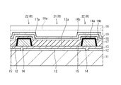
- FIG. FIG. 2 is a schematic cross-sectional view taken along line AA in FIG.
- FIG. 2 is a schematic cross-sectional view taken along the line BB in FIG.
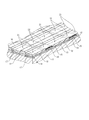
- It is a model perspective view which shows the structure of the organic electroluminescence display panel before a light emitting layer is formed.
- It is a model perspective view which shows the structure of the organic electroluminescent display panel after a light emitting layer was formed.
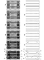
- It is a figure for demonstrating the discontinuation suppression effect of the light emitting layer by a film.
- It is a figure which shows the measurement result of a contact angle.
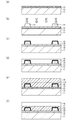
- (A) to (f) are AA cross-sectional schematic diagrams showing the manufacturing process of the organic EL display panel, (a) is a diagram showing the underlayer forming process, and (b) is the second partition forming process.
- (C) is a figure which shows a film formation process,
- (d) is a figure which shows a 1st partition formation process,
- (e) is a figure which shows an ink application process,
- (f) is a figure which shows an ink drying process.
- (A) to (f) are schematic cross-sectional views taken along the line BB showing the manufacturing process of the organic EL display panel, where (a) is a diagram showing the underlayer forming process and (b) is the second partition forming process.
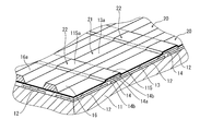
- FIG. 10 is a schematic perspective view for explaining a coating film according to Modification 1.
- FIG. 10 is a schematic cross-sectional view for explaining a coating film according to Modification 2.
- FIG. 5 is a block diagram illustrating a schematic configuration of an organic EL display device according to a second embodiment. It is a model perspective view for demonstrating the cause of the film thickness nonuniformity in the conventional organic EL display panel.
- An organic EL display panel includes a substrate, a base layer formed above the substrate, and a plurality of strips arranged in parallel so as to extend in the first direction above the base layer.
- a layer having a higher lyophilic property than the second partition wall is formed on at least the upper surface of the second partition wall.
- the coating film has higher lyophilicity than the underlayer or the same lyophilicity as the underlayer.
- the base layer includes tungsten oxide.
- the light emitting layer is formed by applying an ink containing an organic material in the gap and drying it, and the upper surface of the coating is in contact with the ink. The angle is 3 ° or less.
- the contact angle with respect to the ink on the upper surface of the underlying layer is about 3 °. Therefore, if the contact angle with respect to the ink on the upper surface of the coating is set to 3 ° or less, the lyophilic property is higher than that of the underlying layer. It can be made into a highly hydrophilic film or a lyophilic film of the same level as the underlayer. Accordingly, uneven brightness is more reliably suppressed.
- the coating is continuously formed on the second partition and the base layer along the first direction in the gap.
- the coating is formed only on the second partition in the gap.
- an organic EL display device includes the organic EL display panel. Since the organic EL display device according to the aspect includes the organic EL display panel in which unevenness in luminance is suppressed, high display quality is realized.
- upward does not indicate the upward direction (vertically upward) in absolute space recognition, but is defined by the relative positional relationship based on the stacking order in the stacking configuration. Further, the term “upward” is applied not only when there is a space between each other but also when they are in close contact with each other.
- Embodiment 1 an organic EL display panel according to Embodiment 1 which is one embodiment of the present invention will be described with reference to the drawings.
- drawing is a schematic diagram and the scale may differ from an actual thing.
- FIG. 1 is a schematic plan view showing a part of the organic EL display panel according to the first embodiment.
- an organic EL display panel 10 (hereinafter referred to as “panel 10”) is an organic EL display panel using an electroluminescence phenomenon of an organic compound.
- the panel 10 employs a line bank, and a plurality of first partition walls 16 are provided side by side, in which each strip extends in the column direction as the first direction (the vertical direction in FIG. 1). Further, when each of the adjacent first partition walls 16 is defined as a gap 20, the panel 10 has a configuration in which a large number of such first partition walls 16 and gaps 20 are alternately arranged.
- each of the gaps 20 a plurality of pixel regions 21 and a plurality of inter-pixel regions 22 between adjacent pixel regions 21 are alternately arranged in the column direction.
- a plurality of second partition walls 14 in which each strip extends in the row direction as the second direction (the left-right direction in the drawing of FIG. 1) are arranged in parallel.
- the first barrier ribs 16 provided in the column direction and the second barrier ribs 14 provided in the row direction are orthogonal to each other.
- the pixel area 21 includes a red pixel area 21R that emits red light, a green pixel area 21G that emits green light, and a blue pixel area 21B that emits blue light. Further, in the gap 20, there are a red gap 20R in which the internal pixel area 21 is a red pixel area 21R, a green gap 20G that is a green pixel area 21G, and a blue gap 20B that is a blue pixel area 21B. Further, the three pixel regions 21 of the red pixel region 21R, the green pixel region 21G, and the blue pixel region 21B are arranged in a row in the row direction to constitute one pixel.
- FIG. 2 is a schematic cross-sectional view taken along the line AA in FIG. 3 is a schematic cross-sectional view taken along the line BB in FIG.
- the panel 10 employs a so-called top emission type in which the upper side of the drawing in FIGS. 2 and 3 is the display surface.
- the upper side of FIG. 2 and FIG. 1 is the display surface.
- the panel 10 includes a substrate 11, a pixel electrode 12, a base layer 13, a second partition 14, a coating 15, a first partition 16, a light emitting layer 17, a counter electrode 18, and a sealing layer 19.
- the substrate 11 includes a base material (not shown), a thin film transistor (TFT) layer (not shown) formed on the base material, and an interlayer insulating layer (not shown) formed on the base material and the TFT layer. As shown).
- TFT thin film transistor
- the base material is a support member for the panel 10 and has a flat plate shape.
- a material having electrical insulation properties for example, a glass material, a resin material, a semiconductor material, a metal material coated with an insulating layer, or the like can be used.
- the TFT layer is composed of a plurality of TFTs and wirings formed on the upper surface of the substrate.
- the TFT electrically connects the pixel electrode 12 corresponding to itself and an external power source according to a drive signal from an external circuit of the panel 10 and has a multilayer structure such as an electrode, a semiconductor layer, and an insulating layer.
- the wiring electrically connects the TFT, the pixel electrode 12, an external power source, an external circuit, and the like.
- the interlayer insulating layer flattens at least the pixel region 21 on the upper surface of the substrate 11 where unevenness exists by the TFT layer.
- the interlayer insulating layer fills the space between the wiring and the TFT and electrically insulates the wiring and the TFT.
- a positive photosensitive organic material having electrical insulation specifically, an acrylic resin, a polyimide resin, a siloxane resin, a phenol resin, or the like can be used.
- the pixel electrode 12 is for supplying carriers to the light emitting layer 17. For example, when it functions as an anode, it supplies holes to the light emitting layer 17.
- the pixel electrode 12 has a flat plate shape. For example, when the connection with the TFT is made through a contact hole opened in the interlayer insulating layer, the pixel electrode 12 has an uneven portion along the contact hole.
- the pixel electrodes 12 are arranged on the substrate 11 at intervals in the column direction in each of the gaps 20.
- the material of the pixel electrode 12 since the panel 10 is a top emission type, it is preferable to use a conductive material having light reflectivity, for example, a metal such as silver, aluminum, molybdenum, or an alloy using these.
- the underlayer 13 is, for example, a hole injection layer in the present embodiment, and is formed as a continuous film above the pixel electrode 12, and electrically insulates between adjacent pixel electrodes 12. Yes. Thus, if the base layer 13 is formed as a continuous solid film, the manufacturing process can be simplified.
- the underlayer 13 is made of a transition metal oxide and functions as a hole injection layer.
- the transition metal is an element existing between the Group 3 element and the Group 11 element in the periodic table.
- transition metals tungsten, molybdenum, nickel, titanium, vanadium, chromium, manganese, iron, cobalt, niobium, hafnium, tantalum, and the like are preferable because they have high hole injectability after oxidation.
- tungsten is suitable for forming a hole injection layer having a high hole injection property.
- the underlayer 13 is not limited to the case of being made of a transition metal oxide, and may be made of an oxide other than the transition metal oxide, such as an alloy of a transition metal. Further, the underlayer 13 is not limited to the hole injection layer, and may be any layer as long as it is a layer formed between the pixel electrode 12 and the light emitting layer 17.
- the second partition wall 14 is for preventing ink containing an organic compound as a material from flowing in the column direction when the light emitting layer 17 is formed.
- the shape of the second partition wall 14 is a linear shape extending in the row direction, and the cross section in the column direction is a forward tapered trapezoidal shape that tapers upward.
- the second barrier ribs 14 are provided in a state along the row direction perpendicular to the column direction so as to penetrate the first barrier ribs 16, and each upper surface is located at a position lower than the upper surface 16 a of the first barrier rib 16. 14a.
- an electrically insulating material such as an inorganic material such as silicon oxide or silicon nitride, or an organic material such as an acrylic resin, a polyimide resin, a siloxane resin, or a phenol resin is used. be able to.
- the coating 15 is for preventing the light emitting layer 17 from being interrupted above the second partition 14, and is formed on the second partition 14. Specifically, in the gap 20, as shown in FIG. 3, the underlying layer is formed on the upper surface 14 a and the side surface 14 b of the second partition wall 14 existing in the inter-pixel region 22, and exists in the pixel region 21. 13 is not formed on the upper surface 13a.
- a material of a coating type organic functional layer can be used as the material of the coating 15.
- a coating type hole injection material such as PEDOT: PSS can be used.
- the coating 15 is formed by, for example, applying an ink obtained by dissolving a material of a coating-type organic functional layer in a solvent to the upper surface 14a and the side surface 14b of the second partition wall 14 and drying it.
- the ink for the coating film 15 preferably has good wettability with respect to the surface (the upper surface 14a and the side surface 14b) of the second partition wall 14.
- the material of the coating 15 has good wettability with respect to the layer ink (for example, the light emitting layer 17 ink or the interlayer ink (CHB)) formed on the coating 15. Is preferred.
- the polar solvent is used for the ink for the films 15. This is because when the material of the second partition wall 14 is an organic material, a hydroxyl group is present on the surface of the second partition wall 14, and therefore wettability is improved when a polar solvent is used.
- the coating film 15 is formed of a material having higher lyophilicity than the material of the second partition wall 14, and is more lyophilic than the second partition wall 14. Therefore, the light emitting layer 17 is difficult to be interrupted above the second partition 14. This will be described later.
- the first partition 16 is for restricting the flow of ink in the row direction in the gap 20 when the light emitting layer 17 is formed.
- the shape of the first partition wall 16 is a linear shape extending in the column direction, and the cross section in the row direction is a forward tapered trapezoidal shape that tapers upward.
- the first partition 16 is formed on the base layer 13 so as to sandwich each pixel electrode 12 from the row direction and over the second partition 14.
- the material of the first partition 16 for example, an organic material such as an acrylic resin, a polyimide resin, a siloxane resin, or a phenol resin can be used.
- the 1st partition 16 has the tolerance to an organic solvent, and is formed with the material which does not deform
- the light emitting layer 17 is a layer made of an organic compound and has a function of emitting light by recombining holes and electrons inside. Each light emitting layer 17 is linearly provided in the gap 20 so as to extend in the column direction, and is located on the base layer 13 in the pixel region 21 and on the film 15 in the inter-pixel region 22. .
- the light emitting layer 17 emits light only from the portion to which carriers are supplied from the pixel electrode 12. Therefore, as shown in FIG. 3, only the portion of the pixel region 21 on the pixel electrode 12 in the light emitting layer 17 emits light, and the portion of the inter-pixel region 22 on the second partition 14 does not emit light.
- the light emitting layer 17 extends not only to the pixel region 21 but also to the adjacent inter-pixel region 22.
- the ink applied to the pixel region 21 can flow in the column direction through the ink applied to the inter-pixel region 22, and the film thickness between the pixel regions 21 in the column direction is increased. Can be leveled.
- the flow of ink is moderately suppressed by the second partition wall 14. Therefore, large film thickness unevenness hardly occurs in the column direction.
- a light emitting organic material that can be formed using a wet process is used.
- known fluorescent materials and phosphorescent materials such as compounds, derivatives and complexes described in Japanese Patent Publication (JP-A-5-163488) can be used.
- the counter electrode 18 is paired with the pixel electrode 12 to form an energization path by sandwiching the light emitting layer 17 and supply carriers to the light emitting layer 17. For example, when the counter electrode 18 functions as a cathode, electrons are supplied to the light emitting layer 17. Supply.
- the counter electrode 18 is formed along the upper surface 17 a of each light emitting layer 17 and the surface of each first partition 16 exposed from the light emitting layer 17, and serves as a common electrode for each light emitting layer 17.
- the material of the counter electrode 18 since the panel 10 is a top emission type, a conductive material having optical transparency is used.
- a conductive material having optical transparency is used.
- ITO indium tin oxide
- IZO indium zinc oxide
- the sealing layer 19 is for suppressing the light emitting layer 17 from being deteriorated by contact with moisture or air.
- the sealing layer 19 is provided over the entire panel 10 so as to cover the upper surface of the counter electrode 18.
- a light transmissive material such as silicon nitride or silicon oxynitride is used.
- a color filter or an upper substrate may be installed and bonded on the sealing layer 19. Thereby, adjustment of the display color of the panel 10, improvement of rigidity, prevention of intrusion of moisture, air, and the like can be achieved.
- FIG. 4 is a schematic perspective view showing the structure of the organic EL display panel before the light emitting layer is formed.
- FIG. 5 is a schematic perspective view showing the structure of the organic EL display panel after the light emitting layer is formed.
- the coating 15 having higher lyophilicity than the second partition 14 is formed on the second partition 14.
- the high lyophilic property means that the affinity of the light emitting layer 17 with the ink is high, that is, the wettability with respect to the ink is good.
- the lyophilicity of the coating 15 is higher than the lyophilicity of the second partition 14, the lyophilicity of the upper surface 15 a of the coating 15 is higher than the lyophilicity of the upper surface 14 a of the second partition 14. Therefore, the upper surface 15 a of the coating 15 has better wettability with respect to ink than the upper surface 14 a of the second partition wall 14.
- a coating having a higher lyophilic property than second partition 14 is formed on upper surface 14 a of second partition 14 before light emitting layer 17 is formed.
- 15 is formed, the wettability of the inter-pixel region 22 is improved by the coating 15. For this reason, it is easy for the ink in the middle of drying applied to the gap 20 between the first partition walls 16 to stay in the inter-pixel region 22, and it is possible to maintain the state where the ink in the adjacent pixel region 21 is connected in a wet state. it can. Therefore, the light emitting layer 17 is not easily interrupted in the inter-pixel region 22 above the second partition 14. As a result, a uniform liquid amount can be applied to each pixel region 21, and the light emitting layer 17 having a uniform film thickness can be obtained.
- the entire upper surface 17 a is flat. Therefore, the film thickness of the light emitting layer 17 in the pixel region 21. Is even. That is, the ink is applied to each pixel region 21 as much as planned, and the application amount is sufficiently leveled between the pixel regions 21. Since the coating amount is the same, the film thickness of the light emitting layer 17 in each pixel region 21 is uniform.
- the above configuration suppresses uneven brightness when the panel is lit.
- the above-described configuration may change the film thickness of each color light-emitting layer for optical adjustment or the like in each pixel of RGB, and is particularly effective in such a case. This is because a situation in which the film thickness must be considerably reduced depending on the color due to optical adjustment is likely to occur, and the light emitting layer 17 is likely to be interrupted in that color because the amount of ink applied is reduced.
- the lyophilicity of the second partition wall 14 is preferably larger than the lyophilicity of the first partition wall 16. If so, it is possible to suppress the occurrence of ink breaks and uneven film thickness of the pixel region 21.
- the surface of the first partition 16 is often made less lyophilic so that the ink does not flow over the first partition 16 (the liquid repellency is often improved).
- the lyophilicity of the surface of the second partition wall 14 is less than or equal to the lyophilicity of the surface of the first partition wall 16, the ink reaches the portion where the surface of the second partition wall 14 and the surface of the first partition wall 16 are joined. Becomes difficult to spread, causing ink interruption and unevenness in the film thickness of the pixel region 21.
- FIG. 6 is a diagram for explaining the effect of suppressing discontinuity of the light emitting layer by the coating.
- a photographic image obtained by photographing the substrate 11 after the formation of the light emitting layer 17 from above is displayed on the upper stage.
- the light emitting layer 17 is formed by applying 2 drops, 3 drops, 4 drops, 5 drops, 6 drops or 7 drops of ink to the pixel region 21 in order from the left.
- the light emitting layers 17 of the three pixel regions 21 adjacent in the row direction are shown, and the left two of them are on both sides (upper and lower sides) of the pixel region 21.
- the film 15 is formed in the inter-pixel region 22 positioned, and the remaining one on the right is the film 15 not formed in the inter-pixel region 22. That is, the effect of the coating 15 can be understood by comparing the state of the light emitting layer 17 in the inter-pixel region 22 between the left two and the right one.
- the lower part shows the trace of the outline of the light emitting layer 17 that can be seen from the upper photographic image.
- the light-emitting layer 17 is interrupted due to the poor wettability of the inter-pixel region 22, or the light emitting layer 17 is not interrupted.
- the width is narrowed.
- a defect 17b is generated in the light emitting layer 17 in the inter-pixel region 22 where the coating film 15 is not formed. Further, when 2 to 3 drops of ink are applied, the light emitting layer 17 is interrupted in the inter-pixel region 22 where the coating film 15 is not formed.
- the light emitting layer 17 is not interrupted even if the coating amount is two drops.
- the coating 15 is formed on the second partition wall 14, the light emitting layer 17 can be prevented from being interrupted in the inter-pixel region 22 even if the amount of ink applied is small.
- the wettability with respect to ink can be evaluated by measuring the contact angle with respect to ink.
- FIG. 7 is a diagram for explaining a method of measuring a contact angle with respect to ink.
- a layer for which wettability is to be evaluated is formed on a substrate or the like, and 0.5 to 1.0 ⁇ l of ink is dropped on the upper surface of the layer to form a droplet.
- the camera with the camera from the horizontal direction.
- the radius r of the bottom surface of the droplet and the height h vertical distance from the top surface of the layer to the top of the droplet
- the radius r and The angle ⁇ 1 is obtained by substituting the height h into Equation 1 below.
- a value twice the angle ⁇ 1 was defined as the contact angle ⁇ .
- ⁇ 1 tan ⁇ 1 (h / r) Equation 1
- ⁇ ⁇ 1 ⁇ 2 Equation 2
- wettability is so high that a contact angle is small.
- lyophilicity is so high that a contact angle is small.
- sample 1 a semi-finished product of the panel 1 according to Embodiment 1 before the first partition 16 and the light emitting layer 17 were formed was produced.
- the second partition 14 is subjected to UV irradiation and baking to reduce the contact angle. Further, a film 15 is formed on the second partition wall 14 in order to further reduce the contact angle.
- Sample 2 was a semi-finished product before the first partition 16 and the light-emitting layer were formed as in Sample 1, but a sample in which the coating 15 was not formed on the second partition 14 was produced.
- the second partition wall 14 is subjected to UV irradiation and baking treatment, but unlike sample 1, no coating 15 is formed.
- Sample 3 was a semi-finished product before the coating 15 was formed, and the second partition 14 was not subjected to UV irradiation and baking treatment. Unlike the sample 1, the sample 3 is not subjected to the UV irradiation and baking treatment on the second partition wall 14 and further has no coating 15 formed thereon.
- the wettability was evaluated by measuring the contact angle with respect to the ink by the method described above and determining that the smaller the contact angle, the better the wettability.
- FIG. 8 is a diagram showing the measurement results of the contact angle. As shown in FIG. 8, the contact angle of sample 3 was 5.9 °, whereas the contact angle of sample 2 was 3.1 °. Sample 2 was more wettable than sample 3 it was high. Since the difference between sample 3 and sample 2 is whether or not the second partition 14 is subjected to UV irradiation and baking, it was confirmed that wettability was improved by performing UV irradiation and baking.
- the contact angle of sample 1 was 1.5 °, which was smaller than the contact angle of sample 2. From this, it was confirmed that the wettability was further improved by forming the coating film 15.
- FIGS. 9A to 9F are schematic cross-sectional views taken along the line AA showing the manufacturing process of the organic EL display panel.
- 10A to 10F are schematic cross-sectional views taken along the line BB showing the manufacturing process of the organic EL display panel.
- the substrate 11 is prepared. Specifically, for example, a necessary film is formed on a substrate by sputtering, CVD (Chemical Vapor Deposition), spin coating, or the like, and the film is patterned by photolithography to form a TFT layer and an interlayer insulating layer. Form. At this time, plasma treatment, ion implantation, baking, or the like may be performed as necessary.
- the pixel electrode 12 is formed on the substrate 11, and the pixel electrode 12 is formed. Specifically, for example, a metal film is first formed on the substrate 11 by vacuum deposition or sputtering. Next, the metal film is patterned by a photolithography method, a plurality of pixel electrodes 12 are arranged in the column direction at intervals on the substrate 11, and a plurality of columns of such pixel electrodes 12 are arranged in parallel. In this way, the pixel electrodes 12 that are two-dimensionally arranged on the substrate 11 are formed.
- a base layer 13 is formed on the substrate 11 after the pixel electrode 12 is formed. Specifically, for example, a solid oxide layer is formed on the substrate 11 so as to cover all the pixel electrodes 12 by sputtering.
- the second partition 14 is formed on the base layer 13. Specifically, for example, an inorganic insulating film (silicon oxide or the like) is formed on the base layer 13 by a CVD method. Then, the inorganic insulating film is patterned by photolithography, and a linear second partition 14 is formed so as to extend in the row direction at a position sandwiching each of the 12 rows of pixel electrodes.
- an inorganic insulating film silicon oxide or the like
- UV irradiation and baking are not essential and optional.
- the UV irradiation conditions are, for example, about 60 seconds to 180 seconds using a UV ozone cleaner (UV-1, manufactured by SAMCO).
- the baking conditions are, for example, 200 ° C. to 250 ° C. and about 10 minutes to 30 minutes.
- an ink containing a coating type organic functional layer material is applied onto the second partition 14 and dried to form a coating 15.
- ink is applied on the base layer 13 and the second partition 14 by a spin coating method.
- patterning is performed by a photolithography method, and the film 15 is formed only on the upper surface 14a and the side surface 14b of the second partition 14.
- the first partition 16 is formed on a part on the base layer 13 and a part on the second partition 14.
- a positive photosensitive organic material such as an acrylic resin
- the thickness of the applied material is made larger than the thickness of the second partition 14.
- the photosensitive organic material is patterned by a photolithography method, and the linear first barrier ribs 16 are formed so as to extend in the column direction at positions sandwiching the pixel electrode 12 columns.
- the first partition 16 may be subjected to a surface treatment with an alkaline solution, water, an organic solvent, plasma, or the like to impart liquid repellency to the ink applied in the subsequent steps on the surface of the first partition 16. . By doing in this way, it can suppress that an ink flows over the 1st partition 16 in the subsequent light emitting layer formation process.
- the gap 20 between the adjacent first partition walls 16 is formed, and the columns formed by the pixel region 21 and the inter-pixel region 22 are respectively present in the gap 20.
- the ink 17A is applied in the gap 20.
- an ink 17A is prepared by mixing an organic compound serving as a material of the light emitting layer 17 and a solvent at a predetermined ratio, and this ink 17A is applied in the gap 20 using an ink jet method.
- the ink 17A can flow over the second partition wall 14.
- the light emitting layer 17 is formed by evaporating and drying the solvent contained in the ink 17A.
- a dispenser method, a nozzle code method, a spin coating method, a printing method, or the like may be used as a method for applying the ink 17A.
- the light emitting layer 17 since the light emitting layer 17 has the pixel regions 21 of three colors of red, green, and blue, they are formed using different inks 17A. Specifically, for example, using a nozzle (ejection port) that ejects only the ink 17A corresponding to any of red, green, and blue, a method of sequentially applying the three colors of ink 17A, or red, green, and blue There is a method of simultaneously applying the three color inks 17A using a triple nozzle capable of simultaneously discharging the inks 17A corresponding to the respective colors.
- the panel 10 employs a line bank
- a plurality of nozzles that eject only the same color ink 17A are arranged in the column direction, and the ink 17A is ejected into the gap 20 while moving in the direction intersecting the column direction.
- a method of forming the light emitting layer 17 is preferable. According to this method, since a plurality of nozzles are used first, the application time of the ink 17A is shortened, and the process can be shortened.
- the ink 17A ejected from a plurality of nozzles is connected in the column direction by the gap 20, even if the ejection amount of the ink 17A from each nozzle varies, the ink 17A can flow in the column direction thereafter, and the coating amount is increased. By leveling, it is possible to reduce the occurrence of film thickness unevenness between the pixel regions 21, that is, luminance unevenness.
- the light emitting layer 17 is formed in the gap 20 as shown in FIGS. 9 (f) and 10 (f).
- the linear light emitting layer 17 is formed across the pixel region 21 where the base layer 13 not covered with the second partition 14 exists and the inter-pixel region 22 where the second partition 14 and the coating 15 exist. can do.
- the counter electrode 18 is formed along the upper surface 17 a of each light emitting layer 17 and the surface of each first partition 16 exposed from the light emitting layer 17.
- a light-transmitting conductive material such as ITO or IZO along the upper surface 17a of each light-emitting layer 17 and the surface of each first partition wall 16 exposed from the light-emitting layer 17 by, for example, vacuum deposition or sputtering.
- a film made of a material is formed.
- a sealing layer 19 that covers the upper surface of the counter electrode 18 is formed.
- an inorganic insulating film such as silicon oxide is formed on the counter electrode 18 by, for example, a sputtering method or a CVD method.
- Embodiment 1 the panel 10 according to one embodiment of the present invention has been described.
- the present invention is not limited to the above embodiment except for essential characteristic components.
- it is realized by arbitrarily combining the components and functions in each embodiment without departing from the scope of the present invention, or the form obtained by subjecting each embodiment to various modifications conceived by those skilled in the art. Forms are also included in the present invention.
- the modification of the panel 10 is demonstrated as an example of such a form.
- Modification 1 The panel according to Modification 1 is different from the panel 10 according to Embodiment 1 in that a film is also formed between the base layer and the light emitting layer in the pixel region.
- Other configurations are basically the same as those of the panel 10 according to the first embodiment. Therefore, only the above differences will be described, and descriptions of other configurations will be omitted.
- FIG. 11 is a schematic perspective view for explaining the coating film according to the first modification.
- the coating 115 is formed in the gap 20 between the adjacent first partition walls 16 across the plurality of pixel regions 21 arranged in the column direction. More specifically, it is formed not only in each pixel region 21 in the same gap 20 but also in each inter-pixel region 22 existing between adjacent pixel regions 21. Further, it is formed below the first partition 16. That is, the coating 115 is formed as a solid film over the entire substrate 11 and is not only formed over the second partition 14, but also the upper surface 13 a of the base layer 13 between the adjacent second partitions 14. Also formed.
- the film may be formed in a band shape only in the gap 20 between the first partition walls 16. That is, a configuration in which no film is formed below the first partition 16 may be employed.
- the coating 115 is more lyophilic than the second partition 14. Therefore, the upper surface 115 a of the coating 115 is more lyophilic than the upper surface 13 a of the base layer 13.
- a material constituting the coating 115 the same material as the material of the coating 15 according to Embodiment 1 can be used.
- the wettability of the pixel region 21 and the wettability of the inter-pixel region 22 are the same, so that the luminance unevenness is further suppressed. Further, since fine patterning when forming the coating 115 is not necessary, the manufacturing process can be simplified.
- Modification 2 The panel according to the modification 2 is different from the panel 10 according to the first embodiment in that the film is formed only on the upper surface of the second partition.
- Other configurations are basically the same as those of the panel 10 according to the first embodiment. Therefore, only the above differences will be described, and descriptions of other configurations will be omitted.
- FIG. 12 is a schematic cross-sectional view for explaining a coating film according to Modification 2.
- the coating 215 is formed on the upper surface 14 a of the second partition 14, but is not formed on the side surface 14 b of the second partition 14.
- the coating 215 is not necessarily formed on the entire surface of the second partition 14 (the entire surface of the second partition 14 on the light emitting layer 17 side), and is formed on at least the upper surface 14a of the second partition 14. It only has to be. This is because if the coating 215 is formed on the upper surface 14a of the second partition wall 14, the ink breaks above the second partition wall 14 can be effectively suppressed.
- the coating 215 is preferably formed on the entire upper surface 14a of the second partition wall 14, but is not necessarily formed on the entire upper surface 14a, and may be formed on a part of the upper surface 14a. Good.
- the coating 215 is more lyophilic than the second partition 14. Therefore, the upper surface 215 a of the coating 215 is more lyophilic than the upper surface 13 a of the base layer 13.
- a material constituting the film 215 the same material as the material of the film 15 according to Embodiment 1 can be used.
- the present invention is not limited to this.
- a configuration including a hole injection layer, a hole transport layer, an electron transport layer, an electron injection layer, or the like, or a configuration including a plurality or all of them at the same time may be used.
- these layers do not need to consist of organic compounds, and may be composed of inorganic substances.
- the light emitting layer may be one type, or the light emitting layer may be four types that emit red, green, blue, and yellow.
- all the pixel regions 21 in the gap 20 emit light of the same color, but the present invention is not limited to this.
- a configuration including a gap 20 in which red pixel areas 21R and blue pixel areas 21B are alternately arranged and a green gap 20G may be employed.
- the pixel regions 21 are arranged in a matrix, but the present invention is not limited to this.
- the present invention is effective even for a configuration in which the pixel regions are shifted by a half pitch in the column direction between adjacent gaps.
- a slight shift in the column direction is difficult to distinguish visually, and even if the film thickness unevenness is arranged on a straight line (or zigzag) having a certain width, it is visually stripped. Therefore, even in such a case, the display quality of the display panel can be improved by suppressing the luminance unevenness from being arranged in a staggered manner.
- the pixel electrodes 12 in which the base layer 13 is arranged in the row direction are electrically insulated, but the present invention is not limited to this.
- the pixel electrodes 12 are arranged in all the gaps 20, but the present invention is not limited to this configuration.
- the second partition 14 has a shape that can be distinguished from other components such as the base layer 13 and the first partition 16, but the present invention is not limited to this.
- a part of the foundation layer may correspond to the second partition wall.
- the structure and properties such as the height from the upper surface of the substrate, the length in the direction intersecting the first partition, and the liquid repellency are different from others, so that the ink in the column direction If there is an inter-pixel region that has a greater effect of regulating the flow than the other, the second partition wall is present in the inter-pixel region.
- even if there is a portion having a slight flow restriction effect as in the base layer 13 according to the first embodiment it does not immediately become an inter-pixel region where the second partition wall exists.
- the panel 10 has a top emission type configuration, but a bottom emission type may be employed. In that case, it is possible to appropriately change each configuration.
- the panel 10 has an active matrix type configuration.
- the present invention is not limited to this, and may be a passive matrix type configuration, for example.
- a plurality of linear electrodes parallel to the extending direction of the first partition walls and a plurality of linear electrodes orthogonal to the extending direction of the first partition walls may be provided side by side so as to sandwich the light emitting layer.
- the linear electrode orthogonal to the extending direction of the first partition is on the lower side, a plurality of lower electrodes are arranged in the extending direction of the first partition at intervals in each gap. It becomes one aspect
- the substrate 11 has the TFT layer.
- the substrate 11 is not limited to the TFT layer.
- Embodiment 2 an organic EL display device according to Embodiment 2 which is one embodiment of the present invention will be described with reference to FIGS.
- FIG. 13 is a block diagram showing a schematic configuration of the organic EL display device according to the second embodiment.
- the organic EL display device 1 according to the second embodiment is an organic EL display device including the panel 10 according to the first embodiment.
- the organic EL display device 1 includes a drive control unit 30 connected to the panel 10.
- the drive control unit 30 includes four drive circuits 31 to 34 and a control circuit 35.
- the arrangement of the drive control unit 30 with respect to the panel 10 is not limited to this.
- a voltage is applied to the predetermined pixel electrode 12 via the TFTs in the substrate 11 of the panel 10 by the drive circuits 31 to 34 by the active matrix method.
- a current flows between the predetermined pixel electrode 12 and the counter electrode 18, and the light emitting layer 17 in the pixel region 21 corresponding to the predetermined pixel electrode 12 emits light.
- the panel 10 as a whole can display a colored image.
- the organic EL display device 1 includes a panel 10 in which uneven brightness is suppressed. Therefore, the organic EL display device 1 can achieve high display quality.
- the organic EL display panel and the organic EL display device according to the present invention can be widely used in various electronic devices having devices such as a television set, a personal computer, a mobile phone, and other display panels.
Landscapes
- Engineering & Computer Science (AREA)
- Microelectronics & Electronic Packaging (AREA)
- Manufacturing & Machinery (AREA)
- Electroluminescent Light Sources (AREA)
Abstract
Description
本発明の一態様に係る有機EL表示パネルは、基板と、基板の上方に形成された下地層と、前記下地層の上方に各々が第1方向に延伸するよう並設された複数条の第1隔壁と、前記下地層の上方に各々が前記第1方向と交差する第2方向に延伸するように並設され、且つ、各々が前記第1隔壁の上面よりも低い位置に上面を有する複数条の第2隔壁と、前記下地層の上方であって隣り合う前記第1隔壁間の間隙内に、前記複数条の第2隔壁を乗り越えるようにして前記第1方向に沿って形成された発光層とを備え、前記第2隔壁の少なくとも上面には、前記第2隔壁よりも親液性の高い被膜が形成されている。この構成であれば、第1隔壁間の間隙に塗布された乾燥途中のインクが、第2隔壁の上方にとどまり易いため、発光層が第2隔壁の上方で途切れ難い。したがって、輝度むらが抑制される。
以下では、本発明の一態様である実施の形態1に係る有機EL表示パネルについて、図面を用いて説明する。なお、図面は模式図であって、その縮尺は実際とは異なる場合がある。
図1は、実施の形態1に係る有機EL表示パネルの一部を示す模式平面図である。図1に示すように、有機EL表示パネル10(以下、「パネル10」という。)は、有機化合物の電界発光現象を利用した有機EL表示パネルである。パネル10では、ラインバンクを採用し、各条が第1方向としての列方向(図1の紙面上下方向)に延伸する第1隔壁16が複数並設されている。また、隣り合う第1隔壁16間の各々を、間隙20と定義した場合、パネル10は、このような第1隔壁16と間隙20が交互に多数並んだ構成を有する。
パネル10の各部構成を図2及び図3を用いて説明する。図2は、図1におけるA-A断面模式図である。図3は、図1におけるB-B断面模式図である。
基板11は、基材(不図示)と、基材上に形成された薄膜トランジスタ(TFT:Thin Film Transistor) 層(不図示)と、基材上及びTFT層上に形成された層間絶縁層(不図示)とを有する。
画素電極12は、発光層17へキャリアを供給するためのものであり、例えば陽極として機能した場合は、発光層17へ正孔を供給する。画素電極12の形状は、平板状であるが、例えば、TFTとの接続を層間絶縁層に開口したコンタクトホールを通じて行う場合は、コンタクトホールに沿った凹凸部を有する。画素電極12は、間隙20のそれぞれにおいて、列方向に間隔をあけて基板11上に配されている。
下地層13は、例えば、本実施の形態では正孔注入層であって、画素電極12の上方に連続したべた膜として形成されており、隣接する画素電極12の間を電気的に絶縁している。このように、下地層13が連続したべた膜として形成されていれば、製造工程の簡略化を図ることができる。
第2隔壁14は、発光層17形成時に、その材料となる有機化合物を含んだインクが列方向へ流動することを抑制するためのものである。第2隔壁14の形状は、行方向に延伸する線状であり、列方向の断面は上方を先細りとする順テーパー台形状である。第2隔壁14は、各第1隔壁16を貫通するようにして、列方向と直交する行方向に沿った状態で設けられており、各々が第1隔壁16の上面16aよりも低い位置に上面14aを有する。
被膜15は、発光層17が第2隔壁14の上方で途切れるのを防止するためのものであって、第2隔壁14上に形成されている。具体的には、間隙20内において、図3に示すように、画素間領域22に存在する第2隔壁14の上面14aと側面14bの上に形成されており、画素領域21に存在する下地層13の上面13aの上には形成されていない。
第1隔壁16は、発光層17形成時に、インクが間隙20内において行方向へ流動することを規制するためのものである。第1隔壁16の形状は、列方向に延伸する線状であり、行方向の断面は上方を先細りとする順テーパーの台形状である。第1隔壁16は、各画素電極12を行方向から挟むように、且つ、各第2隔壁14を乗り越えるように、下地層13上に形成されている。
発光層17は、有機化合物からなる層であり、内部で正孔と電子が再結合することで光を発する機能を有する。各発光層17は、間隙20内に列方向に延伸するように線状に設けられており、画素領域21においては下地層13上に位置し、画素間領域22においては被膜15上に位置する。
対向電極18は、画素電極12と対になって発光層17を挟むことで通電経路を作り、発光層17へキャリアを供給するものであり、例えば陰極として機能した場合は、発光層17へ電子を供給する。対向電極18は、各発光層17の上面17a及び発光層17から露出する各第1隔壁16の表面に沿って形成され、各発光層17に共通の電極となっている。
封止層19は、発光層17が水分や空気などに触れて劣化することを抑制するためのものである。封止層19は、対向電極18の上面を覆うようにパネル10全面に渡って設けられている。封止層19の材料としては、パネル10がトップエミッション型であるため、例えば窒化シリコン、酸窒化シリコンなどの光透過性材料が用いられる。
なお、図2及び図3では図示しないが、封止層19の上にカラーフィルタや上部基板を設置・接合してもよい。これにより、パネル10の表示色の調整や、剛性向上、水分や空気などの侵入防止などを図ることができる。
パネル10の要部構成を図4及び図5を用いて説明する。図4は、発光層が形成される前の有機EL表示パネルの構造を示す模式斜視図である。図5は、発光層が形成された後の有機EL表示パネルの構造を示す模式斜視図である。
被膜15による発光層17の途切れ抑制効果を実験により評価した。
インクに対する濡れ性は、インクに対する接触角を測定することにより評価できる。
θ=θ1×2 ・・・・・・・・ 式2
なお、接触角が小さいほど濡れ性が高いと評価できる。また、接触角が小さいほど親液性が高いと評価できる。
被膜15による効果、及び、後述するUV照射及びベーク処理を施す効果を確認するために、サンプル1~3を作成し、それぞれのサンプルの画素間領域22の濡れ性を評価した。
パネル10の製造方法について図9及び図10を用いて説明する。図9(a)~(f)は、有機EL表示パネルの製造工程を示すA-A断面模式図である。図10(a)~(f)は、有機EL表示パネルの製造工程を示すB-B断面模式図である。
まず基板11を用意する。具体的には、例えば、基材にスパッタリング法、CVD(Chemical Vapor Deposition)法、スピンコート法などによって必要な膜を形成し、フォトリソグラフィー法によって膜をパターニングすることでTFT層及び層間絶縁層を形成する。この際、必要に応じて、プラズマ処理、イオン注入、ベーキングなどの処理を行ってもよい。
次に、基板11上に画素電極12を形成し、画素電極12を形成する。具体的には、例えば、まず真空蒸着法又はスパッタリング法によって基板11上に金属膜を形成する。次に、フォトリソグラフィー法によって金属膜をパターニングし、基板11上に間隔をあけて列方向に画素電極12を複数並べ、さらにそのような画素電極12の列を複数並設する。このようにして、基板11上に二次元配置された画素電極12を形成する。
次に、図9(a)及び図10(a)に示すように、画素電極12を形成後の基板11上に下地層13を形成する。具体的には、例えば、スパッタリング法により全ての画素電極12を覆い隠すようにべた膜の酸化物層を基板11上に成膜する。
次に、図9(b)及び図10(b)に示すように、下地層13上に第2隔壁14を形成する。具体的には、例えば、CVD法によって下地層13上に、無機絶縁膜(酸化シリコンなど)を形成する。そして、フォトリソグラフィー法によって無機絶縁膜をパターニングし、画素電極12行のそれぞれを挟む位置に、行方向に延伸するように線状の第2隔壁14を形成する。
次に、図9(d)及び図10(d)に示すように、下地層13上の一部及び第2隔壁14上の一部に第1隔壁16を形成する。具体的には、例えば、スピンコート法によって、ポジ型の感光性有機材料(アクリル系樹脂など)を塗布する。この際、塗布した材料の膜厚は第2隔壁14の膜厚よりも大きくする。そして、フォトリソグラフィー法によって感光性有機材料をパターニングし、画素電極12列のそれぞれを挟む位置に、列方向に延伸するように線状の第1隔壁16を形成する。
次に、図9(e)及び図10(e)に示すように、間隙20内にインク17Aを塗布する。具体的には、例えば、発光層17の材料となる有機化合物と溶媒とを所定の比率で混合してインク17Aを作成し、インクジェット法を用いて、このインク17Aを間隙20内に塗布する。インク17Aの上面が、第2隔壁14の上面14aよりも高くなるよう塗布することで、第2隔壁14を乗り越えるインク17Aの流動を可能にしている。そして、インク17Aに含まれる溶媒を蒸発乾燥させることにより、発光層17を形成する。なお、インク17Aの塗布方法としては、ディスペンサー法、ノズルコード法、スピンコート法、印刷法などを用いてもよい。
その後、各発光層17の上面17a及び発光層17から露出する各第1隔壁16の表面に沿って、対向電極18を形成する。具体的には、例えば、真空蒸着法又はスパッタリング法などによって、各発光層17の上面17a及び発光層17から露出する各第1隔壁16の表面に沿って、ITO、IZOなどの光透過性導電材料からなる膜を形成する。
次に、対向電極18の上面を覆う封止層19を形成する。具体的には、例えば、スパッタリング法又はCVD法によって、対向電極18上に無機絶縁膜(酸化シリコンなど)を形成する。
実施の形態1では、本発明の一態様に係るパネル10を説明したが、本発明は、その本質的な特徴的構成要素を除き、以上の実施の形態に何ら限定を受けるものではない。例えば、各実施の形態に対して当業者が思いつく各種変形を施して得られる形態や、本発明の趣旨を逸脱しない範囲で各実施の形態における構成要素及び機能を任意に組み合わせることで実現される形態も本発明に含まれる。以下では、そのような形態の一例として、パネル10の変形例を説明する。
変形例1に係るパネルは、画素領域における下地層と発光層との間にも被膜が形成されている点において実施の形態1に係るパネル10とは相違する。その他の構成については基本的に実施の形態1に係るパネル10と同様である。したがって、上記相違点についてのみ説明し、その他の構成についての説明は省略する。
変形例2に係るパネルは、被膜が第2隔壁の上面のみに形成されている点において実施の形態1に係るパネル10とは相違する。その他の構成については基本的に実施の形態1に係るパネル10と同様である。したがって、上記相違点についてのみ説明し、その他の構成についての説明は省略する。
上記実施の形態1では、画素電極12と対向電極18の間に、下地層13及び発光層17のみが存在する構成であったが、本発明はこれに限られない。例えば、正孔注入層、正孔輸送層、電子輸送層、電子注入層などを備える構成や、これらの複数又は全部を同時に備える構成であってもよい。また、これらの層はすべて有機化合物からなる必要はなく、無機物などで構成されていてもよい。
以下では、本発明の一態様である実施の形態2に係る有機EL表示装置について、図13を用いて説明する。
10 有機EL表示パネル
11 基板
13 下地層
14 第2隔壁
14a 上面
15 被膜
16 第1隔壁
16a 上面
17 発光層
Claims (7)
- 基板と、
基板の上方に形成された下地層と、
前記下地層の上方に各々が第1方向に延伸するよう並設された複数条の第1隔壁と、
前記下地層の上方に各々が前記第1方向と交差する第2方向に延伸するように並設され、且つ、各々が前記第1隔壁の上面よりも低い位置に上面を有する複数条の第2隔壁と、
前記下地層の上方であって隣り合う前記第1隔壁間の間隙内に、前記複数条の第2隔壁を乗り越えるようにして前記第1方向に沿って形成された発光層と
を備え、
前記第2隔壁の少なくとも上面には、前記第2隔壁よりも親液性の高い被膜が形成されている
有機EL表示パネル。 - 前記被膜は、前記下地層よりも親液性が高い、又は、前記下地層と同程度の親液性である
請求項1に記載の有機EL表示パネル。 - 前記下地層は酸化タングステンを含む
請求項1または2に記載の有機EL表示パネル。 - 前記発光層は、前記間隙内に有機材料を含むインクを塗布し、これを乾燥してなり、
前記被膜の上面は、前記インクに対する接触角が3°以下である
請求項3に記載の有機EL表示パネル。 - 前記被膜は、前記間隙内において前記第1方向に沿って前記第2隔壁上及び前記下地層上に連続して形成されている
請求項1から請求項4のいずれかに記載の有機EL表示パネル。 - 前記被膜は、前記間隙内において前記第2隔壁上にのみ形成されている
請求項1から請求項4のいずれかに記載の有機EL表示パネル。 - 請求項1から請求項6のいずれかに記載の有機EL表示パネルを備える、
有機EL表示装置。
Priority Applications (3)
| Application Number | Priority Date | Filing Date | Title |
|---|---|---|---|
| US15/123,390 US9799711B2 (en) | 2014-03-04 | 2015-02-23 | Organic EL display panel and organic EL display device |
| JP2016506116A JP6337088B2 (ja) | 2014-03-04 | 2015-02-23 | 有機el表示パネル及び有機el表示装置 |
| US15/709,717 US10269878B2 (en) | 2014-03-04 | 2017-09-20 | Organic EL display panel and organic EL display device |
Applications Claiming Priority (2)
| Application Number | Priority Date | Filing Date | Title |
|---|---|---|---|
| JP2014041595 | 2014-03-04 | ||
| JP2014-041595 | 2014-03-04 |
Related Child Applications (2)
| Application Number | Title | Priority Date | Filing Date |
|---|---|---|---|
| US15/123,390 A-371-Of-International US9799711B2 (en) | 2014-03-04 | 2015-02-23 | Organic EL display panel and organic EL display device |
| US15/709,717 Continuation US10269878B2 (en) | 2014-03-04 | 2017-09-20 | Organic EL display panel and organic EL display device |
Publications (1)
| Publication Number | Publication Date |
|---|---|
| WO2015133086A1 true WO2015133086A1 (ja) | 2015-09-11 |
Family
ID=54054905
Family Applications (1)
| Application Number | Title | Priority Date | Filing Date |
|---|---|---|---|
| PCT/JP2015/000887 Ceased WO2015133086A1 (ja) | 2014-03-04 | 2015-02-23 | 有機el表示パネル及び有機el表示装置 |
Country Status (3)
| Country | Link |
|---|---|
| US (2) | US9799711B2 (ja) |
| JP (1) | JP6337088B2 (ja) |
| WO (1) | WO2015133086A1 (ja) |
Families Citing this family (1)
| Publication number | Priority date | Publication date | Assignee | Title |
|---|---|---|---|---|
| CN109285865A (zh) * | 2018-09-17 | 2019-01-29 | 京东方科技集团股份有限公司 | 一种显示基板及其制造方法、显示装置 |
Citations (4)
| Publication number | Priority date | Publication date | Assignee | Title |
|---|---|---|---|---|
| JP2004234901A (ja) * | 2003-01-28 | 2004-08-19 | Seiko Epson Corp | ディスプレイ基板、有機el表示装置、ディスプレイ基板の製造方法および電子機器 |
| WO2008149499A1 (ja) * | 2007-05-30 | 2008-12-11 | Panasonic Corporation | 有機elディスプレイパネルおよびその製造方法 |
| JP2013206861A (ja) * | 2012-03-29 | 2013-10-07 | Toppan Printing Co Ltd | 表示素子の製造方法及び表示素子 |
| JP2013206864A (ja) * | 2012-03-29 | 2013-10-07 | Toppan Printing Co Ltd | 有機el素子 |
Family Cites Families (10)
| Publication number | Priority date | Publication date | Assignee | Title |
|---|---|---|---|---|
| US5443922A (en) | 1991-11-07 | 1995-08-22 | Konica Corporation | Organic thin film electroluminescence element |
| JPH05163488A (ja) | 1991-12-17 | 1993-06-29 | Konica Corp | 有機薄膜エレクトロルミネッセンス素子 |
| JP2002075640A (ja) | 2000-08-30 | 2002-03-15 | Dainippon Screen Mfg Co Ltd | 有機el表示装置の製造方法およびその製造装置 |
| TWI241148B (en) * | 2003-05-21 | 2005-10-01 | Pioneer Corp | Organic electroluminescence display panel |
| JP4225237B2 (ja) * | 2004-04-21 | 2009-02-18 | セイコーエプソン株式会社 | 有機el装置及び有機el装置の製造方法並びに電子機器 |
| US7811146B2 (en) * | 2004-09-24 | 2010-10-12 | Chunghwa Picture Tubes, Ltd. | Fabrication method of active matrix organic electro-luminescent display panel |
| KR100927296B1 (ko) | 2007-05-28 | 2009-11-18 | 파나소닉 주식회사 | 유기 el 디바이스 및 표시장치 |
| JP2009043499A (ja) | 2007-08-08 | 2009-02-26 | Canon Inc | 有機el素子用基板及びその製造方法 |
| JP2011034814A (ja) * | 2009-07-31 | 2011-02-17 | Casio Computer Co Ltd | 発光装置、表示装置、及び、発光装置の製造方法 |
| JP6142191B2 (ja) | 2011-05-19 | 2017-06-07 | 株式会社Joled | 表示装置および電子機器 |
-
2015
- 2015-02-23 JP JP2016506116A patent/JP6337088B2/ja active Active
- 2015-02-23 US US15/123,390 patent/US9799711B2/en active Active
- 2015-02-23 WO PCT/JP2015/000887 patent/WO2015133086A1/ja not_active Ceased
-
2017
- 2017-09-20 US US15/709,717 patent/US10269878B2/en active Active
Patent Citations (4)
| Publication number | Priority date | Publication date | Assignee | Title |
|---|---|---|---|---|
| JP2004234901A (ja) * | 2003-01-28 | 2004-08-19 | Seiko Epson Corp | ディスプレイ基板、有機el表示装置、ディスプレイ基板の製造方法および電子機器 |
| WO2008149499A1 (ja) * | 2007-05-30 | 2008-12-11 | Panasonic Corporation | 有機elディスプレイパネルおよびその製造方法 |
| JP2013206861A (ja) * | 2012-03-29 | 2013-10-07 | Toppan Printing Co Ltd | 表示素子の製造方法及び表示素子 |
| JP2013206864A (ja) * | 2012-03-29 | 2013-10-07 | Toppan Printing Co Ltd | 有機el素子 |
Also Published As
| Publication number | Publication date |
|---|---|
| JPWO2015133086A1 (ja) | 2017-04-06 |
| US10269878B2 (en) | 2019-04-23 |
| US9799711B2 (en) | 2017-10-24 |
| JP6337088B2 (ja) | 2018-06-06 |
| US20180033845A1 (en) | 2018-02-01 |
| US20170062533A1 (en) | 2017-03-02 |
Similar Documents
| Publication | Publication Date | Title |
|---|---|---|
| JP6594863B2 (ja) | 有機el表示パネル及び有機el表示装置 | |
| US9773848B2 (en) | Organic EL display panel, production method therefor, and organic EL display device | |
| JP6608758B2 (ja) | 有機el表示パネル、有機el表示装置、及びその製造方法 | |
| KR101921374B1 (ko) | 고해상도 유기 발광 다이오드 소자 | |
| US10163993B2 (en) | Display panel and method for manufacturing same | |
| KR101653844B1 (ko) | 유기 el 표시 패널 및 이를 구비한 유기 el 표시 장치 및 유기 el 표시 패널의 제조 방법 | |
| JP6519911B2 (ja) | 有機el表示パネルとその製造方法 | |
| KR101979181B1 (ko) | 고해상도 유기 발광 다이오드 장치 | |
| JP6594859B2 (ja) | 有機発光デバイスおよびその製造方法 | |
| JP6612446B2 (ja) | 有機el表示パネル及びその製造方法 | |
| JPWO2015178029A1 (ja) | 有機el表示パネル及び有機el表示装置 | |
| KR20170080459A (ko) | 유기발광다이오드표시장치 | |
| CN111192979A (zh) | 显示面板的制造方法及功能层形成装置 | |
| WO2016098544A1 (ja) | 有機el表示装置 | |
| JP2010282903A (ja) | 有機elディスプレイパネル | |
| WO2015166647A1 (ja) | 有機発光デバイスの機能層の形成方法及び有機発光デバイスの製造方法 | |
| KR102127217B1 (ko) | 유기전계발광 표시장치 및 그 제조 방법 | |
| JP6337088B2 (ja) | 有機el表示パネル及び有機el表示装置 | |
| JP2015207527A (ja) | 有機発光デバイスの機能層の形成方法及び有機発光デバイスの製造方法 | |
| US20070247480A1 (en) | Liquid jetting apparatus and liquid jetting method and display device manufacturing method using the same | |
| JP4687351B2 (ja) | 表示パネルの製造方法 | |
| JP5152115B2 (ja) | 発光パネルの製造方法及び発光パネルの製造装置 | |
| JP2016015292A (ja) | 有機el表示装置 | |
| JP2021012811A (ja) | 自発光表示パネルの製造方法及び機能層形成装置 |
Legal Events
| Date | Code | Title | Description |
|---|---|---|---|
| 121 | Ep: the epo has been informed by wipo that ep was designated in this application |
Ref document number: 15757909 Country of ref document: EP Kind code of ref document: A1 |
|
| ENP | Entry into the national phase |
Ref document number: 2016506116 Country of ref document: JP Kind code of ref document: A |
|
| WWE | Wipo information: entry into national phase |
Ref document number: 15123390 Country of ref document: US |
|
| NENP | Non-entry into the national phase |
Ref country code: DE |
|
| 122 | Ep: pct application non-entry in european phase |
Ref document number: 15757909 Country of ref document: EP Kind code of ref document: A1 |