WO2015129668A1 - 熱輻射光源、及び該光源に用いる2次元フォトニック結晶 - Google Patents
熱輻射光源、及び該光源に用いる2次元フォトニック結晶 Download PDFInfo
- Publication number
- WO2015129668A1 WO2015129668A1 PCT/JP2015/055161 JP2015055161W WO2015129668A1 WO 2015129668 A1 WO2015129668 A1 WO 2015129668A1 JP 2015055161 W JP2015055161 W JP 2015055161W WO 2015129668 A1 WO2015129668 A1 WO 2015129668A1
- Authority
- WO
- WIPO (PCT)
- Prior art keywords
- layer
- light source
- quantum well
- radiation light
- well structure
- Prior art date
Links
Images


Classifications
-
- H—ELECTRICITY
- H01—ELECTRIC ELEMENTS
- H01S—DEVICES USING THE PROCESS OF LIGHT AMPLIFICATION BY STIMULATED EMISSION OF RADIATION [LASER] TO AMPLIFY OR GENERATE LIGHT; DEVICES USING STIMULATED EMISSION OF ELECTROMAGNETIC RADIATION IN WAVE RANGES OTHER THAN OPTICAL
- H01S5/00—Semiconductor lasers
- H01S5/10—Construction or shape of the optical resonator, e.g. extended or external cavity, coupled cavities, bent-guide, varying width, thickness or composition of the active region
- H01S5/18—Surface-emitting [SE] lasers, e.g. having both horizontal and vertical cavities
- H01S5/183—Surface-emitting [SE] lasers, e.g. having both horizontal and vertical cavities having only vertical cavities, e.g. vertical cavity surface-emitting lasers [VCSEL]
- H01S5/18308—Surface-emitting [SE] lasers, e.g. having both horizontal and vertical cavities having only vertical cavities, e.g. vertical cavity surface-emitting lasers [VCSEL] having a special structure for lateral current or light confinement
- H01S5/18319—Surface-emitting [SE] lasers, e.g. having both horizontal and vertical cavities having only vertical cavities, e.g. vertical cavity surface-emitting lasers [VCSEL] having a special structure for lateral current or light confinement comprising a periodical structure in lateral directions
-
- H—ELECTRICITY
- H01—ELECTRIC ELEMENTS
- H01S—DEVICES USING THE PROCESS OF LIGHT AMPLIFICATION BY STIMULATED EMISSION OF RADIATION [LASER] TO AMPLIFY OR GENERATE LIGHT; DEVICES USING STIMULATED EMISSION OF ELECTROMAGNETIC RADIATION IN WAVE RANGES OTHER THAN OPTICAL
- H01S5/00—Semiconductor lasers
- H01S5/02—Structural details or components not essential to laser action
- H01S5/0206—Substrates, e.g. growth, shape, material, removal or bonding
- H01S5/0207—Substrates having a special shape
-
- H—ELECTRICITY
- H01—ELECTRIC ELEMENTS
- H01S—DEVICES USING THE PROCESS OF LIGHT AMPLIFICATION BY STIMULATED EMISSION OF RADIATION [LASER] TO AMPLIFY OR GENERATE LIGHT; DEVICES USING STIMULATED EMISSION OF ELECTROMAGNETIC RADIATION IN WAVE RANGES OTHER THAN OPTICAL
- H01S5/00—Semiconductor lasers
- H01S5/02—Structural details or components not essential to laser action
- H01S5/024—Arrangements for thermal management
- H01S5/02453—Heating, e.g. the laser is heated for stabilisation against temperature fluctuations of the environment
-
- H—ELECTRICITY
- H01—ELECTRIC ELEMENTS
- H01S—DEVICES USING THE PROCESS OF LIGHT AMPLIFICATION BY STIMULATED EMISSION OF RADIATION [LASER] TO AMPLIFY OR GENERATE LIGHT; DEVICES USING STIMULATED EMISSION OF ELECTROMAGNETIC RADIATION IN WAVE RANGES OTHER THAN OPTICAL
- H01S5/00—Semiconductor lasers
- H01S5/04—Processes or apparatus for excitation, e.g. pumping, e.g. by electron beams
- H01S5/042—Electrical excitation ; Circuits therefor
- H01S5/0421—Electrical excitation ; Circuits therefor characterised by the semiconducting contacting layers
-
- H—ELECTRICITY
- H01—ELECTRIC ELEMENTS
- H01S—DEVICES USING THE PROCESS OF LIGHT AMPLIFICATION BY STIMULATED EMISSION OF RADIATION [LASER] TO AMPLIFY OR GENERATE LIGHT; DEVICES USING STIMULATED EMISSION OF ELECTROMAGNETIC RADIATION IN WAVE RANGES OTHER THAN OPTICAL
- H01S5/00—Semiconductor lasers
- H01S5/10—Construction or shape of the optical resonator, e.g. extended or external cavity, coupled cavities, bent-guide, varying width, thickness or composition of the active region
- H01S5/11—Comprising a photonic bandgap structure
-
- H—ELECTRICITY
- H01—ELECTRIC ELEMENTS
- H01S—DEVICES USING THE PROCESS OF LIGHT AMPLIFICATION BY STIMULATED EMISSION OF RADIATION [LASER] TO AMPLIFY OR GENERATE LIGHT; DEVICES USING STIMULATED EMISSION OF ELECTROMAGNETIC RADIATION IN WAVE RANGES OTHER THAN OPTICAL
- H01S5/00—Semiconductor lasers
- H01S5/10—Construction or shape of the optical resonator, e.g. extended or external cavity, coupled cavities, bent-guide, varying width, thickness or composition of the active region
- H01S5/18—Surface-emitting [SE] lasers, e.g. having both horizontal and vertical cavities
- H01S5/183—Surface-emitting [SE] lasers, e.g. having both horizontal and vertical cavities having only vertical cavities, e.g. vertical cavity surface-emitting lasers [VCSEL]
- H01S5/18308—Surface-emitting [SE] lasers, e.g. having both horizontal and vertical cavities having only vertical cavities, e.g. vertical cavity surface-emitting lasers [VCSEL] having a special structure for lateral current or light confinement
- H01S5/18316—Airgap confined
-
- H—ELECTRICITY
- H01—ELECTRIC ELEMENTS
- H01S—DEVICES USING THE PROCESS OF LIGHT AMPLIFICATION BY STIMULATED EMISSION OF RADIATION [LASER] TO AMPLIFY OR GENERATE LIGHT; DEVICES USING STIMULATED EMISSION OF ELECTROMAGNETIC RADIATION IN WAVE RANGES OTHER THAN OPTICAL
- H01S5/00—Semiconductor lasers
- H01S5/30—Structure or shape of the active region; Materials used for the active region
- H01S5/34—Structure or shape of the active region; Materials used for the active region comprising quantum well or superlattice structures, e.g. single quantum well [SQW] lasers, multiple quantum well [MQW] lasers or graded index separate confinement heterostructure [GRINSCH] lasers
- H01S5/3401—Structure or shape of the active region; Materials used for the active region comprising quantum well or superlattice structures, e.g. single quantum well [SQW] lasers, multiple quantum well [MQW] lasers or graded index separate confinement heterostructure [GRINSCH] lasers having no PN junction, e.g. unipolar lasers, intersubband lasers, quantum cascade lasers
- H01S5/3402—Structure or shape of the active region; Materials used for the active region comprising quantum well or superlattice structures, e.g. single quantum well [SQW] lasers, multiple quantum well [MQW] lasers or graded index separate confinement heterostructure [GRINSCH] lasers having no PN junction, e.g. unipolar lasers, intersubband lasers, quantum cascade lasers intersubband lasers, e.g. transitions within the conduction or valence bands
-
- H—ELECTRICITY
- H01—ELECTRIC ELEMENTS
- H01S—DEVICES USING THE PROCESS OF LIGHT AMPLIFICATION BY STIMULATED EMISSION OF RADIATION [LASER] TO AMPLIFY OR GENERATE LIGHT; DEVICES USING STIMULATED EMISSION OF ELECTROMAGNETIC RADIATION IN WAVE RANGES OTHER THAN OPTICAL
- H01S5/00—Semiconductor lasers
- H01S5/30—Structure or shape of the active region; Materials used for the active region
- H01S5/34—Structure or shape of the active region; Materials used for the active region comprising quantum well or superlattice structures, e.g. single quantum well [SQW] lasers, multiple quantum well [MQW] lasers or graded index separate confinement heterostructure [GRINSCH] lasers
- H01S5/3418—Structure or shape of the active region; Materials used for the active region comprising quantum well or superlattice structures, e.g. single quantum well [SQW] lasers, multiple quantum well [MQW] lasers or graded index separate confinement heterostructure [GRINSCH] lasers using transitions from higher quantum levels
- H01S5/3419—Structure or shape of the active region; Materials used for the active region comprising quantum well or superlattice structures, e.g. single quantum well [SQW] lasers, multiple quantum well [MQW] lasers or graded index separate confinement heterostructure [GRINSCH] lasers using transitions from higher quantum levels intersubband lasers, e.g. laser transitions within the conduction or valence bands in non unipolar structures
-
- H—ELECTRICITY
- H01—ELECTRIC ELEMENTS
- H01S—DEVICES USING THE PROCESS OF LIGHT AMPLIFICATION BY STIMULATED EMISSION OF RADIATION [LASER] TO AMPLIFY OR GENERATE LIGHT; DEVICES USING STIMULATED EMISSION OF ELECTROMAGNETIC RADIATION IN WAVE RANGES OTHER THAN OPTICAL
- H01S2302/00—Amplification / lasing wavelength
- H01S2302/02—THz - lasers, i.e. lasers with emission in the wavelength range of typically 0.1 mm to 1 mm
-
- H—ELECTRICITY
- H01—ELECTRIC ELEMENTS
- H01S—DEVICES USING THE PROCESS OF LIGHT AMPLIFICATION BY STIMULATED EMISSION OF RADIATION [LASER] TO AMPLIFY OR GENERATE LIGHT; DEVICES USING STIMULATED EMISSION OF ELECTROMAGNETIC RADIATION IN WAVE RANGES OTHER THAN OPTICAL
- H01S5/00—Semiconductor lasers
- H01S5/0014—Measuring characteristics or properties thereof
-
- H—ELECTRICITY
- H01—ELECTRIC ELEMENTS
- H01S—DEVICES USING THE PROCESS OF LIGHT AMPLIFICATION BY STIMULATED EMISSION OF RADIATION [LASER] TO AMPLIFY OR GENERATE LIGHT; DEVICES USING STIMULATED EMISSION OF ELECTROMAGNETIC RADIATION IN WAVE RANGES OTHER THAN OPTICAL
- H01S5/00—Semiconductor lasers
- H01S5/02—Structural details or components not essential to laser action
- H01S5/024—Arrangements for thermal management
- H01S5/02461—Structure or details of the laser chip to manipulate the heat flow, e.g. passive layers in the chip with a low heat conductivity
-
- H—ELECTRICITY
- H01—ELECTRIC ELEMENTS
- H01S—DEVICES USING THE PROCESS OF LIGHT AMPLIFICATION BY STIMULATED EMISSION OF RADIATION [LASER] TO AMPLIFY OR GENERATE LIGHT; DEVICES USING STIMULATED EMISSION OF ELECTROMAGNETIC RADIATION IN WAVE RANGES OTHER THAN OPTICAL
- H01S5/00—Semiconductor lasers
- H01S5/04—Processes or apparatus for excitation, e.g. pumping, e.g. by electron beams
- H01S5/042—Electrical excitation ; Circuits therefor
- H01S5/0421—Electrical excitation ; Circuits therefor characterised by the semiconducting contacting layers
- H01S5/0422—Electrical excitation ; Circuits therefor characterised by the semiconducting contacting layers with n- and p-contacts on the same side of the active layer
-
- H—ELECTRICITY
- H01—ELECTRIC ELEMENTS
- H01S—DEVICES USING THE PROCESS OF LIGHT AMPLIFICATION BY STIMULATED EMISSION OF RADIATION [LASER] TO AMPLIFY OR GENERATE LIGHT; DEVICES USING STIMULATED EMISSION OF ELECTROMAGNETIC RADIATION IN WAVE RANGES OTHER THAN OPTICAL
- H01S5/00—Semiconductor lasers
- H01S5/04—Processes or apparatus for excitation, e.g. pumping, e.g. by electron beams
- H01S5/042—Electrical excitation ; Circuits therefor
- H01S5/0425—Electrodes, e.g. characterised by the structure
- H01S5/04252—Electrodes, e.g. characterised by the structure characterised by the material
-
- H—ELECTRICITY
- H01—ELECTRIC ELEMENTS
- H01S—DEVICES USING THE PROCESS OF LIGHT AMPLIFICATION BY STIMULATED EMISSION OF RADIATION [LASER] TO AMPLIFY OR GENERATE LIGHT; DEVICES USING STIMULATED EMISSION OF ELECTROMAGNETIC RADIATION IN WAVE RANGES OTHER THAN OPTICAL
- H01S5/00—Semiconductor lasers
- H01S5/04—Processes or apparatus for excitation, e.g. pumping, e.g. by electron beams
- H01S5/042—Electrical excitation ; Circuits therefor
- H01S5/0425—Electrodes, e.g. characterised by the structure
- H01S5/04256—Electrodes, e.g. characterised by the structure characterised by the configuration
- H01S5/04257—Electrodes, e.g. characterised by the structure characterised by the configuration having positive and negative electrodes on the same side of the substrate
-
- H—ELECTRICITY
- H01—ELECTRIC ELEMENTS
- H01S—DEVICES USING THE PROCESS OF LIGHT AMPLIFICATION BY STIMULATED EMISSION OF RADIATION [LASER] TO AMPLIFY OR GENERATE LIGHT; DEVICES USING STIMULATED EMISSION OF ELECTROMAGNETIC RADIATION IN WAVE RANGES OTHER THAN OPTICAL
- H01S5/00—Semiconductor lasers
- H01S5/04—Processes or apparatus for excitation, e.g. pumping, e.g. by electron beams
- H01S5/042—Electrical excitation ; Circuits therefor
- H01S5/0428—Electrical excitation ; Circuits therefor for applying pulses to the laser
-
- H—ELECTRICITY
- H01—ELECTRIC ELEMENTS
- H01S—DEVICES USING THE PROCESS OF LIGHT AMPLIFICATION BY STIMULATED EMISSION OF RADIATION [LASER] TO AMPLIFY OR GENERATE LIGHT; DEVICES USING STIMULATED EMISSION OF ELECTROMAGNETIC RADIATION IN WAVE RANGES OTHER THAN OPTICAL
- H01S5/00—Semiconductor lasers
- H01S5/30—Structure or shape of the active region; Materials used for the active region
- H01S5/305—Structure or shape of the active region; Materials used for the active region characterised by the doping materials used in the laser structure
- H01S5/3086—Structure or shape of the active region; Materials used for the active region characterised by the doping materials used in the laser structure doping of the active layer
- H01S5/309—Structure or shape of the active region; Materials used for the active region characterised by the doping materials used in the laser structure doping of the active layer doping of barrier layers that confine charge carriers in the laser structure, e.g. the barriers in a quantum well structure
Definitions
- the present invention relates to a heat radiation light source and a two-dimensional photonic crystal used for the heat radiation light source.
- a heat radiation light source is a device that uses an electromagnetic wave radiated by heat radiation as a light source, but can be regarded as a heat-light conversion device that receives heat and outputs light (electromagnetic waves). When this input heat is given by electromagnetic waves (infrared rays), it can also be regarded as a wavelength converter. Moreover, it can also be regarded as a device that generates thermal radiation by supplying electric energy instead of heat.
- the “thermal radiation light source” in the present application is intended for any of these.
- the heat radiation light source has an advantage that light can be obtained simply by applying heat to an object.
- the heat radiation light source can be suitably used as a light source that converts engine waste heat into infrared rays for sensing.
- the heat radiation light source is not limited to a gas sensor, and can be used as a light source of various sensors using infrared rays such as a sensor for detecting intrusion of a person, a car, an animal, or the like.
- Electromagnetic waves emitted from an object to which heat is applied have a spectrum over a wide wavelength range.
- the wavelength range of electromagnetic waves obtained by heating an object to several tens of degrees Celsius to several hundreds of degrees Celsius is several ⁇ m to several tens of ⁇ m.
- the above-described infrared sensor generally uses only infrared light having a specific wavelength, using such a heat radiation light source irradiates the object to be measured with unnecessary infrared light other than the specific wavelength, Adverse effects such as being heated occur. Further, in the case of a light source that generates broadband radiation when generating thermal radiation by applying electric energy, an increase in power consumption becomes a problem.
- Non-Patent Document 1 a plate material having a quantum well structure described later and a different refractive index region having a refractive index different from that of the plate material periodically arranged in the plate material are provided.
- a heat radiation light source having been proposed.
- a quantum well structure is a structure in which a well-type energy potential (quantum well) is formed by stacking multiple layers of semiconductors with a thickness of several nanometers to several tens of nanometers with different energy band gaps.
- the structure of since the different refractive index regions are periodically arranged in the plate material, a periodic distribution of the refractive index is formed.
- An object in which a periodic refractive index distribution is formed in the plate material is called “two-dimensional photonic crystal”. It is known that a two-dimensional photonic crystal resonates with light having a specific wavelength when a standing wave of light having a specific wavelength corresponding to the period of the refractive index distribution is formed.
- the thermal radiation light source of Non-Patent Document 1 when heat is supplied from the heat source, an energy transition occurs between energy bands formed in the quantum well (referred to as “subbands” in distinction from semiconductor bands), Thereby, light having a wavelength within a specific wavelength band is generated. Of the light in this wavelength band, light having a specific wavelength determined by the period of the photonic crystal resonates with the photonic crystal. Thereby, the thermal radiation light source of nonpatent literature 1 can generate light with a wavelength spectrum which has a sharp peak in this specific wavelength.
- this type of sensor In the sensor using infrared rays, noise caused by fluctuation of environmental temperature, low frequency noise of 100Hz or less due to AC power of the power source, etc. are generated, which adversely affects the measurement. Therefore, this type of sensor generates infrared rays whose intensity changes at a frequency of about 1,000 to 100,000 Hz (1 to 100 kHz) in the light source, and the detection unit detects only infrared rays whose intensity changes at this frequency.
- a noise removal process by intensity modulation is performed. The intensity modulation is typically performed using a rectangular wave generated by switching between two values (“strong” and “weak” or “ON” and “OFF”) with different intensities of infrared light.
- the output of infrared light can be turned ON and OFF simply by periodically turning the power ON / OFF. It is possible to easily generate an infrared ray having a rectangular wave repeated between.
- the intensity of the output light can be switched only by switching the input heating and stopping or switching between heating and cooling, and the switching response speed is higher than that of the photoelectric conversion element. Much slower.
- a thermal radiation light source can only perform intensity modulation only at a low frequency of about 1 to 100 Hz, and it is difficult to directly apply it to a sensor using intensity modulation. Therefore, the optical path is mechanically turned on / off. It was necessary to add external equipment.
- the problem to be solved by the present invention is to provide a thermal radiation light source capable of switching the intensity of light at a fast response speed in the same manner as a photoelectric conversion element.
- the thermal radiation light source according to the present invention made to solve the above problems is a) a quantum well in the quantum well structure layer in a plate in which an n layer composed of an n-type semiconductor, a quantum well structure layer having a quantum well structure, and a p layer composed of a p-type semiconductor are stacked in this order in the thickness direction
- a quantum well in the quantum well structure layer in a plate in which an n layer composed of an n-type semiconductor, a quantum well structure layer having a quantum well structure, and a p layer composed of a p-type semiconductor are stacked in this order in the thickness direction
- different refractive index regions having refractive indexes different from those of the n layer, the p layer, and the quantum well structure layer are periodically arranged.
- Two-dimensional photonic crystals and b) an electrode for applying a voltage to the plate member in which the p layer side is negative and the n layer side is positive.
- FIGS. There are two types of quantum wells: n-type quantum wells that bind electrons to the conduction band and p-type quantum wells that bind holes to the valence band, depending on the type of semiconductor that forms the quantum well structure. .
- the quantum well structure layer is an n-type quantum well structure layer having an n-type quantum well
- the plate material in which the n-layer, the n-type quantum well structure layer, and the p-layer are stacked in this order in the thickness direction has an energy state shown in FIG. 1A when no voltage is applied.
- the In this energy state a valence band and a conduction band are formed by sandwiching a Fermi level E f common to these layers (related to electrons), and electrons are formed in the conduction band in the n layer and in the valence band in the p layer. Each hole exists.
- a quantum well is formed in the conduction band, and electrons are constrained in the quantum well.
- a plurality of quantized energy levels (subbands) are formed in the quantum well.
- Intersubband transition When a two-dimensional photonic crystal is heated, electrons in the quantum well are excited between subbands by thermal energy and then return to the ground state (intersubband transition), which corresponds to the energy difference between the ground state and the excited state.
- Light having a wavelength to be generated is generated.
- Intersubband transition has a certain bandwidth, and a standing wave is formed in the two-dimensional photonic crystal for the light of the specific wavelength corresponding to the period of the different refractive index region in the band. become. Thereby, the light of the said specific wavelength is discharge
- the thermal radiation light source according to the present invention by switching the applied voltage, the intensity of light can be switched between “strong” when the voltage is OFF and “weak” when the voltage is ON. it can.
- Such switching of voltage can be performed at a very high speed compared to the rate of temperature change by switching between heating and stopping or cooling, and the change in the number of electrons in the quantum well is related to voltage switching. Since it almost follows, the switching of the light intensity in the thermal radiation light source according to the present invention can be performed at a high response speed in the same manner as the photoelectric conversion element.
- the quantum well structure layer is a p-type quantum well structure layer having a p-type quantum well, as shown in FIG. 2, a quantum well is formed in the valence band, and holes are constrained in the quantum well.
- a two-dimensional photonic crystal is heated, an intersubband transition occurs in the holes in the quantum well.
- the light having a certain wavelength bandwidth is generated by the intersubband transition, and the light having the specific wavelength in the two-dimensional photonic crystal is in a resonance state within the band. Is emitted from the thermal radiation light source to the outside as in the case of the n-type quantum well structure layer.
- the thermal radiation light source according to the present invention has a case where the quantum well structure layer has a p-type quantum well between the quantum well structure layer and the p layer. May have an i layer made of an insulator between the quantum well structure layer and the n layer. As will be described below, this i layer contributes to reducing the electric capacity C of the heat radiation light source due to its thickness, thereby increasing the operating speed (frequency).
- the upper limit of the operating speed is determined by the delay time until an externally applied voltage is actually applied to the quantum well, and the electric resistance R and electric capacity C of the two-dimensional photonic crystal are
- the frequency (1 / (2 ⁇ RC)) represented by the reciprocal of the product is the upper limit frequency.
- This upper limit frequency is a frequency at which the ON / OFF ratio of light intensity is -3 dB. Therefore, it is desirable that the two-dimensional photonic crystal has an electric resistance R and an electric capacitance C that (1 / (2 ⁇ RC)) is equal to or higher than a target frequency.
- the electric resistance R can be controlled by the addition density of holes in the p layer and electrons in the n layer.
- the capacitance C can be controlled by the thickness of each layer, but it is desirable to provide the i layer and control the thickness so as not to affect the number of holes and the number of electrons. However, excessive addition of electrons and holes may cause thermal radiation in an unnecessary wavelength band.
- the electric resistance R and electric capacity C can also be adjusted by the area S of the two-dimensional photonic crystal. The smaller the area S, the smaller the electric resistance R and electric capacity C, and the upper limit frequency can be increased.
- a thermal radiation light source having an operating frequency of 1 to 100 kHz that is suitable as a light source for the above-described sensor can be realized.
- a thermal radiation light source having an operating frequency of 10 to 50 MHz that can be used as a signal source for spatial communication can also be realized.
- a carrier having a larger effective mass of carriers has a smaller effective mass. Desirably higher than density. Since carriers having a large effective mass generally exhibit higher resistance at the same carrier density, the effect of increasing the operating frequency by reducing the electric resistance R of the two-dimensional photonic crystal is greater than that of a carrier having a small effective mass. The adjustment by density becomes remarkable. Also, from the viewpoint that unnecessary thermal radiation is less likely to occur, it is desirable to adjust with a carrier density larger than a carrier with a small effective mass.
- the electrode is in contact with the p layer and is made of a metal p electrode that forms an ohmic junction with the p-type semiconductor constituting the p layer, and the n layer is in contact with the n layer. It is desirable to use a metal n-electrode that is in ohmic contact with the n-type semiconductor.
- An ohmic junction is one that is joined so that a conduction state close to electrical conduction according to Ohm's law can be obtained without causing a rectifying action between a semiconductor and a metal, and is compared with a Schottky junction that produces a rectifying action. Is.
- the electrode is provided on at least one of the surfaces of the plate so as to surround an arrangement region in which the different refractive index regions are periodically arranged. . Thereby, light can be extracted from the arrangement region without being blocked by the electrodes.
- the thermal radiation light source according to the present invention preferably further includes a heating device for heating the two-dimensional photonic crystal with electric power.
- a heating device for heating the two-dimensional photonic crystal with electric power.
- a current is passed from the electrode to the n layer and / or p layer, a heating device electrode is separately provided around the electrode, and the same heating is performed, or a high resistance is separately provided. It is possible to use a mechanism in which heating is performed by supplying a current and supplying current.
- a method of increasing the temperature of the light source by bringing the light source itself into contact with another heat source without providing a heating device may be used.
- the two-dimensional photonic crystal according to the present invention is used for a thermal radiation light source, A plate material in which an n layer composed of an n-type semiconductor, a quantum well structure layer having a quantum well structure, and a p layer composed of a p-type semiconductor are laminated in this order in the thickness direction, In the quantum well structure layer, the n layer, the p layer, and the quantum are periodically arranged in the plate so as to resonate with light having a specific wavelength corresponding to transition energy between subbands in the quantum well.
- the well structure layer includes a different refractive index region having a different refractive index.
- thermo radiation light source capable of switching light intensity with a fast response speed in the same manner as the photoelectric conversion element.
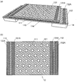
- the perspective view (a), longitudinal cross-sectional view (b), and top view (c) of the thermal radiation light source which are one Example of this invention.
- the inset is a graph showing the result of calculating the relationship between the voltage and the absorption coefficient.
- the graph which shows the result of having calculated the wavelength spectrum of the emissivity of the light in the case where a voltage is not applied between electrodes with respect to the thermal radiation light source of a present Example, and when it applies.
- the inset is a graph showing the difference between these two wavelength spectra.
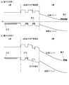
- the voltage between the electrodes is switched at a frequency of 10 kHz in the thermal radiation light source of this example (a)
- the voltage of the heater for heating the light source in the conventional thermal radiation light source as a comparative example was switched at a frequency of 10 kHz.
- the graph which shows the result of having calculated the time change of the radiation power in the case (b).
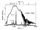
- the thermal radiation light source produced in this example the result of measuring the wavelength spectrum of the infrared rays emitted when no voltage is applied between the electrodes and when the voltage is applied can be obtained from the black body radiation light source having the same temperature and the same area.
- the data for the voltage of 8V and the data for 10V are displayed in an overlapping manner.
- the voltage between the electrodes is switched at a frequency within the range of 0.1 kHz to 1.5 MHz (100 to 1,500,000 Hz), and high-speed modulation is used to measure the temporal change in the intensity of the emitted light.
- the schematic diagram which shows the optical system of experiment.
- the graph (c) which shows the result of having measured the wavelength spectrum of emitted infrared rays.
- the perspective view (a) and top view (b) which show the modification of the thermal radiation light source which concerns on this invention.
- the thermal radiation light source 10 of this example includes a plate material 11, a hole (different refractive index region) 121, a p-type electrode 131, and an n-type electrode.
- the two-dimensional photonic crystal 12 is formed by the plate material 11 and the holes 121.
- the plate 11 is rectangular and has a structure in which a p layer 111, an i layer 113, a quantum well structure layer 114, and an n layer 112 are stacked in this order from the top.
- the thickness of each layer in this example is 800 nm for the p layer 111 and the n layer 112, and 200 nm for the i layer 113 and the quantum well structure layer 114.
- the p-layer 111 is p-GaAs, which is a p-type semiconductor in which p-type impurity Be is added to GaAs
- the n-layer 112 is an n-type impurity, in which n is an n-type impurity Si.
- N-GaAs which is a type semiconductor, and GaAs in which no impurity is implanted in the i layer 113 are used as materials.
- electron density N e of hole density N p and n layer 112 of the p layer 111 are each 1 ⁇ 10 17 cm -3.
- the quantum well structure layer 114 is formed by alternately laminating a layer made of GaAs and a layer made of n-AlGaAs. As a result, a large number of n-type quantum wells are formed in the quantum well structure layer 114 in which the portion of the layer made of GaAs is in the well.
- An energy potential in which a large number of quantum wells are formed in this way is called a multiple quantum well, and a structure having multiple quantum wells is called a multiple quantum well structure.
- the holes 121 are arranged in a triangular lattice shape within a square range in which the length L of one side of the plate 11 is 2 mm.
- the period length a of this triangular lattice is 4.8 ⁇ m.
- the two-dimensional photonic crystal 12 resonates with infrared rays having a wavelength of 9.2 ⁇ m in vacuum because the holes 121 are arranged in such a cycle.
- the hole 121 has a cylindrical shape, and the designed radius r of the cylinder is about 0.96 ⁇ m (0.20a) and the thickness is about 1.3 ⁇ m.
- the n layer 112 has a larger area than the other layers and has a portion that does not contact the quantum well structure layer 114 at both ends in the longitudinal direction.
- the n-type electrode 132 is made of a metal electrode made of Ge / Au / Ni / Au alloy that forms an ohmic junction with the n layer 112, and is provided on this portion of the n layer 112 by vapor deposition.
- the p-type electrode 131 is made of a metal electrode made of an Au / Zn / Au alloy that forms an ohmic junction with the p-layer 111, and is provided on the surface of the p-layer 111 by vapor deposition.
- the p-type electrode 131 and the n-type electrode 132 are provided at these positions, a voltage is applied between the p layer 111 and the n layer 112 with the quantum well structure layer 114 and the i layer 113 interposed therebetween. Become. Further, since the p-type electrode 131 is provided so as to surround the region (arrangement region) where the holes 121 are periodically arranged, light is extracted from the arrangement region without being blocked by the p-type electrode 131. It is.
- the legs 14 are two rectangular parallelepiped members made of insulating GaAs into which impurities are not implanted.
- the two legs 14 are attached to the lower surface of the n layer 112 in the vicinity of both ends in the longitudinal direction of the plate material 11 so as to extend in the short side direction of the plate material 11. With the legs 14, the plate member 11 is held without touching other objects except for the portion where the legs 14 are attached. Further, when the heat radiation light source 10 is heated, heat is transferred from the external heat source to the two-dimensional photonic crystal 12 through the legs 14 by heat conduction.
- the heating temperature was set to 200 ° C. for (a) the case where no voltage was applied between the p-type electrode 131 and the n-type electrode 132 and (b) the case where a voltage of 8 V was applied.
- both of (a) and (b) form a large number of quantum wells (multiple quantum wells) in the quantum well structure layer 114.
- FIG. 4 shows that both of (a) and (b) form a large number of quantum wells (multiple quantum wells) in the quantum well structure layer 114.
- the energy of the whole quantum well near the p layer 111 is higher than in the case of (a). This means that when a voltage is applied, there are no electrons in the quantum well near the p-layer 111, and fewer electrons contribute to thermal radiation than when no voltage is applied (see FIG. 1). As a result, the light absorption coefficient due to the intersubband transition (Inter Sub Band Transition: ISB-T) in the quantum well is smaller when no voltage is applied (inset in Fig. 4). ), The emission intensity is also reduced.
- ISB-T Inter Sub Band Transition
- the emissivity is defined by a value obtained by dividing the emission intensity of the thermal radiation light source 10 by the intensity of black body radiation at the same temperature at each wavelength.
- the wavelength and wave number refer to those in light in a vacuum. From this graph, it can be seen that the peak value of the emissivity at a wavelength of 9.2 ⁇ m is about 1/8 of (a) in (b).
- the ON voltage was 8 V
- the ON / OFF frequency (modulation frequency) was 10 kHz.
- the heating temperature was 200 ° C.
- infrared detector infrared rays within a certain wavelength band are detected without being distinguished by wavelength, so that the radiation power is obtained by integrating within a wavelength band of 5 to 15 ⁇ m.
- the same calculation was performed for a conventional thermal radiation light source when the input power input to the light source to change the temperature was switched at a frequency of 10 kHz.
- the difference in radiation power between the heater ON and OFF is only 0.066%.
- the modulation power is about 67%.
- FIG. 6 (a) shows a value obtained by integrating the radiation power within the wavelength band of 5 to 15 ⁇ m as described above.
- the infrared rays having a wavelength of around 9.2 ⁇ m contribute.
- the modulation power at each modulation frequency is shown in decibels as a ratio to the modulation power when the modulation frequency is low (100 Hz).
- two types of calculation are performed for the area (arrangement area) in which the holes 121 are arranged in the plate material 11 in the case of a square having a side length L of 2 mm and in the case of a square having L of 0.5 mm. It was.
- thermal radiation light source 10A (3) Results of Experiment on Thermal Radiation Light Source of the Present Example
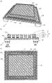
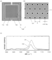
- FIG. 8 is a photomicrograph of the thermal radiation light source 10A taken from the upper side in the perspective view of FIG. In (a), the entire upper surface of the thermal radiation light source 10A was photographed with an optical microscope, and in (b), a part of the two-dimensional photonic crystal 12 was magnified and photographed with an electron microscope.
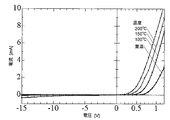
- FIG. 9 shows the results of measuring the current-voltage characteristics of the obtained thermal radiation light source 10A.
- a voltage that is positive on the p-type electrode 131 side and negative on the n-type electrode 132 side is positive. Indicated by value.
- the obtained heat radiation light source 10A was such that a current flows when the voltage is positive, and a current hardly flows when the voltage is negative. It has the characteristics as It can be said that the thermal radiation light source 10A utilizes the movement of electrons between the quantum well and the n-type semiconductor without flowing a current in the range of voltage 0 to negative bias voltage in the PIN diode.
- the voltage applied between the p-type electrode 131 and the n-type electrode 132 is (a) 0V, and (b) 10V (value expressed as negative in FIG. 9).
- the result of measuring the wavelength spectrum of the light emission intensity at a certain time is shown together with the measurement result obtained from the black body radiation light source having the same temperature and the same area.
- the light emission intensity was shown in arbitrary units, the intensity was made uniform so that comparison could be made between the measurement results of (a), (b) and the black body radiation light source. Similar to the calculation result shown in FIG.
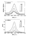
- the experimental result shows that the value of the radiant intensity of (b) is significantly smaller than that of (a) at the wavelength of 9.2 ⁇ m, while there is no light emission at other wavelengths. Or (a) and (b) indicate that light is emitted at an intensity close to each other.
- FIG. 11A the result of measuring the wavelength spectrum in the vicinity of a wavelength of 9.2 ⁇ m is shown in FIG. 11A, and the result of the calculation corresponding to this measurement is shown in FIG. , Respectively.
- the measurement result and the calculation result are in good agreement at any applied voltage.
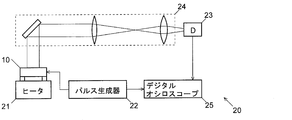
- the experimental apparatus 20 generates a pulse that generates a square-wave high-frequency voltage having a predetermined modulation frequency, which is applied between the heater 21 on which the thermal radiation light source 10 is mounted and heated, and the p-type electrode 131 and the n-type electrode 132.
- a digital oscilloscope 25 for observing the output signal by synchronizing the high-frequency voltages.
- an HgCdTe (mercury / cadmium / tellurium) detector was used as the detector 23, an HgCdTe (mercury / cadmium / tellurium) detector was used.
- the value of the high frequency voltage when the pulse generator 22 outputs ON is 10V.
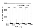
- Fig. 13 shows the measurement results when the modulation frequency is 10 kHz. A square wave output signal corresponding to the frequency of the applied voltage was obtained.
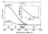
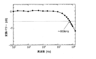
- FIG. 14 shows the result of measuring the change in modulation power according to the modulation frequency using the experimental apparatus 20.
- a modulation intensity of ⁇ 3 dB or more can be obtained. This measurement result is in good agreement with the calculation result shown in FIG.
- the carrier density will be described with reference to FIG. FIG. 15 (a)
- the emissivity when the electron density N e of hole density N p and n layer 112 of the p layer 111 is a value of the above Examples (both 1 ⁇ 10 17 cm -3)
- Left Fig. 6 is a graph showing the graph excluding the inset in Fig. 5) and the delay time tr (right diagram).
- the delay time t r refers to the time from the voltage between the electrodes is applied to actually participate in the quantum well of the photonic crystal center portion.
- the value of the voltage applied to the quantum well structure layer 114 is (1-e ⁇ 1 ) times the value after sufficient time has elapsed (e is the base of the natural logarithm, (1-e ⁇ 1 ) ⁇ 0.63) a time when that became the delay time was t r.
- the voltage between the p-type electrode 131 and the n-type electrode 132 was 8V in the left figure and 10V in the right figure.
- the delay time t r was 0.62Myuesu.
- the electron density N e of the n layer 112 remains 1 ⁇ 10 17 cm -3, and the only hole density N p of the p layer 111 is increased to 1 ⁇ 10 18 cm -3.
- the density of holes in the p layer 111 having a larger effective mass of carriers than the electrons in the n layer 112 is increased.
- FIG. 15 (c) as compared to the delay time t r with is shortened to 0.091Myuesu, changes in the emissivity of the time when the voltage OFF and ON is 0.56, the emissivity was able to be suppressed more than in the case of (b). Unnecessary radiation at wavelengths other than the target wavelength is also suppressed as compared with the case of (b).
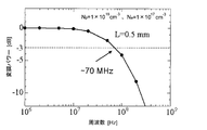
- FIG. 16 shows the result of calculation of the change in modulation power due to the modulation frequency when the hole arrangement area is a square with a side of 0.5 mm.
- the conditions in this calculation are the points where only the hole density N p of the p layer 111 is increased to 1 ⁇ 10 18 cm ⁇ 3 compared to the condition in the experiment shown in FIG. e remains 1 ⁇ 10 17 cm ⁇ 3 , that is, these carrier densities are the same as those in FIG. 15 (c)), and are different in that the area where holes are arranged is reduced.
- This calculation result shows that the upper limit frequency can be increased to about 70 MHz.
- a heat radiation light source 10B in which the radius of the hole 121 is made smaller than that of the heat radiation light source 10A of the above embodiment will be described with reference to FIG.
- the period length a of the triangular lattice is 4.5 ⁇ m
- the radius r of the air holes 121 is 0.63 ⁇ m (0.14a)
- other conditions are the same as those of the thermal radiation light source 10A.
- the micrographs of the obtained thermal radiation light source 10B are shown in FIGS. 17 (a) and 17 (b), and the results of measuring the wavelength spectrum of infrared rays emitted from the thermal radiation light source using the experimental apparatus 20 are shown in the graph. Shown in (c).
- the infrared wavelength spectrum shows the case where the applied voltage at which the radiation intensity is maximum is 2V and the case where the applied voltage at which the radiation intensity is minimum is 10V.
- the thermal radiation light source 10B when the applied voltage is 2V, the full width at half maximum of the infrared wavelength spectrum is 7.0 cm ⁇ 1 , and the full width at half maximum when the applied voltage in the thermal radiation light source 10A shown in FIG. It became narrower than 12.5cm -1 . This means that a narrower emission spectrum was obtained by reducing the hole diameter. Further, it was confirmed that when the voltage applied to the thermal radiation light source 10B was changed from 2V to 10V, the intensity of the light was lowered, and the intensity could be modulated by the voltage as in the case of the thermal radiation light source 10A.
- the present invention is not limited to the above embodiments.
- the p-layer 111, the n-layer 112, and the i-layer 113 are made of GaAs as a main constituent element, but other semiconductors may be used.
- the quantum well structure layer 114 may be made of a material other than the above. Further, the quantum well structure layer 114 is not limited to the one having an n-type quantum well, but one having a p-type quantum well, such as one in which multiple layers made of InP and layers made of p-InGaAs are alternately stacked. It may be used.
- the quantum well structure layer 114 is not limited to the one having the multiple quantum well structure in the above embodiment, and may be one having a quantum well structure in which only one quantum well is formed.
- the above thickness values of the p layer 111, the n layer 112, the i layer 113, and the quantum well structure layer 114 are merely examples, and are not limited to these values.
- the values of the hole density of the p layer 111 and the electron density of the n layer 112 (impurity density of those layers) are also examples, and are not limited to these values.
- the p layer 111 and the quantum well structure layer 114 may be directly joined without using the i layer 113.
- the holes 121 are used in the different refractive index region, but a member having a refractive index different from that of the plate 11 may be used as the different refractive index region.
- the shape and size of the different refractive index region (hole 121) are not limited to those in the above-described embodiment, and the shape may be a triangular prism shape, a quadrangular prism shape, or the like.
- the period length of the different refractive index region (holes 121) and the shape of the grating are not limited to those of the above embodiment, and a square grating or other grating may be used as the shape of the grating.
- the p-type electrode 131 is provided so as to surround the arrangement region where the holes 121 are periodically arranged. For example, as shown in FIG. Even when the p-type electrode 131A is provided, light can be extracted from the arrangement region without being blocked by the p-type electrode 131A.
- FIG. 18 like the p-type electrode 131A, two pairs of n-type electrodes 132A are used, but it is not essential to match the shapes of the p-type electrode and the n-type electrode.
- heat conduction from an external heat source is used for heating the heat radiation light source, but the heating method is not limited to this. Electric power for heating may be input to the thermal radiation light source itself, or other means may be used.
Landscapes
- Physics & Mathematics (AREA)
- Condensed Matter Physics & Semiconductors (AREA)
- General Physics & Mathematics (AREA)
- Electromagnetism (AREA)
- Optics & Photonics (AREA)
- Optical Modulation, Optical Deflection, Nonlinear Optics, Optical Demodulation, Optical Logic Elements (AREA)
- Optical Filters (AREA)
- Diffracting Gratings Or Hologram Optical Elements (AREA)
- Semiconductor Lasers (AREA)
- Photometry And Measurement Of Optical Pulse Characteristics (AREA)
Abstract
Description
a) n型半導体から成るn層、量子井戸構造を有する量子井戸構造層、及びp型半導体から成るp層がこの順で厚み方向に積層された板材内に、該量子井戸構造層における量子井戸内のサブバンド間における遷移エネルギーに対応する特定波長の光に共振するように、前記n層、前記p層及び前記量子井戸構造層とは屈折率が異なる異屈折率領域が周期的に配置された2次元フォトニック結晶と、
b) 前記p層側が負、前記n層側が正である電圧を前記板材に印加するための電極と
を備えることを特徴とする。
n型半導体から成るn層、量子井戸構造を有する量子井戸構造層、及びp型半導体から成るp層がこの順で厚み方向に積層された板材と、
前記量子井戸構造層における量子井戸内のサブバンド間における遷移エネルギーに対応する特定波長の光に共振するように、前記板材内に周期的に配置された、前記n層、前記p層及び前記量子井戸構造層とは屈折率が異なる異屈折率領域と
を備えることを特徴とする。
本実施例の熱輻射光源10は、図3に示すように、板材11、空孔(異屈折率領域)121、p型電極131、n型電極132、及び脚14を有し、板材11と空孔121により2次元フォトニック結晶12が形成されている。
次に、本実施例の熱輻射光源10の特性につき、計算によりシミュレーションを行った結果を説明する。なお、以下では、特記した場合を除いて、p型電極131とn型電極132の間に電圧を印加する際には、電圧の極性は、p層111(p型電極131)側を負、n層112(n型電極132)側を正とした。
次に、実際に作製した熱輻射光源(以下、「熱輻射光源10A」と呼ぶ)に対する実験結果を示す。図8は、熱輻射光源10Aを、図3(a)の斜視図における上側から撮影した顕微鏡写真である。(a)では熱輻射光源10Aの上面全体を光学顕微鏡で撮影し、(b)では2次元フォトニック結晶12の一部を電子顕微鏡により拡大して撮影した。
まず、キャリア密度に関して、図15を用いて説明する。図15(a)は、p層111の正孔密度Np及びn層112の電子密度Neが上記実施例の値(いずれも1×1017cm-3)である場合における放射率(左図。図5の挿入図を除くグラフの再掲。)及び遅れ時間tr(右図)を示すグラフである。ここで遅れ時間trとは、電極間に電圧が印加されてから実際にフォトニック結晶中央部の量子井戸に加わるまでの時間をいう。ここでは、量子井戸構造層114に印加された電圧の値が、十分に時間が経過した後の値の(1-e-1)倍(eは自然対数の底、(1-e-1)≒0.63)になった時の時間を遅れ時間trとした。なお、p型電極131とn型電極132間の電圧は、左図では8V、右図では10Vとした。図15(a)の計算では、電圧のOFF時とON時の間での放射率の変化は0.69、遅れ時間trは0.62μsであった。
上記実施例ではp層111、n層112及びi層113にはGaAsを主な構成元素とする半導体を用いたが、他の半導体を用いてもよい。量子井戸構造層114にも、上記以外の材料から成るものを用いてもよい。さらに、量子井戸構造層114には、n型量子井戸を有するものに限らず、InPから成る層とp-InGaAsから成る層が交互に多数積層されたもの等、p型量子井戸を有するものを用いてもよい。また、量子井戸構造層114は、上記実施例における多重量子井戸構造を有するものには限らず、量子井戸が1つのみ形成される量子井戸構造を有するものを用いてもよい。p層111、n層112、i層113及び量子井戸構造層114の上記厚みの値は一例であり、それらの値には限定されない。上記のp層111の正孔密度及びn層112の電子密度(それらの層における不純物の密度)の値も一例であり、それらの値には限定されない。また、i層113を用いることなくp層111と量子井戸構造層114を直接接合してもよい。
11…板材
111…p層
112…n層
113…i層
114…量子井戸構造層
12…2次元フォトニック結晶
121…空孔
131、131A…p型電極
132、132A…n型電極
14…脚
20…実験装置
21…ヒータ
22…パルス生成器
23…検出器
24…光学系
25…デジタルオシロスコープ
Claims (9)
- a) n型半導体から成るn層、量子井戸構造を有する量子井戸構造層、及びp型半導体から成るp層がこの順で厚み方向に積層された板材内に、該量子井戸構造層における量子井戸内のサブバンド間における遷移エネルギーに対応する特定波長の光に共振するように、前記n層、前記p層及び前記量子井戸構造層とは屈折率が異なる異屈折率領域が周期的に配置された2次元フォトニック結晶と、
b) 前記p層側が負、前記n層側が正である電圧を前記板材に印加するための電極と
を備えることを特徴とする熱輻射光源。 - 前記量子井戸構造層がn型量子井戸を有し、該量子井戸構造層と前記p層の間に絶縁体から成るi層を有することを特徴とする請求項1に記載の熱輻射光源。
- 前記量子井戸構造層がp型量子井戸を有し、該量子井戸構造層と前記n層の間に絶縁体から成るi層を有することを特徴とする請求項1に記載の熱輻射光源。
- 前記2次元フォトニック結晶が、(1/(2πRC))が目的とする周波数以上となる電気抵抗R及び電気容量Cを有することを特徴とする請求項1~3のいずれかに記載の熱輻射光源。
- 前記p層及び前記n層のうち、キャリアの有効質量が大きい方のキャリア密度が、有効質量が小さい方のキャリア密度よりも高いことを特徴とする請求項1~4のいずれかに記載の熱輻射光源。
- 前記電極が、前記p層に接し該p層を構成するp型半導体とオーミック接合となる金属製のp電極と、前記n層に接し該n層を構成するn型半導体とオーミック接合となる金属製のn電極であることを特徴とする請求項1~5のいずれかに記載の熱輻射光源。
- 前記電極が、前記板材の表面のうちの少なくとも一方に、前記異屈折率領域が周期的に配置された配置領域を囲繞するように設けられていることを特徴とする請求項1~6のいずれかに記載の熱輻射光源。
- 前記2次元フォトニック結晶を電力により加熱する加熱装置を備えることを特徴とする請求項1~7のいずれかに記載の熱輻射光源。
- 熱輻射光源に用いる2次元フォトニック結晶であって、
n型半導体から成るn層、量子井戸構造を有する量子井戸構造層、及びp型半導体から成るp層がこの順で厚み方向に積層された板材と、
前記量子井戸構造層における量子井戸内のサブバンド間における遷移エネルギーに対応する特定波長の光に共振するように、前記板材内に周期的に配置された、前記n層、前記p層及び前記量子井戸構造層とは屈折率が異なる異屈折率領域と
を備えることを特徴とする2次元フォトニック結晶。
Priority Applications (4)
| Application Number | Priority Date | Filing Date | Title |
|---|---|---|---|
| US15/120,254 US9972970B2 (en) | 2014-02-28 | 2015-02-24 | Thermal emission source and two-dimensional photonic crystal for use in the same emission source |
| JP2016505222A JP6538648B2 (ja) | 2014-02-28 | 2015-02-24 | 熱輻射光源、及び該光源に用いる2次元フォトニック結晶 |
| EP15754718.3A EP3113304B1 (en) | 2014-02-28 | 2015-02-24 | Thermal-radiation light source and two-dimensional photonic crystal used therein |
| CN201580011021.6A CN106471687B (zh) | 2014-02-28 | 2015-02-24 | 热辐射光源以及在该光源中使用的二维光子晶体 |
Applications Claiming Priority (2)
| Application Number | Priority Date | Filing Date | Title |
|---|---|---|---|
| JP2014039298 | 2014-02-28 | ||
| JP2014-039298 | 2014-02-28 |
Publications (1)
| Publication Number | Publication Date |
|---|---|
| WO2015129668A1 true WO2015129668A1 (ja) | 2015-09-03 |
Family
ID=54008986
Family Applications (1)
| Application Number | Title | Priority Date | Filing Date |
|---|---|---|---|
| PCT/JP2015/055161 WO2015129668A1 (ja) | 2014-02-28 | 2015-02-24 | 熱輻射光源、及び該光源に用いる2次元フォトニック結晶 |
Country Status (5)
| Country | Link |
|---|---|
| US (1) | US9972970B2 (ja) |
| EP (1) | EP3113304B1 (ja) |
| JP (1) | JP6538648B2 (ja) |
| CN (1) | CN106471687B (ja) |
| WO (1) | WO2015129668A1 (ja) |
Cited By (6)
| Publication number | Priority date | Publication date | Assignee | Title |
|---|---|---|---|---|
| WO2017141682A1 (ja) * | 2016-02-16 | 2017-08-24 | ローム株式会社 | 熱光変換素子および熱電変換素子 |
| WO2017150160A1 (ja) * | 2016-02-29 | 2017-09-08 | 国立大学法人京都大学 | 熱輻射光源 |
| JP2019047023A (ja) * | 2017-09-05 | 2019-03-22 | 株式会社東芝 | 面発光量子カスケードレーザ |
| JP2019091838A (ja) * | 2017-11-16 | 2019-06-13 | 株式会社東芝 | 面発光量子カスケードレーザ |
| JP2019197933A (ja) * | 2019-08-23 | 2019-11-14 | 株式会社東芝 | 面発光量子カスケードレーザ |
| US12055801B2 (en) | 2019-03-27 | 2024-08-06 | Centre National De La Recherche Scientifique | Ultra-fast modulator for modulating the amplitude of laser radiation |
Families Citing this family (2)
| Publication number | Priority date | Publication date | Assignee | Title |
|---|---|---|---|---|
| CN110400862B (zh) * | 2019-07-29 | 2021-04-02 | 中国科学院长春光学精密机械与物理研究所 | 一种红外热辐射光源及红外传感器 |
| CN111916998A (zh) * | 2020-07-13 | 2020-11-10 | 清华大学 | 基于w3光子晶体缺陷波导的分布式反馈激光器及制备方法 |
Citations (7)
| Publication number | Priority date | Publication date | Assignee | Title |
|---|---|---|---|---|
| JPS63168071A (ja) * | 1986-12-29 | 1988-07-12 | Shimadzu Corp | 半導体レ−ザ |
| JP2968255B1 (ja) * | 1998-05-28 | 1999-10-25 | 株式会社エイ・ティ・アール環境適応通信研究所 | 超格子半導体発光素子 |
| JP2005208470A (ja) * | 2004-01-26 | 2005-08-04 | Matsushita Electric Ind Co Ltd | 光変調器 |
| JP2008053134A (ja) * | 2006-08-28 | 2008-03-06 | Kyoto Univ | 2次元フォトニック結晶熱輻射光源 |
| JP2008241891A (ja) * | 2007-03-26 | 2008-10-09 | Kyoto Univ | 2次元フォトニック結晶 |
| WO2009036154A1 (en) * | 2007-09-13 | 2009-03-19 | Raytheon Company | Methods and systems for extracting energy from a heat source using photonic crystals with defect cavities |
| JP2009231773A (ja) * | 2008-03-25 | 2009-10-08 | Sumitomo Electric Ind Ltd | フォトニック結晶面発光レーザ素子およびその製造方法 |
Family Cites Families (19)
| Publication number | Priority date | Publication date | Assignee | Title |
|---|---|---|---|---|
| JPH06302906A (ja) * | 1993-04-12 | 1994-10-28 | Mitsubishi Electric Corp | 半導体レーザ及びその製造方法 |
| JPH09293405A (ja) * | 1996-04-30 | 1997-11-11 | Toshiba Lighting & Technol Corp | 反射体、白熱電球および照明器具 |
| US6583445B1 (en) * | 2000-06-16 | 2003-06-24 | Peregrine Semiconductor Corporation | Integrated electronic-optoelectronic devices and method of making the same |
| US7279718B2 (en) * | 2002-01-28 | 2007-10-09 | Philips Lumileds Lighting Company, Llc | LED including photonic crystal structure |
| CN1286228C (zh) * | 2002-02-08 | 2006-11-22 | 松下电器产业株式会社 | 半导体发光元件及其制造方法 |
| US6831302B2 (en) * | 2003-04-15 | 2004-12-14 | Luminus Devices, Inc. | Light emitting devices with improved extraction efficiency |
| JP2005045162A (ja) * | 2003-07-25 | 2005-02-17 | Mitsubishi Electric Corp | 半導体素子およびその製造方法 |
| CN100498396C (zh) * | 2006-09-29 | 2009-06-10 | 南京理工大学 | 实现热辐射光谱控制的三维层叠光子晶体 |
| JP5320566B2 (ja) * | 2007-03-26 | 2013-10-23 | 国立大学法人京都大学 | 2次元フォトニック結晶光共振器 |
| US7701629B2 (en) * | 2007-04-19 | 2010-04-20 | Hewlett-Packard Development Company, L.P. | Photonic device including semiconductor structure having doped region with array of subwavelengh recesses |
| JP5077850B2 (ja) * | 2008-08-28 | 2012-11-21 | 国立大学法人京都大学 | 2次元フォトニック結晶レーザ |
| JP5303221B2 (ja) * | 2008-08-29 | 2013-10-02 | 独立行政法人科学技術振興機構 | 2次元フォトニック結晶レーザ |
| CN101626140A (zh) * | 2009-04-17 | 2010-01-13 | 华中科技大学 | 一种垂直谐振腔超窄带红外发射光源 |
| CN102473746B (zh) * | 2009-07-23 | 2015-10-21 | 丰田自动车株式会社 | 光电转换元件 |
| JP2011054828A (ja) * | 2009-09-03 | 2011-03-17 | Kyoto Univ | フォトニック結晶発光ダイオード |
| JP2011134991A (ja) * | 2009-12-25 | 2011-07-07 | Canon Inc | フォトニック結晶発光素子 |
| TW201126853A (en) * | 2010-01-25 | 2011-08-01 | Univ Nat Changhua Education | Laser diode with asymmetric quantum well |
| CN102208461B (zh) * | 2010-03-30 | 2014-04-16 | 海洋王照明科技股份有限公司 | 太阳能电池及其制备方法 |
| US8948226B2 (en) * | 2012-08-20 | 2015-02-03 | The Board Of Trustees Of The University Of Illinois | Semiconductor device and method for producing light and laser emission |
-
2015
- 2015-02-24 WO PCT/JP2015/055161 patent/WO2015129668A1/ja active Application Filing
- 2015-02-24 JP JP2016505222A patent/JP6538648B2/ja active Active
- 2015-02-24 EP EP15754718.3A patent/EP3113304B1/en active Active
- 2015-02-24 US US15/120,254 patent/US9972970B2/en active Active
- 2015-02-24 CN CN201580011021.6A patent/CN106471687B/zh active Active
Patent Citations (7)
| Publication number | Priority date | Publication date | Assignee | Title |
|---|---|---|---|---|
| JPS63168071A (ja) * | 1986-12-29 | 1988-07-12 | Shimadzu Corp | 半導体レ−ザ |
| JP2968255B1 (ja) * | 1998-05-28 | 1999-10-25 | 株式会社エイ・ティ・アール環境適応通信研究所 | 超格子半導体発光素子 |
| JP2005208470A (ja) * | 2004-01-26 | 2005-08-04 | Matsushita Electric Ind Co Ltd | 光変調器 |
| JP2008053134A (ja) * | 2006-08-28 | 2008-03-06 | Kyoto Univ | 2次元フォトニック結晶熱輻射光源 |
| JP2008241891A (ja) * | 2007-03-26 | 2008-10-09 | Kyoto Univ | 2次元フォトニック結晶 |
| WO2009036154A1 (en) * | 2007-09-13 | 2009-03-19 | Raytheon Company | Methods and systems for extracting energy from a heat source using photonic crystals with defect cavities |
| JP2009231773A (ja) * | 2008-03-25 | 2009-10-08 | Sumitomo Electric Ind Ltd | フォトニック結晶面発光レーザ素子およびその製造方法 |
Non-Patent Citations (2)
| Title |
|---|
| DE ZOYSA, MENAKA ET AL.: "Conversion of broadband to narrowband thermal emission through energy recycling", NATURE PHOTONICS, vol. 6, no. 8, August 2012 (2012-08-01), pages 535 - 539, XP055219891, ISSN: 1749-4885 * |
| See also references of EP3113304A4 * |
Cited By (9)
| Publication number | Priority date | Publication date | Assignee | Title |
|---|---|---|---|---|
| WO2017141682A1 (ja) * | 2016-02-16 | 2017-08-24 | ローム株式会社 | 熱光変換素子および熱電変換素子 |
| WO2017150160A1 (ja) * | 2016-02-29 | 2017-09-08 | 国立大学法人京都大学 | 熱輻射光源 |
| JPWO2017150160A1 (ja) * | 2016-02-29 | 2019-01-10 | 国立大学法人京都大学 | 熱輻射光源 |
| US10777972B2 (en) | 2016-02-29 | 2020-09-15 | Kyoto University | Thermal radiation light source |
| JP2019047023A (ja) * | 2017-09-05 | 2019-03-22 | 株式会社東芝 | 面発光量子カスケードレーザ |
| JP2019091838A (ja) * | 2017-11-16 | 2019-06-13 | 株式会社東芝 | 面発光量子カスケードレーザ |
| US12055801B2 (en) | 2019-03-27 | 2024-08-06 | Centre National De La Recherche Scientifique | Ultra-fast modulator for modulating the amplitude of laser radiation |
| JP2019197933A (ja) * | 2019-08-23 | 2019-11-14 | 株式会社東芝 | 面発光量子カスケードレーザ |
| JP7076414B2 (ja) | 2019-08-23 | 2022-05-27 | 株式会社東芝 | 面発光量子カスケードレーザ |
Also Published As
| Publication number | Publication date |
|---|---|
| CN106471687B (zh) | 2019-02-19 |
| JPWO2015129668A1 (ja) | 2017-03-30 |
| US20170077675A1 (en) | 2017-03-16 |
| US9972970B2 (en) | 2018-05-15 |
| EP3113304A1 (en) | 2017-01-04 |
| CN106471687A (zh) | 2017-03-01 |
| EP3113304B1 (en) | 2022-04-13 |
| JP6538648B2 (ja) | 2019-07-03 |
| EP3113304A4 (en) | 2017-03-15 |
Similar Documents
| Publication | Publication Date | Title |
|---|---|---|
| WO2015129668A1 (ja) | 熱輻射光源、及び該光源に用いる2次元フォトニック結晶 | |
| US11231318B2 (en) | Photoconductive detector device with plasmonic electrodes | |
| US11456392B2 (en) | Metallo-graphene nanocomposites and methods for using metallo-graphene nanocomposites for electromagnetic energy conversion | |
| Lepeshov et al. | Enhancement of terahertz photoconductive antenna operation by optical nanoantennas | |
| US20170294629A1 (en) | Light emission from electrically biased graphene | |
| US20160233379A1 (en) | Terahertz source chip, source device and source assembly, and manufacturing methods thereof | |
| WO2016140946A1 (en) | Plasmon-enhanced terahertz graphene-based photodetector and method of fabrication | |
| JP5582822B2 (ja) | 電磁波発生装置 | |
| Kawazoe et al. | Bulk crystal SiC blue LED with p–n homojunction structure fabricated by dressed-photon-phonon–assisted annealing | |
| JP2011181708A (ja) | 光素子 | |
| JP6618145B2 (ja) | 熱輻射光源 | |
| EP3425754B1 (en) | Heat-radiating light source | |
| Zavvari et al. | Proposal of a quantum ring intersubband photodetector integrated with avalanche multiplication region for high performance detection of far infrared | |
| RU2536327C2 (ru) | Генератор субтерагерцового и терагерцового излучения на основе оптического транзистора | |
| Berry et al. | High-performance photoconductive terahertz sources based on nanoscale contact electrode gratings | |
| RU2431225C1 (ru) | Полупроводниковый частотно-перестраиваемый источник инфракрасного излучения | |
| Inoue et al. | Electrical wavelength switching of thermal emitters based on quantum wells and photonic crystals | |
| JP6829517B2 (ja) | 赤外光素子 | |
| Ohtsu et al. | Energy Conversion Using Dressed Photons | |
| Das | Effect of grating on IR LED device performance | |
| Inoue et al. | Dynamic control of narrowband thermal emission | |
| Klaassen et al. | Negative photoconductivity due to coherent trapping of electrons in n-GaAs | |
| Yardimci et al. | Large Area Plasmonic Photoconductive Emitters for Generating High Power Broadband Terahertz Radiation | |
| Yusefli | Proposal of a quantum ring intersubband photodetector |
Legal Events
| Date | Code | Title | Description |
|---|---|---|---|
| 121 | Ep: the epo has been informed by wipo that ep was designated in this application |
Ref document number: 15754718 Country of ref document: EP Kind code of ref document: A1 |
|
| ENP | Entry into the national phase |
Ref document number: 2016505222 Country of ref document: JP Kind code of ref document: A |
|
| WWE | Wipo information: entry into national phase |
Ref document number: 15120254 Country of ref document: US |
|
| REEP | Request for entry into the european phase |
Ref document number: 2015754718 Country of ref document: EP |
|
| WWE | Wipo information: entry into national phase |
Ref document number: 2015754718 Country of ref document: EP |
|
| NENP | Non-entry into the national phase |
Ref country code: DE |