WO2015125199A1 - 表示装置およびその駆動方法 - Google Patents
表示装置およびその駆動方法 Download PDFInfo
- Publication number
- WO2015125199A1 WO2015125199A1 PCT/JP2014/006423 JP2014006423W WO2015125199A1 WO 2015125199 A1 WO2015125199 A1 WO 2015125199A1 JP 2014006423 W JP2014006423 W JP 2014006423W WO 2015125199 A1 WO2015125199 A1 WO 2015125199A1
- Authority
- WO
- WIPO (PCT)
- Prior art keywords
- signal
- driver
- pixel circuits
- cascade
- display device
- Prior art date
- Legal status (The legal status is an assumption and is not a legal conclusion. Google has not performed a legal analysis and makes no representation as to the accuracy of the status listed.)
- Ceased
Links
Images




Classifications
-
- G—PHYSICS
- G09—EDUCATION; CRYPTOGRAPHY; DISPLAY; ADVERTISING; SEALS
- G09G—ARRANGEMENTS OR CIRCUITS FOR CONTROL OF INDICATING DEVICES USING STATIC MEANS TO PRESENT VARIABLE INFORMATION
- G09G3/00—Control arrangements or circuits, of interest only in connection with visual indicators other than cathode-ray tubes
- G09G3/006—Electronic inspection or testing of displays and display drivers, e.g. of LED or LCD displays
-
- G—PHYSICS
- G09—EDUCATION; CRYPTOGRAPHY; DISPLAY; ADVERTISING; SEALS
- G09G—ARRANGEMENTS OR CIRCUITS FOR CONTROL OF INDICATING DEVICES USING STATIC MEANS TO PRESENT VARIABLE INFORMATION
- G09G3/00—Control arrangements or circuits, of interest only in connection with visual indicators other than cathode-ray tubes
- G09G3/20—Control arrangements or circuits, of interest only in connection with visual indicators other than cathode-ray tubes for presentation of an assembly of a number of characters, e.g. a page, by composing the assembly by combination of individual elements arranged in a matrix no fixed position being assigned to or needed to be assigned to the individual characters or partial characters
- G09G3/2085—Special arrangements for addressing the individual elements of the matrix, other than by driving respective rows and columns in combination
-
- G—PHYSICS
- G09—EDUCATION; CRYPTOGRAPHY; DISPLAY; ADVERTISING; SEALS
- G09G—ARRANGEMENTS OR CIRCUITS FOR CONTROL OF INDICATING DEVICES USING STATIC MEANS TO PRESENT VARIABLE INFORMATION
- G09G3/00—Control arrangements or circuits, of interest only in connection with visual indicators other than cathode-ray tubes
- G09G3/20—Control arrangements or circuits, of interest only in connection with visual indicators other than cathode-ray tubes for presentation of an assembly of a number of characters, e.g. a page, by composing the assembly by combination of individual elements arranged in a matrix no fixed position being assigned to or needed to be assigned to the individual characters or partial characters
- G09G3/22—Control arrangements or circuits, of interest only in connection with visual indicators other than cathode-ray tubes for presentation of an assembly of a number of characters, e.g. a page, by composing the assembly by combination of individual elements arranged in a matrix no fixed position being assigned to or needed to be assigned to the individual characters or partial characters using controlled light sources
- G09G3/30—Control arrangements or circuits, of interest only in connection with visual indicators other than cathode-ray tubes for presentation of an assembly of a number of characters, e.g. a page, by composing the assembly by combination of individual elements arranged in a matrix no fixed position being assigned to or needed to be assigned to the individual characters or partial characters using controlled light sources using electroluminescent panels
- G09G3/32—Control arrangements or circuits, of interest only in connection with visual indicators other than cathode-ray tubes for presentation of an assembly of a number of characters, e.g. a page, by composing the assembly by combination of individual elements arranged in a matrix no fixed position being assigned to or needed to be assigned to the individual characters or partial characters using controlled light sources using electroluminescent panels semiconductive, e.g. using light-emitting diodes [LED]
- G09G3/3208—Control arrangements or circuits, of interest only in connection with visual indicators other than cathode-ray tubes for presentation of an assembly of a number of characters, e.g. a page, by composing the assembly by combination of individual elements arranged in a matrix no fixed position being assigned to or needed to be assigned to the individual characters or partial characters using controlled light sources using electroluminescent panels semiconductive, e.g. using light-emitting diodes [LED] organic, e.g. using organic light-emitting diodes [OLED]
- G09G3/3225—Control arrangements or circuits, of interest only in connection with visual indicators other than cathode-ray tubes for presentation of an assembly of a number of characters, e.g. a page, by composing the assembly by combination of individual elements arranged in a matrix no fixed position being assigned to or needed to be assigned to the individual characters or partial characters using controlled light sources using electroluminescent panels semiconductive, e.g. using light-emitting diodes [LED] organic, e.g. using organic light-emitting diodes [OLED] using an active matrix
- G09G3/3233—Control arrangements or circuits, of interest only in connection with visual indicators other than cathode-ray tubes for presentation of an assembly of a number of characters, e.g. a page, by composing the assembly by combination of individual elements arranged in a matrix no fixed position being assigned to or needed to be assigned to the individual characters or partial characters using controlled light sources using electroluminescent panels semiconductive, e.g. using light-emitting diodes [LED] organic, e.g. using organic light-emitting diodes [OLED] using an active matrix with pixel circuitry controlling the current through the light-emitting element
-
- G—PHYSICS
- G09—EDUCATION; CRYPTOGRAPHY; DISPLAY; ADVERTISING; SEALS
- G09G—ARRANGEMENTS OR CIRCUITS FOR CONTROL OF INDICATING DEVICES USING STATIC MEANS TO PRESENT VARIABLE INFORMATION
- G09G3/00—Control arrangements or circuits, of interest only in connection with visual indicators other than cathode-ray tubes
- G09G3/20—Control arrangements or circuits, of interest only in connection with visual indicators other than cathode-ray tubes for presentation of an assembly of a number of characters, e.g. a page, by composing the assembly by combination of individual elements arranged in a matrix no fixed position being assigned to or needed to be assigned to the individual characters or partial characters
- G09G3/22—Control arrangements or circuits, of interest only in connection with visual indicators other than cathode-ray tubes for presentation of an assembly of a number of characters, e.g. a page, by composing the assembly by combination of individual elements arranged in a matrix no fixed position being assigned to or needed to be assigned to the individual characters or partial characters using controlled light sources
- G09G3/30—Control arrangements or circuits, of interest only in connection with visual indicators other than cathode-ray tubes for presentation of an assembly of a number of characters, e.g. a page, by composing the assembly by combination of individual elements arranged in a matrix no fixed position being assigned to or needed to be assigned to the individual characters or partial characters using controlled light sources using electroluminescent panels
- G09G3/32—Control arrangements or circuits, of interest only in connection with visual indicators other than cathode-ray tubes for presentation of an assembly of a number of characters, e.g. a page, by composing the assembly by combination of individual elements arranged in a matrix no fixed position being assigned to or needed to be assigned to the individual characters or partial characters using controlled light sources using electroluminescent panels semiconductive, e.g. using light-emitting diodes [LED]
- G09G3/3208—Control arrangements or circuits, of interest only in connection with visual indicators other than cathode-ray tubes for presentation of an assembly of a number of characters, e.g. a page, by composing the assembly by combination of individual elements arranged in a matrix no fixed position being assigned to or needed to be assigned to the individual characters or partial characters using controlled light sources using electroluminescent panels semiconductive, e.g. using light-emitting diodes [LED] organic, e.g. using organic light-emitting diodes [OLED]
- G09G3/3225—Control arrangements or circuits, of interest only in connection with visual indicators other than cathode-ray tubes for presentation of an assembly of a number of characters, e.g. a page, by composing the assembly by combination of individual elements arranged in a matrix no fixed position being assigned to or needed to be assigned to the individual characters or partial characters using controlled light sources using electroluminescent panels semiconductive, e.g. using light-emitting diodes [LED] organic, e.g. using organic light-emitting diodes [OLED] using an active matrix
- G09G3/3233—Control arrangements or circuits, of interest only in connection with visual indicators other than cathode-ray tubes for presentation of an assembly of a number of characters, e.g. a page, by composing the assembly by combination of individual elements arranged in a matrix no fixed position being assigned to or needed to be assigned to the individual characters or partial characters using controlled light sources using electroluminescent panels semiconductive, e.g. using light-emitting diodes [LED] organic, e.g. using organic light-emitting diodes [OLED] using an active matrix with pixel circuitry controlling the current through the light-emitting element
- G09G3/3241—Control arrangements or circuits, of interest only in connection with visual indicators other than cathode-ray tubes for presentation of an assembly of a number of characters, e.g. a page, by composing the assembly by combination of individual elements arranged in a matrix no fixed position being assigned to or needed to be assigned to the individual characters or partial characters using controlled light sources using electroluminescent panels semiconductive, e.g. using light-emitting diodes [LED] organic, e.g. using organic light-emitting diodes [OLED] using an active matrix with pixel circuitry controlling the current through the light-emitting element the current through the light-emitting element being set using a data current provided by the data driver, e.g. by using a two-transistor current mirror
- G09G3/325—Control arrangements or circuits, of interest only in connection with visual indicators other than cathode-ray tubes for presentation of an assembly of a number of characters, e.g. a page, by composing the assembly by combination of individual elements arranged in a matrix no fixed position being assigned to or needed to be assigned to the individual characters or partial characters using controlled light sources using electroluminescent panels semiconductive, e.g. using light-emitting diodes [LED] organic, e.g. using organic light-emitting diodes [OLED] using an active matrix with pixel circuitry controlling the current through the light-emitting element the current through the light-emitting element being set using a data current provided by the data driver, e.g. by using a two-transistor current mirror the data current flowing through the driving transistor during a setting phase, e.g. by using a switch for connecting the driving transistor to the data driver
-
- G—PHYSICS
- G09—EDUCATION; CRYPTOGRAPHY; DISPLAY; ADVERTISING; SEALS
- G09G—ARRANGEMENTS OR CIRCUITS FOR CONTROL OF INDICATING DEVICES USING STATIC MEANS TO PRESENT VARIABLE INFORMATION
- G09G3/00—Control arrangements or circuits, of interest only in connection with visual indicators other than cathode-ray tubes
- G09G3/20—Control arrangements or circuits, of interest only in connection with visual indicators other than cathode-ray tubes for presentation of an assembly of a number of characters, e.g. a page, by composing the assembly by combination of individual elements arranged in a matrix no fixed position being assigned to or needed to be assigned to the individual characters or partial characters
- G09G3/22—Control arrangements or circuits, of interest only in connection with visual indicators other than cathode-ray tubes for presentation of an assembly of a number of characters, e.g. a page, by composing the assembly by combination of individual elements arranged in a matrix no fixed position being assigned to or needed to be assigned to the individual characters or partial characters using controlled light sources
- G09G3/30—Control arrangements or circuits, of interest only in connection with visual indicators other than cathode-ray tubes for presentation of an assembly of a number of characters, e.g. a page, by composing the assembly by combination of individual elements arranged in a matrix no fixed position being assigned to or needed to be assigned to the individual characters or partial characters using controlled light sources using electroluminescent panels
- G09G3/32—Control arrangements or circuits, of interest only in connection with visual indicators other than cathode-ray tubes for presentation of an assembly of a number of characters, e.g. a page, by composing the assembly by combination of individual elements arranged in a matrix no fixed position being assigned to or needed to be assigned to the individual characters or partial characters using controlled light sources using electroluminescent panels semiconductive, e.g. using light-emitting diodes [LED]
- G09G3/3208—Control arrangements or circuits, of interest only in connection with visual indicators other than cathode-ray tubes for presentation of an assembly of a number of characters, e.g. a page, by composing the assembly by combination of individual elements arranged in a matrix no fixed position being assigned to or needed to be assigned to the individual characters or partial characters using controlled light sources using electroluminescent panels semiconductive, e.g. using light-emitting diodes [LED] organic, e.g. using organic light-emitting diodes [OLED]
- G09G3/3266—Details of drivers for scan electrodes
-
- G—PHYSICS
- G11—INFORMATION STORAGE
- G11C—STATIC STORES
- G11C19/00—Digital stores in which the information is moved stepwise, e.g. shift registers
-
- H—ELECTRICITY
- H10—SEMICONDUCTOR DEVICES; ELECTRIC SOLID-STATE DEVICES NOT OTHERWISE PROVIDED FOR
- H10K—ORGANIC ELECTRIC SOLID-STATE DEVICES
- H10K59/00—Integrated devices, or assemblies of multiple devices, comprising at least one organic light-emitting element covered by group H10K50/00
- H10K59/10—OLED displays
- H10K59/12—Active-matrix OLED [AMOLED] displays
-
- G—PHYSICS
- G09—EDUCATION; CRYPTOGRAPHY; DISPLAY; ADVERTISING; SEALS
- G09G—ARRANGEMENTS OR CIRCUITS FOR CONTROL OF INDICATING DEVICES USING STATIC MEANS TO PRESENT VARIABLE INFORMATION
- G09G2300/00—Aspects of the constitution of display devices
- G09G2300/04—Structural and physical details of display devices
- G09G2300/0421—Structural details of the set of electrodes
- G09G2300/0426—Layout of electrodes and connections
-
- G—PHYSICS
- G09—EDUCATION; CRYPTOGRAPHY; DISPLAY; ADVERTISING; SEALS
- G09G—ARRANGEMENTS OR CIRCUITS FOR CONTROL OF INDICATING DEVICES USING STATIC MEANS TO PRESENT VARIABLE INFORMATION
- G09G2300/00—Aspects of the constitution of display devices
- G09G2300/04—Structural and physical details of display devices
- G09G2300/0421—Structural details of the set of electrodes
- G09G2300/043—Compensation electrodes or other additional electrodes in matrix displays related to distortions or compensation signals, e.g. for modifying TFT threshold voltage in column driver
-
- G—PHYSICS
- G09—EDUCATION; CRYPTOGRAPHY; DISPLAY; ADVERTISING; SEALS
- G09G—ARRANGEMENTS OR CIRCUITS FOR CONTROL OF INDICATING DEVICES USING STATIC MEANS TO PRESENT VARIABLE INFORMATION
- G09G2300/00—Aspects of the constitution of display devices
- G09G2300/08—Active matrix structure, i.e. with use of active elements, inclusive of non-linear two terminal elements, in the pixels together with light emitting or modulating elements
- G09G2300/0809—Several active elements per pixel in active matrix panels
- G09G2300/0819—Several active elements per pixel in active matrix panels used for counteracting undesired variations, e.g. feedback or autozeroing
-
- G—PHYSICS
- G09—EDUCATION; CRYPTOGRAPHY; DISPLAY; ADVERTISING; SEALS
- G09G—ARRANGEMENTS OR CIRCUITS FOR CONTROL OF INDICATING DEVICES USING STATIC MEANS TO PRESENT VARIABLE INFORMATION
- G09G2300/00—Aspects of the constitution of display devices
- G09G2300/08—Active matrix structure, i.e. with use of active elements, inclusive of non-linear two terminal elements, in the pixels together with light emitting or modulating elements
- G09G2300/0809—Several active elements per pixel in active matrix panels
- G09G2300/0842—Several active elements per pixel in active matrix panels forming a memory circuit, e.g. a dynamic memory with one capacitor
-
- G—PHYSICS
- G09—EDUCATION; CRYPTOGRAPHY; DISPLAY; ADVERTISING; SEALS
- G09G—ARRANGEMENTS OR CIRCUITS FOR CONTROL OF INDICATING DEVICES USING STATIC MEANS TO PRESENT VARIABLE INFORMATION
- G09G2300/00—Aspects of the constitution of display devices
- G09G2300/08—Active matrix structure, i.e. with use of active elements, inclusive of non-linear two terminal elements, in the pixels together with light emitting or modulating elements
- G09G2300/0809—Several active elements per pixel in active matrix panels
- G09G2300/0842—Several active elements per pixel in active matrix panels forming a memory circuit, e.g. a dynamic memory with one capacitor
- G09G2300/0861—Several active elements per pixel in active matrix panels forming a memory circuit, e.g. a dynamic memory with one capacitor with additional control of the display period without amending the charge stored in a pixel memory, e.g. by means of additional select electrodes
-
- G—PHYSICS
- G09—EDUCATION; CRYPTOGRAPHY; DISPLAY; ADVERTISING; SEALS
- G09G—ARRANGEMENTS OR CIRCUITS FOR CONTROL OF INDICATING DEVICES USING STATIC MEANS TO PRESENT VARIABLE INFORMATION
- G09G2310/00—Command of the display device
- G09G2310/02—Addressing, scanning or driving the display screen or processing steps related thereto
- G09G2310/0264—Details of driving circuits
- G09G2310/0286—Details of a shift registers arranged for use in a driving circuit
-
- G—PHYSICS
- G09—EDUCATION; CRYPTOGRAPHY; DISPLAY; ADVERTISING; SEALS
- G09G—ARRANGEMENTS OR CIRCUITS FOR CONTROL OF INDICATING DEVICES USING STATIC MEANS TO PRESENT VARIABLE INFORMATION
- G09G2320/00—Control of display operating conditions
- G09G2320/06—Adjustment of display parameters
- G09G2320/0626—Adjustment of display parameters for control of overall brightness
- G09G2320/0646—Modulation of illumination source brightness and image signal correlated to each other
-
- G—PHYSICS
- G09—EDUCATION; CRYPTOGRAPHY; DISPLAY; ADVERTISING; SEALS
- G09G—ARRANGEMENTS OR CIRCUITS FOR CONTROL OF INDICATING DEVICES USING STATIC MEANS TO PRESENT VARIABLE INFORMATION
- G09G2330/00—Aspects of power supply; Aspects of display protection and defect management
- G09G2330/04—Display protection
-
- G—PHYSICS
- G09—EDUCATION; CRYPTOGRAPHY; DISPLAY; ADVERTISING; SEALS
- G09G—ARRANGEMENTS OR CIRCUITS FOR CONTROL OF INDICATING DEVICES USING STATIC MEANS TO PRESENT VARIABLE INFORMATION
- G09G2330/00—Aspects of power supply; Aspects of display protection and defect management
- G09G2330/04—Display protection
- G09G2330/045—Protection against panel overheating
-
- G—PHYSICS
- G09—EDUCATION; CRYPTOGRAPHY; DISPLAY; ADVERTISING; SEALS
- G09G—ARRANGEMENTS OR CIRCUITS FOR CONTROL OF INDICATING DEVICES USING STATIC MEANS TO PRESENT VARIABLE INFORMATION
- G09G2330/00—Aspects of power supply; Aspects of display protection and defect management
- G09G2330/08—Fault-tolerant or redundant circuits, or circuits in which repair of defects is prepared
-
- G—PHYSICS
- G09—EDUCATION; CRYPTOGRAPHY; DISPLAY; ADVERTISING; SEALS
- G09G—ARRANGEMENTS OR CIRCUITS FOR CONTROL OF INDICATING DEVICES USING STATIC MEANS TO PRESENT VARIABLE INFORMATION
- G09G2330/00—Aspects of power supply; Aspects of display protection and defect management
- G09G2330/10—Dealing with defective pixels
-
- G—PHYSICS
- G09—EDUCATION; CRYPTOGRAPHY; DISPLAY; ADVERTISING; SEALS
- G09G—ARRANGEMENTS OR CIRCUITS FOR CONTROL OF INDICATING DEVICES USING STATIC MEANS TO PRESENT VARIABLE INFORMATION
- G09G2330/00—Aspects of power supply; Aspects of display protection and defect management
- G09G2330/12—Test circuits or failure detection circuits included in a display system, as permanent part thereof
-
- H—ELECTRICITY
- H10—SEMICONDUCTOR DEVICES; ELECTRIC SOLID-STATE DEVICES NOT OTHERWISE PROVIDED FOR
- H10K—ORGANIC ELECTRIC SOLID-STATE DEVICES
- H10K59/00—Integrated devices, or assemblies of multiple devices, comprising at least one organic light-emitting element covered by group H10K50/00
- H10K59/10—OLED displays
-
- H—ELECTRICITY
- H10—SEMICONDUCTOR DEVICES; ELECTRIC SOLID-STATE DEVICES NOT OTHERWISE PROVIDED FOR
- H10K—ORGANIC ELECTRIC SOLID-STATE DEVICES
- H10K59/00—Integrated devices, or assemblies of multiple devices, comprising at least one organic light-emitting element covered by group H10K50/00
- H10K59/10—OLED displays
- H10K59/12—Active-matrix OLED [AMOLED] displays
- H10K59/131—Interconnections, e.g. wiring lines or terminals
Definitions
- the present disclosure relates to a display device, and more particularly, to a display device using a light emitting element that emits light according to an electric current and a driving method thereof.
- ACF is a material formed in a tape shape by mixing conductive particles with an adhesive.
- the ACF is sandwiched between the terminals of different substrates and thermocompression bonded to electrically connect the terminals in the vertical direction via the conductive particles and at the same time insulate the terminals on the same substrate. Then, the substrates are bonded together by curing the adhesive.
- Such an ACF connection can be used as an alternative to the connection by a connector, and enables connection with a multi-pin, low profile and narrow pitch compared to the connector.
- both ends of the COF substrate are thermocompression bonded and ACF connection is made between the printed circuit board and the COF substrate, and the COF substrate and the display panel substrate, it is difficult to obtain a high connection strength.
- the COF substrate is flexible, it has a certain degree of rigidity. Therefore, for example, when the COF substrate is repeatedly distorted due to thermal expansion or contraction of each substrate, the end portion of the COF substrate that has been thermocompression bonded may be peeled off by the strain stress.
- Patent Document 1 discloses a technique for preventing the film end portion of the COF substrate from being peeled off from the printed circuit board or the liquid crystal display panel. That is, by providing an opening in the COF substrate, the rigidity of the COF film is weakened, the flexibility is increased, the strain stress is reduced, and peeling is prevented.
- the present disclosure provides a display device that detects peeling between a COF substrate and a printed circuit board, and a driving method thereof.
- a display device includes a display panel substrate having a plurality of pixel circuits arranged in a matrix, a plurality of film substrates connected to the display panel substrate, and the display panel substrate or A driver IC for display driving having a shift register, mounted on the film substrate, a printed circuit board having a wiring connected to the plurality of film substrates and cascading the driver ICs, and the most upstream of the cascade connection A control unit that supplies a predetermined signal to the cascade input terminal of the driver IC that is positioned, and monitors the signal of the cascade output terminal of at least one driver IC that is positioned downstream of the driver IC that is positioned on the most upstream side.
- the display device in the present disclosure it is possible to detect peeling between the COF substrate and the printed circuit board.
- FIG. 1 is a block diagram illustrating a configuration example of a display device and a pixel circuit in Embodiment 1.
- FIG. 2 is a diagram illustrating a configuration example of various substrates and wirings of the display device according to the first embodiment and a more detailed configuration example of the control unit.
- 3A is a diagram illustrating an example of mounting various substrates in the display device in Embodiment 1.
- FIG. 3B is a cross-sectional view showing a BB cross section in FIG. 3A.
- 4A is a development view of a mounting example of a substrate constituting the display device in Embodiment 1.
- FIG. 4B is an enlarged view of a portion A in FIG. 4A.
- FIG. 5 is an enlarged view of a portion C in FIG. FIG.
- FIG. 6A is a flowchart showing the operation of the control unit.
- FIG. 6B is a flowchart illustrating the operation of the control unit.
- FIG. 7 is a diagram illustrating a configuration example of various substrates and wirings of the display device according to the second embodiment.
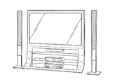
- FIG. 8 is a diagram illustrating a product example of the display device.
- FIG. 1 is a block diagram illustrating a configuration example of a display device and a pixel circuit in Embodiment 1.
- the display device 1 in FIG. 1 includes a display panel substrate 20, gate drive circuits 12a and 12b, a source drive circuit 14, a control unit 30, and a panel power supply unit 32.
- the display panel substrate 20 includes a plurality of pixel circuits 16 arranged in a matrix.
- the plurality of pixel circuits 16 are formed on the display panel substrate 20 by a semiconductor process.
- the material of the display panel substrate 20 is a resin such as glass or acrylic.
- the plurality of pixel circuits 16 are arranged in n rows and m columns. n and m differ depending on the size and resolution of the display unit. For example, when the pixel circuit 16 corresponding to the RGB three primary colors is adjacent in a row at a resolution called HD (High Definition), n is at least 1080 rows and m is at least 1920 ⁇ 3 columns.
- HD High Definition
- Each pixel circuit 16 constitutes a light emitting pixel of any of the three primary colors RGB.
- the pixel circuit 16 includes a light emitting element 41, a drive transistor 42, an enable switch 43, a scan switch 44, a capacitive element 45, a REF switch 46, and an INI switch 47.
- the pixel circuits 16 belonging to the i-th (i is an integer from 1 to n) -th row are connected to the ENB (i) signal line, the REF (i) signal line, the INI (i) signal line, and the SCN (i) signal line. Connected. To these signal lines, an enable signal, a REF control signal, an INI control signal, and a scan signal are supplied from the gate drive circuits 12a and 12b.
- the pixel circuit 16 belonging to the jth column (j is an integer from 1 to m) is connected to the D (j) signal line.
- a voltage corresponding to the luminance to be emitted is supplied from the source drive circuit 14 to the D (j) signal line.
- the ENB (i) signal line transmits an enable signal for controlling light emission and non-light emission of the pixel circuits 16 belonging to the i-th row.
- the enable signal controls ON / OFF of the enable switch 43 in the corresponding pixel circuit 16.
- the SCN (i) signal line transmits a scan signal (also referred to as a write signal) that controls writing of pixel data to the pixel circuits 16 belonging to the i-th row.
- the scan signal controls on / off of the scan switch 44 in the corresponding pixel circuit 16.
- the REF (i) signal line transmits a REF control signal for controlling the supply of the reference voltage to the pixel circuits 16 belonging to the i-th row.
- This REF control signal controls on / off of the REF switch 46 in the corresponding pixel circuit 16.
- the INI (i) signal line transmits an INI control signal for controlling the supply of the initialization voltage to the pixel circuits 16 belonging to the i-th row.
- This INI control signal controls ON / OFF of the INI switch 47 in the corresponding pixel circuit 16.
- the D (j) signal line is a data line that transmits a voltage representing the brightness of the pixel as pixel data to the pixel circuit 16 belonging to the jth column. This pixel data is supplied from the D (j) signal line to the capacitive element 45 via the scan switch 44 under the control of the scan signal.
- the light emitting element 41 is an organic EL element, which is an example of a light emitting element called OLED (Organic Light Emitting Diode), and emits light with brightness according to the magnitude of the current flowing through it.
- OLED Organic Light Emitting Diode
- the anode of the light emitting element 41 is connected to the source of the driving transistor 42, and the cathode of the light emitting element 41 is connected to the power supply line VEL.
- the drive transistor 42 is a driver that supplies current to the light emitting element 41.
- the gate of the drive transistor 42 is connected to one electrode of the capacitive element 45, and the source is connected to the other electrode of the capacitive element 45 and the anode of the light emitting element 41.
- a voltage held in the capacitive element 45 that is, a voltage representing the brightness of the pixel is applied between the gate and the source of the driving transistor 42. Accordingly, the drive transistor 42 supplies the light emitting element 41 with an amount of current corresponding to the voltage of the capacitor 45.
- the enable switch 43 is a switch transistor that turns on and off the current supply to the light emitting element 41 by the driving transistor 42.
- the enable switch 43 is turned on and off according to the enable signal.
- the enable signal enables and disables light emission of the pixel circuit 16 for each row of the plurality of pixel circuits 16 in a matrix. That is, when the ENB signal line is at a high level, the enable switch 43 is in an on state and supplies the voltage VTFT to the drive transistor 42. In addition, when the enable signal line is at a low level, the enable switch 43 is in an off state and cuts off the supply of the voltage VTFT to the drive transistor 42.
- the scan switch 44 is a switch transistor for writing a voltage representing the brightness of the pixel to the capacitive element 45 as pixel data.
- the scan signal is a write signal for selecting a plurality of pixel circuits 16 in a matrix form in units of rows and writing a voltage representing luminance to the pixel circuits 16 belonging to the selected row. That is, when the SCN signal line is at a high level, the scan switch 44 is in an on state, and the voltage of the data line is written into the capacitor 45 as pixel data. When the SCN signal line is at a low level, the scan switch 44 is off, and the connection between the scan signal line and the capacitor 45 is electrically cut off.
- the capacitive element 45 holds a voltage representing the brightness of the pixel between the gate and source of the driving transistor 42 as pixel data.
- the REF switch 46 is a switch transistor for applying a reference voltage VREF to one electrode of the capacitive element 45.
- the INI switch 47 is a switch transistor for applying the initialization voltage VINI to the other electrode of the capacitive element 45.
- the REF switch 46 and the INI switch 47 are used for a threshold compensation operation in which the capacitor 45 holds a voltage corresponding to the actual threshold voltage of the drive transistor 42 to which the capacitor 45 is connected. More specifically, the threshold compensation operation refers to an operation for compensating for a threshold shift of a driving transistor in a plurality of pixel circuits.
- the maximum threshold voltage (that is, the maximum value when a threshold value shift occurs) in the capacitive element 45. Voltage). Further, by passing a current through the driving transistor 42 while the light emitting element 41 is not emitting light, the set initial voltage is lowered to a voltage corresponding to the actual threshold voltage of the driving transistor 42. Up to here is the threshold voltage compensation operation. Thereby, the capacitive element 45 holds a voltage corresponding to the actual threshold voltage of the corresponding drive transistor 42. In this state, writing is performed so that the voltage of pixel data is added to the capacitive element 45.
- the threshold voltage compensation operation is an operation for compensating for a variation in threshold value due to a threshold shift as a change with time between the pixel circuits 16, and every time pixel data is written to the capacitive element 45. It is executed immediately before that.
- the display panel substrate 20 shown in FIG. 1 has a circuit configuration as described above.
- the gate drive circuits 12a and 12b drive the same gate signal to the display panel substrate 20 at the same timing. This is to suppress signal deterioration due to the wiring capacity of each signal line in a large display device. In a small display device, only one gate driving circuit 12 is required.
- the gate signal is a signal input to the gate of each switch transistor in the pixel circuit 16.
- the gate signal there are four types of gate signals: an enable signal, a REF control signal, an INI control signal, and a scan signal.
- the gate drive circuit 12a controls the ENB (1) signal line to ENB (n) signal line, SCN (i) signal line to SCN (n) signal line, REF (1) signal line to REF ( n)
- the signal line, INI (1) signal line to INI (n) signal line is scanned.
- the gate drive circuit 12a outputs an enable signal, a scan signal, a REF control signal, and an INI control signal for each row of the pixel circuit.
- the gate drive circuit 12b has the same configuration as the gate drive circuit 12a, and outputs the same signal as the gate drive circuit 12a at the same timing.
- the source drive circuit 14 supplies a voltage representing the brightness of the pixels belonging to each column to the D (1) signal line to the D (m) signal line based on the video signal input from the control unit 30. That is, a voltage representing the brightness of each pixel is supplied from the D (1) signal line to the D (m) signal line. The supplied voltage is written into the pixel circuit 16 belonging to the row selected by the scan signal line.
- the video signal input from the control unit 30 to the source drive circuit 14 is input as digital serial data for each of the three primary colors of RGB, for example, converted into parallel data in units of rows within the source drive circuit 14, and Converted to analog data in units.
- a large display device may be provided with two source driving circuits on the upper and lower sides and output the same signal at the same timing.
- the control unit 30 controls the operation of the entire display device.
- the control unit 30 instructs the gate driving circuits 12a and 12b to start scanning in accordance with the vertical synchronizing signal and horizontal synchronizing signal of the video signal from the outside, and supplies the digital serial data to the source driving circuit 14. To do.
- the panel power supply unit 32 supplies various voltages to each pixel circuit 16 of the display panel substrate 20.
- the various voltages referred to here are VTFT, VEL, VREF, and VINI in the pixel circuit example shown in FIG.
- the panel power supply unit 32 can turn on and off the supply of the voltages under the control of the control unit 30.
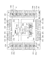
- FIG. 2 is a diagram showing a configuration example of various substrates and wirings of the display device according to the first embodiment and a more detailed configuration example of the control unit.
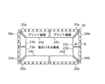
- FIG. 3A is a diagram showing an example of mounting various substrates in the display device in Embodiment 1.
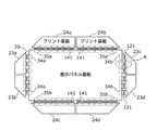
- FIG. 4A is a development view of a mounting example of various boards shown in FIG. 3A.
- FIG. 3A, and FIG. 4A represent the back surface opposite to the display surface of the display device 1 of FIG.
- the left-right arrangement relationship is not reversed with respect to FIG. That is, the left side of these figures corresponds to the left side of FIG. 1, and the right side of these figures corresponds to the right side of FIG.
- the display device 1 includes a display panel substrate 20, printed circuit boards 23a to 23d and 24a to 24d, a plurality of COF substrates 34a, 34b, 35a and 35b, and a control unit. 30 and a panel power supply unit 32.
- the control unit 30 includes a TCON 95, a microcomputer 31, and a control signal generation unit 33.
- the control unit 30 is mounted on one of the printed boards 23a to 23d, the printed boards 24a to 24d, or another printed board.
- the panel power supply part 32 is mounted on another printed circuit board.
- FIG. 1 the correspondence between FIG. 1 and FIGS. 2, 3A and 4A will be described.
- 1 corresponds to a plurality of COF boards 34a, printed boards 23a, and printed boards 23b arranged on the left side of the display panel board 20 in FIGS. 2, 3A, and 4A.
- FIGS. 2, 3A, and 3B corresponds to the plurality of COF substrates 34b, the printed circuit board 23c, and the printed circuit board 23d arranged on the right side of the display panel substrate 20 in FIGS. 2, 3A, and 3B.
- 1 corresponds to a plurality of COF boards 35a, printed boards 24a, and printed boards 24b arranged on the upper side 20 of FIGS. 2, 3A, and 3B.
- FIG. 1 shows only one source driving circuit 14 on the upper side of the display panel substrate 20, in FIGS. 2, 3A, and 4A, the source driving circuit 14 is connected to the upper side of the display panel substrate 20. The case where two are provided on the lower side is illustrated.
- the plurality of COF substrates 35b, the printed circuit board 24c, and the printed circuit board 24d arranged on the lower side of the display panel substrate 20 correspond to another source driving circuit (that is, the lower side that is not shown in FIG. 1).
- the COF substrates 34a and 34b are simply expressed as the COF substrate 34.
- the COF substrates 35a and 35b are similarly expressed as the COF substrate 35.
- the printed boards 23a to 23d and the printed boards 24a to 24d are referred to as a printed board 23 and a printed board 24, respectively.
- the display panel substrate 20 has a plurality of pixel circuits 16 arranged in a matrix as shown in FIG.
- the display panel substrate 20 is connected to a plurality of COF substrates 34a, 34b, 35a, 35b at the outer periphery of the display surface.
- the COF substrate 34 is a film substrate on which a display driving gate driver IC 121 having a shift register is mounted.
- the display panel substrate 20 and the printed circuit board 23 or 24 are interposed for connection.
- FIG. 3B is a sectional view showing a BB section in FIG. 3A.
- the COF substrate 34 and the printed circuit board 23c are thermocompression bonded with an ACF (Anisotropic Conductive Film) interposed therebetween, so that the terminals (that is, the pads of the display panel substrate 20) are interposed between the conductive particles in the ACF.
- the pads of the COF substrate 34 are electrically connected to each other and the terminals in the same substrate are insulated and bonded by curing the adhesive.
- a connection point 39 in a broken circle in FIG. 3B is a connection point by ACF between one pad of the COF substrate 34 and one pad of the display panel substrate 20.
- COF substrate 34 and the display panel substrate 20 are similarly joined by thermocompression bonding with the ACF interposed therebetween.
- FIG. 4B is an enlarged view of a portion A in FIG. 4A.
- the COF substrate 34 is a film substrate on which the gate driver IC 121 is mounted. Pad rows are formed on both sides of the COF substrate 34 across the gate driver IC 121.
- the pad row on the display panel substrate 20 side of the COF substrate 34 is connected to the gate signal output terminal of the gate driver IC 121 by wiring.
- the pad row connected to the gate signal terminal is connected to the above-described ENB (i) signal line, SCN (i) signal line, REF (i) signal line, and INI (i) signal line of the display panel substrate 20. Connected through.
- the pad row on the printed circuit board 23 side of the COF substrate 34 is wired to a cascade input terminal for cascade connection, a cascade output terminal, a clock signal input terminal, and the like of the gate driver IC 121.
- This bad row is connected to the printed circuit board 23 via a connection point 39.
- the cascade connection of the gate driver IC 121 means that the shift register in the gate driver IC 121 and the shift register in the gate driver IC 121 of the adjacent COF substrate 34 are connected in series.
- FIG. 5 is an enlarged view of a portion C in FIG.
- the gate driver IC 121 includes four shift registers 122 for scanning and driving the four signals to the display panel substrate 20 as gate signals.
- Each of the shift registers 122 includes a shift register circuit composed of K FFs (Flip Flop) connected in series, and an output that drives the output signal of each stage of the shift register circuit to the outside as a gate signal by increasing the drive capability of the output signal. And a buffer.
- Each of the shift registers 122 is a shift register of K (for example, K is 180) stages, and has a cascade input terminal Ci, a cascade output terminal Co, and K gate signal output terminals o1 to oK as shown in FIG. .
- the original signal of the enable signal is input from the TCON 95 through the gate signal line 94b (FIG. 2) to the leftmost shift register 122 cascade input terminal Ci in FIG.
- the shift register 122 performs a shift operation in synchronization with the clock signal. For example, an enable signal is output from the gate signal output terminal o1 corresponding to the first-stage FF at the first rising edge of the clock signal. Shift operation is performed. By this shift operation, the row of the pixel circuits 16 on the display panel substrate 20 is scanned.
- an enable signal is output from the gate signal output terminal oK corresponding to the K-th stage FF at the rising edge of the K-th clock of the clock signal.
- the cascade output terminal Co outputs the same signal as the gate signal output terminal oK.
- the cascade output terminal Co is connected to the cascade input terminal Ci of the leftmost shift register 122 of the COF board 34b adjacent to the downstream side of the cascade connection via the connection point 39, the wiring on the printed circuit board 23 and the other connection point 39. Is input.
- the printed circuit board 23 has wiring that cascade-connects the leftmost shift register 122 in the gate driver IC 121 of the plurality of COF substrates 34b.
- K is 180 and the number of display rows is 1080
- six gate driver ICs 121 are cascade-connected.
- the leftmost shift register 122 of each of the six gate driver ICs 121 is cascade-connected (here, the same as the series connection), and functions as one long shift register. That is, the gate signal output terminals (o1 to oK) ⁇ 6 of the leftmost shift register 122 in the six gate driver ICs 121 scan the ENB (1) signal line to ENB (n) for the enable signal.
- the cascade output terminal of the gate driver IC 121 located at the most downstream position of the cascade connection is connected to the TCON 95 via the return signal line 96b as shown in FIG.
- the TCON 95 can detect an abnormality in wiring connection such as peeling.
- the return signal lines 96a and 96b only need to be connected to the cascade output terminal of at least one driver IC located downstream from the driver IC located upstream of the cascade connection.
- the enable signal is cascade-connected in the plurality of gate driver ICs 121 as described above.
- the second shift register 122 from the left in the six gate driver ICs 121 is the same except that it corresponds to the REF control signal.
- the third shift register 122 from the left in the six gate driver ICs 121 is the same except that it corresponds to the INI control signal.
- the fourth shift register 122 from the left in the six gate driver ICs 121 is the same except that it corresponds to the scan signal.
- the gate drive circuit 12a is the same as the gate drive circuit 12b. That is, each of the plurality (for example, six) of COF substrates 34a is connected to the display panel substrate 20 and mounted with a display driving gate driver IC 121 having a shift register.
- the printed boards 23a and 23b are connected to these COF boards 34a and have wirings that cascade-connect the gate driver ICs 121.
- the control unit 30 supplies a gate signal to the cascade input terminal of the gate driver IC 121 located at the most upstream of the cascade connection via the gate signal line 94a, and returns the signal at the cascade output terminal of the gate driver IC 121 located at the most downstream. Monitoring is performed via the signal line 96a.
- control unit 30 Next, the configuration of the control unit 30 will be described.
- the TCON 95 in the control unit 30 receives a predetermined signal (for example, via the gate signal line 94a) to the cascade input terminal of the gate driver IC 121 located in the uppermost stream of the cascade connection in the plurality of COF substrates 34a in the gate drive circuit 12a.
- Gate signal and the signal at the cascade output terminal of the gate driver IC 121 located on the most downstream side is monitored via the return signal line 96a.
- the TCON 95 supplies a predetermined signal to the cascade input terminal of the gate driver IC 121 located at the most upstream of the cascade connection in the plurality of COF substrates 34b via the gate signal line 94b.
- a gate signal is supplied, and the signal at the cascade output terminal of the gate driver IC 121 located on the most downstream side is monitored via the return signal line 96b.
- the microcomputer 31 When the microcomputer 31 receives the monitoring result of the TCON 95 and an abnormality is detected, the microcomputer 31 stops the gate signal, stops the power supply from the panel power supply unit 32 to the display panel substrate 20, and the like.
- the control signal generation unit 33 generates various control signals for controlling each unit of the display device 1 (for example, a tuner, a signal reception unit from a remote controller, an audio signal output unit, etc.).
- control unit 30 may not monitor the signal of the cascade output terminal to be monitored from the gate driver IC 121 located at the most downstream side.
- the signal may be a signal at the cascade output terminal of all the gate driver ICs 121 connected in cascade, or may be the cascade output terminal of the gate driver IC 121 at an intermediate position in the cascade connection. That is, the control unit 30 only needs to monitor the signal at the cascade output terminal of at least one gate driver IC located downstream from the gate driver IC located upstream.
- FIG. 6A is a flowchart example showing the above operation by the TCON 95 in the control unit 30.
- the TCON 95 sets a normal code in a register in the TCON 95 (S60).
- This register may be one of general-purpose registers in the TCON 95 or a dedicated register.
- the setting of the normal code is initialization of the register, and may be executed only once, for example, when the display device 1 is activated. If the normal code is determined to be all bits 0, for example, it can also be used for register clear in the initialization operation.
- the TCON 95 supplies a gate signal or a test signal to the gate signal line 94a and the gate signal line 94b at the same timing (S62). Simultaneously with or prior to the supply of the gate signal or test signal, a clock signal for shift operation is also supplied to the gate drive circuits 12a and 12b.
- the gate signal is an enable signal, a REF control signal, an INI control signal, and four scan signals, and the gate signal may be output in a normal display operation. Further, a test signal having a specific signal pattern may be output during a period when the normal display operation is not performed.
- the period during which the normal display operation is not performed may be, for example, when the display device 1 is activated, a video signal switching period (for example, a channel switching period, a video input source switching period), or the like.
- the test signal pattern may be the same signal pattern as the gate signal in normal display, a signal pattern with a constant period such as a clock signal, or a specific signal pattern.
- the panel power supply unit 32 may be controlled to stop automatically.
- the TCON 95 waits for a certain period of time from the output of the gate signal or the test signal (S64). This fixed period is the time until the gate signal or test signal appears on the return signal lines 96a and 96b through the shift operation of the gate drive circuits 12a and 12b. Specifically, (the total shift of the gate drive circuit 12) This is a time corresponding to (number of stages) ⁇ (one period of the shift clock signal).
- the TCON 95 receives signals from the return signal lines 96a and 96b (S66). Further, the TCON 95 compares the signal pattern of the transmitted gate signal or test signal with the received signal pattern (S68). The TCON 95 determines that it is normal if it matches (S70: Yes) and terminates the processing. If it does not match (S70: No), it determines that it is abnormal and sets an abnormal code in the register (S72).
- the abnormality code may be, for example, 8 bits including 4 bits corresponding to the four signals on the return signal line 96a and 4 bits corresponding to the four signals on the return signal line 96b. Each bit may take a value of 0 if normal and 1 if abnormal. In this way, the abnormal code can indicate which of the gate drive circuit 12a and the gate drive circuit 12b is abnormal and which of the four signal lines is abnormal.
- the TCON 95 can detect an abnormality in wiring connection such as peeling of the COF substrate 34, and can further indicate the detected abnormality by an abnormality code.
- FIG. 6B is a flowchart showing an operation example by the control of the microcomputer 31 in the control unit 30.
- the microcomputer 31 polls the register in the TCON 95 (S74). That is, the microcomputer 31 reads out the register periodically or when a predetermined event occurs. Further, the microcomputer 31 determines whether or not the read data is normal (S76). The microcomputer 31 ends this process when the determination result is normal. Further, when the determination result is abnormal, the microcomputer 31 prohibits the output of the enable signal thereafter, that is, to enable and disable the light emission of the pixel circuit 16 for each row of the plurality of pixel circuits 16. The TCON 95 is instructed to fix the enable signal to a level indicating disable (S78). Further, the microcomputer 31 controls the panel power supply unit 32 so as to stop the power supply to the power supply line that supplies the voltage VTFT to the plurality of pixel circuits 16 (S80).
- control unit 30 can prevent abnormal display, abnormal heat generation, breakage, and the like of the display device due to the gate signal not being properly supplied when an abnormality in wiring connection such as peeling occurs.
- the microcomputer 31 may perform the following (1) to (5) instead of the above steps S78 and S80.
- the microcomputer 31 sets the level of the enable signal to Instructs TCON 95 to fix to a level indicating disable.
- a gate signal determined to be abnormal is a write signal (that is, a scan signal) for selecting a plurality of pixel circuits 16 in units of rows and writing a voltage representing luminance to the pixel circuits 16 belonging to the selected row.
- the microcomputer 31 controls the panel power supply unit 32 so as to stop power supply to the power supply line that supplies power to the plurality of pixel circuits 16.
- a gate signal determined to be abnormal is a write signal (that is, a scan signal) for selecting a plurality of pixel circuits 16 in units of rows and writing a voltage that expresses luminance to the pixel circuits 16 belonging to the selected row.
- the microcomputer 31 fixes the level of the enable signal for enabling and disabling the light emission of the pixel circuit 16 for each row of the plurality of pixel circuits 16 to a level indicating disable.
- the gate signal determined to be abnormal is selected by selecting the enable signal for enabling and disabling the light emission of the pixel circuit for each row of the plurality of pixel circuits 16 and the plurality of pixel circuits 16 in units of rows.
- a write signal (that is, a scan signal) for writing a voltage representing luminance to the pixel circuits 16 belonging to the row, and a reference voltage setting signal (that is, a REF control signal) that applies a reference voltage to the pixel circuit 16 for each row of the plurality of pixel circuits 16.
- an initial voltage setting signal that is, an INI control signal
- the microcomputer 31 disables the level of the enable signal.
- the panel power supply is fixed so that the power supply to the power supply line that supplies the voltage VTFT to the plurality of pixel circuits 16 is stopped. Controlling the section 32.
- the microcomputer 31 enables the enable signal, the enable signal, and the write signal.
- the panel power supply unit 32 is controlled to stop power supply to each.
- an abnormality in wiring connection such as peeling between the COF substrate 34 and the printed circuit board 23 can be detected, and details of the detected abnormality can be indicated by an abnormality code. Furthermore, when a wiring connection abnormality such as peeling occurs, it is possible to prevent an abnormal display, abnormal heat generation, damage, etc. of the display device due to the gate signal not being supplied appropriately.
- the return signal line 96b may connect the cascade output terminal of at least one of the gate driver ICs 121 connected in cascade to the TCON 95.
- the return signal line 96b may connect each of the cascade output terminals of all the gate driver ICs 121 from the most upstream to the most downstream to the TCON 95.
- the cascade output terminals of the plurality of gate driver ICs 121 selected from the cascade-connected gate driver ICs 121 may be connected to the TCON 95.
- the microcomputer 31 can detect in more detail which gate driver IC 121 of the cascade-connected gate driver ICs 121 is normal and which gate driver IC 121 is abnormal. . In this way, for example, if the microcomputer 31 can detect that only one of the most upstream is normal and the downstream is abnormal, K microcomputers corresponding to the most upstream gate driver IC 121 are detected. A message informing the user of an abnormality can be displayed for the pixel circuit rows.
- the present invention is not limited to this and is similar to the above.
- the TCON 95 may generate an interrupt signal to the microcomputer 31 in S72.
- the microcomputer 31 can omit S74 and S76 and execute S78 and S80 as interrupt processing.
- Embodiment 2 Next, the display device in Embodiment 2 will be described.
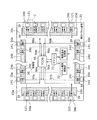
- FIG. 7 is a diagram showing a configuration example of various substrates and wirings of the display device in this embodiment. This figure is different from FIG. 2 in that data signal lines 97a and 97b and return signal lines 98a and 98b are added. Hereinafter, different points will be mainly described.
- the data signal lines 97a and 97b are signal lines that are not shown in FIG. 2, and are pixel data included in a video signal from a tuner in the display device or from the outside and to be supplied to the pixel circuit.
- This data signal line 97a is connected to the cascade input terminal of the COF substrate 35a located at the head of the display column.
- the source driver ICs 141 in the plurality of COF substrates 35a are cascade-connected. That is, the cascade output terminals of the source driver ICs 141 in the plurality of COF substrates 35a are connected to the cascade input terminals of the source driver ICs 141 in the adjacent downstream COF substrate 35a via the printed circuit board 24.
- Each of the source driver ICs 141 includes, for example, a shift register, a latch circuit that latches pixel data output in parallel from the shift register, and m that converts pixel data of the latch circuit into an analog value (m is the number of columns of the pixel circuit)
- a plurality of digital-analog converters and an output buffer for outputting analog values output from the digital-analog converters to the D (1) signal line to the D (m) signal line.
- the return signal line 98a is connected to the TCON 95 from the cascade output terminal of the source driver IC 141 in the COF substrate 35a located on the most downstream side of the cascade connection, and feeds back pixel data to the TCON 95.
- the TCON 95 detects a wiring connection abnormality such as peeling of the COF substrate 35a by monitoring the signal of the return signal line 98a.
- the detected abnormality is written in the register as an abnormality code indicating a connection abnormality of the COF board 35a.
- This register may be the same as the register described in FIG. 6A or may be a different register.
- the microcomputer 31 polls the register, and when an abnormal code is set, the level of the enable signal is fixed to a level indicating disable or a power supply line for supplying power to the plurality of pixel circuits 16
- the power supply unit is controlled so as to stop the power supply to.
- the display device not only detects connection abnormality such as peeling of the COF substrate 34 on which the source driver IC 141 is mounted, but also causes connection abnormality such as peeling of the COF substrate 35 on which the source driver IC 141 is mounted. Can be detected.
- connection abnormality such as peeling of the COF substrate 34 on which the source driver IC 141 is mounted
- connection abnormality such as peeling of the COF substrate 35 on which the source driver IC 141 is mounted.
- a wiring connection abnormality such as peeling occurs, it is possible to prevent an abnormal display, abnormal heat generation, breakage, or the like of the display device due to an inadequate supply of a gate signal or a data signal.
- the return signal line 98a may connect the cascade output terminal of at least one of the source driver ICs 141 connected in cascade with the TCON 95.
- the return signal line 98a may connect each of the cascade output terminals of all the source driver ICs 141 from the most upstream to the most downstream and the TCON 95.
- the cascade output terminals of the plurality of source driver ICs 141 selected from the cascade-connected source driver ICs 141 may be connected to the TCON 95.
- the microcomputer 31 can detect in more detail which source driver IC 141 of the cascade-connected source driver IC 141 is normal and which source driver IC 141 is abnormal. .
- K microcomputers corresponding to one source driver IC 141 of the most upstream are detected.
- a message informing the user of an abnormality can be displayed for the pixel circuit rows.
- the present invention is not limited to this and is the same as described above.
- the TCON 95 compares the signals on the return signal lines 96a, 96b, 98a, and 98b with the original signals output by the TCON 95 on the gate signal lines 94a and 94b and the data signal lines 97a and 97b. Therefore, the wiring abnormality such as peeling is determined.
- the present invention is not limited to this.
- the TCON 95 may determine whether the signal is normal or abnormal depending on whether or not the signals of the return signal lines 96a, 96b, 98a, and 98b are changing.
- each signal of the return signal lines 96a, 96b, 98a, 98b is determined to be normal if there is a change in signal level in a period of one frame period or more in normal display, and is determined to be abnormal if there is no change. Also good.
- the return signal lines 96a and 96b are not limited to the gate signals described above, but may be signals transmitted by cascade connection of the gate driver IC 121.
- a clock signal for shift operation supplied to the gate driver IC 121 may be used.
- the return signal lines 98a and 968 are not limited to the data signals described above, but may be signals transmitted by cascade connection of the source driver IC 141.
- a clock signal for shift operation supplied to the source driver IC 141 may be used.
- a display device includes a display panel substrate having a plurality of pixel circuits arranged in a matrix, a plurality of film substrates connected to the display panel substrate, A driver IC for display driving having a shift register, mounted on the display panel substrate or the film substrate, a printed circuit board connected to the plurality of film substrates and having wiring for cascading the driver ICs, and the cascade connection For supplying a predetermined signal to the cascade input terminal of the driver IC located at the most upstream side of the driver IC and monitoring the signal at the cascade output terminal of at least one driver IC located downstream from the driver IC located at the most upstream side A part.
- the driver IC is, for example, the gate driver IC 121 or the source driver IC 141.
- the film substrate is, for example, a COF substrate 34a, 34b or a COF substrate 35a, 35b.
- connection abnormality such as peeling of the film substrate can be detected.
- control unit may compare the predetermined signal with the signal of the cascade output terminal, and may determine that an abnormality occurs if they do not match.
- the predetermined signal is an enable signal for enabling and disabling light emission of the pixel circuit for each row of the plurality of pixel circuits, and when the control unit determines that there is an abnormality, The power supply unit may be controlled to stop power supply to a power supply line that supplies power to the pixel circuit.
- the predetermined signal is an enable signal for enabling and disabling light emission of the pixel circuit for each row of the plurality of pixel circuits, and when the control unit determines that there is an abnormality, the enable signal The level may be fixed to a level indicating disable.
- the predetermined signal is a write signal for selecting the plurality of pixel circuits in units of rows, and writing a voltage representing luminance to the pixel circuits belonging to the selected row, and the control section
- the power supply unit may be controlled to stop power supply to a power supply line that supplies power to the plurality of pixel circuits.
- the predetermined signal is a write signal that is selected in units of rows of the plurality of pixel circuits and writes a voltage representing luminance to the pixel circuits belonging to the selected row, and the control unit
- the level of the enable signal for enabling and disabling the light emission of the pixel circuit for each row of the plurality of pixel circuits may be fixed to a level indicating disable.
- the predetermined signal belongs to a selected row selected for each row of the plurality of pixel circuits, an enable signal for enabling and disabling light emission of the pixel circuits for each row of the plurality of pixel circuits.
- a write signal for writing a voltage representing luminance to the pixel circuit a reference voltage setting signal for applying a reference voltage to the pixel circuit for each row of the plurality of pixel circuits, and an initial value for the pixel circuit for each row of the plurality of pixel circuits
- the power supply unit may be controlled to stop power supply to a power supply line that supplies power to the plurality of pixel circuits.
- the predetermined signal is a signal representing pixel data to be supplied to one of the plurality of pixel circuits, and when the control unit determines that there is an abnormality, the row of the plurality of pixel circuits.
- the level of the enable signal for enabling and disabling the light emission of the pixel circuit is fixed to a level indicating disable or the power supply to the power supply line that supplies power to the plurality of pixel circuits is stopped. In this way, the power supply unit may be controlled.
- the printed circuit board includes a wiring for cascading the driver ICs of the film substrate corresponding to the one side and a wiring for cascading the driver ICs of the film substrate corresponding to the other side, and the control unit
- the same predetermined signal is applied to the cascade input terminal of the most upstream driver IC among the driver ICs corresponding to the one side and the cascade input terminal of the most upstream driver IC among the driver ICs corresponding to the other side at the same timing.
- the cascade output terminal of the driver IC downstream of the most upstream driver IC corresponding to the one side and the other side A respective signal cascade output terminal of the downstream side of the driver IC may be monitored than the most upstream of the driver IC to be.
- a display device driving method includes a display panel substrate having a plurality of pixel circuits arranged in a matrix, a plurality of film substrates connected to the display panel substrate, and the display panel substrate.
- a display device driving method comprising: a driver IC for display driving having a shift register mounted on the film substrate; and a printed circuit board having a wiring connected to the plurality of film substrates and cascading the driver ICs.
- connection abnormality such as peeling of the film substrate can be detected.
- the display device and the driving method thereof have been described based on the embodiment, but the present disclosure is not limited to this embodiment.
- the technology in the present disclosure is not limited to these, and can also be applied to embodiments in which changes, replacements, additions, omissions, and the like have been made as appropriate.
- various modifications conceived by those skilled in the art have been made in this embodiment, and forms constructed by combining components in different embodiments are also within the scope of one or more aspects. Contained within.
- the driver IC is mounted on the display panel substrate as well as the configuration using the film substrate in which the driver IC is mounted on the film (COF configuration), and the driver IC is mounted on the film substrate. May not be mounted (COG (Chip On Glass) configuration).
- the display device described above can be used as a flat panel display device as shown in FIG. 8, for example.
- the present invention can be applied to all electronic devices having a display device such as a television receiver, a personal computer, and a mobile phone.
- the display panel described above is not limited to an organic EL display device, and may be a flat panel display device such as a liquid crystal display device or a PDP (Plasma Display Panel) display device.
- a flat panel display device such as a liquid crystal display device or a PDP (Plasma Display Panel) display device.
- the present disclosure can be used for a display device such as a television receiver or a display of an information device.
Landscapes
- Engineering & Computer Science (AREA)
- Physics & Mathematics (AREA)
- Computer Hardware Design (AREA)
- General Physics & Mathematics (AREA)
- Theoretical Computer Science (AREA)
- Microelectronics & Electronic Packaging (AREA)
- Control Of Indicators Other Than Cathode Ray Tubes (AREA)
- Devices For Indicating Variable Information By Combining Individual Elements (AREA)
- Control Of El Displays (AREA)
- Electroluminescent Light Sources (AREA)
Abstract
Description
以下、適宜図面を参照しながら、実施の形態を詳細に説明する。但し、必要以上に詳細な説明は省略する場合がある。例えば、既によく知られた事項の詳細説明や実質的に同一の構成に対する重複説明を省略する場合がある。これは、以下の説明が不必要に冗長になるのを避け、当業者の理解を容易にするためである。また、各図は、必ずしも各寸法あるいは各寸法比等を厳密に図示したものではない。
図1は、実施の形態1における表示装置および画素回路の構成例を示すブロック図である。同図の表示装置1は、表示パネル基板20、ゲート駆動回路12a、12b、ソース駆動回路14、制御部30、パネル電源供給部32を備える。
まず、表示パネル基板20の回路構成例について説明する。
次に、表示パネル基板20周辺の構成について説明する。
続いて、表示装置を構成する各種基板および配線の構成例と制御部の構成について説明する。
ゲートドライバIC121の接続についてさらに図5を用いて詳細に説明する。図5は、図2におけるC部の拡大図である。
以上のように構成された表示装置における、COF基板34の剥離を検出する動作例を説明する。この動作例は、主に制御部30内のTCON95およびマイコン31によりなされる。
本実施の形態における表示装置によれば、COF基板34とプリント基板23との間の剥離等の配線接続の異常を検出することができ、検出した異常の詳細を異常コードにより示すことができる。さらに、剥離等の配線接続の異常が発生したときに、ゲート信号が適切に供給されないことに起因する表示装置の異常表示、異常発熱および破損等を防止することができる。
次に、実施の形態2における表示装置について説明する。
12、12a、12b ゲート駆動回路
14 ソース駆動回路
16 画素回路
20 表示パネル基板
23、23a~23d プリント基板
24、24a~24d プリント基板
30 制御部
31 マイコン
32 パネル電源供給部
33 制御信号生成部
34、34a、34b COF基板
35、35a、35b COF基板
39 接続箇所
41 発光素子
42 駆動トランジスタ
43 イネーブルスイッチ
44 スキャンスイッチ
45 容量素子45
46 REFスイッチ
47 INIスイッチ
94a、94b ゲート信号線
95 TCON95
96a、96b 戻り信号線
97a、97b データ信号線
98a、98b 戻り信号線
121 ゲートドライバIC
122 シフトレジスタ
141 ソースドライバIC
Ci カスケード入力端子
Co カスケード出力端子
o1~oK ゲート信号出力端子
Claims (10)
- 行列状に配置された複数の画素回路を有する表示パネル基板と、
前記表示パネル基板に接続された複数のフィルム基板と、
前記表示パネル基板または前記フィルム基板に実装された、シフトレジスタを有する表示駆動用のドライバICと、
前記複数のフィルム基板に接続され、前記ドライバICをカスケード接続する配線を有するプリント基板と、
前記カスケード接続の最上流に位置するドライバICのカスケード入力端子に所定の信号を供給し、前記最上流に位置するドライバICよりも下流側に位置する少なくとも1つのドライバICのカスケード出力端子の信号を監視する制御部と
を備える表示装置。 - 前記制御部は、前記所定の信号と前記カスケード出力端子の信号とを比較し、一致しない場合は異常と判定する
請求項1に記載の表示装置。 - 前記所定の信号は、前記複数の画素回路の行毎に画素回路の発光をイネーブルおよびディスエーブルするためのイネーブル信号であり、
前記制御部は、異常と判定されたとき、前記複数の画素回路に電源を供給する電源線への電力供給を停止するように電源供給部を制御する
請求項2に記載の表示装置。 - 前記所定の信号は、前記複数の画素回路の行毎に画素回路の発光をイネーブルおよびディスエーブルするためのイネーブル信号であり、
前記制御部は、異常と判定されたとき、前記イネーブル信号のレベルを、ディスエーブルを示すレベルに固定する
請求項2に記載の表示装置。 - 前記所定の信号は、前記複数の画素回路を行単位に選択し、選択された行に属する画素回路に輝度を表す電圧を書き込むための書き込み信号であり、
前記制御部は、異常と判定されたとき、前記複数の画素回路に電源を供給する電源線への電力供給を停止するように電源供給部を制御する
請求項2に記載の表示装置。 - 前記所定の信号は、前記複数の画素回路の行単位に選択し、選択された行に属する画素回路に輝度を表す電圧を書き込むための書き込み信号であり、
前記制御部は、異常と判定されたとき、前記複数の画素回路の行毎に画素回路の発光をイネーブルおよびディスエーブルするためのイネーブル信号のレベルを、ディスエーブルを示すレベルに固定する
請求項2に記載の表示装置。 - 前記所定の信号は、前記複数の画素回路の行毎に画素回路の発光をイネーブルおよびディスエーブルするためのイネーブル信号、前記複数の画素回路の行単位に選択し選択された行に属する画素回路に輝度を表す電圧を書き込むための書き込み信号、前記複数の画素回路の行毎に画素回路に基準電圧を与える基準電圧設定信号、および、前記複数の画素回路の行毎に画素回路に初期電圧を与える初期電圧設定信号を含み、
前記制御部は、前記所定の信号の何れかが異常であると判定されたとき、前記イネーブル信号のレベルを、ディスエーブルを示すレベルに固定し、または、前記複数の画素回路に電源を供給する電源線への電力供給を停止するように電源供給部を制御する
請求項2に記載の表示装置。 - 前記所定の信号は、前記複数の画素回路の1つに供給すべき画素データを表す信号であり、
前記制御部は、異常であると判定されたとき、前記複数の画素回路の行毎に画素回路の発光をイネーブルおよびディスエーブルするためのイネーブル信号のレベルを、ディスエーブルを示すレベルに固定し、または、前記複数の画素回路に電源を供給する電源線への電力供給を停止するように電源供給部を制御する
請求項2に記載の表示装置。 - 前記複数のフィルム基板の一部は、前記表示パネル基板の一辺の表面側に接続され、前記複数のフィルム基板の他の一部は、前記一辺に対向する他辺の表面側に接続され、
前記プリント基板は、前記一辺に対応するフィルム基板の前記ドライバICをカスケード接続する配線と、前記他辺に対応するフィルム基板の前記ドライバICをカスケード接続する配線とを有し、
前記制御部は、
前記一辺に対応するドライバICのうち最上流のドライバICのカスケード入力端子、および、前記他辺に対応するドライバICのうち最上流のドライバICのカスケード入力端子に同じ所定の信号を同じタイミングで供給し、
前記一辺に対応する最上流のドライバICよりも下流側のドライバICのカスケード出力端子、および、前記他辺に対応する最上流のドライバICよりも下流側のドライバICのカスケード出力端子のそれぞれの信号を監視する
請求項1~7のいずれか1項に記載の表示装置。 - 行列状に配置された複数の画素回路を有する表示パネル基板と、
前記表示パネル基板に接続された複数のフィルム基板と、
前記表示パネル基板または前記フィルム基板に実装された、シフトレジスタを有する表示駆動用のドライバICと、
前記複数のフィルム基板に接続され、前記ドライバICをカスケード接続する配線を有するプリント基板と
を備える表示装置の駆動方法であって、
前記カスケード接続の最上流に位置するドライバICのカスケード入力端子に所定の信号を供給するステップと、
前記最上流に位置するドライバICよりも下流側に位置する少なくとも1つのドライバICのカスケード出力端子の信号を監視するステップと
を有する表示装置の駆動方法。
Priority Applications (2)
| Application Number | Priority Date | Filing Date | Title |
|---|---|---|---|
| JP2016503797A JP6311171B2 (ja) | 2014-02-19 | 2014-12-24 | 表示装置 |
| US15/118,256 US9892667B2 (en) | 2014-02-19 | 2014-12-24 | Display device and method for driving same |
Applications Claiming Priority (2)
| Application Number | Priority Date | Filing Date | Title |
|---|---|---|---|
| JP2014029728 | 2014-02-19 | ||
| JP2014-029728 | 2014-02-19 |
Publications (1)
| Publication Number | Publication Date |
|---|---|
| WO2015125199A1 true WO2015125199A1 (ja) | 2015-08-27 |
Family
ID=53877740
Family Applications (1)
| Application Number | Title | Priority Date | Filing Date |
|---|---|---|---|
| PCT/JP2014/006423 Ceased WO2015125199A1 (ja) | 2014-02-19 | 2014-12-24 | 表示装置およびその駆動方法 |
Country Status (3)
| Country | Link |
|---|---|
| US (1) | US9892667B2 (ja) |
| JP (1) | JP6311171B2 (ja) |
| WO (1) | WO2015125199A1 (ja) |
Cited By (7)
| Publication number | Priority date | Publication date | Assignee | Title |
|---|---|---|---|---|
| JPWO2017033844A1 (ja) * | 2015-08-27 | 2018-06-28 | シャープ株式会社 | 表示装置およびその電源制御方法 |
| CN109243347A (zh) * | 2018-10-31 | 2019-01-18 | 合肥鑫晟光电科技有限公司 | 栅极驱动器的检测电路及显示装置 |
| JP2019128470A (ja) * | 2018-01-25 | 2019-08-01 | セイコーエプソン株式会社 | 電気光学装置、および電子機器 |
| JP2020024316A (ja) * | 2018-08-08 | 2020-02-13 | 株式会社Joled | 表示装置及び表示装置の検査方法 |
| JP2020115173A (ja) * | 2019-01-17 | 2020-07-30 | シャープ株式会社 | 表示装置 |
| JP2021001943A (ja) * | 2019-06-20 | 2021-01-07 | 株式会社ジャパンディスプレイ | 液晶表示装置 |
| CN115047662A (zh) * | 2015-08-31 | 2022-09-13 | 乐金显示有限公司 | 透明显示设备及其制造方法 |
Families Citing this family (6)
| Publication number | Priority date | Publication date | Assignee | Title |
|---|---|---|---|---|
| KR102705336B1 (ko) * | 2016-10-06 | 2024-09-12 | 삼성디스플레이 주식회사 | 표시 장치 |
| JP6917806B2 (ja) * | 2017-06-30 | 2021-08-11 | 株式会社ジャパンディスプレイ | 表示装置 |
| CN113674714B (zh) * | 2021-08-23 | 2023-04-21 | 京东方科技集团股份有限公司 | 驱动电路板、显示模组及其制作方法、显示装置 |
| CN115035828B (zh) * | 2022-05-25 | 2025-08-12 | 深圳创维-Rgb电子有限公司 | 显示终端画面自检的处理方法、装置、设备及存储介质 |
| CN115116398A (zh) * | 2022-07-15 | 2022-09-27 | 京东方科技集团股份有限公司 | 显示面板的驱动方法及显示装置 |
| KR20240157156A (ko) * | 2023-04-24 | 2024-11-01 | 삼성디스플레이 주식회사 | 표시 장치 |
Citations (3)
| Publication number | Priority date | Publication date | Assignee | Title |
|---|---|---|---|---|
| JP2006227238A (ja) * | 2005-02-17 | 2006-08-31 | Sony Corp | 表示装置、表示方法 |
| JP2009015281A (ja) * | 2007-07-02 | 2009-01-22 | Silicon Touch Technology Inc | フラットパネルディスプレイのピクセル状態を検出するための方法及びそのディスプレイドライバ |
| JP2013160999A (ja) * | 2012-02-07 | 2013-08-19 | Sharp Corp | 駆動制御装置、それを備える表示装置、および駆動制御方法 |
Family Cites Families (5)
| Publication number | Priority date | Publication date | Assignee | Title |
|---|---|---|---|---|
| JPH07152014A (ja) | 1993-11-29 | 1995-06-16 | Sanyo Electric Co Ltd | 画像表示装置のドライバ回路 |
| TWI345188B (en) * | 2006-08-16 | 2011-07-11 | Au Optronics Corp | Display device, shift register array and method for driving a pixel array |
| JP2008185978A (ja) | 2007-01-31 | 2008-08-14 | Funai Electric Co Ltd | 液晶モジュール |
| JP2009003155A (ja) | 2007-06-21 | 2009-01-08 | Hitachi Displays Ltd | 表示装置 |
| US9443608B2 (en) | 2012-04-25 | 2016-09-13 | Joled Inc. | Shift register having multiple output units connected in cascade as display device scan line driving circuit |
-
2014
- 2014-12-24 US US15/118,256 patent/US9892667B2/en not_active Expired - Fee Related
- 2014-12-24 JP JP2016503797A patent/JP6311171B2/ja active Active
- 2014-12-24 WO PCT/JP2014/006423 patent/WO2015125199A1/ja not_active Ceased
Patent Citations (3)
| Publication number | Priority date | Publication date | Assignee | Title |
|---|---|---|---|---|
| JP2006227238A (ja) * | 2005-02-17 | 2006-08-31 | Sony Corp | 表示装置、表示方法 |
| JP2009015281A (ja) * | 2007-07-02 | 2009-01-22 | Silicon Touch Technology Inc | フラットパネルディスプレイのピクセル状態を検出するための方法及びそのディスプレイドライバ |
| JP2013160999A (ja) * | 2012-02-07 | 2013-08-19 | Sharp Corp | 駆動制御装置、それを備える表示装置、および駆動制御方法 |
Cited By (10)
| Publication number | Priority date | Publication date | Assignee | Title |
|---|---|---|---|---|
| JPWO2017033844A1 (ja) * | 2015-08-27 | 2018-06-28 | シャープ株式会社 | 表示装置およびその電源制御方法 |
| US10553174B2 (en) | 2015-08-27 | 2020-02-04 | Sharp Kabushiki Kaisha | Display device and power supply control method therefor |
| CN115047662A (zh) * | 2015-08-31 | 2022-09-13 | 乐金显示有限公司 | 透明显示设备及其制造方法 |
| JP2019128470A (ja) * | 2018-01-25 | 2019-08-01 | セイコーエプソン株式会社 | 電気光学装置、および電子機器 |
| JP2020024316A (ja) * | 2018-08-08 | 2020-02-13 | 株式会社Joled | 表示装置及び表示装置の検査方法 |
| CN109243347A (zh) * | 2018-10-31 | 2019-01-18 | 合肥鑫晟光电科技有限公司 | 栅极驱动器的检测电路及显示装置 |
| WO2020088176A1 (zh) * | 2018-10-31 | 2020-05-07 | 京东方科技集团股份有限公司 | 栅极驱动器的检测电路、阵列基板、显示装置及其检测方法 |
| US11238763B2 (en) | 2018-10-31 | 2022-02-01 | Hefei Xinsheng Optoelectronics Technology Co., Ltd. | Detection circuit of gate driver, array substrate, display device and detection method thereof |
| JP2020115173A (ja) * | 2019-01-17 | 2020-07-30 | シャープ株式会社 | 表示装置 |
| JP2021001943A (ja) * | 2019-06-20 | 2021-01-07 | 株式会社ジャパンディスプレイ | 液晶表示装置 |
Also Published As
| Publication number | Publication date |
|---|---|
| JPWO2015125199A1 (ja) | 2017-03-30 |
| US20170186349A1 (en) | 2017-06-29 |
| US9892667B2 (en) | 2018-02-13 |
| JP6311171B2 (ja) | 2018-04-18 |
Similar Documents
| Publication | Publication Date | Title |
|---|---|---|
| JP6311171B2 (ja) | 表示装置 | |
| JP5778485B2 (ja) | パネル表示装置のデータドライバ | |
| KR102249807B1 (ko) | 표시장치 및 전원제어장치 | |
| CN106847085B (zh) | 显示装置 | |
| US20050205877A1 (en) | Display device having driving circuit | |
| JP6263718B2 (ja) | 画像表示装置及び表示制御方法 | |
| CN203259745U (zh) | 一种拼接屏 | |
| KR20180014328A (ko) | 표시장치, 게이트 드라이버 및 게이트 드라이버의 구동 방법 | |
| US20170076694A1 (en) | Driver integrated circuit (ic) chip and display device having the same | |
| CN101261376A (zh) | 显示面板、显示装置与其驱动方法 | |
| US10403197B2 (en) | Gate driver IC, chip-on-film substrate, and display apparatus | |
| KR20090067627A (ko) | 액정표시장치용 검사장치 및 그 제어방법 | |
| KR20170003284A (ko) | 컨트롤러, 유기발광표시패널, 유기발광표시장치 및 그 구동 방법 | |
| KR102689613B1 (ko) | 표시장치와 그 불량 감지 방법 | |
| JP4698953B2 (ja) | 表示装置 | |
| US12513990B2 (en) | Light emitting display apparatus | |
| US20200143762A1 (en) | Display driving device, display device and display module | |
| CN117475914A (zh) | 一种亮度补偿电路、补偿方法和显示装置 | |
| KR102652558B1 (ko) | 표시장치 | |
| JP2014038185A (ja) | 表示装置 | |
| US10573221B2 (en) | Display apparatus | |
| US11967287B2 (en) | Column driver integrated circuit for low-power driving and devices including the same | |
| TWI550590B (zh) | 資料驅動器、資料驅動器之驅動方法及顯示面板之驅動方法 | |
| KR101232511B1 (ko) | 레벨 쉬프터 및 이를 이용한 액정표시장치 | |
| WO2024240258A1 (zh) | 显示模组、显示装置及显示模组的控制方法 |
Legal Events
| Date | Code | Title | Description |
|---|---|---|---|
| 121 | Ep: the epo has been informed by wipo that ep was designated in this application |
Ref document number: 14882870 Country of ref document: EP Kind code of ref document: A1 |
|
| WWE | Wipo information: entry into national phase |
Ref document number: 15118256 Country of ref document: US |
|
| ENP | Entry into the national phase |
Ref document number: 2016503797 Country of ref document: JP Kind code of ref document: A |
|
| NENP | Non-entry into the national phase |
Ref country code: DE |
|
| 122 | Ep: pct application non-entry in european phase |
Ref document number: 14882870 Country of ref document: EP Kind code of ref document: A1 |