WO2015115338A1 - 電子部品包装用カバーテープ - Google Patents
電子部品包装用カバーテープ Download PDFInfo
- Publication number
- WO2015115338A1 WO2015115338A1 PCT/JP2015/051933 JP2015051933W WO2015115338A1 WO 2015115338 A1 WO2015115338 A1 WO 2015115338A1 JP 2015051933 W JP2015051933 W JP 2015051933W WO 2015115338 A1 WO2015115338 A1 WO 2015115338A1
- Authority
- WO
- WIPO (PCT)
- Prior art keywords
- cover tape
- conductive polymer
- layer
- polymer layer
- base material
- Prior art date
- Legal status (The legal status is an assumption and is not a legal conclusion. Google has not performed a legal analysis and makes no representation as to the accuracy of the status listed.)
- Ceased
Links
Images


Classifications
-
- B—PERFORMING OPERATIONS; TRANSPORTING
- B65—CONVEYING; PACKING; STORING; HANDLING THIN OR FILAMENTARY MATERIAL
- B65D—CONTAINERS FOR STORAGE OR TRANSPORT OF ARTICLES OR MATERIALS, e.g. BAGS, BARRELS, BOTTLES, BOXES, CANS, CARTONS, CRATES, DRUMS, JARS, TANKS, HOPPERS, FORWARDING CONTAINERS; ACCESSORIES, CLOSURES, OR FITTINGS THEREFOR; PACKAGING ELEMENTS; PACKAGES
- B65D75/00—Packages comprising articles or materials partially or wholly enclosed in strips, sheets, blanks, tubes or webs of flexible sheet material, e.g. in folded wrappers
- B65D75/28—Articles or materials wholly enclosed in composite wrappers, i.e. wrappers formed by associating or interconnecting two or more sheets or blanks
- B65D75/30—Articles or materials enclosed between two opposed sheets or blanks having their margins united, e.g. by pressure-sensitive adhesive, crimping, heat-sealing, or welding
- B65D75/32—Articles or materials enclosed between two opposed sheets or blanks having their margins united, e.g. by pressure-sensitive adhesive, crimping, heat-sealing, or welding one or both sheets or blanks being recessed to accommodate contents
- B65D75/325—Articles or materials enclosed between two opposed sheets or blanks having their margins united, e.g. by pressure-sensitive adhesive, crimping, heat-sealing, or welding one or both sheets or blanks being recessed to accommodate contents one sheet being recessed, and the other being a flat not- rigid sheet, e.g. puncturable or peelable foil
- B65D75/327—Articles or materials enclosed between two opposed sheets or blanks having their margins united, e.g. by pressure-sensitive adhesive, crimping, heat-sealing, or welding one or both sheets or blanks being recessed to accommodate contents one sheet being recessed, and the other being a flat not- rigid sheet, e.g. puncturable or peelable foil and forming several compartments
-
- B—PERFORMING OPERATIONS; TRANSPORTING
- B32—LAYERED PRODUCTS
- B32B—LAYERED PRODUCTS, i.e. PRODUCTS BUILT-UP OF STRATA OF FLAT OR NON-FLAT, e.g. CELLULAR OR HONEYCOMB, FORM
- B32B27/00—Layered products comprising a layer of synthetic resin
- B32B27/06—Layered products comprising a layer of synthetic resin as the main or only constituent of a layer, which is next to another layer of the same or of a different material
- B32B27/08—Layered products comprising a layer of synthetic resin as the main or only constituent of a layer, which is next to another layer of the same or of a different material of synthetic resin
-
- B—PERFORMING OPERATIONS; TRANSPORTING
- B32—LAYERED PRODUCTS
- B32B—LAYERED PRODUCTS, i.e. PRODUCTS BUILT-UP OF STRATA OF FLAT OR NON-FLAT, e.g. CELLULAR OR HONEYCOMB, FORM
- B32B27/00—Layered products comprising a layer of synthetic resin
- B32B27/28—Layered products comprising a layer of synthetic resin comprising synthetic resins not wholly covered by any one of the sub-groups B32B27/30 - B32B27/42
- B32B27/286—Layered products comprising a layer of synthetic resin comprising synthetic resins not wholly covered by any one of the sub-groups B32B27/30 - B32B27/42 comprising polysulphones; polysulfides
-
- B—PERFORMING OPERATIONS; TRANSPORTING
- B32—LAYERED PRODUCTS
- B32B—LAYERED PRODUCTS, i.e. PRODUCTS BUILT-UP OF STRATA OF FLAT OR NON-FLAT, e.g. CELLULAR OR HONEYCOMB, FORM
- B32B27/00—Layered products comprising a layer of synthetic resin
- B32B27/32—Layered products comprising a layer of synthetic resin comprising polyolefins
-
- B—PERFORMING OPERATIONS; TRANSPORTING
- B32—LAYERED PRODUCTS
- B32B—LAYERED PRODUCTS, i.e. PRODUCTS BUILT-UP OF STRATA OF FLAT OR NON-FLAT, e.g. CELLULAR OR HONEYCOMB, FORM
- B32B27/00—Layered products comprising a layer of synthetic resin
- B32B27/34—Layered products comprising a layer of synthetic resin comprising polyamides
-
- B—PERFORMING OPERATIONS; TRANSPORTING
- B32—LAYERED PRODUCTS
- B32B—LAYERED PRODUCTS, i.e. PRODUCTS BUILT-UP OF STRATA OF FLAT OR NON-FLAT, e.g. CELLULAR OR HONEYCOMB, FORM
- B32B27/00—Layered products comprising a layer of synthetic resin
- B32B27/36—Layered products comprising a layer of synthetic resin comprising polyesters
-
- B—PERFORMING OPERATIONS; TRANSPORTING
- B32—LAYERED PRODUCTS
- B32B—LAYERED PRODUCTS, i.e. PRODUCTS BUILT-UP OF STRATA OF FLAT OR NON-FLAT, e.g. CELLULAR OR HONEYCOMB, FORM
- B32B2307/00—Properties of the layers or laminate
- B32B2307/20—Properties of the layers or laminate having particular electrical or magnetic properties, e.g. piezoelectric
- B32B2307/202—Conductive
-
- B—PERFORMING OPERATIONS; TRANSPORTING
- B32—LAYERED PRODUCTS
- B32B—LAYERED PRODUCTS, i.e. PRODUCTS BUILT-UP OF STRATA OF FLAT OR NON-FLAT, e.g. CELLULAR OR HONEYCOMB, FORM
- B32B2307/00—Properties of the layers or laminate
- B32B2307/50—Properties of the layers or laminate having particular mechanical properties
- B32B2307/514—Oriented
- B32B2307/518—Oriented bi-axially
-
- B—PERFORMING OPERATIONS; TRANSPORTING
- B32—LAYERED PRODUCTS
- B32B—LAYERED PRODUCTS, i.e. PRODUCTS BUILT-UP OF STRATA OF FLAT OR NON-FLAT, e.g. CELLULAR OR HONEYCOMB, FORM
- B32B2439/00—Containers; Receptacles
-
- B—PERFORMING OPERATIONS; TRANSPORTING
- B65—CONVEYING; PACKING; STORING; HANDLING THIN OR FILAMENTARY MATERIAL
- B65D—CONTAINERS FOR STORAGE OR TRANSPORT OF ARTICLES OR MATERIALS, e.g. BAGS, BARRELS, BOTTLES, BOXES, CANS, CARTONS, CRATES, DRUMS, JARS, TANKS, HOPPERS, FORWARDING CONTAINERS; ACCESSORIES, CLOSURES, OR FITTINGS THEREFOR; PACKAGING ELEMENTS; PACKAGES
- B65D2585/00—Containers, packaging elements or packages specially adapted for particular articles or materials
- B65D2585/68—Containers, packaging elements or packages specially adapted for particular articles or materials for machines, engines, or vehicles in assembled or dismantled form
- B65D2585/86—Containers, packaging elements or packages specially adapted for particular articles or materials for machines, engines, or vehicles in assembled or dismantled form for electrical components
Definitions
- the present invention relates to a cover tape for packaging electronic parts.
- This application claims priority based on Japanese Patent Application No. 2014-013989 filed in Japan on January 29, 2014 and Japanese Patent Application No. 2014-198471 filed on September 29, 2014 in Japan, The contents are incorporated here.
- the carrier tape is used as one of the packaging forms for transporting and storing them.
- Such an electronic component is stored in each pocket of these carrier tapes and sealed with a cover tape as a lid.
- the cover tape is usually stored in a wound state until it is used as a carrier tape. While being stored in the wound state, the front and back surfaces of the cover tape are in contact with each other. For this reason, the front and back surfaces of the cover tape are pseudo-adhered or in close contact, and blocking may occur. Blocking means that when the cover tape stored in the wound body state is unwound in the manufacturing process or the taping packaging machine, the front and back surfaces of the cover tape stored in the wound body state are stored, Since it is in contact, it is in a pseudo-adhesive or close contact state and cannot be unwound at all or cannot be stably unwound.
- Patent Document 1 a method of adding an antiblocking agent to a sealant material
- Patent Document 2 a method of adding an antistatic agent to an adhesive agent
- Patent Document 3 a glass transition temperature of 40 ° C. or more as a sealing material to prevent blocking
- Patent Document 4 a method in which the heat seal layer contains an ethylene-vinyl acetate copolymer resin, a fatty acid amide type antiblocking agent and a particulate antiblocking agent
- Patent Document 5 A method of containing a plastic resin and a ⁇ -electron conjugated conductive polymer dissolved in the thermoplastic resin (Patent Document 5), and a method in which an antistatic blocking prevention layer is laminated (Patent Document 6)
- Patent Document 7 A method of providing a prevention layer as a stripe pattern on the heat sealant layer by a gravure printing method (Patent Document 7) is known. There.
- the cover tape includes at least a base material layer and a sealant layer.
- all of them include a blocking preventive agent in the sealant layer, or the anti-blocking layer on the surface of the sealant layer.
- the current situation is that the improvement of the sealant layer alone does not provide sufficient blocking prevention measures.
- the cover tape may be transferred by a ship, a truck, or the like in a wound state, and may be stored for a long time at a high temperature of about 60 ° C. during the transfer period. When exposed to such a storage environment, the cover tape is liable to block and cause trouble. Further, in countries such as Southeast Asia, the cover tape in a wound state may be stored for a long time in a hot and humid environment. When exposed to such an environment, the cover tape in the wound state is likely to be blocked, causing trouble.
- Patent Documents 1 to 7 and the like are used when the wound cover tape is stored for a long time at a high temperature of about 60 ° C. or when it is stored for a long time in a high temperature and humidity environment. Therefore, when the cover tape in the wound state is transferred or stored for a long time in a high-temperature and high-humidity area, blocking frequently occurs.
- Patent Document 8 a method of kneading a surfactant having an antistatic function into a base material layer or coating a surfactant on the surface of the base material layer is generally used.
- surfactants have low antistatic performance under low humidity, and surfactants are water-soluble, so water resistance is low.
- the cover tape is bonded and left after storing the electronic components, the cover tape is easily peeled off.
- Patent Document 9 may contain a PET (polyethylene terephthalate) sheet as a base material layer, polyethylene dioxythiophene polystyrene sulfate as a conductive polymer, and colloidal silica (h) in a conductive layer.
- the material has a surface resistance value of 10 1 to 10 12 ⁇ / ⁇ at a temperature of 25 ° C. and a relative humidity of 15%, and the conductive packaging material has a visible light transmittance of 80% or more. It can be used as a cover tape.
- Patent Document 10 A conductive coating composition containing a water-soluble or water-dispersible ⁇ -conjugated conductive polymer, a water-soluble antioxidant, and water has been developed (Patent Document 10).
- Patent Document 10 a conductive film obtained by applying an aqueous dispersion of a composite of poly (3,4-ethylenedioxythiophene) and polystyrenesulfonic acid as a water-dispersible ⁇ -conjugated conductive polymer to a PET film.
- An adhesive coating composition is shown.
- Patent Document 11 discloses that a sealant layer is provided on a base material layer in order to suppress charge generated upon peeling from a carrier tape, and the sealant layer includes a polyolefin resin and a polyether / polyolefin copolymer.
- a cover tape characterized in that it is included is disclosed.
- the surface resistance value of the surface of the sealant layer is 10 4 to 10 12 ⁇ / ⁇ (23 ° C.-15% RH environment) in order to suppress charging and the like generated by friction between the cover tape and the electronic component.
- a cover tape characterized by the following is disclosed.
- the present invention even when stored for a long time in a wound body in a high temperature environment of 60 ° C. or a high temperature and high humidity environment of a temperature of 40 ° C. and a humidity of about 90%, it is stably stored. It is an object of the present invention to provide a cover tape that is capable of maintaining the antistatic performance stably.
- Patent Document 11 is a technique for suppressing charging that occurs when the cover tape is peeled off from the carrier tape.
- Patent Document 12 is a technique that uses a cover tape and an electronic component. This technology suppresses the charge generated by friction between the two. In other words, the techniques disclosed in Patent Documents 11 and 12 focus only on the surface of the sealant layer among the surfaces of the cover tape.
- an object of the second embodiment of the present invention is to provide an electronic component wrapping cover tape that can suppress the occurrence of charging due to friction on the surface opposite to the surface of the sealant layer.
- the present inventors have intensively studied to solve the above problems.
- a cover tape for packaging electronic parts comprising at least a base material layer and a sealant layer, and the base material layer has a light transmittance of 85% or more under a temperature environment of 25 ° C. 2 having a surface resistance value of 1 ⁇ 10 9 ⁇ / ⁇ or less over a relative humidity of 12% or more and 50% or less, and in particular, the base material layer contains at least one selected from polyester, polypropylene, or nylon.
- a cover tape for packaging electronic parts which is an axially stretched film and has a conductive polymer layer on the surface of the base material layer, can solve all of the above problems.
- the first embodiment of the present invention has been completed as a result of further studies based on these findings.
- a cover tape for packaging electronic parts comprising at least a base material layer and a sealant layer, the base material layer having a light transmittance of 85% or more under a temperature environment of a temperature of 25 ° C.
- An electronic component packaging cover tape having a surface resistance value of 1 ⁇ 10 9 ⁇ / ⁇ or less over a relative humidity of 12% to 50%.
- the base material layer is a biaxially stretched film containing at least one selected from polyester, polypropylene, or nylon, and the surface of the base material layer is provided with a conductive polymer layer
- a conductive polymer layer comprising: a base material layer; a sealant layer provided on one surface side of the base material layer; and a conductive polymer layer provided on the other surface side of the base material layer.
- a cover tape for packaging electronic parts wherein the frictional voltage on the surface is -2200 to 2200V.
- the conductive polymer layer includes a positive compound located on the positive side in the charged column with respect to the material subject to friction of the conductive polymer layer, and a negative compound in the charged column relative to the material subject to friction.
- the substrate layer provided with the conductive polymer layer has a surface resistance value of 1 ⁇ 10 11 ⁇ / ⁇ or less in an environment of a temperature of 25 ° C. and a humidity of 12 to 65% RH.
- the cover tape for electronic component packaging as described in any one of 11 above.
- the cover tape for packaging electronic parts according to the first embodiment of the present invention is capable of blocking even when stored for a long time in a wound body in a high-temperature environment of 60 ° C. or a high-temperature and high-humidity environment of a temperature of 40 ° C. and a humidity of about 90%. It does not occur and can be stored stably, and the antistatic performance can be maintained stably.
- the cover tape for packaging electronic parts of the second embodiment of the present invention it is possible to suppress the generation of charging due to friction on the surface of the conductive polymer layer, that is, the surface opposite to the surface of the sealant layer.
- the electronic component packaging cover tape of the third embodiment of the present invention the effects of the first embodiment of the present invention and the second embodiment of the present invention can be achieved simultaneously.
- the cover tape for packaging electronic components according to the first embodiment of the present invention (hereinafter sometimes simply referred to as a cover tape) includes at least a base material layer and a sealant layer, and the base material layer is 85% or more. It has a light transmittance, and has a surface resistance value of 1 ⁇ 10 9 ⁇ / ⁇ or less over a relative humidity of 12% to 50% in a temperature environment of 25 ° C.
- the cover tape according to the first embodiment of the present invention includes at least a base material layer and a heat seal layer.
- a base material layer a film made of various materials as appropriate depending on the application if it has mechanical strength that can withstand external forces applied during tape processing or heat sealing to a carrier tape, and heat resistance that can withstand heat sealing. Can be used.
- polyethylene terephthalate, polybutylene terephthalate, polyethylene naphthalate, nylon 6, nylon 66, polypropylene, polymethylpentene, polyvinyl chloride, polyacrylate, polymethacrylate, polyimide, polyetherimide, polyarylate, polysulfone, Polyethersulfone, polyphenylene ether, polycarbonate, ABS resin and the like are examples of the material for the base layer film.
- the base layer is preferably a biaxially stretched film containing at least one selected from polyester, polypropylene, or nylon, more preferably a biaxially stretched film containing polyester.
- An axially stretched polyethylene terephthalate film (hereinafter sometimes referred to as O-PET film) is particularly preferred.
- the base material layer needs to have a light transmittance of 85% or more. If the light transmittance of the base material layer is 85% or more, the transparency of the cover tape can be maintained, so that electronic components can be identified and inspected by a sensor or the like. When the light transmittance is less than 85%, the transparency of the cover tape becomes low, and it may be impossible to identify and inspect electronic components by a sensor or the like.
- the surface of the base material layer preferably includes a conductive polymer layer.
- the base material layer provided with the conductive polymer layer is stably 1 ⁇ 10 5 over a relative humidity of 12% to 50% in a temperature environment of 25 ° C. It can have a surface resistance value of 9 ⁇ / ⁇ or less.
- the cover tape of the first embodiment of the present invention can be stored in a wound body in a high temperature environment of 60 ° C. for 30 days or longer. Blocking does not occur, and the antistatic performance can be stably maintained even when stored for a long period of 30 days or longer in a hot and humid environment with a temperature of 40 ° C. and a humidity of about 90%.
- the conductive polymer layer used in the first embodiment of the present invention contains at least a conductive polymer and a solubilized polymer having an anion group.
- the conductive polymer is not particularly limited, but a ⁇ -conjugated conductive polymer is preferable because it is excellent in transparency and exhibits a low volume resistivity and an excellent antistatic function when added in a small amount.
- the ⁇ -conjugated conductive polymer is not particularly limited as long as the main chain is an organic polymer composed of a ⁇ -conjugated system.
- ⁇ -conjugated conductive polymer examples include polypyrrole, poly (N-methylpyrrole), poly (3-methylpyrrole), poly (3-ethylpyrrole), poly (3-n-propylpyrrole), poly ( 3-butylpyrrole), poly (3-octylpyrrole), poly (3-decylpyrrole), poly (3-dodecylpyrrole), poly (3,4-dimethylpyrrole), poly (3,4-dibutylpyrrole), Poly (3-carboxypyrrole), poly (3-methyl-4-carboxypyrrole), poly (3-methyl-4-carboxyethylpyrrole), poly (3-methyl-4-carboxybutylpyrrole), poly (3- Hydroxypyrrole), poly (3-methoxypyrrole), poly (3-ethoxypyrrole), poly (3-butoxypyrrole), poly (3- Til-4-hexyloxypyrrole), poly (thiophene), poly (3-methylthiol
- the solubilized polymer having an anionic group is used to solubilize the ⁇ -conjugated conductive polymer.
- the solubilized polymer having an anionic group is coordinated to the ⁇ -conjugated conductive polymer via the anionic group, and as a result, the ⁇ -conjugated conductive polymer and the solubilized polymer having an anionic group form a complex. And functions as a dopant for the ⁇ -conjugated conductive polymer.
- the solubilized polymer having an anion group (hereinafter sometimes referred to as polyanion) has at least a structural unit having an anion group.
- the anion group of the polyanion functions as a dopant for the ⁇ -conjugated conductive polymer, and improves the conductivity and heat resistance of the ⁇ -conjugated conductive polymer.
- polyanions include polyvinyl sulfonic acid, polystyrene sulfonic acid, polyallyl sulfonic acid, polyacryl sulfonic acid, polymethacryl sulfonic acid, poly (2-acrylamido-2-methylpropane sulfonic acid), polyisoprene sulfonic acid, polyvinyl Examples thereof include carboxylic acid, polystyrene carboxylic acid, polyallyl carboxylic acid, polyacryl carboxylic acid, polymethacryl carboxylic acid, poly (2-acrylamido-2-methylpropane carboxylic acid), polyisoprene carboxylic acid and polyacrylic acid.
- polystyrene sulfonic acid polyacryl sulfonic acid, and polymethacryl sulfonic acid are preferable, and polystyrene sulfonic acid is particularly preferable.
- Polystyrene sulfonic acid, polyacryl sulfonic acid and polymethacryl sulfonic acid absorb heat energy and decompose by themselves, so that thermal decomposition of ⁇ -conjugated conductive polymer component is alleviated. Excellent. Moreover, it is excellent in the compatibility and dispersibility with the binder added to a conductive polymer layer as needed.
- poly (3,4-ethylenedioxythiophene) is preferable from the viewpoint of conductivity and heat resistance, and prevents adhesion of cover tapes in a high temperature (60 ° C) environment, and 40 ° C / high humidity.
- a complex of poly (3,4-ethylenedioxythiophene): polystyrene sulfonic acid (so-called PEDOT / PSS) is more preferable.
- PEDOT / PSS exhibits a particularly excellent adhesion prevention effect is presumed as follows.
- the conductive polymer layer containing PEDOT / PSS is presumed to have low surface energy, so that it is difficult for substances to adhere to the surface of the conductive polymer layer, and it is used in PEDOT / PSS.
- the binder that is used is generally thermosetting resin, and the thermosetting resin does not soften with heat after curing and has excellent weather resistance, so the cover tape deteriorates and adheres. It can be difficult.
- the amount of the solubilized polymer having an anionic group is preferably in the range of 0.1 to 10 mol, more preferably in the range of 1 to 7 mol, relative to 1 mol of the ⁇ -conjugated conductive polymer.
- the amount of the solubilized polymer relative to 1 mol of the ⁇ -conjugated conductive polymer is less than 0.1 mol, the doping effect on the ⁇ -conjugated conductive polymer tends to be weakened, and the conductivity may be insufficient.
- the conductive polymer layer used in the first embodiment of the present invention may contain various additives in addition to the conductive polymer and the solubilized polymer having an anion group.
- additives include a polymer having a binder function, an antistatic improver, a polymer having an electron withdrawing group, an inorganic filler, an organic filler, and other additives. It is preferable to contain silica particles.
- the conductive polymer layer used in the first embodiment of the present invention is prepared by dissolving a conductive polymer, a solubilized polymer having an anionic group, and other additives in a solvent to form a conductive polymer solution. To be applied.
- Examples of the solvent include water, methanol, ethanol, isopropanol, butanol, propylene carbonate, N-methylpyrrolidone, dimethylformamide, dimethylacetamide, cyclohexanone, acetone, methyl ethyl ketone, methyl isobutyl ketone, toluene, ethyl acetate, butyl acetate and the like.
- a solvent may be used individually by 1 type and 2 or more types of mixtures may be sufficient as it.
- Examples of the method for applying the conductive polymer solution include gravure coating, comma coating, roll coating, and the like. After apply
- the thickness of the conductive polymer layer is preferably 0.020 to 2.0 ⁇ m. Within this thickness range, the conductive polymer layer forms a conductive network, and the light transmittance of the base material layer can be stabilized to 85% or more.
- the thickness of the conductive polymer layer is more preferably 0.020 to 1.0 ⁇ m, particularly preferably 0.020 to 0.5 ⁇ m. When the thickness of the conductive polymer layer is thinner than 0.020 ⁇ m, the conductive polymer layer easily peels off, and when it exceeds 2.0 ⁇ m, the light transmittance of the base material layer may be lower than 85%.
- the sealant layer is not particularly limited as long as it is conventionally known. Those having a surface resistance value of less than 1 ⁇ 10 11 ⁇ / ⁇ over a relative humidity of 12% to 50% in a temperature environment of 25 ° C. are preferable.
- cover tape for packaging electronic parts
- cover tape 10 is used as a cover material for a carrier tape 20 in which concave pockets 21 are continuously provided in accordance with the shape of an electronic component.
- the cover tape 10 seals the opening of the pocket 21 of the carrier tape 20 by sealing the surface of the carrier tape 20 (for example, heat sealing).
- the cover tape 10 is integrated with the carrier tape 20 to constitute a package 100 for an electronic component. Then, when the package 100 is conveyed while being wound on a reel, the bottom surface 20a of the carrier tape 20 and the surface 10a of the cover tape 10 come into contact (friction).
- the cover tape 10 includes a base material layer 1, a sealant layer 2 provided on one surface side of the base material layer 1, and a conductive polymer provided on the other surface side of the base material layer 1.
- the total thickness of the cover tape 10 is preferably 20 to 100 ⁇ m, and more preferably 40 to 60 ⁇ m. When the thickness of the entire cover tape 10 is within a predetermined range, it is possible to avoid a situation in which the cover tape 10 is twisted when the cover tape 10 is sealed to the carrier tape 20 and to improve workability. it can. Next, each layer constituting the cover tape 10 will be described.
- the base material layer 1 is a main layer constituting the cover tape 10.
- the base material layer 1 has mechanical strength that can withstand external force applied during processing of the cover tape 10, heat sealing to the carrier tape 20, use, and heat resistance that can withstand heat during heat sealing. If it exists, the film which processed various materials can be used.
- the base material layer 1 preferably has a total light transmittance of 85% or more, and more preferably 90% or more.
- the total light transmittance of the base material layer 1 can be measured by the method defined in JISK7105-1981.
- the material of the base material layer 1 examples include polyester resins, polyamide resins, polyolefin resins, polyacrylate resins, polymethacrylate resins, polyimide resins, polycarbonate resins, and ABS resins.
- a polyester resin is preferable, and in particular, polyethylene terephthalate capable of improving mechanical strength is preferable.
- the base material layer 1 may contain the lubricating material in the range which does not impair the characteristic.
- what is necessary is just to select the material of the base material layer 1 so that a surface resistance value may become below the predetermined value mentioned later, and a total light transmittance may become above-mentioned predetermined value.
- the base material layer 1 may be a single-layer film composed of any of the resins, but may be a laminate of two or more layers selected from the resins. Further, as the base material layer 1, an unstretched film may be used, but in order to increase the mechanical strength of the cover tape 10 as a whole, it is preferable to use a film stretched in a uniaxial direction or a biaxial direction. .
- the thickness of the base material layer 1 is preferably 9 to 25 ⁇ m, and more preferably 9 to 16 ⁇ m.
- the cover tape 10 does not have too high rigidity, and even if a twist stress is applied to the carrier tape 20 after sealing, the cover tape 10 Can follow the deformation of the carrier tape 20 and reduce the possibility of peeling.
- the thickness of the base material layer 1 is equal to or greater than a predetermined value, the mechanical strength of the cover tape 10 becomes suitable, and even when the cover tape 10 is peeled off from the carrier tape 20 at a high speed, The possibility that the tape 10 will break can be reduced.
- the sealant layer 2 is a layer provided on one surface side of the base material layer 1 and is a layer that comes into contact with the carrier tape 20 when the cover tape 10 is sealed (for example, heat sealed) to the carrier tape 20.
- the sealant layer 2 includes an acrylic resin or a polyester resin and an antistatic agent.
- an antistatic agent for example, any one selected from metal fillers such as tin oxide, zinc oxide, titanium oxide, and carbon, and surfactants such as polyoxyethylene alkylamine, quaternary ammonium, and alkyl sulfonate.
- metal fillers such as tin oxide, zinc oxide, titanium oxide, and carbon
- surfactants such as polyoxyethylene alkylamine, quaternary ammonium, and alkyl sulfonate.
- Carbon includes fillers of various shapes made of carbon such as carbon black, white carbon, carbon fiber, and carbon tube.
- the sealant layer 2 is made of oxide particles mainly composed of silicon, magnesium, or calcium, for example, silica, talc, or polyethylene particles, polyacrylate particles, polystyrene, to prevent blocking that occurs during transportation. One kind selected from particles or an alloy thereof may be contained.
- the material of the sealant layer 2 is preferably adjusted so that the surface resistance value is 10 4 to 10 12 ⁇ / ⁇ (measurement condition: 23 ° C.-15% RH) so that static electricity can be discharged quickly. .
- the thickness of the sealant layer 2 is preferably 1 to 15 ⁇ m and more preferably 1 to 5 ⁇ m so that the sealing work and the peeling work can be suitably performed.
- the conductive polymer layer 3 is a layer provided on the other surface side of the base material layer 1 (the surface side opposite to the surface side on which the sealant layer 2 is provided), and is a layer constituting the surface 10 a of the cover tape 10. is there.
- the frictional voltage of the conductive polymer layer 3 is ⁇ 2200 to 2200V, preferably ⁇ 800 to 800V, and particularly preferably ⁇ 500 to 500V.
- the absolute value of the frictional voltage of the conductive polymer layer 3 is 2200 V or less, preferably 800 V or less, and particularly preferably 500 V or less.
- the bottom surface 20a of the carrier tape 20 and the surface 10a of the cover tape 10 are caused by vibration during conveyance. ), The generation of charging due to such friction can be suppressed.
- the frictional voltage of the conductive polymer layer 3 is obtained by removing the charge from the cover tape 10 and the material to be rubbed (polystyrene carrier tape 20 to be described later), and then to the material to be rubbed. It can be obtained by rubbing the cover tape 10 (the surface of the conductive polymer layer 3) twice in one direction (for example, speed: about 100 mm / s, distance: about 50 mm) and measuring with a known surface electrometer. .
- the object of friction of the conductive polymer layer 3 (hereinafter referred to as “object of friction” as appropriate) assumes the bottom surface 20a of the carrier tape 20 as described above, but is not limited to this.
- a substance that may come into contact with the conductive polymer layer 3 during the transportation of the body 100 or in the mounting process of the electronic component may be considered.
- the material subject to friction of the conductive polymer layer 3 (hereinafter, referred to as “material subject to friction” as appropriate) is limited to polystyrene, polyethylene terephthalate, polycarbonate, etc. used as the material of the carrier tape 20. It is not a thing, but also includes polyethylene, rubber (material processed from natural rubber, synthetic rubber, etc.) that may come into contact during the transportation of the package 100 or the mounting process of the electronic component.
- the conductive polymer layer 3 includes a “positive compound” positioned on the positive side in the charged column with respect to the material to be rubbed and a “negative compound” positioned on the negative side in the charged column with respect to the material to be rubbed. It is preferable to include.
- the conductive polymer layer 3 includes a positive compound and a negative compound, when the conductive polymer layer 3 rubs against the friction target, the positive compound is positively charged and the negative compound is negatively charged. In order to be charged, the conductive polymer layer 3 is electrically neutralized.
- the frictional voltage of the conductive polymer layer 3 can be reliably within the predetermined range described above, and the occurrence of charging due to friction on the surface of the conductive polymer layer 3 can be reliably suppressed.
- the position of the charge train can be measured by changing the measurement object in the method for measuring the frictional voltage described above.
- the positive compound examples include an aziridinyl compound and its ring-opening compound when the friction target material is assumed to be polystyrene or rubber.
- the aziridinyl compound is a compound having an aziridinyl group.
- the “ring-opening compound” (ring-opening compound of the aziridinyl compound) is a compound in a state where the aziridinyl group in the above-mentioned aziridinyl compound is opened.
- the negative compound examples include ester compounds when the friction target material is assumed to be polystyrene or rubber.
- the ester compound is a compound formed by combining an organic acid or inorganic acid and an alcohol by a dehydration reaction, and examples thereof include polyethylene terephthalate, polybutylene terephthalate, and polyethylene naphthalate derivatives thereof.
- the content ratio of the positive compound and the content ratio of the negative compound in the conductive polymer layer 3 are not particularly limited, and may be appropriately set in consideration of the mechanical characteristics of the conductive polymer layer 3 and the entire cover tape 10.
- the frictional voltage of the conductive polymer layer 3 can be set to a desired value by adjusting the contents of the positive compound and the negative compound in the conductive polymer layer 3.
- positive compounds and negative compounds have various charging tendencies (intervals with the friction target material in the charge train) depending on the substance, by appropriately selecting the positive compounds and negative compounds to be used The frictional voltage of the conductive polymer layer 3 can be set to a desired value.
- the conductive polymer layer 3 preferably contains a conductive polymer in order to reduce the surface resistance value, and also contains a surfactant in order to improve wettability and leveling properties when forming the layer.
- the conductive polymer include polyaniline and polypyrrole, but a polyethylenedioxythiophene / polystyrene sulfonic acid (PEDOT / PSS) -based compound can be preferably used.
- the surfactant may be either a low molecular type or a polymer type, but an alkyl fluoride can be suitably used.
- the base material layer 1 provided with the conductive polymer layer 3 preferably has a surface resistance value of 1 ⁇ 10 11 ⁇ / ⁇ or less in an environment of a temperature of 25 ° C. and a humidity of 12 to 65% RH. More preferably, it is 9 ⁇ / ⁇ or less.
- the surface resistance value of the base material layer 1 provided with the conductive polymer layer 3 is not more than a predetermined value, static electricity can be discharged quickly even when charged.
- the surface resistance value of the base material layer 1 provided with the conductive polymer layer 3 is kept below a predetermined value in the above environment. Static electricity can be discharged quickly and troubles based on static electricity can be prevented.
- the surface resistance value of the base material layer 1 provided with the conductive polymer layer 3 can be measured by the method defined in JIS K6911-1995.
- the cover tape 10 may be provided with an intermediate layer (not shown) between the base material layer 1 and the sealant layer 2. This intermediate layer can improve the cushioning property of the entire cover tape 10 and can improve the adhesion between the cover tape 10 and the carrier tape 20 during sealing.
- the intermediate layer includes a resin, and examples of the resin include olefin-based resins, styrene-based resins, and cyclic olefin-based resins. Among them, the use of the olefin-based resin ensures the effect of improving the adhesion. be able to.
- the thickness of the intermediate layer 3 is preferably 10 to 30 ⁇ m, more preferably 15 to 25 ⁇ m, in order to ensure the effect of improving adhesion.
- the cover tape 10 may be provided with an adhesive layer (not shown) between the layers. This adhesive layer can improve the adhesion between the layers.
- the adhesive layer contains a resin and a conductive substance
- the resin include urethane-based dry laminate adhesive resins and anchor coat adhesive resins.
- polyester resins such as polyester polyols and polyether polyols and the like What combined the isocyanate compound is mentioned.
- the conductive substance include metal fillers such as tin oxide, zinc oxide, titanium oxide, and carbon, and organic conductive substances such as a conductive polymer, or a mixture thereof.
- Carbon includes fillers of various shapes made of carbon such as carbon black, white carbon, carbon fiber, and carbon tube.
- the presence or absence of a reaction between substances does not ask
- the conductive polymer layer 3 includes an aziridinyl compound as a positive compound, the aziridinyl compound may or may not react with another compound (such as a negative compound).
- the manufacturing method of the cover tape 10 which concerns on 2nd Embodiment of this invention is not specifically limited, For example, by apply
- an intermediate layer When an intermediate layer (not shown) is provided, it may be laminated on the other surface of the base material layer 1 by extrusion lamination, or may be laminated on the other surface of the base material layer 1 after forming a sheet in advance. Further, when an adhesive layer (not shown) is provided, the material of the adhesive layer may be applied to the target surface by a conventionally known application method.
- the cover tape 10 which concerns on 2nd Embodiment of this invention, since the conductive polymer layer 3 contains a positive compound and a negative compound, the frictional voltage on the surface of the conductive polymer layer 3 is ensured. Therefore, it is possible to reliably suppress the occurrence of charging due to friction on the surface.
- the cover tape 10 which concerns on 2nd Embodiment of this invention, since the aziridinyl compound (or its ring-opening compound) is included as a positive compound and an ester compound is included as a negative compound, the material of friction object is In the case of polystyrene or rubber, the conductive polymer layer 3 can more reliably suppress the occurrence of charging due to friction.
- the cover tape 10 according to the second embodiment of the present invention since the surface resistance value of the base material layer 1 provided with the conductive polymer layer 3 is equal to or less than a predetermined value, even if charged, the static electricity is quickly generated. Can be discharged.
- the surface resistance value of the base material layer 1 provided with the conductive polymer layer 3 is kept below a predetermined value in the above environment, the work environment such as peeling of the cover tape 10 is in a dry state.
- static electricity can be discharged quickly, and troubles based on static electricity can be prevented.
- the cover tape 10 since the total light transmittance of the base material layer 1 is not less than a predetermined value, the electronic component is correctly stored in the pocket 21 of the carrier tape 20. The inspection of whether or not there is can be suitably performed through the cover tape 10.
- the electronic component packaging cover tape according to the third embodiment of the present invention is the same as the electronic component packaging cover tape according to the first embodiment of the present invention and the electronic component packaging cover tape according to the second embodiment of the present invention.
- the conductive polymer layer is characterized by containing at least one of an aziridinyl compound and its ring-opening compound and poly (3,4-ethylenedioxythiophene).
- the conductive polymer layer preferably further contains polystyrene sulfonic acid.
- the cover tape was evaluated by the following test method. ⁇ Blocking resistance> Two sheets of the cover tape were placed on a smooth plate so that the front and back surfaces of the cover tape were in contact with each other, and the two cover tapes were pressed by a disc having a cushioning diameter of 30 mm. After placing a 1 kg weight on the disc, it was stored for several days in each environment. After storage, the two cover tapes were peeled off, and those that peeled off without resistance were marked with ⁇ , those that felt resistance but peeled off were marked with ⁇ , and those that did not peel off due to sticking on the front and back surfaces were marked with ⁇ .
- the cover tape was stored for several days in different environments. After storage, the light transmittance was measured according to JIS K7105. In the case where the light transmittance was 85% or more, “Good”, and in the case where the light transmittance was lower than 85%, it was evaluated as “X”.
- ⁇ Surface resistance value> The cover tape was stored for several days in each environment. After storage, the surface resistance value of the base material layer was measured with a surface resistivity meter manufactured by TREK under the conditions of 25 ° C. and 30% RH and 25 ° C. and 50% RH in accordance with IEC613405-1. .
- Examples 1-12 As the cover tape, one obtained by washing the surface of the O-PET base material layer of CSL-Z7302 made of Sumitomo Bakelite Co., Ltd., with acetone was used. As a conductive polymer solution containing poly (3,4-ethylenedioxythiophene) and polystyrenesulfonic acid, 43 parts by mass of a PEDOT / PSS complex aqueous solution and 46.3 parts by mass of ion-exchanged water are formed on the surface of the base layer of this cover tape.
- a conductive polymer solution containing poly (3,4-ethylenedioxythiophene) and polystyrenesulfonic acid 43 parts by mass of a PEDOT / PSS complex aqueous solution and 46.3 parts by mass of ion-exchanged water are formed on the surface of the base layer of this cover tape.
- the coated tape was uniformly applied by a gravure coating method, dried, and UV cured to produce a cover tape having a conductive polymer layer having a thickness of 150 nm.
- the cover tape of the first embodiment of the present invention was stored in the storage environment and storage days as shown in Tables 1 and 2, and the surface resistance, light transmittance, and blocking were evaluated. Tables 1 and 2 show the evaluation results of the obtained cover tape for packaging electronic parts according to the first embodiment of the present invention.
- the security environment of Examples 3, 6, 9 and 12 is an environment in a 60 ° C. oven.
- Comparative Examples 1 to 4 As the cover tape, a surface layer of CSL-Z7302 manufactured by Sumitomo Bakelite Co., Ltd., washed with acetone was used. A polymer surfactant (Acryt 1SX-1090, manufactured by Taisei Fine Chemical Co., Ltd.), which is a conductive surfactant, is applied to the surface of the base layer of the cover tape so as to have a thickness of 150 nm. A comparative cover tape was prepared. This comparative cover tape was stored in the storage environment and the storage days as shown in Table 3, and the surface resistance, light transmittance, and blocking were evaluated. Table 3 shows the evaluation results of the obtained comparative electronic component packaging cover tape.
- Examples 13 to 15 and Comparative Example 5 ⁇ Production of test material ⁇
- a biaxially stretched polyester film (Toyobo Co., Ltd. product: E5102) having a thickness of 16 ⁇ m was prepared as a base material layer.
- a sealant layer was formed on one surface of the base material layer, and a conductive polymer layer was formed on the other surface by the following procedure.
- IPA isopropyl alcohol
- PEDOT / PSS dispersion manufactured by Soken Chemical Co., Ltd .: WED-SM
- triethylamine manufactured by Wako Pure Chemical Industries, Ltd .: TEA
- a positive compound and a negative compound (manufactured by Kyoyo Chemical Co., Ltd .: Pluscoat Z565, Z760, Nisshinbo Chemical Co., Ltd .: Carbodiimide V-02-L2) were added as a binder resin and stirred for 30 seconds.
- This solution was applied to the other surface of the base material layer using a bar coater or a gravure coater so that the wet film thickness was 4 ⁇ m, and dried at 100 ° C. to form a conductive polymer layer.
- the compounding weight of each reagent is as shown in Table 4.
- the carrier tape 70 As the carrier tape 70, a polystyrene sheet (Electrochemical Co., Ltd .: Clearen CST2401) cut to 8 mm width was used. The wheeled pedestal 30 was always in a grounded state. (2) The carrier tape 70 was neutralized using an ionizer (Kasuga Denki Co., Ltd .: BLH-H). (3) The pedestal 30 with wheels was moved, and the carrier tape 70 was moved under the measurement probe 60 of the surface potentiometer (manufactured by TREK: MODEL 370), and it was confirmed that the charge was removed. The interval between the carrier tape 70 and the measurement probe 60 was 1 to 2 mm.
- the cover tape 10 (width: 8 mm) was wound around a rod-shaped support 80 (less than 1.0 ⁇ 10 9 ⁇ ) so that the conductive polymer layer became the surface layer.
- This support 80 is preferably made of a conductor such as a carbon kneaded film or metal in order to reduce the influence of charging when it is supported by hand.
- the cover tape 10 was also neutralized using an ionizer.
- the pedestal 30 with the wheel was moved, the carrier tape 70 was moved from below the measurement probe 60, and the surface of the carrier tape 70 was rubbed by the cover tape 10 wound around the support 80.
- ⁇ Surface resistance value> Regarding the surface resistance values of the base material layers (base material layer + conductive polymer layer, sealant layer) of the test materials 1 to 4, conditions of 25 ° C., 30% RH and 25 ° C. according to IEC 61340 5-1.
- the surface resistance value of the base material layer was measured with a surface resistivity meter manufactured by TREK under the condition of 50% RH.
- test material 1 (Example 13) had a frictional voltage (absolute value) on the surface of the conductive polymer layer of 413 V, and it was found that the generation of charging due to friction on the surface could be suppressed.
- sample material 1 has a surface resistance value of 5.0 ⁇ 10 6 ⁇ / ⁇ of the base material layer (base material layer + conductive polymer layer), and it was found that static electricity can be discharged quickly even when charged. .
- the frictional voltage (absolute value) on the surface of the conductive polymer layer is not more than a predetermined value, and it is possible to suppress the occurrence of charging due to friction on the surface. all right.
- the test material 2 (Comparative Example 5) contained no positive compound in the conductive polymer layer, the frictional voltage (absolute value) on the surface of the conductive polymer layer was 3000 V, and the surface It was found that the generation of electrification due to friction cannot be sufficiently suppressed.
Landscapes
- Chemical & Material Sciences (AREA)
- Composite Materials (AREA)
- Engineering & Computer Science (AREA)
- Mechanical Engineering (AREA)
- Packaging Frangible Articles (AREA)
- Laminated Bodies (AREA)
- Packages (AREA)
Abstract
巻取体状態で60℃の高温環境下や気温40℃湿度90%程度の高温多湿の環境下で長期間保管してもブロッキングが起こらず、安定して保管する事が出来、且つ帯電防止性能を安定に維持する事が出来、又は、シーラント層の表面とは逆側の表面において、摩擦による帯電の発生を抑制することができる電子部品包装用カバーテープを提供する。この電子部品包装用カバーテープは、基材層と、前記基材層の一方の面側に設けられるシーラント層と、前記基材層の他方の面側に設けられる導電性ポリマー層と、を備える。
Description
本発明は、電子部品包装用カバーテープに関するものである。
本願は、2014年1月29日に、日本に出願された特願2014-013989号および2014年9月29日に、日本に出願された特願2014-198471号に基づき優先権を主張し、その内容をここに援用する。
本願は、2014年1月29日に、日本に出願された特願2014-013989号および2014年9月29日に、日本に出願された特願2014-198471号に基づき優先権を主張し、その内容をここに援用する。
近年、電子部品の表面実装化が大きく進んできており、それに伴って表面実装技術も大幅に進歩し、より高性能でより小型なチップ型の電子部品が開発され、それらの需要が急増しており、これらを搬送、保管する包装形態の1つとしてキャリアテープが用いられている。このような電子部品はこれ等のキャリアテープの各ポケットに収納され、蓋体であるカバーテープでシールされる。
[規則91に基づく訂正 13.03.2015]
カバーテープは通常キャリアテープに用いられるまでの間、巻取体状態で保管される。巻取体状態で保管されている間、カバーテープの表裏面は接触している。このため、カバーテープの表裏面は擬似接着又は密着状態となり、ブロッキングが起こる事がある。
ブロッキングとは、巻取体状態で保管されていたカバーテープを製造工程又はテーピング包装機で巻き解す際に、巻取体状態で保管されていたカバーテープの表裏面が、保管されている間、接触していたために擬似接着又は密着状態となり、全く巻き解すことができない、あるいは安定して巻き解すことができない現象を指す。
カバーテープは通常キャリアテープに用いられるまでの間、巻取体状態で保管される。巻取体状態で保管されている間、カバーテープの表裏面は接触している。このため、カバーテープの表裏面は擬似接着又は密着状態となり、ブロッキングが起こる事がある。
ブロッキングとは、巻取体状態で保管されていたカバーテープを製造工程又はテーピング包装機で巻き解す際に、巻取体状態で保管されていたカバーテープの表裏面が、保管されている間、接触していたために擬似接着又は密着状態となり、全く巻き解すことができない、あるいは安定して巻き解すことができない現象を指す。
こうしたことから、従来よりブロッキングが起こらないカバーテープが多く開発されている。
例えば、シーラント材にアンチブロッキング剤を含有させる方法(特許文献1)、接着剤に帯電防止剤を添加する方法(特許文献2)、ブロッキングを防止する為にシール材としてガラス転移温度が40℃以上のものを使用する方法(特許文献3)、ヒートシール層がエチレン-酢酸ビニル共重合樹脂と脂肪酸アマイド系ブロッキング防止剤と粒子状ブロッキング防止剤を含有させる方法(特許文献4)、シール層が熱可塑性樹脂と、該熱可塑性樹脂中に固溶したπ電子共役系導電性ポリマーを含有させる方法(特許文献5)、帯電防止性ブロッキング防止層が積層された構成とする方法(特許文献6)密着防止層をヒートシーラント層上にグラビア印刷法によりストライプ状のパターンとして設ける方法(特許文献7)等、の方法が知られている。
例えば、シーラント材にアンチブロッキング剤を含有させる方法(特許文献1)、接着剤に帯電防止剤を添加する方法(特許文献2)、ブロッキングを防止する為にシール材としてガラス転移温度が40℃以上のものを使用する方法(特許文献3)、ヒートシール層がエチレン-酢酸ビニル共重合樹脂と脂肪酸アマイド系ブロッキング防止剤と粒子状ブロッキング防止剤を含有させる方法(特許文献4)、シール層が熱可塑性樹脂と、該熱可塑性樹脂中に固溶したπ電子共役系導電性ポリマーを含有させる方法(特許文献5)、帯電防止性ブロッキング防止層が積層された構成とする方法(特許文献6)密着防止層をヒートシーラント層上にグラビア印刷法によりストライプ状のパターンとして設ける方法(特許文献7)等、の方法が知られている。
カバーテープは少なくとも基材層とシーラント層を備えているが、特許文献1~7の方法等、従来の方法ではいずれもシーラント層にブロッキング予防剤を含有させる、あるいはシーラント層の表面にブロッキング防止層を備える方法が用いられているが、シーラント層の改良だけでは、未だ充分なブロッキング予防対策には成りえていないのが現状である。
[規則91に基づく訂正 13.03.2015]
また、カバーテープは巻取体状態で船やトラック等によって移送されることがあり、この移送期間中に60℃程度の高温下で長期間保管されることがある。この様な保管環境下に晒されると、カバーテープはブロッキングが起こりやすく、トラブルの原因になる。
さらに、東南アジア等の国では巻取体状態のカバーテープが高温多湿の環境下で長期間保管される場合がある。この様な環境下に晒されると、巻取体状態のカバーテープはブロッキングが起こりやすく、トラブルの原因になる。
また、カバーテープは巻取体状態で船やトラック等によって移送されることがあり、この移送期間中に60℃程度の高温下で長期間保管されることがある。この様な保管環境下に晒されると、カバーテープはブロッキングが起こりやすく、トラブルの原因になる。
さらに、東南アジア等の国では巻取体状態のカバーテープが高温多湿の環境下で長期間保管される場合がある。この様な環境下に晒されると、巻取体状態のカバーテープはブロッキングが起こりやすく、トラブルの原因になる。
しかしながら、特許文献1~7等の従来のブロッキング防止方法は、巻取体状態のカバーテープが60℃程度の高温下で長期間保管される場合や高温多湿の環境下で長期間保管される場合までは想定されていないため、巻取体状態のカバーテープが移送される場合や高温多湿地域で長期間保管された場合にブロッキングが多発することが問題となる。
また、巻取体状態のカバーテープが高温多湿の環境下で長期間保管された場合、カバーテープの基材層表面の帯電防止性能が低下して、環境粉塵(環境的に存在する粉塵)が付着したり、キャリアテープの各ポケットに収納され、カバーテープでシールされた電子部品が破壊する場合がある。
従来の帯電防止方法としては、基材層に帯電防止機能を有する界面活性剤を練り込んだり、基材層表面に界面活性剤コーティングしたりする方法が一般的である(特許文献8)。
しかし、界面活性剤は低湿度下での帯電防止性能が低く、界面活性剤は水溶性であるため、耐水性が低い。特に、小型の電子部品を収納するキャリアテープに用いる場合には電子部品収納後、カバーテープを接着し放置するとカバーテープが剥がれ易い。
しかし、界面活性剤は低湿度下での帯電防止性能が低く、界面活性剤は水溶性であるため、耐水性が低い。特に、小型の電子部品を収納するキャリアテープに用いる場合には電子部品収納後、カバーテープを接着し放置するとカバーテープが剥がれ易い。
[規則91に基づく訂正 13.03.2015]
こうしたことから、近年、界面活性剤に代わる基材層表面の帯電防止を処理する導電性包装材料として、基材と、導電性層とを有し、導電性層が、導電性ポリマー(a)およびカーボンナノチューブ(c)を含有する層である導電性包装材料が開発されている(特許文献9)。特許文献9には、基材層としてPET(ポリエチレンテレフタレート)シート、導電性ポリマーとしてポリエチレンジオキシチオフェンポリスチレンスルフェート、導電性層にはコロイダルシリカ(h)を含有していてもよく、導電性包装材料は温度25℃、相対湿度15%における表面抵抗値が101~1012Ω/□であること、また導電性包装材料は可視光線透過率が80%以上であること、電子部品包装用のカバーテープとして用いることができる、等が記載されている。
こうしたことから、近年、界面活性剤に代わる基材層表面の帯電防止を処理する導電性包装材料として、基材と、導電性層とを有し、導電性層が、導電性ポリマー(a)およびカーボンナノチューブ(c)を含有する層である導電性包装材料が開発されている(特許文献9)。特許文献9には、基材層としてPET(ポリエチレンテレフタレート)シート、導電性ポリマーとしてポリエチレンジオキシチオフェンポリスチレンスルフェート、導電性層にはコロイダルシリカ(h)を含有していてもよく、導電性包装材料は温度25℃、相対湿度15%における表面抵抗値が101~1012Ω/□であること、また導電性包装材料は可視光線透過率が80%以上であること、電子部品包装用のカバーテープとして用いることができる、等が記載されている。
また、電子部品包装用のカバーテープとして用いることが出来、透明性が高く、かつ空気暴露されても経時的な抵抗変化が小さい導電性塗膜を形成し得る導電性コーティング用組成物として、水溶性または水分散性のπ共役系導電性ポリマーと水溶性酸化防止剤と水とを含む、導電性コーティング用組成物が開発されている(特許文献10)。特許文献10の実施例には、水分散性のπ共役系導電性ポリマーとしてポリ(3,4-エチレンジオキシチオフェン)とポリスチレンスルホン酸との複合体の水分散体をPETフィルムに塗布した導電性コーティング用組成物が示されている。
しかしながら、特許文献9の導電性層や特許文献10の導電性コーティング用組成物を基材層に塗布する場合に、導電性層や導電性コーティング用組成物の密着性が不十分であったり、基材層に対する塗膜の追従性の低さに起因してカバーテープ化の工程が進むに従って、塗膜の破断が発生し、導電性が急激に損なわれたりするといった問題点がある。また、特許文献9や特許文献10のカバーテープは、気温40℃湿度90%程度の高温多湿の環境下で保管されるような環境は想定されておらず、この様な環境下では従来のカバーテープでは、基材層の帯電防止性能が大きく低下してしまうといった問題がある。
また、近年の電子機器の小型化に伴い、実装される電子部品についても小型化・軽量化が急激に進んでいる。その結果、搬送中におけるカバーテープと電子部品との摩擦により発生する帯電や、カバーテープを剥離する際に発生する帯電によって、カバーテープに電子部品が付着してしまい、ピックアップ不良などの工程トラブルを引き起こすことが問題となっている。
このような状況において、静電気に基づくトラブルを防止できるような電子部品包装用カバーテープに関する技術が提案されている。
このような状況において、静電気に基づくトラブルを防止できるような電子部品包装用カバーテープに関する技術が提案されている。
[規則91に基づく訂正 13.03.2015]
例えば、特許文献11には、キャリアテープからの剥離の際に発生する帯電を抑えるべく、基材層上に、シーラント層を備え、シーラント層がポリオレフィン系樹脂とポリエーテル/ポリオレフィン共重合体とを含むことを特徴とするカバーテープが開示されている。
また、特許文献12には、カバーテープと電子部品との間の摩擦によって発生する帯電などを抑えるべく、シーラント層面の表面抵抗値を104~1012Ω/□(23℃-15%RH環境下)に規制していることなどを特徴とするカバーテープが開示されている。
例えば、特許文献11には、キャリアテープからの剥離の際に発生する帯電を抑えるべく、基材層上に、シーラント層を備え、シーラント層がポリオレフィン系樹脂とポリエーテル/ポリオレフィン共重合体とを含むことを特徴とするカバーテープが開示されている。
また、特許文献12には、カバーテープと電子部品との間の摩擦によって発生する帯電などを抑えるべく、シーラント層面の表面抵抗値を104~1012Ω/□(23℃-15%RH環境下)に規制していることなどを特徴とするカバーテープが開示されている。
本発明の第1実施形態は、巻取体状態で60℃の高温環境下や気温40℃湿度90%程度の高温多湿の環境下で長期間保管してもブロッキングが起こらず安定して保管する事が出来、且つ帯電防止性能を安定に維持する事が出来るカバーテープを提供することを課題とする。
また、特許文献11に開示されている技術は、カバーテープをキャリアテープから剥離する際に発生する帯電を抑える技術であり、特許文献12に開示されている技術は、カバーテープと電子部品との間の摩擦によって発生する帯電を抑える技術である。
つまり、特許文献11、12に開示されている技術は、カバーテープの表面のうちシーラント層の表面にしか着目していなかった。
つまり、特許文献11、12に開示されている技術は、カバーテープの表面のうちシーラント層の表面にしか着目していなかった。
しかしながら、電子部品が小型化・軽量化するに伴い、わずかな静電気が工程トラブルの原因となる可能性があることから、カバーテープの静電気対策についての重要度は日々増している。よって、これまで問題視されていなかったような帯電が発生する状況についても検討を行い、可能な限り帯電の発生を抑制する必要がある。
例えば、カバーテープによってシールされたキャリアテープをリールに巻いた状態で搬送する際、搬送時の振動によってキャリアテープの底面とカバーテープの表面(シーラント層の表面とは逆側の表面)との間において摩擦が生じるが、このような摩擦による帯電の発生をも抑制する必要がある。
つまり、シーラント層の表面だけではなく、これまで検討されていなかったシーラント層の表面とは逆側の表面への静電気対策も必要になってきている。
例えば、カバーテープによってシールされたキャリアテープをリールに巻いた状態で搬送する際、搬送時の振動によってキャリアテープの底面とカバーテープの表面(シーラント層の表面とは逆側の表面)との間において摩擦が生じるが、このような摩擦による帯電の発生をも抑制する必要がある。
つまり、シーラント層の表面だけではなく、これまで検討されていなかったシーラント層の表面とは逆側の表面への静電気対策も必要になってきている。
そこで、本発明の第2実施形態は、シーラント層の表面とは逆側の表面において、摩擦による帯電の発生を抑制することができる電子部品包装用カバーテープを提供することを課題とする。
本発明者等は、上記課題を解決すべく鋭意検討した。その結果、電子部品包装用カバーテープであって、少なくとも基材層と、シーラント層とを備え、基材層は、85%以上の光線透過率を有し、温度25℃の温度環境下において、相対湿度12%以上50%以下に渡って、1×10⁹Ω/□以下の表面抵抗値を有し、特に基材層がポリエステル、ポリプロピレン、またはナイロンから選ばれる少なくとも1種以上を含有する二軸延伸フィルムであり、基材層の表面は導電性ポリマー層を備える電子部品包装用カバーテープが、上記の問題を全て解決することができることを見出した。本発明の第1実施形態は、これらの知見に基づきさらに検討を重ねた結果、完成するに至ったものである。
すなわち、本発明の第1実施形態は以下の態様を包含するものである。
〔1〕電子部品包装用カバーテープであって、少なくとも基材層と、シーラント層とを備え、基材層は、85%以上の光線透過率を有し、温度25℃の温度環境下において、相対湿度12%以上50%以下に渡って、1×10⁹Ω/□以下の表面抵抗値を有することを特徴とする電子部品包装用カバーテープ。
〔2〕基材層はポリエステル、ポリプロピレン、またはナイロンから選ばれる少なくとも1種以上を含有する二軸延伸フィルムであり、基材層の表面は導電性ポリマー層を備えることを特徴とする〔1〕に記載の電子部品包装用カバーテープ。
〔3〕導電性ポリマー層がポリ(3,4-エチレンジオキシチオフェン)を含有することを特徴とする〔1〕または〔2〕に記載の電子部品包装用カバーテープ。
〔4〕導電性ポリマー層がポリスチレンスルホン酸を更に含有することを特徴とする〔3〕に記載の電子部品包装用カバーテープ。
〔5〕シーラント層は、温度25℃の温度環境下において、相対湿度12%以上50%以下に渡って、1×10¹¹Ω/□未満の表面抵抗値を有することを特徴とする〔1〕ないし〔4〕のいずれか1項に記載の電子部品包装用カバーテープ。
〔6〕導電性ポリマー層がシリカ粒子を含有することを特徴とする〔1〕ないし〔5〕のいずれか1項に記載の電子部品包装用カバーテープ。
〔1〕電子部品包装用カバーテープであって、少なくとも基材層と、シーラント層とを備え、基材層は、85%以上の光線透過率を有し、温度25℃の温度環境下において、相対湿度12%以上50%以下に渡って、1×10⁹Ω/□以下の表面抵抗値を有することを特徴とする電子部品包装用カバーテープ。
〔2〕基材層はポリエステル、ポリプロピレン、またはナイロンから選ばれる少なくとも1種以上を含有する二軸延伸フィルムであり、基材層の表面は導電性ポリマー層を備えることを特徴とする〔1〕に記載の電子部品包装用カバーテープ。
〔3〕導電性ポリマー層がポリ(3,4-エチレンジオキシチオフェン)を含有することを特徴とする〔1〕または〔2〕に記載の電子部品包装用カバーテープ。
〔4〕導電性ポリマー層がポリスチレンスルホン酸を更に含有することを特徴とする〔3〕に記載の電子部品包装用カバーテープ。
〔5〕シーラント層は、温度25℃の温度環境下において、相対湿度12%以上50%以下に渡って、1×10¹¹Ω/□未満の表面抵抗値を有することを特徴とする〔1〕ないし〔4〕のいずれか1項に記載の電子部品包装用カバーテープ。
〔6〕導電性ポリマー層がシリカ粒子を含有することを特徴とする〔1〕ないし〔5〕のいずれか1項に記載の電子部品包装用カバーテープ。
本発明の第2実施形態の上記の課題は、下記(7)~(13)の本発明の第2実施形態によって達成される。
(7)基材層と、前記基材層の一方の面側に設けられるシーラント層と、前記基材層の他方の面側に設けられる導電性ポリマー層と、を備え、前記導電性ポリマー層の表面における摩擦帯電圧が-2200~2200Vであることを特徴とする電子部品包装用カバーテープ。
(8)前記導電性ポリマー層の表面における摩擦帯電圧が-800~800Vであることを特徴とする前記7に記載の電子部品包装用カバーテープ。
(9)前記導電性ポリマー層は、前記導電性ポリマー層の摩擦の対象となる材料よりも帯電列において正側に位置する正の化合物と、前記摩擦の対象となる材料よりも帯電列において負側に位置する負の化合物と、を含むことを特徴とする前記7又は前記8に記載の電子部品包装用カバーテープ。
(10)前記導電性ポリマー層は、エステル化合物を含むことを特徴とする前記7から前記9のいずれか1つに記載の電子部品包装用カバーテープ。
(11)前記導電性ポリマー層は、アジリジニル化合物及びその開環化合物の少なくとも一方を含むことを特徴とする前記7から前記10のいずれか1つに記載の電子部品包装用カバーテープ。
(12)前記導電性ポリマー層を設けた前記基材層は、温度25℃、湿度12~65%RHという環境下における表面抵抗値が1×10¹¹Ω/□以下であることを特徴とする前記7から前記11のいずれか1つに記載の電子部品包装用カバーテープ。
(13)前記基材層は、全光線透過率が85%以上であることを特徴とする前記7から前記12のいずれか1つに記載の電子部品包装用カバーテープ。
(7)基材層と、前記基材層の一方の面側に設けられるシーラント層と、前記基材層の他方の面側に設けられる導電性ポリマー層と、を備え、前記導電性ポリマー層の表面における摩擦帯電圧が-2200~2200Vであることを特徴とする電子部品包装用カバーテープ。
(8)前記導電性ポリマー層の表面における摩擦帯電圧が-800~800Vであることを特徴とする前記7に記載の電子部品包装用カバーテープ。
(9)前記導電性ポリマー層は、前記導電性ポリマー層の摩擦の対象となる材料よりも帯電列において正側に位置する正の化合物と、前記摩擦の対象となる材料よりも帯電列において負側に位置する負の化合物と、を含むことを特徴とする前記7又は前記8に記載の電子部品包装用カバーテープ。
(10)前記導電性ポリマー層は、エステル化合物を含むことを特徴とする前記7から前記9のいずれか1つに記載の電子部品包装用カバーテープ。
(11)前記導電性ポリマー層は、アジリジニル化合物及びその開環化合物の少なくとも一方を含むことを特徴とする前記7から前記10のいずれか1つに記載の電子部品包装用カバーテープ。
(12)前記導電性ポリマー層を設けた前記基材層は、温度25℃、湿度12~65%RHという環境下における表面抵抗値が1×10¹¹Ω/□以下であることを特徴とする前記7から前記11のいずれか1つに記載の電子部品包装用カバーテープ。
(13)前記基材層は、全光線透過率が85%以上であることを特徴とする前記7から前記12のいずれか1つに記載の電子部品包装用カバーテープ。
[規則91に基づく訂正 13.03.2015]
また、本発明の第1実施形態と第2実施形態の上記課題は下記(14)~(15)の本発明の第3実施形態によって同時達成される。
(14)基材層と、前記基材層の一方の面側に設けられるシーラント層と、前記基材層の他方の面側に設けられる導電性ポリマー層と、を備えることを特徴とする電子部品包装用カバーテープであって、前記導電性ポリマー層は、アジリジニル化合物及びその開環化合物の少なくとも一方と、ポリ(3,4-エチレンジオキシチオフェン)とを含有することを特徴とする前記1から13のいずれか1つに記載の電子部品包装用カバーテープ。
(15)前記導電性ポリマー層は、ポリスチレンスルホン酸とを更に含有することを特徴とする前記15に記載の電子部品包装用カバーテープ。
また、本発明の第1実施形態と第2実施形態の上記課題は下記(14)~(15)の本発明の第3実施形態によって同時達成される。
(14)基材層と、前記基材層の一方の面側に設けられるシーラント層と、前記基材層の他方の面側に設けられる導電性ポリマー層と、を備えることを特徴とする電子部品包装用カバーテープであって、前記導電性ポリマー層は、アジリジニル化合物及びその開環化合物の少なくとも一方と、ポリ(3,4-エチレンジオキシチオフェン)とを含有することを特徴とする前記1から13のいずれか1つに記載の電子部品包装用カバーテープ。
(15)前記導電性ポリマー層は、ポリスチレンスルホン酸とを更に含有することを特徴とする前記15に記載の電子部品包装用カバーテープ。
本発明の第1実施形態の電子部品包装用カバーテープは、巻取体状態で60℃の高温環境下や気温40℃湿度90%程度の高温多湿の環境下で長期間保管してもブロッキングが起こらず、安定して保管する事が出来、且つ帯電防止性能を安定に維持する事が出来る。
本発明の第2実施形態の電子部品包装用カバーテープによれば、導電性ポリマー層の表面、つまり、シーラント層の表面とは逆側の表面において、摩擦による帯電の発生を抑制することができる。
本発明の第3実施形態の電子部品包装用カバーテープによれば、本発明の第1実施形態と本発明の第2実施形態の効果を同時に奏することができる。
本発明の第3実施形態の電子部品包装用カバーテープによれば、本発明の第1実施形態と本発明の第2実施形態の効果を同時に奏することができる。
本発明の第1実施形態の電子部品包装用カバーテープ(以下、単にカバーテープと呼称する事がある)は、少なくとも基材層と、シーラント層とを備え、基材層は、85%以上の光線透過率を有し、温度25℃の温度環境下において、相対湿度12%以上50%以下に渡って、1×10⁹Ω/□以下の表面抵抗値を有することを特徴とする。
本発明の第1実施形態のカバーテープは、少なくとも基材層と、ヒートシール層とを備える。
基材層としては、テープ加工時やキャリアテープへのヒートシール時等に加わる外力に耐えうる機械的強度、ヒートシール時に耐えうる耐熱性があれば用途に応じて適宜種々の材料を加工したフィルムを用いることができる。具体的には、ポリエチレンテレフタレート、ポリブチレンテレフタレート、ポリエチレンナフタレート、ナイロン6、ナイロン66、ポリプロピレン、ポリメチルペンテン、ポリ塩化ビニル、ポリアクリレート、ポリメタアクリレート、ポリイミド、ポリエーテルイミド、ポリアリレート、ポリスルホン、ポリエーテルスルホン、ポリフェニレンエーテル、ポリカーボネート、ABS樹脂などが基材層フィルム用素材の例として挙げられる。
基材層としては、テープ加工時やキャリアテープへのヒートシール時等に加わる外力に耐えうる機械的強度、ヒートシール時に耐えうる耐熱性があれば用途に応じて適宜種々の材料を加工したフィルムを用いることができる。具体的には、ポリエチレンテレフタレート、ポリブチレンテレフタレート、ポリエチレンナフタレート、ナイロン6、ナイロン66、ポリプロピレン、ポリメチルペンテン、ポリ塩化ビニル、ポリアクリレート、ポリメタアクリレート、ポリイミド、ポリエーテルイミド、ポリアリレート、ポリスルホン、ポリエーテルスルホン、ポリフェニレンエーテル、ポリカーボネート、ABS樹脂などが基材層フィルム用素材の例として挙げられる。
本発明の第1実施形態においては、基材層はポリエステル、ポリプロピレン、またはナイロンから選ばれる少なくとも1種以上を含有する二軸延伸フィルムが好ましく、ポリエステルを含有する二軸延伸フィルムがより好ましく、二軸延伸ポリエチレンテレフタレートフィルム(以下、O-PETフィルムと呼称する事がある)が特に好ましい。
基材層は、85%以上の光線透過率を有していることが必要である。基材層の光線透過率が85%以上であれば、カバーテープの透明性を維持することが出来るのでセンサ等による電子部品の識別や検査を行うことが出来る。光線透過率が85%未満の場合には、カバーテープの透明性が低くなり、センサ等による電子部品の識別や検査を行うことが出来なくなる場合がある。
基材層の表面は導電性ポリマー層を備えることが好ましい。この場合本発明の第1実施形態において、導電性ポリマー層を設けた基材層は、温度25℃の温度環境下において、相対湿度12%以上50%以下に渡って、安定して1×10⁹Ω/□以下の表面抵抗値を有することが出来る。また、基材層の表面に導電性ポリマー層を備えることによって、本発明の第1実施形態のカバーテープは、巻取体状態で60℃の高温環境下で30日間以上長期間保管してもブロッキングが生起することは無く、且つ気温40℃湿度90%程度の高温多湿の環境下で30日間以上長期間保管した場合においても、帯電防止性能を安定に維持する事ができる。
本発明の第1実施形態に用いられる導電性ポリマー層は、少なくとも導電性ポリマー及びアニオン基を有する可溶化ポリマーを含有する。
導電性ポリマーは、特に限定されないが、透明性に優れると共に、体積固有抵抗が低く少量の添加で優れた帯電防止機能を発現することから、π共役系導電性ポリマーが好ましい。
π共役系導電性ポリマーとしては、主鎖がπ共役系で構成されている有機ポリマーであれば特に制限されず、例えば、ポリピロール類、ポリチオフェン類、ポリアセチレン類、ポリフェニレン類、ポリフェニレンビニレン類、ポリアニリン類、ポリアセン類、ポリチオフェンビニレン類、及びこれらの共重合体等が挙げられる。空気中での安定性の点からは、ポリピロール類、ポリチオフェン類及びポリアニリン類が好ましい。
π共役系導電性ポリマーとしては、主鎖がπ共役系で構成されている有機ポリマーであれば特に制限されず、例えば、ポリピロール類、ポリチオフェン類、ポリアセチレン類、ポリフェニレン類、ポリフェニレンビニレン類、ポリアニリン類、ポリアセン類、ポリチオフェンビニレン類、及びこれらの共重合体等が挙げられる。空気中での安定性の点からは、ポリピロール類、ポリチオフェン類及びポリアニリン類が好ましい。
π共役系導電性ポリマーの具体例としては、ポリピロール、ポリ(N-メチルピロール)、ポリ(3-メチルピロール)、ポリ(3-エチルピロール)、ポリ(3-n-プロピルピロール)、ポリ(3-ブチルピロール)、ポリ(3-オクチルピロール)、ポリ(3-デシルピロール)、ポリ(3-ドデシルピロール)、ポリ(3,4-ジメチルピロール)、ポリ(3,4-ジブチルピロール)、ポリ(3-カルボキシピロール)、ポリ(3-メチル-4-カルボキシピロール)、ポリ(3-メチル-4-カルボキシエチルピロール)、ポリ(3-メチル-4-カルボキシブチルピロール)、ポリ(3-ヒドロキシピロール)、ポリ(3-メトキシピロール)、ポリ(3-エトキシピロール)、ポリ(3-ブトキシピロール)、ポリ(3-メチル-4-ヘキシルオキシピロール)、ポリ(チオフェン)、ポリ(3-メチルチオフェン)、ポリ(3-エチルチオフェン)、ポリ(3-プロピルチオフェン)、ポリ(3-ブチルチオフェン)、ポリ(3-ヘキシルチオフェン)、ポリ(3-ヘプチルチオフェン)、ポリ(3-オクチルチオフェン)、ポリ(3-デシルチオフェン)、ポリ(3-ドデシルチオフェン)、ポリ(3-オクタデシルチオフェン)、ポリ(3-ブロモチオフェン)、ポリ(3-クロロチオフェン)、ポリ(3-ヨードチオフェン)、ポリ(3-シアノチオフェン)、ポリ(3-フェニルチオフェン)、ポリ(3,4-ジメチルチオフェン)、ポリ(3,4-ジブチルチオフェン)、ポリ(3-ヒドロキシチオフェン)、ポリ(3-メトキシチオフェン)、ポリ(3-エトキシチオフェン)、ポリ(3-ブトキシチオフェン)、ポリ(3-ヘキシルオキシチオフェン)、ポリ(3-ヘプチルオキシチオフェン)、ポリ(3-オクチルオキシチオフェン)、ポリ(3-デシルオキシチオフェン)、ポリ(3-ドデシルオキシチオフェン)、ポリ(3-オクタデシルオキシチオフェン)、ポリ(3-メチル-4-メトキシチオフェン)、ポリ(3,4-エチレンジオキシチオフェン)、ポリ(3-メチル-4-エトキシチオフェン)、ポリ(3-カルボキシチオフェン)、ポリ(3-メチル-4-カルボキシチオフェン)、ポリ(3-メチル-4-カルボキシエチルチオフェン)、ポリ(3-メチル-4-カルボキシブチルチオフェン)、ポリアニリン、ポリ(2-メチルアニリン)、ポリ(3-イソブチルアニリン)、ポリ(2-アニリンスルホン酸)、ポリ(3-アニリンスルホン酸)等が挙げられる。
アニオン基を有する可溶化ポリマーは、π共役系導電性ポリマーを可溶化するために用いられる。アニオン基を有する可溶化ポリマーは、π共役系導電性ポリマーにアニオン基を介して配位されており、その結果、π共役系導電性ポリマーとアニオン基を有する可溶化ポリマーとは複合体を形成し、π共役系導電性ポリマーのドーパントとして機能する。
アニオン基を有する可溶化ポリマー(以下、ポリアニオンと呼称する事がある)は、少なくともアニオン基を有する構成単位を有するものである。ポリアニオンのアニオン基は、π共役系導電性ポリマーに対するドーパントとして機能して、π共役系導電性ポリマーの導電性と耐熱性を向上させる。
ポリアニオンの具体例としては、ポリビニルスルホン酸、ポリスチレンスルホン酸、ポリアリルスルホン酸、ポリアクリルスルホン酸、ポリメタクリルスルホン酸、ポリ(2-アクリルアミド-2-メチルプロパンスルホン酸)、ポリイソプレンスルホン酸、ポリビニルカルボン酸、ポリスチレンカルボン酸、ポリアリルカルボン酸、ポリアクリルカルボン酸、ポリメタクリルカルボン酸、ポリ(2-アクリルアミド-2-メチルプロパンカルボン酸)、ポリイソプレンカルボン酸、ポリアクリル酸等が挙げられる。これらの単独重合体であってもよいし、2種以上の共重合体であってもよい。
これらのうち、ポリスチレンスルホン酸、ポリアクリルスルホン酸、及びポリメタクリルスルホン酸が好ましく、ポリスチレンスルホン酸が特に好ましい。ポリスチレンスルホン酸、ポリアクリルスルホン酸及びポリメタクリルスルホン酸は、熱エネルギーを吸収して自ら分解することにより、π共役系導電性ポリマー成分の熱分解が緩和されるため、耐熱性、耐環境性に優れる。また、必要に応じて導電性ポリマー層に加えられるバインダとの相溶性、分散性に優れる。
これらのうち、ポリスチレンスルホン酸、ポリアクリルスルホン酸、及びポリメタクリルスルホン酸が好ましく、ポリスチレンスルホン酸が特に好ましい。ポリスチレンスルホン酸、ポリアクリルスルホン酸及びポリメタクリルスルホン酸は、熱エネルギーを吸収して自ら分解することにより、π共役系導電性ポリマー成分の熱分解が緩和されるため、耐熱性、耐環境性に優れる。また、必要に応じて導電性ポリマー層に加えられるバインダとの相溶性、分散性に優れる。
これら導電性ポリマーの中でも、導電性、耐熱性の観点から、ポリ(3,4-エチレンジオキシチオフェン)が好ましく、高温(60℃)環境下におけるカバーテープ同士の癒着防止及び40℃・高湿度環境における帯電防止性能の維持の観点から、ポリ(3,4-エチレンジオキシチオフェン):ポリスチレンスルホン酸との複合体(いわゆる、PEDOT/PSS)がさらに好ましい。PEDOT/PSSが特に優れた癒着防止効果を発揮する理由は、推定ではあるが、次のように考えられる。すなわち、PEDOT/PSSを含有する導電性ポリマー層は、表面エネルギーが低くなることが推測されるため、導電性ポリマー層の表面に物質が付着しにくくなっていること、また、PEDOT/PSSで使用されているバインダは、一般的には熱硬化性樹脂性であり、熱硬化性樹脂は、硬化後に熱で軟化しない、耐候性に優れているという特徴を有するため、カバーテープが劣化・癒着しにくいことが考えられる。
アニオン基を有する可溶化ポリマーの量は、π共役系導電性ポリマー1モルに対して0.1~10モルの範囲であることが好ましく、1~7モルの範囲であることがより好ましい。π共役系導電性ポリマー1モルに対する可溶化ポリマーの量が0.1モル未満であると、π共役系導電性ポリマーへのドーピング効果が弱くなる傾向にあり、導電性が不足することがある。また、π共役系導電性ポリマー1モルに対する可溶化ポリマーの量が10モルを超えると、π共役系導電性ポリマーの含有割合が少なくなり、やはり充分な導電性が得られにくい。
本発明の第1実施形態に用いられる導電性ポリマー層には、導電性ポリマー及びアニオン基を有する可溶化ポリマーの他に、各種の添加物が含まれていても良い。その他の添加物としては、バインダー機能を有するポリマー、帯電防止向上剤、電子吸引基を有するポリマー、無機性フィラー、有機性フィラー、その他の添加剤等が挙げられる。シリカ粒子を含有することが好ましい。
本発明の第1実施形態に用いられる導電性ポリマー層には、導電性ポリマー及びアニオン基を有する可溶化ポリマーの他に、各種の添加物が含まれていても良い。その他の添加物としては、バインダー機能を有するポリマー、帯電防止向上剤、電子吸引基を有するポリマー、無機性フィラー、有機性フィラー、その他の添加剤等が挙げられる。シリカ粒子を含有することが好ましい。
本発明の第1実施形態に用いられる導電性ポリマー層は、導電性ポリマー、アニオン基を有する可溶化ポリマー、及びその他の添加物を溶媒に溶解して導電性ポリマー溶液とし、基材層の表面に塗布される。
溶媒としては、水、メタノール、エタノール、イソプロパノール、ブタノール、プロピレンカーボネート、N-メチルピロリドン、ジメチルホルムアミド、ジメチルアセトアミド、シクロヘキサノン、アセトン、メチルエチルケトン、メチルイソブチルケトン、トルエン、酢酸エチル、酢酸ブチル等が挙げられる。溶媒は、1種を単独で用いてもよいし、2種類以上の混合物であってもよい。
導電性ポリマー溶液の塗布方法としては、例えば、グラビアコート、コンマコート、ロールコート等などが挙げられる。導電性ポリマー溶液を塗布した後、公知の乾燥方法により乾燥させることができる。
導電性ポリマー層の厚さは、0.020~2.0μmが好ましい。この厚さの範囲であれば、導電性ポリマー層が導電のネットワークを形成しつつ、基材層の光線透過率を安定して85%以上とすることが出来る。導電性ポリマー層の厚さは、より好ましくは0.020~1.0μm、特に好ましくは0.020~0.5μmである。導電性ポリマー層の厚さが0.020μmよりも薄い場合には、導電性ポリマー層が剥がれやすく、2.0μmを越えると基材層の光線透過率が85%よりも低くなることがある。
本発明の第1実施形態において、シーラント層は、従来より知られているものであれば、特に制限されない。温度25℃の温度環境下において、相対湿度12%以上50%以下に渡って、1×10¹¹Ω/□未満の表面抵抗値を有するものが好ましい。
以下、本発明の第2実施形態に係る電子部品包装用カバーテープ(以下、適宜「カバーテープ」という)を実施するための形態について、図面を参照して説明する。
≪電子部品包装用カバーテープ≫
最初に、図1、2を参照して、本発明の第2実施形態に係るカバーテープの構成について説明する。
図1に示すように、カバーテープ10は、電子部品の形状に合わせて凹状のポケット21が連続的に設けられたキャリアテープ20の蓋材として用いられる。
具体的には、カバーテープ10は、キャリアテープ20の表面にシール(例えば、ヒートシール)することによって、キャリアテープ20のポケット21の開口部を密封する。これにより、キャリアテープ20のポケット21に収納された電子部品を、搬送時における落下や、異物の混入から保護することができる。
なお、カバーテープ10は、キャリアテープ20と一体となることによって、電子部品用の包装体100を構成する。そして、包装体100をリールに巻いた状態で搬送する際、キャリアテープ20の底面20aとカバーテープ10の表面10aとが接触(摩擦)することとなる。
≪電子部品包装用カバーテープ≫
最初に、図1、2を参照して、本発明の第2実施形態に係るカバーテープの構成について説明する。
図1に示すように、カバーテープ10は、電子部品の形状に合わせて凹状のポケット21が連続的に設けられたキャリアテープ20の蓋材として用いられる。
具体的には、カバーテープ10は、キャリアテープ20の表面にシール(例えば、ヒートシール)することによって、キャリアテープ20のポケット21の開口部を密封する。これにより、キャリアテープ20のポケット21に収納された電子部品を、搬送時における落下や、異物の混入から保護することができる。
なお、カバーテープ10は、キャリアテープ20と一体となることによって、電子部品用の包装体100を構成する。そして、包装体100をリールに巻いた状態で搬送する際、キャリアテープ20の底面20aとカバーテープ10の表面10aとが接触(摩擦)することとなる。
図2に示すように、カバーテープ10は、基材層1と、基材層1の一方の面側に設けられるシーラント層2と、基材層1の他方の面側に設けられる導電性ポリマー層3と、を備える。
なお、カバーテープ10全体の厚さは、20~100μmが好ましく、40~60μmがより好ましい。カバーテープ10全体の厚さが所定の範囲内であることによって、カバーテープ10をキャリアテープ20にシールする際に、カバーテープ10がねじれてしまうといった状況を回避でき、作業性を向上させることができる。
次に、カバーテープ10を構成する各層について説明する。
なお、カバーテープ10全体の厚さは、20~100μmが好ましく、40~60μmがより好ましい。カバーテープ10全体の厚さが所定の範囲内であることによって、カバーテープ10をキャリアテープ20にシールする際に、カバーテープ10がねじれてしまうといった状況を回避でき、作業性を向上させることができる。
次に、カバーテープ10を構成する各層について説明する。
<基材層>
基材層1は、カバーテープ10を構成する主要な層である。そして、基材層1は、カバーテープ10の加工時、キャリアテープ20へのヒートシール時、使用時などに加わる外力に耐えうる機械的強度、及び、ヒートシール時の熱に耐えうる耐熱性があれば、種々の材料を加工したフィルムを用いることができる。
基材層1は、カバーテープ10を構成する主要な層である。そして、基材層1は、カバーテープ10の加工時、キャリアテープ20へのヒートシール時、使用時などに加わる外力に耐えうる機械的強度、及び、ヒートシール時の熱に耐えうる耐熱性があれば、種々の材料を加工したフィルムを用いることができる。
(基材層:全光線透過率)
基材層1は、全光線透過率が85%以上であることが好ましく、90%以上であることがより好ましい。
基材層1の全光線透過率が所定値以上であることによって、電子部品がキャリアテープ20のポケット21に正しく収納されているか否かの検査を、カバーテープ10を介して好適に行うことができる。
なお、基材層1の全光線透過率については、JISK7105-1981に規定されている方法によって測定することができる。
基材層1は、全光線透過率が85%以上であることが好ましく、90%以上であることがより好ましい。
基材層1の全光線透過率が所定値以上であることによって、電子部品がキャリアテープ20のポケット21に正しく収納されているか否かの検査を、カバーテープ10を介して好適に行うことができる。
なお、基材層1の全光線透過率については、JISK7105-1981に規定されている方法によって測定することができる。
基材層1の材料としては、例えば、ポリエステル系樹脂、ポリアミド系樹脂、ポリオレフィン系樹脂、ポリアクリレート系樹脂、ポリメタアクリレート系樹脂、ポリイミド系樹脂、ポリカーボネート系樹脂、ABS樹脂などが挙げられる。この中でも、基材層1の材料としては、ポリエステル系樹脂が好ましく、特に、機械的強度を向上させることができるポリエチレンテレフタレートが好ましい。また、基材層1の材料としてポリアミド系樹脂を選択する場合は、機械的強度、柔軟性を向上させることができるナイロン6が好ましい。そして、基材層1は、その特性を損なわない範囲で、滑材を含んでいてもよい。
なお、基材層1の材料は、表面抵抗値が後記する所定値以下となるとともに、全光線透過率が前記した所定値以上となるように選択すればよい。
なお、基材層1の材料は、表面抵抗値が後記する所定値以下となるとともに、全光線透過率が前記した所定値以上となるように選択すればよい。
基材層1は、前記樹脂のいずれかで構成される1層のフィルムであってもよいが、前記樹脂より選択した2層以上の積層体であってもよい。
また、基材層1としては、未延伸のフィルムを用いてもかまわないが、カバーテープ10全体としての機械的強度を高めるために、一軸方向又は二軸方向に延伸したフィルムを用いることが好ましい。
また、基材層1としては、未延伸のフィルムを用いてもかまわないが、カバーテープ10全体としての機械的強度を高めるために、一軸方向又は二軸方向に延伸したフィルムを用いることが好ましい。
基材層1の厚さは、9~25μmであることが好ましく、9~16μmであることがより好ましい。
基材層1の厚さが所定値以下であることによって、カバーテープ10の剛性が高くなりすぎず、シール後のキャリアテープ20に対して捻り応力がかかった場合であっても、カバーテープ10がキャリアテープ20の変形に追従し、剥離してしまう可能性を低減することができる。また、基材層1の厚さが所定値以上であることによって、カバーテープ10の機械的強度が好適なものとなり、キャリアテープ20からカバーテープ10を高速で剥離する場合であっても、カバーテープ10が破断してしまう可能性を低減することができる。
基材層1の厚さが所定値以下であることによって、カバーテープ10の剛性が高くなりすぎず、シール後のキャリアテープ20に対して捻り応力がかかった場合であっても、カバーテープ10がキャリアテープ20の変形に追従し、剥離してしまう可能性を低減することができる。また、基材層1の厚さが所定値以上であることによって、カバーテープ10の機械的強度が好適なものとなり、キャリアテープ20からカバーテープ10を高速で剥離する場合であっても、カバーテープ10が破断してしまう可能性を低減することができる。
<シーラント層>
シーラント層2は、基材層1の一方の面側に設けられる層であり、カバーテープ10をキャリアテープ20にシール(例えば、ヒートシール)した際に、キャリアテープ20と接触する層である。
シーラント層2は、基材層1の一方の面側に設けられる層であり、カバーテープ10をキャリアテープ20にシール(例えば、ヒートシール)した際に、キャリアテープ20と接触する層である。
シーラント層2は、アクリル系樹脂又はポリエステル系樹脂と、帯電防止剤とを含んで構成される。帯電防止剤としては、例えば、酸化錫、酸化亜鉛、酸化チタン、カーボンなどの金属フィラー、及び、ポリオキシエチレンアルキルアミン、第四級アンモニウム、アルキルスルホネートなどの界面活性剤の中から選ばれるいずれか一種又はこれらの混合物が挙げられる。なお、カーボンは、カーボンブラック、ホワイトカーボン、カーボン繊維、カーボンチューブなどの炭素からなる種々の形状のフィラーを含む。
[規則91に基づく訂正 13.03.2015]
シーラント層2は、搬送中に生じるブロッキングの防止のために、ケイ素、マグネシウム、カルシウムのいずれかを主成分とする酸化物粒子、例えば、シリカ、タルクなど、又は、ポリエチレン粒子、ポリアクリレート粒子、ポリスチレン粒子の中から選ばれるいずれか一種もしくはこれらのアロイを含んでいてもよい。
また、シーラント層2は、速やかに静電気を放電できるように、表面抵抗値が104~1012Ω/□(測定条件:23℃-15%RH)となるように材料を調整するのが好ましい。
シーラント層2は、搬送中に生じるブロッキングの防止のために、ケイ素、マグネシウム、カルシウムのいずれかを主成分とする酸化物粒子、例えば、シリカ、タルクなど、又は、ポリエチレン粒子、ポリアクリレート粒子、ポリスチレン粒子の中から選ばれるいずれか一種もしくはこれらのアロイを含んでいてもよい。
また、シーラント層2は、速やかに静電気を放電できるように、表面抵抗値が104~1012Ω/□(測定条件:23℃-15%RH)となるように材料を調整するのが好ましい。
シーラント層2の厚さは、シール作業と剥離作業とを好適に行うことができるように、1~15μmが好ましく、1~5μmがより好ましい。
<導電性ポリマー層>
導電性ポリマー層3は、基材層1の他方の面側(シーラント層2が設けられる面側とは逆の面側)に設けられる層であり、カバーテープ10の表面10aを構成する層である。
導電性ポリマー層3は、基材層1の他方の面側(シーラント層2が設けられる面側とは逆の面側)に設けられる層であり、カバーテープ10の表面10aを構成する層である。
(導電性ポリマー層:摩擦帯電圧)
導電性ポリマー層3の摩擦帯電圧は、-2200~2200Vであり、-800~800Vであるのが好ましく、-500~500Vであるのが特に好ましい。言い換えると、導電性ポリマー層3の摩擦帯電圧の絶対値は、2200V以下であり、800V以下であるのが好ましく、500V以下であるのが特に好ましい。
導電性ポリマー層3の摩擦帯電圧が、所定の範囲内であることによって、導電性ポリマー層3表面での摩擦による帯電の発生を抑制することができる。
具体的には、カバーテープ10によってシールされたキャリアテープ20をリールに巻いた状態で搬送する際、搬送時の振動によってキャリアテープ20の底面20aとカバーテープ10の表面10a(導電性ポリマー層3)との間において摩擦が生じるが、このような摩擦による帯電の発生を抑制することができる。
導電性ポリマー層3の摩擦帯電圧は、-2200~2200Vであり、-800~800Vであるのが好ましく、-500~500Vであるのが特に好ましい。言い換えると、導電性ポリマー層3の摩擦帯電圧の絶対値は、2200V以下であり、800V以下であるのが好ましく、500V以下であるのが特に好ましい。
導電性ポリマー層3の摩擦帯電圧が、所定の範囲内であることによって、導電性ポリマー層3表面での摩擦による帯電の発生を抑制することができる。
具体的には、カバーテープ10によってシールされたキャリアテープ20をリールに巻いた状態で搬送する際、搬送時の振動によってキャリアテープ20の底面20aとカバーテープ10の表面10a(導電性ポリマー層3)との間において摩擦が生じるが、このような摩擦による帯電の発生を抑制することができる。
導電性ポリマー層3の摩擦帯電圧は、カバーテープ10と、摩擦の対象となる材料(後に説明するポリスチレン系のキャリアテープ20など)とを除電した後、摩擦の対象となる材料に対して、カバーテープ10(導電性ポリマー層3の表面)を一方向に2回摩擦(例えば、速度:約100mm/s、距離:約50mm)し、公知の表面電位計により測定することで求めることができる。なお、導電性ポリマー層3の表面の摩擦帯電圧を直接測定することにより求めてもよいが、摩擦の対象となる材料の摩擦帯電圧を測定し、その測定結果から算出してもよい。
(導電性ポリマー層:摩擦の対象)
導電性ポリマー層3の摩擦の対象(以下、適宜「摩擦対象」とする)としては、前記のとおり、キャリアテープ20の底面20aを想定しているが、これに限定されるものではなく、包装体100の搬送時や電子部品の実装工程において導電性ポリマー層3と接触する可能性のある物質を対象と考えてよい。
また、導電性ポリマー層3の摩擦の対象となる材料(以下、適宜「摩擦対象の材料」とする)としては、キャリアテープ20の材料として用いるポリスチレン、ポリエチレンテレフタレート、ポリカーボネートなど、これらに限定されるものではなく、包装体100の搬送時や電子部品の実装工程上、接触する可能性のあるポリエチレン、ゴム(天然ゴム、合成ゴムなどを加工した材料)なども含む。
導電性ポリマー層3の摩擦の対象(以下、適宜「摩擦対象」とする)としては、前記のとおり、キャリアテープ20の底面20aを想定しているが、これに限定されるものではなく、包装体100の搬送時や電子部品の実装工程において導電性ポリマー層3と接触する可能性のある物質を対象と考えてよい。
また、導電性ポリマー層3の摩擦の対象となる材料(以下、適宜「摩擦対象の材料」とする)としては、キャリアテープ20の材料として用いるポリスチレン、ポリエチレンテレフタレート、ポリカーボネートなど、これらに限定されるものではなく、包装体100の搬送時や電子部品の実装工程上、接触する可能性のあるポリエチレン、ゴム(天然ゴム、合成ゴムなどを加工した材料)なども含む。
(導電性ポリマー層:正の化合物、負の化合物)
導電性ポリマー層3は、摩擦対象の材料よりも帯電列において正側に位置する「正の化合物」と、摩擦対象の材料よりも帯電列において負側に位置する「負の化合物」と、を含むのが好ましい。
導電性ポリマー層3が、正の化合物と負の化合物とを含むことによって、導電性ポリマー層3が摩擦対象と摩擦した際、正の化合物が正極性に帯電し、負の化合物が負極性に帯電するため、導電性ポリマー層3において電気的に中和する。その結果、導電性ポリマー層3の摩擦帯電圧を確実に前記した所定の範囲内とすることができ、導電性ポリマー層3表面での摩擦による帯電の発生を確実に抑制することができる。
なお、帯電列の位置については、前記した摩擦帯電圧の測定方法における測定対象を変更することで測定することができる。
導電性ポリマー層3は、摩擦対象の材料よりも帯電列において正側に位置する「正の化合物」と、摩擦対象の材料よりも帯電列において負側に位置する「負の化合物」と、を含むのが好ましい。
導電性ポリマー層3が、正の化合物と負の化合物とを含むことによって、導電性ポリマー層3が摩擦対象と摩擦した際、正の化合物が正極性に帯電し、負の化合物が負極性に帯電するため、導電性ポリマー層3において電気的に中和する。その結果、導電性ポリマー層3の摩擦帯電圧を確実に前記した所定の範囲内とすることができ、導電性ポリマー層3表面での摩擦による帯電の発生を確実に抑制することができる。
なお、帯電列の位置については、前記した摩擦帯電圧の測定方法における測定対象を変更することで測定することができる。
正の化合物としては、摩擦対象の材料をポリスチレンやゴムと想定した場合、アジリジニル化合物とその開環化合物が挙げられる。
ここで、アジリジニル化合物とは、アジリジニル基を有する化合物であり、例えば、N,N´-ヘキサメチレン-1,6-ビス(1-アジリジカルボキシアミド)、N,N´-ジフェニルメタン-4,4´-ビス(1-アジリジンカルボキシアミド)、トリメチロールプロパン-トリ-β-アジリジニルプロピオネート)、N,N´-トルエン-2,4-ビス(1-アジリジンカルボキシアミド)、トリエチレンメラミン、トリメチロールプロパン-トリ-β(2-メチルアジリジン)プロピオネート、ビスイソフタロイル-1-2-メチルアジリジン、トリ-1-アジリジニルフォスフィンオキサイド、トリス-1-2-メチルアジリジンフォスフィンオキサイドなどが挙げられる。市販品としては、日本触媒(株)製のケミタイトPZ-33、DZ-22Eなどが挙げられる。
なお、「その開環化合物」(アジリジニル化合物の開環化合物)とは、前記したアジリジニル化合物中のアジリジニル基が開環した状態の化合物である。
ここで、アジリジニル化合物とは、アジリジニル基を有する化合物であり、例えば、N,N´-ヘキサメチレン-1,6-ビス(1-アジリジカルボキシアミド)、N,N´-ジフェニルメタン-4,4´-ビス(1-アジリジンカルボキシアミド)、トリメチロールプロパン-トリ-β-アジリジニルプロピオネート)、N,N´-トルエン-2,4-ビス(1-アジリジンカルボキシアミド)、トリエチレンメラミン、トリメチロールプロパン-トリ-β(2-メチルアジリジン)プロピオネート、ビスイソフタロイル-1-2-メチルアジリジン、トリ-1-アジリジニルフォスフィンオキサイド、トリス-1-2-メチルアジリジンフォスフィンオキサイドなどが挙げられる。市販品としては、日本触媒(株)製のケミタイトPZ-33、DZ-22Eなどが挙げられる。
なお、「その開環化合物」(アジリジニル化合物の開環化合物)とは、前記したアジリジニル化合物中のアジリジニル基が開環した状態の化合物である。
負の化合物としては、摩擦対象の材料をポリスチレンやゴムと想定した場合、エステル化合物が挙げられる。
ここで、エステル化合物とは、有機酸又は無機酸とアルコールとが脱水反応により結合して生成した化合物であり、例えば、ポリエチレンテレフタラート、ポリブチレンテレフタレート、ポリエチレンナフタレートこれらの誘導体などが挙げられる。
ここで、エステル化合物とは、有機酸又は無機酸とアルコールとが脱水反応により結合して生成した化合物であり、例えば、ポリエチレンテレフタラート、ポリブチレンテレフタレート、ポリエチレンナフタレートこれらの誘導体などが挙げられる。
導電性ポリマー層3における正の化合物の含有率、負の化合物の含有率については、特に限定されず、導電性ポリマー層3及びカバーテープ10全体の機械特性を考慮し、適宜設定すればよい。
なお、導電性ポリマー層3における正の化合物、負の化合物の含有量を調節することによって、導電性ポリマー層3の摩擦帯電圧を所望の値とすることができる。また、正の化合物や負の化合物は、物質によって様々な帯電傾向(帯電列における摩擦対象の材料との間隔)を有することから、使用する正の化合物や負の化合物を適切に選択することにより、導電性ポリマー層3の摩擦帯電圧を所望の値とすることができる。
なお、導電性ポリマー層3における正の化合物、負の化合物の含有量を調節することによって、導電性ポリマー層3の摩擦帯電圧を所望の値とすることができる。また、正の化合物や負の化合物は、物質によって様々な帯電傾向(帯電列における摩擦対象の材料との間隔)を有することから、使用する正の化合物や負の化合物を適切に選択することにより、導電性ポリマー層3の摩擦帯電圧を所望の値とすることができる。
[規則91に基づく訂正 13.05.2015]
導電性ポリマー層3は、表面抵抗値を低下させるために、導電ポリマーを含むとともに、当該層を形成する際の濡れ性やレベリング性を向上させるために、界面活性剤を含むのが好ましい。
導電ポリマーとしては、例えば、ポリアニリン、ポリピロールなどが挙げられるが、ポリエチレンジオキシチオフェン/ポリスチレンスルホン酸(PEDOT/PSS)系の化合物を好適に用いることができる。また、界面活性剤としては、低分子型のものでもポリマー型のものでもよいが、フッ化アルキルを好適に用いることができる。
導電性ポリマー層3は、表面抵抗値を低下させるために、導電ポリマーを含むとともに、当該層を形成する際の濡れ性やレベリング性を向上させるために、界面活性剤を含むのが好ましい。
導電ポリマーとしては、例えば、ポリアニリン、ポリピロールなどが挙げられるが、ポリエチレンジオキシチオフェン/ポリスチレンスルホン酸(PEDOT/PSS)系の化合物を好適に用いることができる。また、界面活性剤としては、低分子型のものでもポリマー型のものでもよいが、フッ化アルキルを好適に用いることができる。
[規則91に基づく訂正 13.03.2015]
(基材層+導電性ポリマー層:表面抵抗値)
導電性ポリマー層3を設けた基材層1は、温度25℃、湿度12~65%RHという環境下における表面抵抗値が、1×10¹¹Ω/□以下であることが好ましく、1×109Ω/□以下であることがより好ましい。
導電性ポリマー層3を設けた基材層1の表面抵抗値が所定値以下であることによって、帯電したとしても速やかに静電気を放電することができる。また、導電性ポリマー層3を設けた基材層1の表面抵抗値が前記の環境下において所定値以下に保たれることによって、カバーテープ10の剥離などの作業環境が乾燥状態であっても、速やかに静電気を放電することができ、静電気に基づくトラブルの発生を防止することができる。
なお、導電性ポリマー層3を設けた基材層1の表面抵抗値については、JISK6911-1995に規定されている方法によって測定することができる。
(基材層+導電性ポリマー層:表面抵抗値)
導電性ポリマー層3を設けた基材層1は、温度25℃、湿度12~65%RHという環境下における表面抵抗値が、1×10¹¹Ω/□以下であることが好ましく、1×109Ω/□以下であることがより好ましい。
導電性ポリマー層3を設けた基材層1の表面抵抗値が所定値以下であることによって、帯電したとしても速やかに静電気を放電することができる。また、導電性ポリマー層3を設けた基材層1の表面抵抗値が前記の環境下において所定値以下に保たれることによって、カバーテープ10の剥離などの作業環境が乾燥状態であっても、速やかに静電気を放電することができ、静電気に基づくトラブルの発生を防止することができる。
なお、導電性ポリマー層3を設けた基材層1の表面抵抗値については、JISK6911-1995に規定されている方法によって測定することができる。
<その他の層>
(中間層)
カバーテープ10は、基材層1とシーラント層2の間に中間層(図示せず)を設けていてもよい。この中間層は、カバーテープ10全体のクッション性を向上させ、シール時のカバーテープ10とキャリアテープ20との密着性を向上させることができる。
(中間層)
カバーテープ10は、基材層1とシーラント層2の間に中間層(図示せず)を設けていてもよい。この中間層は、カバーテープ10全体のクッション性を向上させ、シール時のカバーテープ10とキャリアテープ20との密着性を向上させることができる。
中間層は樹脂を含み、樹脂としては、例えば、オレフィン系樹脂、スチレン系樹脂、環状オレフィン系樹脂が挙げられ、中でもオレフィン系樹脂を用いることによって、密着性の向上の効果を確実なものとすることができる。
中間層3の厚さは、密着性の向上の効果を確実なものとするため、10~30μmが好ましく、15~25μmがより好ましい。
中間層3の厚さは、密着性の向上の効果を確実なものとするため、10~30μmが好ましく、15~25μmがより好ましい。
(接着層)
カバーテープ10は、各層の間に接着層(図示せず)を設けていてもよい。この接着層は、各層の間の接着性を向上させることができる。
カバーテープ10は、各層の間に接着層(図示せず)を設けていてもよい。この接着層は、各層の間の接着性を向上させることができる。
接着層は樹脂と導電性物質とを含み、樹脂としては、例えば、ウレタン系のドライラミネート用接着樹脂あるいはアンカーコート用接着樹脂が挙げられ、一般に、ポリエステルポリオールやポリエーテルポリオールなどのポリエステル組成物とイソシアネート化合物とを組み合わせたものが挙げられる。また、導電性物質としては、例えば、酸化錫、酸化亜鉛、酸化チタン、カーボンなどの金属フィラー、及び、導電性ポリマーなどの有機導電物のいずれか一種又はこれらの混合物が挙げられる。なお、カーボンは、カーボンブラック、ホワイトカーボン、カーボン繊維、カーボンチューブなどの炭素からなる種々の形状のフィラーを含む。
なお、カバーテープ10の各層において、複数の物質を「含む」と記載した箇所については、物質間における反応の有無は問わない。具体的には、導電性ポリマー層3に正の化合物としてアジリジニル化合物を含ませる場合、当該アジリジニル化合物は、他の化合物(負の化合物など)と反応していても反応していなくてもよいし、又、所定の化合物と反応させた後の状態で導電性ポリマー層3に含ませてもよい。
≪電子部品包装用カバーテープの製造方法≫
本発明の第2実施形態に係るカバーテープ10の製造方法は、特に限定されないが、例えば、基材層1の一方の面に所定の材料を塗布し乾燥させることによって、導電性ポリマー層3を形成するとともに、基材層1の他方の面にシーラント層2を押出しラミネート法によって積層する方法が挙げられる。なお、シーラント層2を押出し加工によってシート形成してから、基材層1の他方の面にラミネートして積層してもよい。
中間層(図示せず)を設ける場合は、基材層1の他方の面に押出しラミネート法によって積層するか、事前にシート形成してから基材層1の他方の面にラミネートすればよい。また、接着層(図示せず)を設ける場合は、従来公知の塗布方法によって、対象となる面に接着層の材料を塗布すればよい。
本発明の第2実施形態に係るカバーテープ10の製造方法は、特に限定されないが、例えば、基材層1の一方の面に所定の材料を塗布し乾燥させることによって、導電性ポリマー層3を形成するとともに、基材層1の他方の面にシーラント層2を押出しラミネート法によって積層する方法が挙げられる。なお、シーラント層2を押出し加工によってシート形成してから、基材層1の他方の面にラミネートして積層してもよい。
中間層(図示せず)を設ける場合は、基材層1の他方の面に押出しラミネート法によって積層するか、事前にシート形成してから基材層1の他方の面にラミネートすればよい。また、接着層(図示せず)を設ける場合は、従来公知の塗布方法によって、対象となる面に接着層の材料を塗布すればよい。
以上説明した本発明の第2実施形態に係るカバーテープ10によれば、導電性ポリマー層3の表面における摩擦帯電圧が所定の範囲内であることから、当該表面において摩擦による帯電の発生を抑制することができる。
また、本発明の第2実施形態に係るカバーテープ10によれば、導電性ポリマー層3が正の化合物と負の化合物とを含むことから、導電性ポリマー層3の表面における摩擦帯電圧を確実に所定の範囲内とすることができ、当該表面において摩擦による帯電の発生を確実に抑制することができる。
また、本発明の第2実施形態に係るカバーテープ10によれば、正の化合物としてアジリジニル化合物(又はその開環化合物)を含み、負の化合物としてエステル化合物を含むことから、摩擦対象の材料がポリスチレンやゴムなどであった場合、導電性ポリマー層3において摩擦による帯電の発生をより確実に抑制することができる。
また、本発明の第2実施形態に係るカバーテープ10によれば、導電性ポリマー層3を設けた基材層1の表面抵抗値が所定値以下であることから、帯電したとしても速やかに静電気を放電することができる。加えて、導電性ポリマー層3を設けた基材層1の表面抵抗値が前記の環境下において所定値以下に保たれることによって、カバーテープ10の剥離などの作業環境が乾燥状態であっても、速やかに静電気を放電することができ、静電気に基づくトラブルの発生を防止することができる。
また、本発明の第2実施形態に係るカバーテープ10によれば、基材層1の全光線透過率が所定値以上であることから、電子部品がキャリアテープ20のポケット21に正しく収納されているか否かの検査を、カバーテープ10を介して好適に行うことができる。
本発明の第3実施形態に係る電子部品包装用カバーテープは、本発明の第1実施形態に係る電子部品包装用カバーテープと本発明の第2実施形態に係る電子部品包装用カバーテープと同様に製造することができる。ただし、前記導電性ポリマー層は、アジリジニル化合物及びその開環化合物の少なくとも一方と、ポリ(3,4-エチレンジオキシチオフェン)とを含有することを特徴とする。また前記導電性ポリマー層は、ポリスチレンスルホン酸とを更に含有することが好ましい。
本発明の実施例を以下に示すが、本発明はこれらの実施例によって何ら限定されるものではない。
カバーテープは、下記の試験方法によって評価した。
<耐ブロッキング性>
カバーテープの表裏面が接触する様に2枚積層した状態で平滑な板の上に載せ、クッション性のある直径30mmの円板で2枚カバーテープを押さえた。円板の上に1kgの錘を載せたのち、各々の環境下で数日間保管した。保管後、2枚のカバーテープを剥がし、抵抗なく剥がれるものを○、抵抗を感じるが剥がれるものを△、表裏面が張り付いて剥がれないものを×とした。
<耐ブロッキング性>
カバーテープの表裏面が接触する様に2枚積層した状態で平滑な板の上に載せ、クッション性のある直径30mmの円板で2枚カバーテープを押さえた。円板の上に1kgの錘を載せたのち、各々の環境下で数日間保管した。保管後、2枚のカバーテープを剥がし、抵抗なく剥がれるものを○、抵抗を感じるが剥がれるものを△、表裏面が張り付いて剥がれないものを×とした。
<光線透過率>
カバーテープを異なる環境下で数日間保管した。保管後、JIS K7105に準じて光線透過率を測定した。光線透過率が85%以上の場合は○、光線透過率が85%よりも低い時は×とした。
カバーテープを異なる環境下で数日間保管した。保管後、JIS K7105に準じて光線透過率を測定した。光線透過率が85%以上の場合は○、光線透過率が85%よりも低い時は×とした。
<表面抵抗値>
カバーテープを各々の環境下で数日間保管した。保管後、IEC61340 5-1に準じて25℃、30%RHの条件下、及び25℃、50%RHの条件下で、基材層の表面抵抗値をTREK社製表面抵抗率計により測定した。
カバーテープを各々の環境下で数日間保管した。保管後、IEC61340 5-1に準じて25℃、30%RHの条件下、及び25℃、50%RHの条件下で、基材層の表面抵抗値をTREK社製表面抵抗率計により測定した。
実施例1~12
カバーテープとして、住友ベークライト社製、導電タイプカバーテープのCSL-Z7302のO-PET基材層表面をアセトンで洗浄したものを用いた。
このカバーテープの基材層表面に、ポリ(3,4-エチレンジオキシチオフェン)及びポリスチレンスルホン酸を含有する導電性ポリマー溶液として、PEDOT/PSS錯体水溶液43質量部、イオン交換水46.3質量部、パラトルエンスルホン酸0.1質量部、トリエチルアミン0.6質量部を混合した水溶液90質量部に、テトラメチロールメタン-トリス(1-アジリジニルプロピオネート)/イソプロパノール溶液10質量部を混合したものを均一にグラビアコート法で塗布し、乾燥し、UV硬化せしめて、厚さ150nmの導電性ポリマー層を備えたカバーテープを製造した。
この本発明の第1実施形態のカバーテープを、表1及び2に示す様な保管環境及び保管日数で保管せしめ、表面抵抗、光線透過率、及びブロッキングを評価した。
得られた本発明の第1実施形態の電子部品包装用カバーテープの評価結果を表1及び表2に示す。実施例3、6、9及び12の保安環境は、60℃オーブン内の環境である。
カバーテープとして、住友ベークライト社製、導電タイプカバーテープのCSL-Z7302のO-PET基材層表面をアセトンで洗浄したものを用いた。
このカバーテープの基材層表面に、ポリ(3,4-エチレンジオキシチオフェン)及びポリスチレンスルホン酸を含有する導電性ポリマー溶液として、PEDOT/PSS錯体水溶液43質量部、イオン交換水46.3質量部、パラトルエンスルホン酸0.1質量部、トリエチルアミン0.6質量部を混合した水溶液90質量部に、テトラメチロールメタン-トリス(1-アジリジニルプロピオネート)/イソプロパノール溶液10質量部を混合したものを均一にグラビアコート法で塗布し、乾燥し、UV硬化せしめて、厚さ150nmの導電性ポリマー層を備えたカバーテープを製造した。
この本発明の第1実施形態のカバーテープを、表1及び2に示す様な保管環境及び保管日数で保管せしめ、表面抵抗、光線透過率、及びブロッキングを評価した。
得られた本発明の第1実施形態の電子部品包装用カバーテープの評価結果を表1及び表2に示す。実施例3、6、9及び12の保安環境は、60℃オーブン内の環境である。

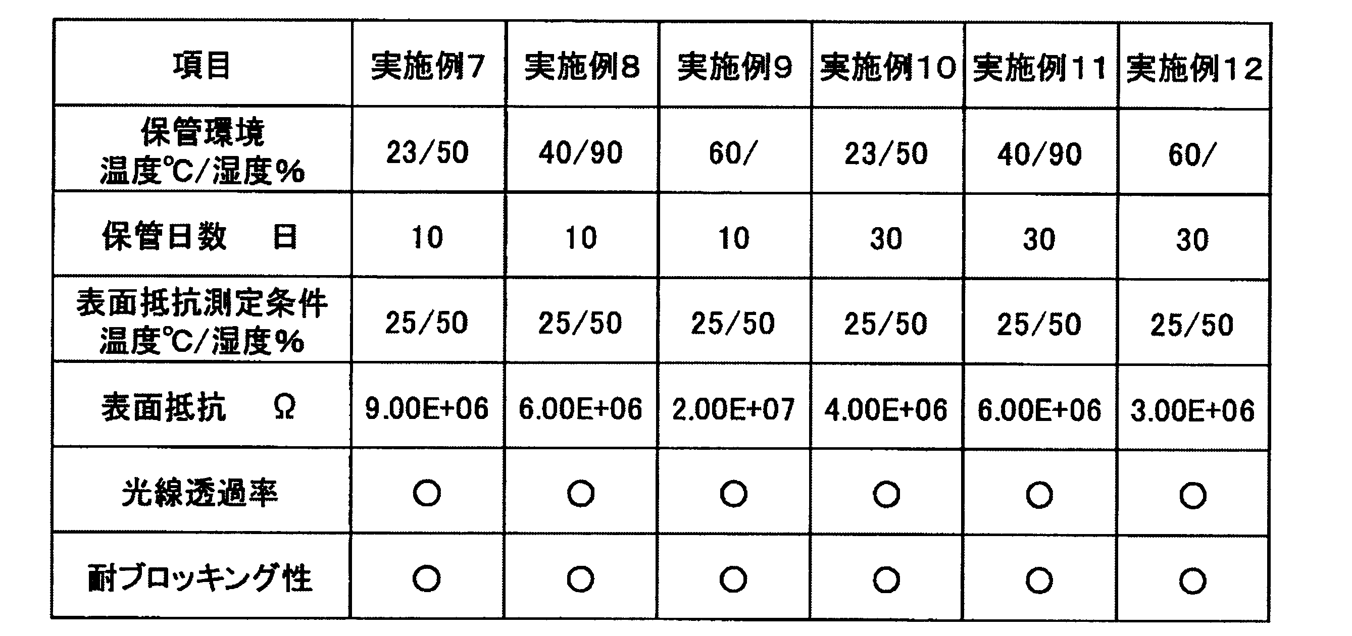
比較例1~4
カバーテープとして、住友ベークライト社製、導電タイプカバーテープのCSL-Z7302の基材層表面をアセトンで洗浄したものを用いた。このカバーテープの基材層表面に導電性界面活性剤であるポリマー界面活性剤(アクリット1SX-1090、大成ファインケミカル株式会社製)を、厚さ150nmとなる様に塗布して導電性界面活性剤を備えた比較のカバーテープを製造した。
この比較のカバーテープを、表3に示す様な保管環境及び保管日数で保管せしめ、表面抵抗、光線透過率、及びブロッキングを評価した。
得られた比較の電子部品包装用カバーテープの評価結果を表3に示す。
カバーテープとして、住友ベークライト社製、導電タイプカバーテープのCSL-Z7302の基材層表面をアセトンで洗浄したものを用いた。このカバーテープの基材層表面に導電性界面活性剤であるポリマー界面活性剤(アクリット1SX-1090、大成ファインケミカル株式会社製)を、厚さ150nmとなる様に塗布して導電性界面活性剤を備えた比較のカバーテープを製造した。
この比較のカバーテープを、表3に示す様な保管環境及び保管日数で保管せしめ、表面抵抗、光線透過率、及びブロッキングを評価した。
得られた比較の電子部品包装用カバーテープの評価結果を表3に示す。
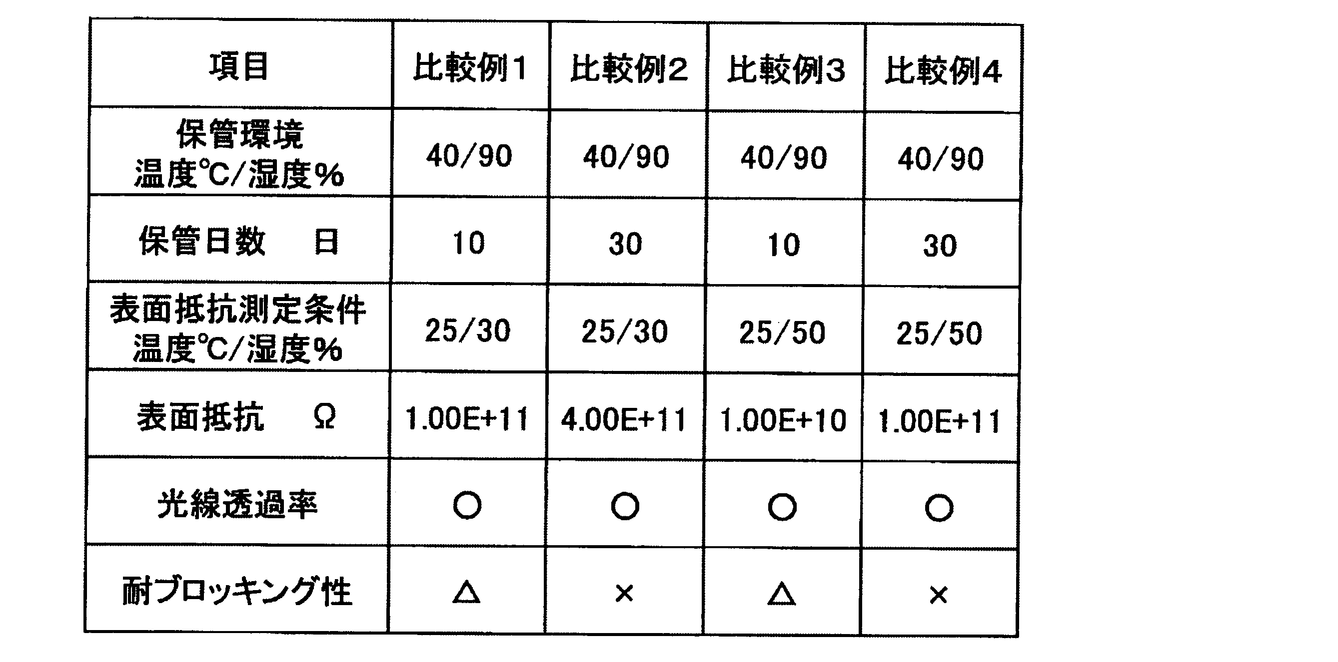
実施例13~15及び比較例5
≪供試材の作製≫
基材層として、厚さが16μmの二軸延伸ポリエステルフィルム(東洋紡績株式会社製:E5102)を準備した。
そして、基材層の一方の面にシーラント層を製膜するとともに、他方の面に以下の手順で導電性ポリマー層を製膜した。
PEDOT/PSS分散液(綜研化学社製:WED-SM)に希釈剤であるイソプロピルアルコール(IPA)と水とを加え、さらに、中和剤であるトリエチルアミン(和光純薬社製:TEA)をゆっくり加えながら30秒撹拌した。そして、バインダー樹脂として正の化合物・負の化合物(互応化学社製:プラスコートZ565、Z760、日清紡ケミカル社製:カルボジイミドV-02-L2)を加えて30秒撹拌した。この溶液をバーコーター又はグラビアコーターを用いてwet膜厚が4μmとなるように基材層の他方の面に塗布し、100℃で乾燥させることにより導電性ポリマー層を製膜した。なお、各試薬の配合重量は表4に示すとおりである。
以上の方法により、カバーテープ(供試材No.1~4)を作製した。
≪供試材の作製≫
基材層として、厚さが16μmの二軸延伸ポリエステルフィルム(東洋紡績株式会社製:E5102)を準備した。
そして、基材層の一方の面にシーラント層を製膜するとともに、他方の面に以下の手順で導電性ポリマー層を製膜した。
PEDOT/PSS分散液(綜研化学社製:WED-SM)に希釈剤であるイソプロピルアルコール(IPA)と水とを加え、さらに、中和剤であるトリエチルアミン(和光純薬社製:TEA)をゆっくり加えながら30秒撹拌した。そして、バインダー樹脂として正の化合物・負の化合物(互応化学社製:プラスコートZ565、Z760、日清紡ケミカル社製:カルボジイミドV-02-L2)を加えて30秒撹拌した。この溶液をバーコーター又はグラビアコーターを用いてwet膜厚が4μmとなるように基材層の他方の面に塗布し、100℃で乾燥させることにより導電性ポリマー層を製膜した。なお、各試薬の配合重量は表4に示すとおりである。
以上の方法により、カバーテープ(供試材No.1~4)を作製した。

≪各種測定条件≫
<摩擦帯電圧>
供試材1~4の導電性ポリマー層の表面における摩擦帯電圧は、以下の方法によって測定した(図3参照)。
(1)車輪付台座30(1.0×10¹¹Ω未満)の上に、板状のゴム体40(1.0×10¹³Ω以上)を設置し、その上に2つの四角柱状の絶縁体50(1.0×10¹³Ω以上、厚み:10mm以上)を所定の間隔を設けて設置した。そして、この2つの絶縁体50に対して、摩擦の対象として想定するキャリアテープ70を、両面テープを用いて固定した。キャリアテープ70は、8mm幅にカットしたポリスチレン系シート(電気化学社製:クリアレンCST2401)を用いた。
なお、車輪付台座30は、常に接地(アース)の状態となっていた。
(2)キャリアテープ70を、イオナイザー(春日電機社製:BLH-H)を用いて除電した。
(3)車輪付台座30を動かし、表面電位計(TREK社製:MODEL370)の測定プローブ60の下にキャリアテープ70を移動させ、除電されていることを確認した。
なお、キャリアテープ70と測定プローブ60との間隔は、1~2mmであった。
(4)導電性ポリマー層が表層となるようにカバーテープ10(幅:8mm)を棒状の支持体80(1.0×10⁹Ω未満)に巻きつけた。この支持体80は、手で支える際の帯電の影響を少なくするために、カーボン練り込みフィルムや金属などの導体で構成されているのが好ましい。
そして、カバーテープ10についても、イオナイザーを用いて除電した。
(5)車輪付台座30を動かし、キャリアテープ70を測定プローブ60の下から移動させ、支持体80に巻き付けられたカバーテープ10によりキャリアテープ70表面を摩擦した。
なお、カバーテープ10による摩擦は、車輪付台座30を固定した状態で、キャリアテープ70に対して長手方向の一方向に2回摩擦(速度:約100mm/s、距離:約50mm)するというものであった。
(6)車輪付台座30を動かし、摩擦作業後から5秒以内に測定プローブ60の下にキャリアテープ70を移動させ、摩擦帯電圧を測定した。
(7)キャリアテープ70の摩擦帯電圧を測定した結果から、カバーテープ10の導電性ポリマー層の表面における摩擦帯電圧を算出した。
なお、摩擦作業前において、キャリアテープ70と、カバーテープ10の導電性ポリマー層の表面とは、除電することにより、両者の帯電圧が0Vとなっている。よって、キャリアテープ70の摩擦帯電圧が100Vとの測定結果であった場合、カバーテープ10の導電性ポリマー層の表面における摩擦帯電圧は、-100V(=0V-100V)と算出することができる。
<摩擦帯電圧>
供試材1~4の導電性ポリマー層の表面における摩擦帯電圧は、以下の方法によって測定した(図3参照)。
(1)車輪付台座30(1.0×10¹¹Ω未満)の上に、板状のゴム体40(1.0×10¹³Ω以上)を設置し、その上に2つの四角柱状の絶縁体50(1.0×10¹³Ω以上、厚み:10mm以上)を所定の間隔を設けて設置した。そして、この2つの絶縁体50に対して、摩擦の対象として想定するキャリアテープ70を、両面テープを用いて固定した。キャリアテープ70は、8mm幅にカットしたポリスチレン系シート(電気化学社製:クリアレンCST2401)を用いた。
なお、車輪付台座30は、常に接地(アース)の状態となっていた。
(2)キャリアテープ70を、イオナイザー(春日電機社製:BLH-H)を用いて除電した。
(3)車輪付台座30を動かし、表面電位計(TREK社製:MODEL370)の測定プローブ60の下にキャリアテープ70を移動させ、除電されていることを確認した。
なお、キャリアテープ70と測定プローブ60との間隔は、1~2mmであった。
(4)導電性ポリマー層が表層となるようにカバーテープ10(幅:8mm)を棒状の支持体80(1.0×10⁹Ω未満)に巻きつけた。この支持体80は、手で支える際の帯電の影響を少なくするために、カーボン練り込みフィルムや金属などの導体で構成されているのが好ましい。
そして、カバーテープ10についても、イオナイザーを用いて除電した。
(5)車輪付台座30を動かし、キャリアテープ70を測定プローブ60の下から移動させ、支持体80に巻き付けられたカバーテープ10によりキャリアテープ70表面を摩擦した。
なお、カバーテープ10による摩擦は、車輪付台座30を固定した状態で、キャリアテープ70に対して長手方向の一方向に2回摩擦(速度:約100mm/s、距離:約50mm)するというものであった。
(6)車輪付台座30を動かし、摩擦作業後から5秒以内に測定プローブ60の下にキャリアテープ70を移動させ、摩擦帯電圧を測定した。
(7)キャリアテープ70の摩擦帯電圧を測定した結果から、カバーテープ10の導電性ポリマー層の表面における摩擦帯電圧を算出した。
なお、摩擦作業前において、キャリアテープ70と、カバーテープ10の導電性ポリマー層の表面とは、除電することにより、両者の帯電圧が0Vとなっている。よって、キャリアテープ70の摩擦帯電圧が100Vとの測定結果であった場合、カバーテープ10の導電性ポリマー層の表面における摩擦帯電圧は、-100V(=0V-100V)と算出することができる。
本実施例13~15では、カバーテープ10の静電気の放電性が優れていたことから、カバーテープ10の導電性ポリマー層の表面における摩擦帯電圧を直接測定すると、測定値に大きな誤差(揺らぎ)が生じてしまう。したがって、キャリアテープ70を測定することによって、カバーテープ10の導電性ポリマー層の表面における摩擦帯電圧の正確な値を算出することとした。
なお、参考のために、シーラント層表面における摩擦帯電圧も測定した。測定方法については、前記(4)において、導電性ポリマー層ではなく、シーラント層が表層となるようにカバーテープ10を棒状の支持体80に巻き付けた点以外、前記(1)~(7)と同様の方法により行った。
なお、参考のために、シーラント層表面における摩擦帯電圧も測定した。測定方法については、前記(4)において、導電性ポリマー層ではなく、シーラント層が表層となるようにカバーテープ10を棒状の支持体80に巻き付けた点以外、前記(1)~(7)と同様の方法により行った。
<表面抵抗値>
供試材1~4の基材層(基材層+導電性ポリマー層、シーラント層)の表面抵抗値については、IEC61340 5-1に準じて25℃、30%RHの条件下、及び25℃、50%RHの条件下で、基材層の表面抵抗値をTREK社製表面抵抗率計により測定した。
供試材1~4の基材層(基材層+導電性ポリマー層、シーラント層)の表面抵抗値については、IEC61340 5-1に準じて25℃、30%RHの条件下、及び25℃、50%RHの条件下で、基材層の表面抵抗値をTREK社製表面抵抗率計により測定した。
[規則91に基づく訂正 13.03.2015]
[結果の検討]
表4に示すように、供試材1(実施例13)は、導電性ポリマー層の表面における摩擦帯電圧(絶対値)が413Vとなり、当該表面において摩擦による帯電の発生を抑制できることがわかった。また、供試材1は、基材層(基材層+導電性ポリマー層)の表面抵抗値が5.0×10⁶Ω/□となり、帯電したとしても速やかに静電気を放電できることがわかった。
また、供試材3、4(実施例14,15)についても、導電性ポリマー層の表面における摩擦帯電圧(絶対値)が所定値以下となり、当該表面において摩擦による帯電の発生を抑制できることがわかった。
一方、供試材2(比較例5)は、導電性ポリマー層に正の化合物が含まれていなかったことから、導電性ポリマー層の表面における摩擦帯電圧(絶対値)が3000Vとなり、当該表面において摩擦による帯電の発生を十分には抑制できないことがわかった。
[結果の検討]
表4に示すように、供試材1(実施例13)は、導電性ポリマー層の表面における摩擦帯電圧(絶対値)が413Vとなり、当該表面において摩擦による帯電の発生を抑制できることがわかった。また、供試材1は、基材層(基材層+導電性ポリマー層)の表面抵抗値が5.0×10⁶Ω/□となり、帯電したとしても速やかに静電気を放電できることがわかった。
また、供試材3、4(実施例14,15)についても、導電性ポリマー層の表面における摩擦帯電圧(絶対値)が所定値以下となり、当該表面において摩擦による帯電の発生を抑制できることがわかった。
一方、供試材2(比較例5)は、導電性ポリマー層に正の化合物が含まれていなかったことから、導電性ポリマー層の表面における摩擦帯電圧(絶対値)が3000Vとなり、当該表面において摩擦による帯電の発生を十分には抑制できないことがわかった。
1 基材層
2 シーラント層
3 導電性ポリマー層
10 電子部品包装用カバーテープ(カバーテープ)
10a カバーテープの表面(導電性ポリマー層の表面)
20 キャリアテープ
20a キャリアテープの底面
100 包装体
2 シーラント層
3 導電性ポリマー層
10 電子部品包装用カバーテープ(カバーテープ)
10a カバーテープの表面(導電性ポリマー層の表面)
20 キャリアテープ
20a キャリアテープの底面
100 包装体
Claims (16)
- [規則91に基づく訂正 13.03.2015]
基材層と、
前記基材層の一方の面側に設けられるシーラント層と、
前記基材層の他方の面側に設けられる導電性ポリマー層と、
を備えることを特徴とする電子部品包装用カバーテープ。 - 前記基材層は、85%以上の光線透過率を有し、
前記導電性ポリマー層を設けた前記基材層は、温度25℃の温度環境下において、相対湿度12%以上50%以下に渡って、1×10⁹Ω/□以下の表面抵抗値を有することを特徴とする請求項1に記載の電子部品包装用カバーテープ。 - 前記基材層はポリエステル、ポリプロピレン、またはナイロンから選ばれる少なくとも1種以上を含有する二軸延伸フィルムであること
を特徴とする請求項1または2に記載の電子部品包装用カバーテープ。 - 前記導電性ポリマー層がポリ(3,4-エチレンジオキシチオフェン)を含有することを特徴とする請求項1または2に記載の電子部品包装用カバーテープ。
- 前記導電性ポリマー層がポリスチレンスルホン酸を更に含有することを特徴とする請求項4に記載の電子部品包装用カバーテープ。
- 前記シーラント層は、温度25℃の温度環境下において、相対湿度12%以上50%以下に渡って、1×10¹¹Ω/□未満の表面抵抗値を有することを特徴とする請求項1または2に記載の電子部品包装用カバーテープ。
- 前記導電性ポリマー層がシリカ粒子を含有することを特徴とする請求項1または2に記載の電子部品包装用カバーテープ。
- 前記導電性ポリマー層の表面における摩擦帯電圧が-2200~2200Vであることを特徴とする請求項1に記載の電子部品包装用カバーテープ。
- 前記導電性ポリマー層の表面における摩擦帯電圧が-800~800Vであることを特徴とする請求項1又は8に記載の電子部品包装用カバーテープ。
- 前記導電性ポリマー層は、前記導電性ポリマー層の摩擦の対象となる材料よりも帯電列において正側に位置する正の化合物と、前記摩擦の対象となる材料よりも帯電列において負側に位置する負の化合物と、を含むことを特徴とする請求項1又は8に記載の電子部品包装用カバーテープ。
- 前記導電性ポリマー層は、エステル化合物を含むことを特徴とする請求項1から8に記載の電子部品包装用カバーテープ。
- 前記導電性ポリマー層は、アジリジニル化合物及びその開環化合物の少なくとも一方を含むことを特徴とする請求項1から8に記載の電子部品包装用カバーテープ。
- 前記導電性ポリマー層を設けた前記基材層は、温度25℃、湿度12~65%RHという環境下における表面抵抗値が1×10¹¹Ω/□以下であることを特徴とする請求項1又は8に記載の電子部品包装用カバーテープ。
- 前記基材層は、全光線透過率が85%以上であることを特徴とする請求項1又は8に記載の電子部品包装用カバーテープ。
- 前記導電性ポリマー層は、
アジリジニル化合物及びその開環化合物の少なくとも一方と、
ポリ(3,4-エチレンジオキシチオフェン)とを
含有することを特徴とする請求項1に記載の電子部品包装用カバーテープ。 - 前記導電性ポリマー層は、
ポリスチレンスルホン酸とを更に
含有することを特徴とする請求項15に記載の電子部品包装用カバーテープ。
Priority Applications (2)
| Application Number | Priority Date | Filing Date | Title |
|---|---|---|---|
| CN201580005861.1A CN105934396B (zh) | 2014-01-29 | 2015-01-23 | 电子部件包装用盖带 |
| KR1020167020387A KR20160114602A (ko) | 2014-01-29 | 2015-01-23 | 전자 부품 포장용 커버 테이프 |
Applications Claiming Priority (4)
| Application Number | Priority Date | Filing Date | Title |
|---|---|---|---|
| JP2014013989A JP2015140200A (ja) | 2014-01-29 | 2014-01-29 | 電子部品包装用カバーテープ |
| JP2014-013989 | 2014-01-29 | ||
| JP2014198471A JP2016068987A (ja) | 2014-09-29 | 2014-09-29 | 電子部品包装用カバーテープ |
| JP2014-198471 | 2014-09-29 |
Publications (1)
| Publication Number | Publication Date |
|---|---|
| WO2015115338A1 true WO2015115338A1 (ja) | 2015-08-06 |
Family
ID=53756912
Family Applications (1)
| Application Number | Title | Priority Date | Filing Date |
|---|---|---|---|
| PCT/JP2015/051933 Ceased WO2015115338A1 (ja) | 2014-01-29 | 2015-01-23 | 電子部品包装用カバーテープ |
Country Status (4)
| Country | Link |
|---|---|
| KR (1) | KR20160114602A (ja) |
| CN (1) | CN105934396B (ja) |
| TW (1) | TWI620695B (ja) |
| WO (1) | WO2015115338A1 (ja) |
Cited By (3)
| Publication number | Priority date | Publication date | Assignee | Title |
|---|---|---|---|---|
| JP2017109753A (ja) * | 2015-12-15 | 2017-06-22 | 住友ベークライト株式会社 | 電子部品包装用カバーテープ |
| JP2017128354A (ja) * | 2016-01-19 | 2017-07-27 | 住友ベークライト株式会社 | 電子部品包装用カバーテープ |
| WO2021070935A1 (ja) * | 2019-10-11 | 2021-04-15 | 大日本印刷株式会社 | 電子部品包装用カバーテープおよび包装体 |
Families Citing this family (6)
| Publication number | Priority date | Publication date | Assignee | Title |
|---|---|---|---|---|
| CN110683208A (zh) * | 2018-07-06 | 2020-01-14 | 3M创新有限公司 | 多层盖带构造 |
| DE102018217907B3 (de) | 2018-10-19 | 2019-12-19 | SpinDiag GmbH | Probenbehälter |
| KR102232958B1 (ko) | 2020-12-08 | 2021-03-26 | 김동준 | 방수목적의 전자부품 이송 및 표면 실장을 위한 커버테이프 및 그 제조장치 |
| CN114133709A (zh) * | 2021-11-30 | 2022-03-04 | 浙江洁美电子科技股份有限公司 | 一种导电性片材及微型封装件用载带 |
| KR102542727B1 (ko) | 2022-10-25 | 2023-06-14 | (주)켐텍솔루션 | 전자 부품 포장용 커버 테이프의 접착층 형성을 위한 액상 수지 조성물 및 이를 이용하여 제조된 커버 테이프 |
| JP7409543B1 (ja) * | 2023-03-24 | 2024-01-09 | 住友ベークライト株式会社 | 電子部品包装用カバーテープおよび電子部品包装体 |
Citations (6)
| Publication number | Priority date | Publication date | Assignee | Title |
|---|---|---|---|---|
| JP2000142788A (ja) * | 1998-11-09 | 2000-05-23 | Shin Etsu Polymer Co Ltd | カバーテープとその製造方法 |
| JP2001301819A (ja) * | 2000-04-27 | 2001-10-31 | Achilles Corp | 導電性カバーテープ |
| JP2002193377A (ja) * | 2000-12-27 | 2002-07-10 | Sumitomo Bakelite Co Ltd | 電子部品包装用カバーテープ |
| JP2003128132A (ja) * | 2001-10-16 | 2003-05-08 | Denki Kagaku Kogyo Kk | カバーテープ |
| JP2004058648A (ja) * | 2001-12-06 | 2004-02-26 | Toray Ind Inc | 積層フィルム、および、積層フィルムの製造方法 |
| JP2005081766A (ja) * | 2003-09-10 | 2005-03-31 | Mitsubishi Rayon Co Ltd | 導電性包装材料、その製造方法および電子部品用容器 |
Family Cites Families (15)
| Publication number | Priority date | Publication date | Assignee | Title |
|---|---|---|---|---|
| US4800115A (en) | 1986-10-14 | 1989-01-24 | W. R. Grace & Co. | Agent for imparting antistatic characteristics to a thermoplastic polymer and a thermoplastic polymer composition containing the agent |
| JP2001106256A (ja) | 1999-10-07 | 2001-04-17 | Sumitomo Bakelite Co Ltd | 電子部品包装用カバーテープ |
| JP3514699B2 (ja) | 2000-05-01 | 2004-03-31 | 電気化学工業株式会社 | カバーテープ |
| KR100856371B1 (ko) * | 2001-05-28 | 2008-09-04 | 덴끼 가가꾸 고교 가부시키가이샤 | 전자부품 용기 |
| EP1270210B1 (en) * | 2001-06-26 | 2006-08-16 | Sumitomo Bakelite Company Limited | Cover tape for packaging electronic components |
| TWI269709B (en) * | 2001-12-06 | 2007-01-01 | Toray Industries | Laminated film and process for producing laminated film |
| JP2004001876A (ja) | 2002-03-01 | 2004-01-08 | Dainippon Ink & Chem Inc | 密着防止層を有するキャリアテープ用カバーテープ |
| JP2004051105A (ja) | 2002-07-16 | 2004-02-19 | Dainippon Printing Co Ltd | カバーテープ |
| JP2004262548A (ja) | 2003-02-12 | 2004-09-24 | Shin Etsu Polymer Co Ltd | カバーテープ及び包装体 |
| JP2012030897A (ja) | 2005-04-07 | 2012-02-16 | Sumitomo Bakelite Co Ltd | 電子部品包装用カバーテープ |
| JP4878869B2 (ja) * | 2005-04-08 | 2012-02-15 | 日東電工株式会社 | 発泡部材、発泡部材積層体及び発泡部材が用いられた電気・電子機器類 |
| JP5104109B2 (ja) | 2007-08-02 | 2012-12-19 | 東ソー株式会社 | 接着剤及びそれを用いた易剥離性フィルム |
| JP5509462B2 (ja) | 2009-02-27 | 2014-06-04 | ナガセケムテックス株式会社 | 導電性コーティング用組成物 |
| JP2012214252A (ja) | 2010-09-30 | 2012-11-08 | Sumitomo Bakelite Co Ltd | 電子部品包装用カバーテープ |
| JP5602067B2 (ja) | 2011-03-09 | 2014-10-08 | 三井・デュポンポリケミカル株式会社 | シーラント材、カバーテープ、及び電子部品搬送用包装体 |
-
2015
- 2015-01-23 CN CN201580005861.1A patent/CN105934396B/zh not_active Expired - Fee Related
- 2015-01-23 KR KR1020167020387A patent/KR20160114602A/ko not_active Ceased
- 2015-01-23 WO PCT/JP2015/051933 patent/WO2015115338A1/ja not_active Ceased
- 2015-01-26 TW TW104102435A patent/TWI620695B/zh not_active IP Right Cessation
Patent Citations (6)
| Publication number | Priority date | Publication date | Assignee | Title |
|---|---|---|---|---|
| JP2000142788A (ja) * | 1998-11-09 | 2000-05-23 | Shin Etsu Polymer Co Ltd | カバーテープとその製造方法 |
| JP2001301819A (ja) * | 2000-04-27 | 2001-10-31 | Achilles Corp | 導電性カバーテープ |
| JP2002193377A (ja) * | 2000-12-27 | 2002-07-10 | Sumitomo Bakelite Co Ltd | 電子部品包装用カバーテープ |
| JP2003128132A (ja) * | 2001-10-16 | 2003-05-08 | Denki Kagaku Kogyo Kk | カバーテープ |
| JP2004058648A (ja) * | 2001-12-06 | 2004-02-26 | Toray Ind Inc | 積層フィルム、および、積層フィルムの製造方法 |
| JP2005081766A (ja) * | 2003-09-10 | 2005-03-31 | Mitsubishi Rayon Co Ltd | 導電性包装材料、その製造方法および電子部品用容器 |
Cited By (4)
| Publication number | Priority date | Publication date | Assignee | Title |
|---|---|---|---|---|
| JP2017109753A (ja) * | 2015-12-15 | 2017-06-22 | 住友ベークライト株式会社 | 電子部品包装用カバーテープ |
| JP2017128354A (ja) * | 2016-01-19 | 2017-07-27 | 住友ベークライト株式会社 | 電子部品包装用カバーテープ |
| WO2021070935A1 (ja) * | 2019-10-11 | 2021-04-15 | 大日本印刷株式会社 | 電子部品包装用カバーテープおよび包装体 |
| JP2021062881A (ja) * | 2019-10-11 | 2021-04-22 | 大日本印刷株式会社 | 電子部品包装用カバーテープおよび包装体 |
Also Published As
| Publication number | Publication date |
|---|---|
| KR20160114602A (ko) | 2016-10-05 |
| CN105934396A (zh) | 2016-09-07 |
| TW201540617A (zh) | 2015-11-01 |
| CN105934396B (zh) | 2018-12-18 |
| TWI620695B (zh) | 2018-04-11 |
Similar Documents
| Publication | Publication Date | Title |
|---|---|---|
| TWI620695B (zh) | 電子零件包裝用包裝體 | |
| CN103153810B (zh) | 电子部件包装用盖带 | |
| JP3966171B2 (ja) | 積層フィルム、および、積層フィルムの製造方法 | |
| TWI406889B (zh) | 抗靜電聚酯膜的製造方法,因此而製得的抗靜電聚酯膜及其用途 | |
| EP1452304B1 (en) | Layered film and process for producing layered film | |
| EP2628690B1 (en) | Cover film | |
| JP6936009B2 (ja) | 偏光板 | |
| JP7087232B2 (ja) | 帯電防止用塗布液組成物及びこれを利用した帯電防止ポリエステルフィルム | |
| JP2015140200A (ja) | 電子部品包装用カバーテープ | |
| JP7590263B2 (ja) | 表面保護フィルムおよび光学部品 | |
| CN202322704U (zh) | 一种抗静电保护膜 | |
| KR20160085058A (ko) | 포장재용 적층 필름 및 이를 이용한 포장 봉투 | |
| JP2019031658A (ja) | 導電性高分子分散液、導電性フィルム及びその製造方法、並びに帯電防止性容器及びその製造方法 | |
| JP2016064625A (ja) | 積層フィルム | |
| JP2016068987A (ja) | 電子部品包装用カバーテープ | |
| JP6011750B1 (ja) | 電子部品包装用カバーテープおよび電子部品用包装体 | |
| KR101660532B1 (ko) | 기능성 광학필름 | |
| KR100965106B1 (ko) | 도전성 코팅제, 이를 이용한 무연신 도전시트 및 이로부터성형된 포장재 | |
| TWI892499B (zh) | 覆蓋帶、電子零件包裝體及覆蓋帶之製造方法 | |
| JP2025055876A (ja) | カバーテープおよび電子部品包装体 | |
| KR20120007815A (ko) | 대전방지 이형필름 및 그것의 제조방법 | |
| TWI478952B (zh) | 導電聚酯膜 | |
| JP2025133188A (ja) | カバーテープ巻取品および電子部品包装体 | |
| JP2017013803A (ja) | 電子部品包装用カバーテープ | |
| WO2024195802A1 (ja) | 電子部品包装用カバーテープおよび包装体 |
Legal Events
| Date | Code | Title | Description |
|---|---|---|---|
| 121 | Ep: the epo has been informed by wipo that ep was designated in this application |
Ref document number: 15743580 Country of ref document: EP Kind code of ref document: A1 |
|
| ENP | Entry into the national phase |
Ref document number: 20167020387 Country of ref document: KR Kind code of ref document: A |
|
| NENP | Non-entry into the national phase |
Ref country code: DE |
|
| 122 | Ep: pct application non-entry in european phase |
Ref document number: 15743580 Country of ref document: EP Kind code of ref document: A1 |