WO2015111408A1 - 電流検出システム - Google Patents
電流検出システム Download PDFInfo
- Publication number
- WO2015111408A1 WO2015111408A1 PCT/JP2015/000283 JP2015000283W WO2015111408A1 WO 2015111408 A1 WO2015111408 A1 WO 2015111408A1 JP 2015000283 W JP2015000283 W JP 2015000283W WO 2015111408 A1 WO2015111408 A1 WO 2015111408A1
- Authority
- WO
- WIPO (PCT)
- Prior art keywords
- magnetic plate
- bus bar
- magnetic
- conversion element
- detection system
- Prior art date
- Legal status (The legal status is an assumption and is not a legal conclusion. Google has not performed a legal analysis and makes no representation as to the accuracy of the status listed.)
- Ceased
Links
Images





Classifications
-
- G—PHYSICS
- G01—MEASURING; TESTING
- G01R—MEASURING ELECTRIC VARIABLES; MEASURING MAGNETIC VARIABLES
- G01R15/00—Details of measuring arrangements of the types provided for in groups G01R17/00 - G01R29/00, G01R33/00 - G01R33/26 or G01R35/00
- G01R15/14—Adaptations providing voltage or current isolation, e.g. for high-voltage or high-current networks
- G01R15/20—Adaptations providing voltage or current isolation, e.g. for high-voltage or high-current networks using galvano-magnetic devices, e.g. Hall-effect devices, i.e. measuring a magnetic field via the interaction between a current and a magnetic field, e.g. magneto resistive or Hall effect devices
- G01R15/205—Adaptations providing voltage or current isolation, e.g. for high-voltage or high-current networks using galvano-magnetic devices, e.g. Hall-effect devices, i.e. measuring a magnetic field via the interaction between a current and a magnetic field, e.g. magneto resistive or Hall effect devices using magneto-resistance devices, e.g. field plates
-
- G—PHYSICS
- G01—MEASURING; TESTING
- G01R—MEASURING ELECTRIC VARIABLES; MEASURING MAGNETIC VARIABLES
- G01R33/00—Arrangements or instruments for measuring magnetic variables
- G01R33/02—Measuring direction or magnitude of magnetic fields or magnetic flux
- G01R33/06—Measuring direction or magnitude of magnetic fields or magnetic flux using galvano-magnetic devices
- G01R33/09—Magnetoresistive devices
-
- G—PHYSICS
- G01—MEASURING; TESTING
- G01R—MEASURING ELECTRIC VARIABLES; MEASURING MAGNETIC VARIABLES
- G01R15/00—Details of measuring arrangements of the types provided for in groups G01R17/00 - G01R29/00, G01R33/00 - G01R33/26 or G01R35/00
- G01R15/14—Adaptations providing voltage or current isolation, e.g. for high-voltage or high-current networks
- G01R15/20—Adaptations providing voltage or current isolation, e.g. for high-voltage or high-current networks using galvano-magnetic devices, e.g. Hall-effect devices, i.e. measuring a magnetic field via the interaction between a current and a magnetic field, e.g. magneto resistive or Hall effect devices
- G01R15/207—Constructional details independent of the type of device used
-
- G—PHYSICS
- G01—MEASURING; TESTING
- G01R—MEASURING ELECTRIC VARIABLES; MEASURING MAGNETIC VARIABLES
- G01R33/00—Arrangements or instruments for measuring magnetic variables
- G01R33/02—Measuring direction or magnitude of magnetic fields or magnetic flux
- G01R33/06—Measuring direction or magnitude of magnetic fields or magnetic flux using galvano-magnetic devices
- G01R33/09—Magnetoresistive devices
- G01R33/091—Constructional adaptation of the sensor to specific applications
Definitions
- the present disclosure includes Japanese application number 2014-10659 filed on January 23, 2014, Japanese application number 2014-70021 filed on March 28, 2014, and filed on January 16, 2015. Which is based on Japanese Patent Application No. 2015-7086, which is incorporated herein by reference.
- the present disclosure relates to a current detection system including a magnetic plate, a bus bar, and a magnetoelectric conversion element.
- a magnetic shield that forms a magnetically shielded region and a magnetic detection element provided in the magnetically shielded region, and a current flowing through the conductor
- a current detection device for detecting a value by a magnetic detection element has been proposed.
- the magnetic shield is a pair of magnetic plates having the same dimensions, and the conductor is a wide plate-like bus bar.
- the pair of magnetic plates are arranged opposite to each other in the y direction so as to sandwich both side edges of the bus bar in the width direction from the outside.
- the magnetic detection elements are installed facing the center in the width direction of the bus bar, and the bus bars and the magnetic detection elements are arranged in the z direction orthogonal to the y direction.
- the magnetic detection element detects a magnetic flux along a direction orthogonal to the z direction (for example, the y direction).
- a pair of magnetic plates are arranged in the y direction.
- the magnetic detection element detects a magnetic flux along a direction orthogonal to the z direction (for example, the y direction). Therefore, when an external magnetic flux along the y direction is applied, the magnetic detection element detects not only the magnetic flux corresponding to the current flowing through the bus bar but also the external magnetic flux. As a result, the detection accuracy of the current flowing through the bus bar may be reduced.
- an object of the present disclosure is to provide a current detection system in which a decrease in current detection accuracy is suppressed.
- the current detection system includes a first magnetic plate and a second magnetic plate arranged in parallel at a predetermined interval in the height direction, and a current flows in a depth direction orthogonal to the height direction.
- the storage space is divided into a transmission space through which the external magnetic flux passes and a non-transmission space through which the external magnetic flux does not pass.
- the bus bar is provided in the storage space.
- the magnetoelectric conversion element is provided in the non-transmissive space.
- the bus bar and the magnetoelectric transducer are arranged side by side in the height direction.
- the first magnetic plate and the second magnetic plate are arranged in the height direction.
- the trajectory of the transverse magnetic flux orthogonal to the height direction is bent by the first magnetic plate and the second magnetic plate, and a non-transmission space through which external magnetic flux is not transmitted is mainly formed.
- the trajectory is not so bent by the magnetic plate, and the component in the height direction is kept constant.
- the magnetoelectric conversion element does not detect the external magnetic flux along the height direction, so that a decrease in detection accuracy of the current flowing through the bus bar is suppressed.
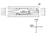
- FIG. 1 is a cross-sectional view illustrating a schematic configuration of a current detection system according to the first embodiment.
- FIG. 2 is a cross-sectional view for explaining the transmission space and the non-transmission space
- FIG. 3 is a cross-sectional view showing a modification of the current detection system
- FIG. 4 is a cross-sectional view showing a modification of the current detection system
- FIG. 7 is a perspective view showing a modification of the magnetic plate
- FIG. 8 is a graph showing the relationship between the shielding level and the aspect ratio when the separation distance is changed
- FIG. 9 is a graph showing the relationship between the shielding level and the aspect ratio when the magnetic permeability is changed.
- x direction three directions that are orthogonal to each other are indicated as an x direction, a y direction, and a z direction.
- the plane defined by the x direction and the y direction is the xy plane
- the plane defined by the y direction and the z direction is the yz plane
- the plane defined by the z direction and the x direction is z ⁇ . Shown as x-plane.
- the x direction corresponds to the horizontal direction
- the y direction corresponds to the depth direction
- the z direction corresponds to the height direction.
- the current detection system 100 includes a first magnetic plate 10, a second magnetic plate 20, a bus bar 30, and a semiconductor substrate 40.
- the magnetic plates 10 and 20 are arranged in parallel at a predetermined interval in the z direction, and constitute a storage space SS therebetween.
- the bus bar 30 and the semiconductor substrate 40 are stored in the storage space SS.
- the bus bar 30 passes a current in the y direction, thereby forming a magnetic flux to be measured.
- the semiconductor substrate 40 is formed with a magnetoelectric conversion element 41 for converting magnetic flux into an electric signal.
- the magnetoelectric conversion element 41 converts the magnetic flux to be measured into an electric signal.
- Each of the magnetic plates 10 and 20 is made of a material having a higher magnetic permeability than air, and suppresses intrusion of external magnetic flux into the storage space SS.
- Each of the magnetic plates 10 and 20 has a plate shape in which the main surface is along the xy plane, and a cross-sectional shape in the zx plane is a rectangle. As shown in FIGS. 1 and 2, the short side direction of the rectangle is along the z direction, and the long side direction is along the x direction.
- the separation distance in the z direction between the main surfaces (inner surfaces) 10a and 20a of the magnetic plates 10 and 20 is constant, which is a parallel relationship. Therefore, the cross-sectional shape in the zx plane in the storage space SS is also rectangular.
- the current to be measured flows through the bus bar 30.
- the bus bar 30 has a bar shape extending in the y direction, and has a rectangular cross-sectional shape in the zx plane as shown in FIGS.
- the short direction is along the z direction
- the long direction is along the x direction.
- the measured current flows in the y direction. Therefore, a measured magnetic flux penetrating the yz plane is formed by the flow of the measured current.
- the x component of the magnetic flux to be measured is converted into an electric signal by the magnetoelectric conversion element 41.
- a magnetoelectric conversion element 41 is formed on a surface 40 a of the semiconductor substrate 40 facing the first magnetic plate 10.
- the magnetoelectric conversion element 41 has a function of converting a component in the x direction of the magnetic flux to be measured into an electric signal.
- the magnetoelectric conversion element 41 according to the present embodiment has a function of converting a magnetic flux to be measured not only in the x direction but also along the xy plane into an electric signal.
- the magnetoelectric conversion element 41 according to the present embodiment is a magnetoresistive effect element whose resistance value varies with application of magnetic flux.
- the magnetoelectric conversion element 41 includes a pinned layer whose magnetization direction is fixed, a free layer whose magnetization direction varies according to an applied magnetic field, a nonmagnetic intermediate layer provided between the pinned layer and the free layer, Have The magnetoelectric conversion element 41 has a property that its resistance value varies according to the angle formed by the magnetization directions of the pinned layer and the free layer.
- the magnetization direction of the pinned layer is along one direction along the xy plane, and the magnetization direction of the free layer has a property that its direction varies in the xy plane.
- the magnetoelectric conversion element 41 When the intermediate layer has conductivity, the magnetoelectric conversion element 41 is a giant magnetoresistance effect element (GMR), and when the intermediate layer has insulation, the magnetoelectric conversion element 41 is a tunnel magnetoresistance effect element (TMR). Of course, instead of these, an anisotropic magnetoresistive element (AMR) can be adopted.
- the facing surface 40a described above corresponds to the formation surface.
- the magnetic plates 10 and 20 are arranged in parallel at a predetermined interval in the z direction, and the bus bar 30 and the semiconductor substrate 40 are stored in the storage space SS formed therebetween.
- the storage space SS is mainly divided into a transmission space PS through which external magnetic flux is transmitted and a non-transmission space NPS (space surrounded by a broken line) through which external magnetic flux is not transmitted.
- the size of the non-transmission space NPS through which the external magnetic flux is not transmitted and the shielding level thereof are determined by the intention of the designer to how much the external magnetic flux is shielded.
- the size of the non-transmission space NPS is proportional to the formation material, the lateral width of each of the magnetic plates 10 and 20, and the separation distance (gap) between them in the z direction. Therefore, the designer can design a non-transparent space NPS having a desired shielding level and size by appropriately adjusting these parameters.
- the shielding level of the external magnetic flux in the non-transmissive space NPS is set to be 99% or less.
- permalloy is set as a forming material, 20 mm as a lateral width, and 5 mm as a gap.
- each of the magnetic plates 10 and 20 has a flat surface along the xy plane, so that not only the external magnetic flux along the x direction but also the external magnetic flux along the xy plane. It also functions as a shield.
- the magnetoelectric conversion element 41 is provided in the non-transparent space NPS, and is arranged side by side with the bus bar 30 in the z direction.
- the center CP of the storage space SS is located at the center of the non-transparent space NPS, and the center of the magnetoelectric conversion element 41 is located on a reference line BL (one-dot chain line shown in FIG. 1) passing through the center in the x direction. ing. Further, the geometric center of each of the magnetoelectric transducer 41 and the bus bar 30 and the geometric center of each of the magnetic plates 10 and 20 are penetrated by a center line CL (broken line shown in FIG. 1) along the z direction. .
- the distance between the two ends of each of the magnetic plates 10 and 20 and the geometric center of the bus bar 30 in the x direction is the same, and the two ends of each of the magnetic plates 10 and 20 and the magnetoelectric transducer 41 The distance to the geometric center is the same.
- the facing surface 40a of the semiconductor substrate 40 on which the magnetoelectric conversion element 41 is formed and the inner surface 10a of the first magnetic plate 10 face each other in the z direction, and the separation distance between the facing surface 40a and the inner surface 10a is constant, It is a parallel relationship.
- the separation distance between the facing surface 30a of the bus bar 30 and the inner surface 20a of the second magnetic plate 20 is constant and is in a parallel relationship.
- the current detection system 100 has a line-symmetric shape through the center line CL in the zx plane.
- the first magnetic plate 10 and the second magnetic plate 20 are arranged in the z direction.
- the orbit of the magnetic flux in the x direction orthogonal to the z direction is bent by the first magnetic plate 10 and the second magnetic plate 20 to form a non-transparent space NPS that does not mainly transmit external magnetic flux.
- the magnetic flux along the z direction its trajectory is not bent much by the magnetic plate, and the component in the z direction is kept constant.
- the bus bar and the magnetoelectric conversion element are arranged in the x direction in the storage space, and the magnetoelectric conversion element detects the z direction component of the measured magnetic flux.
- the magnetoelectric transducer detects the external magnetic flux along the z direction
- the current flowing through the bus bar cannot be detected with high accuracy.
- the bus bar 30 and the magnetoelectric conversion element 41 are arranged in the z direction in the storage space SS, and the magnetoelectric conversion element 41 detects a component in the x direction of the magnetic flux to be measured. Therefore, unlike the above-described comparative configuration, the magnetoelectric conversion element 41 does not detect the external magnetic flux along the z direction, so that a decrease in detection accuracy of the current flowing through the bus bar 30 is suppressed.
- the magnetoelectric conversion element 41 is a magnetoresistive effect element.
- the magnetoelectric conversion element 41 is not limited to the above example, and any element that can convert a magnetic signal into an electric signal can be used as appropriate.
- a Hall element that converts magnetic flux along the x direction into a voltage by the Hall effect can be adopted.
- the shielding level of the external magnetic flux in the non-transparent space NPS is set to be 99% or less.
- how much the external magnetic flux is shielded is a matter determined by the designer and is not limited to the above example.
- the shielding level may be 90%.
- each of the magnetic plates 10 and 20 is permalloy
- the lateral width is 20 mm
- the gap between the two is set to 5 mm.
- the forming material, the width, and the gap of each of the magnetic plates 10 and 20 can be appropriately changed according to the shielding level.
- an electromagnetic steel plate, a width of 30 mm, and a gap of 5 mm can be employed. Even with this combination, the external magnetic flux can be suppressed to 99% or less.
- the thickness (the length in the z direction) of each of the magnetic plates 10 and 20 is not defined.
- the thickness of each of the magnetic plates 10 and 20 is appropriately determined so that the magnetic flux inside each of the magnetic plates 10 and 20 is not saturated by the external magnetic flux or the magnetic flux to be measured. If each of the magnetic plates 10 and 20 is not saturated, the thickness does not depend on the formation of each of the transmission space PS and the non-transmission space NPS.
- each of the magnetic plates 10 and 20 shields not only the external magnetic flux along the x direction but also the external magnetic flux along the xy plane.
- the magnetoelectric conversion element 41 performs the function of converting only the magnetic flux along the x direction into an electric signal
- the magnetic plates 10 and 20 may only perform the function of shielding only the external magnetic flux along the x direction.
- the center of the magnetoelectric conversion element 41 is located on the reference line BL passing through the center CP of the storage space SS in the x direction.
- the center of the magnetoelectric conversion element 41 may not be located on the reference line BL.
- the geometric centers of the magnetoelectric transducer 41 and the bus bar 30 and the geometric centers of the magnetic plates 10 and 20 are penetrated by the center line CL.
- the geometric centers of the magnetoelectric conversion element 41, the bus bar 30, and the magnetic plates 10 and 20 may not be penetrated by the center line CL, and may not be aligned in the z direction.
- the distance between the two ends of each of the magnetic plates 10 and 20 and the geometric center of the bus bar 30 are equal, and the two ends of each of the magnetic plates 10 and 20 and the magnetoelectric conversion element.
- An example is shown in which the distances from 41 geometric centers are equal.
- the distance between the two ends of each of the magnetic plates 10 and 20 and the geometric center of the bus bar 30 is different, and the two ends of each of the magnetic plates 10 and 20 and the geometry of the magnetoelectric transducer 41 are different.
- the distances from the academic center may be different.
- the distance between the facing surface 40a of the semiconductor substrate 40 and the inner surface 10a of the first magnetic plate 10 is constant and parallel.
- the distance between the facing surface 40a and the inner surface 10a is indefinite and does not have to be in a parallel relationship.
- the distance between the facing surface 30a of the bus bar 30 and the inner surface 20a of the second magnetic plate 20 is constant and parallel.
- the distance between the facing surface 30a and the inner surface 20a is indefinite and does not have to be in a parallel relationship.
- the current detection system 100 has a line-symmetric shape in the zx plane via the center line CL.
- the current detection system 100 may not have a line-symmetric shape via the center line CL.
- the current detection system 100 includes a pair of magnetic plates 10 and 20, one bus bar 30 corresponding to these, and one semiconductor substrate 40.
- the numbers of the magnetic plates 10 and 20, the bus bar 30, and the semiconductor substrate 40 are not limited.
- the current detection system 100 may include two sets of magnetic plates 10 and 20, two bus bars 30 corresponding to these, and two semiconductor substrates 40.
- the current detection system 100 may include three sets of magnetic plates 10 and 20, three bus bars 30 corresponding to these, and three semiconductor substrates 40.
- the current detection system 100 may include a pair of magnetic plates 10 and 20, two bus bars 30 corresponding to these, and two semiconductor substrates 40.
- the current detection system 100 may include a pair of magnetic plates 10 and 20, three bus bars 30 corresponding to these, and three semiconductor substrates 40.
- the number of parts can be reduced and the size can be reduced.
- the shape of each of the magnetic plates 10 and 20 on the xy plane (hereinafter referred to as a planar shape) is not particularly limited.
- the planar shape of each of the magnetic plates 10 and 20 is not particularly limited as long as the non-transparent space NPS can be formed.
- a polygonal shape such as a rectangle or a circle can be adopted as the planar shape.
- FIG. 7 shows an example in which the planar shape of the magnetic plates 10 and 20 is an octagon.
- the relationship between the lateral width and the separation distance of each of the magnetic plates 10 and 20 was not particularly described.
- the inner surface 10 a partially opposed to the magnetoelectric conversion element 41 in the first magnetic plate 10 and the inner surface 20 a partially opposed to the bus bar 30 in the second magnetic plate 20 are separated in the z direction. If the distance is constant and parallel, the following relationship should be satisfied. That is, when the separation distance in the z direction between the inner surface 10a and the inner surface 20a is h, and the lateral width (longest length) of each of the first magnetic plate 10 and the second magnetic plate 20 in the x direction is w, FIG. 8 and FIG. As shown, an aspect ratio w / h between the separation distance h and the lateral width w is preferably 4 or more.
- FIG. 8 shows the relationship between the shielding level and the aspect ratio w / h when the separation distance h of the magnetic plates 10 and 20 is changed from 3.8 to 5.6 mm.
- FIG. 9 shows the relationship between the shielding level and the aspect ratio w / h when the magnetic permeability of the magnetic plates 10 and 20 is changed from about 500 to 100,000 Wb.
- the shielding level does not depend on the separation distance h but depends on the aspect ratio w / h.
- the value of the shielding level varies depending on the magnetic permeability (the material for forming the magnetic plates 10 and 20), but the behavior depends on the aspect ratio w / h.
- the shielding level becomes maximum when the aspect ratio w / h is 4, and gradually decreases as the aspect ratio w / h increases. Therefore, as described above, a configuration having an aspect ratio w / h of 4 or more is preferable. If the shielding level of the external magnetic flux is to be suppressed to 88% or more, for example, the aspect ratio w / h may be set to 4 or more and 15 or less based on FIGS.
- the lower limit value of the aspect ratio w / h is determined by 4, but the upper limit value is determined by the designer's intention of how much shielding level is to be set. As described above, the upper limit value of the aspect ratio w / h is determined by the intention of the designer, and can be selected as appropriate.
- the horizontal width w described above corresponds to the diameter passing through the center of the magnetic plates 10 and 20 when the planar shape is circular, for example.
- a material having a magnetic permeability of about 500 is Ni—Zn ferrite, and a material having a magnetic permeability of about 1000 is soft iron.
- An example of a material having a magnetic permeability of about 10,000 is an electromagnetic steel sheet, and a material having a magnetic permeability of about 100,000 is 45% Ni permalloy. The permeability of these materials varies depending on the manufacturer and the grade of the material. Therefore, it is described as approximately as described above.
Landscapes
- Physics & Mathematics (AREA)
- General Physics & Mathematics (AREA)
- Condensed Matter Physics & Semiconductors (AREA)
- Measuring Instrument Details And Bridges, And Automatic Balancing Devices (AREA)
Abstract
電流検出システムは、所定の間隔を空けて並列配置された第1、第2磁性板(10、20)と、電流が流れるバスバー(30)と、前記バスバーを流れる電流によって生じる被測定磁束の横方向の成分を電気信号に変換する磁電変換素子(41)と、を有する。前記横方向に沿う外部磁束が前記第1磁性板と前記第2磁性板との間に構成された収納空間(SS)を透過しようとした際、前記第1磁性板と前記第2磁性板とによってその軌道が曲げられ、前記収納空間が前記外部磁束の透過する透過空間(PS)、および、前記外部磁束の透過しない非透過空間(NPS)に分けられる。前記バスバーは前記収納空間に設けられ、前記磁電変換素子は前記非透過空間に設けられている。前記バスバーと前記磁電変換素子とは高さ方向に並んで配置されている。
Description
本開示は、2014年1月23日に出願された日本出願番号2014-10659号と、2014年3月28日に出願された日本出願番号2014-70021号と、2015年1月16日に出願された日本出願番号2015―7086号に基づくもので、ここにその記載内容を援用する。
本開示は、磁性板と、バスバーと、磁電変換素子と、を有する電流検出システムに関するものである。
従来、例えば特許文献1に示されるように、磁気遮蔽された領域を構成する磁気遮蔽体と、磁気遮蔽された領域内に設けられた磁気検出素子と、を有し、導電体に流れる電流の値を磁気検出素子によって検出する電流検出装置が提案されている。磁気遮蔽体は同一寸法を有する一対の磁性板であり、導電体は幅広板状のバスバーである。一対の磁性板はバスバーの幅方向の両側縁を外側から挟むような状態でy方向に対向配置されている。そして磁気検出素子がバスバーの幅方向の中央部に臨んで設置され、バスバーと磁気検出素子とがy方向に直交するz方向に並んでいる。磁気検出素子は、z方向に直交する方向(例えばy方向)に沿う磁束を検出する。
上記したように特許文献1に示される電流検出装置では、一対の磁性板がy方向に並んでいる。この構成において、一対の磁性体にz方向に沿う外部磁束が印加された場合、その外部磁束は一対の磁性体それぞれによって曲げられ、一対の磁性板の間に磁気遮蔽された領域が形成される。しかしながら、一対の磁性体にy方向に沿う外部磁束が印加された場合、その外部磁束は一対の磁性体それぞれによってあまり曲げられず、一対の磁性板の間に磁気遮蔽された領域が形成されない。これに対して磁気検出素子はz方向に直交する方向(例えばy方向)に沿う磁束を検出する。したがってy方向に沿う外部磁束が印加された場合、磁気検出素子はバスバーを流れる電流に応じた磁束だけではなく、外部磁束をも検出してしまう。この結果、バスバーを流れる電流の検出精度が低下する虞がある。
そこで本開示は、電流の検出精度の低下が抑制された電流検出システムを提供することを目的とする。
本開示の一態様に従って、電流検出システムは、高さ方向に所定の間隔を空けて並列配置された第1磁性板および第2磁性板と、前記高さ方向に直交する奥行き方向に電流が流れるバスバーと、前記バスバーを流れる電流によって生じる被測定磁束の前記高さ方向と前記奥行き方向それぞれに直交する横方向の成分を電気信号に変換する磁電変換素子と、を有する。前記横方向に沿う外部磁束が前記第1磁性板と前記第2磁性板との間に構成された収納空間を透過しようとした際、前記第1磁性板と前記第2磁性板とによってその軌道が曲げられ、前記収納空間が前記外部磁束の透過する透過空間、および、前記外部磁束の透過しない非透過空間に分けられる。前記バスバーは前記収納空間に設けられる。前記磁電変換素子は前記非透過空間に設けられている。前記バスバーと前記磁電変換素子とは前記高さ方向に並んで配置されている。
このように、第1磁性板と第2磁性板とが高さ方向に並んでいる。この構成の場合、高さ方向に直交する横方向の磁束は第1磁性板と第2磁性板とによってその軌道が曲げられ、主として外部磁束の透過しない非透過空間が形成される。しかしながら高さ方向に沿う磁束の場合、その軌道は磁性板によってあまり曲げられず、高さ方向の成分が一定に保たれる。
したがって上記のシステムとは異なり、収納空間においてバスバーと磁電変換素子とが横方向に並んで配置され、磁電変換素子が被測定磁束における高さ方向の成分を検出する構成の場合、高さ方向に沿う外部磁束を磁電変換素子が検出するために、バスバーを流れる電流を高精度に検出することがかなわない。これに対して上記のシステムでは、収納空間においてバスバーと磁電変換素子とが高さ方向に並んで配置され、磁電変換素子は被測定磁束の横方向の成分を検出する。したがって、上記した比較構成とは異なり、磁電変換素子は高さ方向に沿う外部磁束を検出しないので、バスバーを流れる電流の検出精度の低下が抑制される。
本開示についての上記目的およびその他の目的、特徴や利点は、添付の図面を参照しながら下記の詳細な記述により、より明確になる。その図面は、
図1は、第1実施形態に係る電流検出システムの概略構成を示す断面図であり、
図2は、透過空間と非透過空間を説明するための断面図であり、
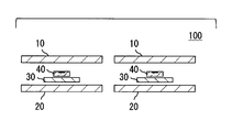
図3は、電流検出システムの変形例を示す断面図であり、
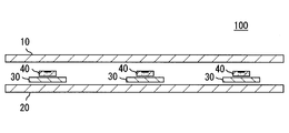
図4は、電流検出システムの変形例を示す断面図であり、
図5は、図3に示す電流検出システムの変形例を示す断面図であり、
図6は、図4に示す電流検出システムの変形例を示す断面図であり、
図7は、磁性板の変形例を示す斜視図であり、
図8は、離間距離を変化させた場合の遮蔽レベルとアスペクト比の関係を示すグラフであり、
図9は、透磁率を変化させた場合の遮蔽レベルとアスペクト比の関係を示すグラフである。
以下、本開示の実施の形態を図に基づいて説明する。
(第1実施形態)
図1および図2に基づいて、本実施形態に係る電流検出システムを説明する。なお、図2においては、煩雑と成ることを避けるために透過空間PSと非透過空間NPS以外の符号を省略している。
(第1実施形態)
図1および図2に基づいて、本実施形態に係る電流検出システムを説明する。なお、図2においては、煩雑と成ることを避けるために透過空間PSと非透過空間NPS以外の符号を省略している。
以下においては互いに直交の関係にある3方向を、x方向、y方向、z方向と示す。そして、x方向とy方向とによって規定される平面をx-y平面、y方向とz方向とによって規定される平面をy-z平面、z方向とx方向とによって規定される平面をz-x平面と示す。x方向は横方向に相当し、y方向は奥行き方向に相当し、z方向は高さ方向に相当する。
図1に示すように、電流検出システム100は、第1磁性板10と、第2磁性板20と、バスバー30と、半導体基板40と、を有する。磁性板10,20は、z方向に所定の間隔を空けて並列配置され、その間に収納空間SSを構成している。この収納空間SS内にバスバー30と半導体基板40とが収納されている。バスバー30はy方向に電流を流し、これによって被測定磁束が形成される。半導体基板40には磁束を電気信号に変換する磁電変換素子41が形成されており、この磁電変換素子41によって被測定磁束が電気信号に変換される。
磁性板10,20それぞれは、空気よりも透磁率の高い材料から成り、収納空間SSへの外部磁束の侵入を抑制するものである。磁性板10,20それぞれは主面がx-y平面に沿う平板形状を成し、z-x平面での断面形状が矩形を成している。そして図1および図2に示すように矩形の短手方向がz方向に沿い、その長手方向がx方向に沿っている。また磁性板10,20それぞれの主面(内面)10a,20aのz方向における離間距離が一定となり、平行の関係と成っている。したがって収納空間SSにおけるz-x平面での断面形状も矩形を成している。
バスバー30には被測定電流が流れる。バスバー30はy方向に延びた棒形状を成し、図1および図2に示すようにz-x平面での断面形状が矩形を成している。そしてその短手方向がz方向に沿い、その長手方向がx方向に沿っている。上記したように被測定電流はy方向に流れる。そのため被測定電流の流動によって、y-z平面を貫く被測定磁束が形成される。この被測定磁束のx成分が磁電変換素子41によって電気信号に変換される。
半導体基板40における第1磁性板10との対向面40aに磁電変換素子41が形成されている。磁電変換素子41は被測定磁束のx方向の成分を電気信号に変換する機能を有する。本実施形態に係る磁電変換素子41は、x方向だけではなく、x-y平面に沿う被測定磁束を電気信号に変換する機能を有する。本実施形態に係る磁電変換素子41は磁束の印加によって抵抗値が変動する磁気抵抗効果素子である。磁電変換素子41は、磁化方向が固定されたピン層と、磁化方向が印加磁界に応じて変動する自由層と、ピン層と自由層との間に設けられた、非磁性の中間層と、を有する。磁電変換素子41はピン層と自由層それぞれの磁化方向の成す角度に応じてその抵抗値が変動する性質を有する。ピン層の磁化方向はx-y平面に沿う一方向に沿っており、自由層の磁化方向はx-y平面でその向きが変動する性質を有する。中間層が導電性を有する場合、磁電変換素子41は巨大磁気抵抗効果素子(GMR)であり、中間層が絶縁性を有する場合、磁電変換素子41はトンネル磁気抵抗効果素子(TMR)である。もちろん、これらに代えて異方性磁気抵抗効果素子(AMR)を採用することもできる。なお、上記した対向面40aが形成面に相当する。
次に電流検出システム100の特徴点を説明する。上記したように磁性板10,20は、z方向に所定の間隔を空けて並列配置され、その間に構成された収納空間SS内にバスバー30と半導体基板40とが収納されている。図2に示すように、x方向に沿う外部磁束が収納空間SSを透過しようとした際、磁性板10,20によってその軌道が曲げられる。そのため収納空間SSは、主として外部磁束の透過する透過空間PS、および、主として外部磁束の透過しない非透過空間NPS(破線で囲まれた空間)に分けられる。ここで、主として外部磁束の透過しない非透過空間NPSの大きさおよびその遮蔽レベルは、どの程度外部磁束を遮蔽するか、という設計者の意向によって定められる。非透過空間NPSの大きさは磁性板10,20それぞれの形成材料、横幅、および、両者のz方向における離間距離(ギャップ)に比例する。そのため、設計者はこれらパラーメータを適宜調整することで、所望の遮蔽レベルと大きさを有する非透過空間NPSを設計することができる。本実施形態では、非透過空間NPSにおける外部磁束の遮蔽レベルが99%以下となるように設定される。その程度の遮蔽が実現されるために、形成材料としてパーマロイ、横幅として20mm、ギャップとして5mmが設定される。なお、上記したように磁性板10,20それぞれは主面がx-y平面に沿う平板形状を成しているので、x方向に沿う外部磁束だけではなく、x-y平面に沿う外部磁束を遮蔽する機能も果たす。
上記した非透過空間NPSに磁電変換素子41が設けられ、バスバー30とz方向にて並んで配置されている。そして収納空間SSの中心CPが非透過空間NPSの中心に位置しており、その中心をx方向に貫く基準線BL(図1に示す一点鎖線)上に、磁電変換素子41の中心が位置している。また、磁電変換素子41およびバスバー30それぞれの幾何学的中心と、磁性板10,20それぞれの幾何学的中心とが、z方向に沿う中心線CL(図1に示す破線)によって貫かれている。さらに言えば、x方向において磁性板10,20それぞれの2つの端部とバスバー30の幾何学的中心との距離が相等しく、磁性板10,20それぞれの2つの端部と磁電変換素子41の幾何学的中心との距離が相等しくなっている。最後に、半導体基板40における磁電変換素子41の形成された対向面40aと第1磁性板10の内面10aとがz方向において互いに対向し、対向面40aと内面10aとの離間距離が一定で、平行の関係になっている。同じく、バスバー30の対向面30aと第2磁性板20の内面20aとの離間距離が一定で、平行の関係となっている。以上により、電流検出システム100はz-x平面において中心線CLを介して線対称の形状を成している。
次に本実施形態に係る電流検出システム100の作用効果を説明する。上記したように、第1磁性板10と第2磁性板20とがz方向に並んでいる。この構成の場合、z方向に直交するx方向の磁束は第1磁性板10と第2磁性板20とによってその軌道が曲げられ、主として外部磁束の透過しない非透過空間NPSが形成される。しかしながらz方向に沿う磁束の場合、その軌道は磁性板によってあまり曲げられず、z方向の成分が一定に保たれる。
したがって本実施形態で示した電流検出システム100とは異なり、収納空間においてバスバーと磁電変換素子とがx方向に並んで配置され、磁電変換素子が被測定磁束におけるz方向の成分を検出する構成の場合、z方向に沿う外部磁束を磁電変換素子が検出するために、バスバーを流れる電流を高精度に検出することがかなわなくなる。これに対して電流検出システム100では、収納空間SSにおいてバスバー30と磁電変換素子41とがz方向に並んで配置され、磁電変換素子41は被測定磁束のx方向の成分を検出する。したがって、上記した比較構成とは異なり、磁電変換素子41はz方向に沿う外部磁束を検出しないので、バスバー30を流れる電流の検出精度の低下が抑制される。
本実施形態では磁電変換素子41が磁気抵抗効果素子である例を示した。しかしながら磁電変換素子41としては上記例に限定されず、磁気信号を電気信号に変換できるものであれば適宜採用することができる。例えば磁電変換素子41としては、x方向に沿う磁束をホール効果によって電圧に変換するホール素子を採用することができる。
本実施形態では、非透過空間NPSにおける外部磁束の遮蔽レベルが99%以下となるように設定される例を示した。しかしながら本実施形態で記したように、外部磁束をどの程度遮蔽するのかは設計者によって決定される事項であって、上記例に限定されない。例えば、遮蔽レベルを90%に採用してもよい。
本実施形態では磁性板10,20それぞれの形成材料がパーマロイ、横幅が20mm、両者の間のギャップが5mmに設定される例を示した。しかしながら磁性板10,20それぞれの形成材料、横幅、および、ギャップそれぞれは遮蔽レベルに応じて適宜変更することができる。磁性板10,20の形成材料としては電磁鋼板、横幅としては30mm、ギャップとしては5mmを採用することもできる。この組み合わせであっても、外部磁束を99%以下に抑えることができる。
本実施形態では磁性板10,20それぞれの厚さ(z方向の長さ)を規定していなかった。磁性板10,20それぞれの厚さは外部磁束や被測定磁束によって磁性板10,20それぞれの内部の磁束が飽和されないように適宜決定される。磁性板10,20それぞれが飽和しなければ、厚さは透過空間PS、非透過空間NPSそれぞれの形成に依存しない。
本実施形態では磁性板10,20それぞれが、x方向に沿う外部磁束だけではなく、x-y平面に沿う外部磁束を遮蔽する例を示した。しかしながら磁電変換素子41がx方向に沿う磁束のみを電気信号に変換する機能を果たす場合、磁性板10,20はx方向に沿う外部磁束のみを遮蔽する機能を果たすだけでも良い。
本実施形態では収納空間SSの中心CPが非透過空間NPSの中心に位置している例を示した。しかしながら両者の中心は一致していなくとも良い。
本実施形態では収納空間SSの中心CPをx方向に貫く基準線BL上に磁電変換素子41の中心が位置している例を示した。しかしながら基準線BL上に磁電変換素子41の中心が位置していなくとも良い。
本実施形態では磁電変換素子41およびバスバー30それぞれの幾何学的中心と、磁性板10,20それぞれの幾何学的中心とが、中心線CLによって貫かれている例を示した。しかしながら磁電変換素子41、バスバー30、および、磁性板10,20それぞれの幾何学的中心が、中心線CLによって貫かれていなくとも良く、z方向において並んでいなくとも良い。
本実施形態では、x方向において、磁性板10,20それぞれの2つの端部とバスバー30の幾何学的中心との距離が相等しく、磁性板10,20それぞれの2つの端部と磁電変換素子41の幾何学的中心との距離が相等しくなっている例を示した。しかしながら、x方向において、磁性板10,20それぞれの2つの端部とバスバー30の幾何学的中心との距離が相異なり、磁性板10,20それぞれの2つの端部と磁電変換素子41の幾何学的中心との距離が相異なっていても良い。
本実施形態では半導体基板40の対向面40aと第1磁性板10の内面10aとの離間距離が一定で、平行の関係になっている例を示した。しかしながら対向面40aと内面10aとの離間距離が不定で、平行の関係になっていなくとも良い。
本実施形態ではバスバー30の対向面30aと第2磁性板20の内面20aとの離間距離が一定で、平行の関係となっている例を示した。しかしながら対向面30aと内面20aとの離間距離が不定で、平行の関係になっていなくとも良い。
本実施形態では電流検出システム100がz-x平面において中心線CLを介して線対称の形状を成している例を示した。しかしながら電流検出システム100は中心線CLを介して線対称の形状を成していなくとも良い。
本実施形態では電流検出システム100が1組の磁性板10,20、これらに対応する1つのバスバー30、および、1つの半導体基板40を有する例を示した。しかしながら磁性板10,20、バスバー30、半導体基板40それぞれの数は限定されない。例えば図3に示すように、電流検出システム100が2組の磁性板10,20、これらに対応する2つのバスバー30、および、2つの半導体基板40を有していても良い。また図4に示すように、電流検出システム100が3組の磁性板10,20、これらに対応する3つのバスバー30、および、3つの半導体基板40を有していても良い。さらに言えば図5に示すように、電流検出システム100が1組の磁性板10,20、これらに対応する2つのバスバー30、および、2つの半導体基板40を有していても良い。最後に図6に示すように、電流検出システム100が1組の磁性板10,20、これらに対応する3つのバスバー30、および、3つの半導体基板40を有していても良い。これにより、部品点数の削減および小型化が可能となる。
本実施形態では磁性板10,20それぞれのx-y平面の形状(以下、平面形状と示す)を特に限定しなかった。磁性板10,20それぞれの平面形状としては特に限定されず、非透過空間NPSを形成できる形状であれば良い。例えばその平面形状としては矩形などの多角形状や円形を採用することができる。図7に、磁性板10,20の平面形状が八角形である例を示す。このように平面形状を円形に近づけることで、x-y平面における外部磁束の遮蔽レベルが均一化される。
上記した各形態において、磁性板10,20それぞれの横幅と離間距離の関係について特に述べていなかった。しかしながら、図1に示すように第1磁性板10における磁電変換素子41と一部が対向する内面10aと、第2磁性板20におけるバスバー30と一部が対向する内面20aとのz方向における離間距離が一定で平行の関係となっている場合、下記に示す関係を満たすと良い。すなわち、内面10aと内面20aとのz方向における離間距離をh、x方向における第1磁性板10および第2磁性板20それぞれの横幅(最長長さ)をwとすると、図8および図9に示すように、離間距離hと横幅wのアスペクト比w/hが4以上である構成が好ましい。
図8は磁性板10,20の離間距離hを3.8~5.6mmまで変えた場合の遮蔽レベルとアスペクト比w/hとの関係を示している。そして図9は磁性板10,20の透磁率をおよそ500~100000Wbまで変えた場合の遮蔽レベルとアスペクト比w/hとの関係を示している。図8に示すように遮蔽レベルは離間距離hに依存せずアスペクト比w/hに依存する。そして図9に示すように遮蔽レベルは透磁率(磁性板10,20の形成材料)によってその値が上下するが、その振る舞いはアスペクト比w/hに依存する。
図8および図9に示すように遮蔽レベルはアスペクト比w/hが4の時に最大となり、そこからアスペクト比w/hが増えるにしたがって徐々に下がる。したがって、上記したようにアスペクト比w/hが4以上の構成が好ましい。なお、外部磁束の遮蔽レベルを例えば88%以上に抑えたい場合、図8および図9に基づくと、アスペクト比w/hを4以上15以下に設定すればよい。アスペクト比w/hの下限値は4で定まるが、上限値はどの程度の遮蔽レベルにするか、という設計者の意向によって決定される。このようにアスペクト比w/hの上限値は設計者の意向によって決定される事項であって、適宜選択可能である。
なお、上記した横幅wは、例えば磁性板10,20の平面形状が円形である場合、その中心を通る直径に相当する。そして、透磁率がおよそ500の材料としてはNi-Znフェライトがあり、透磁率がおよそ1000の材料としては軟鉄がある。また、透磁率がおよそ10000の材料としては電磁鋼板があり、透磁率がおよそ100000の材料としては45%Niパーマロイがある。これら材料の透磁率は作成しているメーカーやそのグレードによって様々に異なる。そのため上記のように、およそ、と記載している。
本開示は、実施例に準拠して記述されたが、本開示は当該実施例や構造に限定されるものではないと理解される。本開示は、様々な変形例や均等範囲内の変形をも包含する。加えて、様々な組み合わせや形態、さらには、それらに一要素のみ、それ以上、あるいはそれ以下、を含む他の組み合わせや形態をも、本開示の範疇や思想範囲に入るものである。
Claims (9)
- 高さ方向に所定の間隔を空けて並列配置された第1磁性板(10)および第2磁性板(20)と、
前記高さ方向に直交する奥行き方向に電流が流れるバスバー(30)と、
前記バスバーを流れる電流によって生じる被測定磁束の前記高さ方向と前記奥行き方向それぞれに直交する横方向の成分を電気信号に変換する磁電変換素子(41)と、を有し、
前記横方向に沿う外部磁束が前記第1磁性板と前記第2磁性板との間に構成された収納空間(SS)を透過しようとした際、前記第1磁性板と前記第2磁性板とによってその軌道が曲げられ、前記収納空間が前記外部磁束の透過する透過空間(PS)、および、前記外部磁束の透過しない非透過空間(NPS)に分けられ、
前記バスバーは前記収納空間に設けられ、
前記磁電変換素子は前記非透過空間に設けられており、
前記バスバーと前記磁電変換素子とは前記高さ方向に並んで配置されている電流検出システム。 - 前記収納空間の中心(CP)を前記横方向に貫く基準線上に、前記磁電変換素子の中心が位置している請求項1に記載の電流検出システム。
- 前記バスバーおよび前記磁電変換素子それぞれの幾何学的中心と、前記第1磁性板および前記第2磁性板それぞれの幾何学的中心とが、前記高さ方向に沿う中心線(CL)によって貫かれている請求項1または請求項2に記載の電流検出システム。
- 前記横方向において、前記第1磁性板および前記第2磁性板それぞれの2つの端部と前記バスバーの幾何学的中心との距離が相等しく、前記第1磁性板および前記第2磁性板それぞれの2つの端部と前記磁電変換素子の幾何学的中心との距離が相等しくなっている請求項3に記載の電流検出システム。
- 前記磁電変換素子が形成された半導体基板(40)を有し、
前記半導体基板における前記磁電変換素子の形成面(40a)と前記第1磁性板の内面(10a)とが前記高さ方向において互いに対向しており、
前記半導体基板の形成面と前記第1磁性板の内面との離間距離が一定であり、前記形成面と前記内面とが平行の関係になっている請求項4に記載の電流検出システム。 - 前記バスバーと前記第2磁性板とが前記高さ方向において互いに対向しており、
前記バスバーにおける前記第2磁性板との対向面(30a)と前記第2磁性板における前記バスバーとの対向面(20a)との離間距離が一定であり、2つの前記対向面が平行の関係となっている請求項4または請求項5に記載の電流検出システム。 - 前記バスバーにおける前記高さ方向と前記横方向とによって規定される平面の断面形状が矩形を成し、その長手方向が前記横方向に沿い、その短手方向が前記高さ方向に沿っている請求項1~6いずれか1項に記載の電流検出システム。
- 前記第1磁性板における前記磁電変換素子と一部が対向する内面(10a)と、前記第2磁性板における前記バスバーと一部が対向する対向面(20a)との前記高さ方向における離間距離が一定で平行の関係となっており、
前記第1磁性板の前記内面と前記第2磁性板の対向面との前記高さ方向における離間距離をh、前記横方向における前記第1磁性板および前記第2磁性板それぞれの最長長さをwとすると、前記離間距離hと前記最長長さwのアスペクト比w/hが4以上である請求項1~7いずれか1項に記載の電流検出システム。 - 前記バスバーは、複数のバスバー部材を有し、
前記磁電変換素子は、複数の磁電変換素子部材を有し、
各バスバー部材には、一つの磁電変換素子部材が対応している請求項1~8のいずれか1項に記載の電流検出システム。
Priority Applications (2)
| Application Number | Priority Date | Filing Date | Title |
|---|---|---|---|
| US15/031,297 US9915685B2 (en) | 2014-01-23 | 2015-01-22 | Electrical current detection system |
| DE112015000490.4T DE112015000490T5 (de) | 2014-01-23 | 2015-01-22 | Stromerfassungssystem |
Applications Claiming Priority (6)
| Application Number | Priority Date | Filing Date | Title |
|---|---|---|---|
| JP2014-010659 | 2014-01-23 | ||
| JP2014010659 | 2014-01-23 | ||
| JP2014070021 | 2014-03-28 | ||
| JP2014-070021 | 2014-03-28 | ||
| JP2015-007086 | 2015-01-16 | ||
| JP2015007086A JP2015194472A (ja) | 2014-01-23 | 2015-01-16 | 電流検出システム |
Publications (1)
| Publication Number | Publication Date |
|---|---|
| WO2015111408A1 true WO2015111408A1 (ja) | 2015-07-30 |
Family
ID=53681218
Family Applications (1)
| Application Number | Title | Priority Date | Filing Date |
|---|---|---|---|
| PCT/JP2015/000283 Ceased WO2015111408A1 (ja) | 2014-01-23 | 2015-01-22 | 電流検出システム |
Country Status (4)
| Country | Link |
|---|---|
| US (1) | US9915685B2 (ja) |
| JP (1) | JP2015194472A (ja) |
| DE (1) | DE112015000490T5 (ja) |
| WO (1) | WO2015111408A1 (ja) |
Cited By (3)
| Publication number | Priority date | Publication date | Assignee | Title |
|---|---|---|---|---|
| JP2017072467A (ja) * | 2015-10-07 | 2017-04-13 | 株式会社デンソー | 電流センサ |
| JP2018096794A (ja) * | 2016-12-12 | 2018-06-21 | 株式会社デンソー | 電流センサ |
| JPWO2023074083A1 (ja) * | 2021-10-29 | 2023-05-04 |
Families Citing this family (20)
| Publication number | Priority date | Publication date | Assignee | Title |
|---|---|---|---|---|
| EP2963428A4 (en) * | 2013-02-27 | 2016-12-28 | Murata Manufacturing Co | CURRENT SENSOR AND ELECTRONIC DEVICE CONTAINING SAME |
| JP6149885B2 (ja) * | 2015-03-18 | 2017-06-21 | トヨタ自動車株式会社 | 電流センサ |
| JP6711086B2 (ja) * | 2016-04-01 | 2020-06-17 | 日立金属株式会社 | 電流センサ |
| US10746821B2 (en) | 2016-06-15 | 2020-08-18 | Denso Corporation | Current sensor |
| JP6690433B2 (ja) * | 2016-06-28 | 2020-04-28 | 日立金属株式会社 | 電流センサ |
| JP6607172B2 (ja) * | 2016-11-17 | 2019-11-20 | 株式会社デンソー | 電流センサ装置 |
| JP2018096795A (ja) * | 2016-12-12 | 2018-06-21 | 株式会社デンソー | 電流センサ |
| JP2018169305A (ja) * | 2017-03-30 | 2018-11-01 | 日立金属株式会社 | 電流センサ |
| JP6973021B2 (ja) * | 2017-12-18 | 2021-11-24 | 日立金属株式会社 | 電流センサ |
| JP7047435B2 (ja) * | 2018-02-13 | 2022-04-05 | 日立金属株式会社 | 電流センサの設計方法 |
| JP7172079B2 (ja) * | 2018-03-20 | 2022-11-16 | 株式会社デンソー | 電流センサ |
| JP2019164075A (ja) * | 2018-03-20 | 2019-09-26 | 株式会社デンソー | 電流センサ |
| JP6919609B2 (ja) | 2018-03-20 | 2021-08-18 | 株式会社デンソー | 電流センサ |
| JP6973221B2 (ja) * | 2018-03-20 | 2021-11-24 | 株式会社デンソー | 電流センサ |
| JP7087512B2 (ja) | 2018-03-20 | 2022-06-21 | 株式会社デンソー | 電流センサ |
| JP6825023B2 (ja) * | 2019-02-27 | 2021-02-03 | 三菱電機株式会社 | 電力変換装置 |
| EP3739345A1 (de) * | 2019-05-16 | 2020-11-18 | Siemens Aktiengesellschaft | Erfassen eines in einer elektrischen leitung fliessenden elektrischen stroms |
| JP7295262B2 (ja) * | 2019-10-08 | 2023-06-20 | アルプスアルパイン株式会社 | 電流検出装置 |
| JP7466646B2 (ja) * | 2020-07-14 | 2024-04-12 | アルプスアルパイン株式会社 | 電流検出装置 |
| DE112023001219T5 (de) * | 2022-03-03 | 2025-01-16 | Asahi Kasei Microdevices Corporation | Stromsensor und Stromerkennungsverfahren |
Citations (3)
| Publication number | Priority date | Publication date | Assignee | Title |
|---|---|---|---|---|
| WO2003038452A1 (en) * | 2001-11-01 | 2003-05-08 | Asahi Kasei Emd Corporation | Current sensor and current sensor manufacturing method |
| JP2005049185A (ja) * | 2003-07-28 | 2005-02-24 | Fuji Electric Holdings Co Ltd | 電流センサのシールド構造 |
| WO2013176271A1 (ja) * | 2012-05-24 | 2013-11-28 | 株式会社フジクラ | 電流センサ |
Family Cites Families (14)
| Publication number | Priority date | Publication date | Assignee | Title |
|---|---|---|---|---|
| EP0996083B1 (en) | 1992-09-28 | 2003-03-26 | Olympus Optical Co., Ltd. | Information reproducing system for optically reading a dot code from a recording medium |
| JP2988874B2 (ja) * | 1996-09-05 | 1999-12-13 | 日立造船株式会社 | ツインロール式連続鋳造機 |
| JP3647736B2 (ja) * | 2000-09-29 | 2005-05-18 | 株式会社東芝 | 磁気抵抗効果素子、磁気ヘッド及び磁気再生装置 |
| JP2003309393A (ja) * | 2002-04-12 | 2003-10-31 | Fujita Corp | 磁気シールド構造およびその設計法 |
| US7106046B2 (en) * | 2002-06-18 | 2006-09-12 | Asahi Kasei Emd Corporation | Current measuring method and current measuring device |
| JP4773787B2 (ja) * | 2005-09-27 | 2011-09-14 | 株式会社ハネックス | データキャリア構造及びその設置構造 |
| EP1811311B1 (de) * | 2006-01-19 | 2016-08-31 | Melexis Technologies NV | Vorrichtung zur Strommessung |
| JP5263494B2 (ja) | 2008-06-19 | 2013-08-14 | Tdk株式会社 | 電流センサ |
| JP2010133737A (ja) * | 2008-12-02 | 2010-06-17 | Denso Corp | 電流センサ装置、及び電流センサ自己診断装置 |
| JP5482736B2 (ja) * | 2011-06-28 | 2014-05-07 | 株式会社デンソー | 電流センサ |
| JP2013101840A (ja) * | 2011-11-09 | 2013-05-23 | Canon Inc | 荷電粒子線装置、それを用いた物品の製造方法 |
| JP2013113631A (ja) | 2011-11-25 | 2013-06-10 | Yazaki Corp | 電流検出装置 |
| JP2013238580A (ja) * | 2011-12-28 | 2013-11-28 | Tdk Corp | 電流センサ |
| JP2013246005A (ja) * | 2012-05-24 | 2013-12-09 | Fujikura Ltd | 電流センサ |
-
2015
- 2015-01-16 JP JP2015007086A patent/JP2015194472A/ja active Pending
- 2015-01-22 DE DE112015000490.4T patent/DE112015000490T5/de not_active Withdrawn
- 2015-01-22 US US15/031,297 patent/US9915685B2/en active Active
- 2015-01-22 WO PCT/JP2015/000283 patent/WO2015111408A1/ja not_active Ceased
Patent Citations (3)
| Publication number | Priority date | Publication date | Assignee | Title |
|---|---|---|---|---|
| WO2003038452A1 (en) * | 2001-11-01 | 2003-05-08 | Asahi Kasei Emd Corporation | Current sensor and current sensor manufacturing method |
| JP2005049185A (ja) * | 2003-07-28 | 2005-02-24 | Fuji Electric Holdings Co Ltd | 電流センサのシールド構造 |
| WO2013176271A1 (ja) * | 2012-05-24 | 2013-11-28 | 株式会社フジクラ | 電流センサ |
Cited By (5)
| Publication number | Priority date | Publication date | Assignee | Title |
|---|---|---|---|---|
| JP2017072467A (ja) * | 2015-10-07 | 2017-04-13 | 株式会社デンソー | 電流センサ |
| JP2018096794A (ja) * | 2016-12-12 | 2018-06-21 | 株式会社デンソー | 電流センサ |
| WO2018110108A1 (ja) * | 2016-12-12 | 2018-06-21 | 株式会社デンソー | 電流センサ |
| JPWO2023074083A1 (ja) * | 2021-10-29 | 2023-05-04 | ||
| JP7615344B2 (ja) | 2021-10-29 | 2025-01-16 | アルプスアルパイン株式会社 | 電流センサ |
Also Published As
| Publication number | Publication date |
|---|---|
| JP2015194472A (ja) | 2015-11-05 |
| US20160258985A1 (en) | 2016-09-08 |
| US9915685B2 (en) | 2018-03-13 |
| DE112015000490T5 (de) | 2016-11-10 |
Similar Documents
| Publication | Publication Date | Title |
|---|---|---|
| WO2015111408A1 (ja) | 電流検出システム | |
| US9644994B2 (en) | Magnetic sensor | |
| CN107976644B (zh) | 磁场检测装置 | |
| US9417269B2 (en) | Current sensor | |
| CN107561460B (zh) | 磁传感器装置和磁感测方法 | |
| JP4837749B2 (ja) | 磁気センサ及びそれを用いた磁気エンコーダ | |
| JP6305181B2 (ja) | 磁気センサ | |
| JP6107942B2 (ja) | 磁気電流センサおよび電流測定方法 | |
| JP5899012B2 (ja) | 磁気センサ | |
| JP6503802B2 (ja) | 磁気センサ | |
| CN108152762B (zh) | 磁场检测装置 | |
| JP2009300150A (ja) | 磁気センサ及び磁気センサモジュール | |
| JP2013210335A (ja) | 磁気センサ | |
| US10254305B2 (en) | Inertial sensor | |
| JP6121311B2 (ja) | 磁気検知装置 | |
| US10830838B2 (en) | Magnetic sensor | |
| JP2014089088A (ja) | 磁気抵抗効果素子 | |
| JP2015135267A (ja) | 電流センサ | |
| WO2011074488A1 (ja) | 磁気センサ | |
| CN109541503B (zh) | 磁传感器 | |
| JP2019138807A (ja) | 磁気センサおよび電流センサ | |
| US9753100B2 (en) | Magnetic sensor | |
| JP2018096895A (ja) | 磁場検出装置 | |
| WO2014045559A1 (ja) | 電流センサ | |
| JP2019087688A (ja) | 磁気センサ |
Legal Events
| Date | Code | Title | Description |
|---|---|---|---|
| 121 | Ep: the epo has been informed by wipo that ep was designated in this application |
Ref document number: 15739918 Country of ref document: EP Kind code of ref document: A1 |
|
| WWE | Wipo information: entry into national phase |
Ref document number: 15031297 Country of ref document: US |
|
| WWE | Wipo information: entry into national phase |
Ref document number: 112015000490 Country of ref document: DE |
|
| 122 | Ep: pct application non-entry in european phase |
Ref document number: 15739918 Country of ref document: EP Kind code of ref document: A1 |