WO2015108024A1 - 半導体装置、固体撮像装置、および撮像装置 - Google Patents
半導体装置、固体撮像装置、および撮像装置 Download PDFInfo
- Publication number
- WO2015108024A1 WO2015108024A1 PCT/JP2015/050617 JP2015050617W WO2015108024A1 WO 2015108024 A1 WO2015108024 A1 WO 2015108024A1 JP 2015050617 W JP2015050617 W JP 2015050617W WO 2015108024 A1 WO2015108024 A1 WO 2015108024A1
- Authority
- WO
- WIPO (PCT)
- Prior art keywords
- substrate
- opening
- substrates
- semiconductor layer
- wiring
- Prior art date
- Legal status (The legal status is an assumption and is not a legal conclusion. Google has not performed a legal analysis and makes no representation as to the accuracy of the status listed.)
- Ceased
Links
Images


Classifications
-
- H—ELECTRICITY
- H10—SEMICONDUCTOR DEVICES; ELECTRIC SOLID-STATE DEVICES NOT OTHERWISE PROVIDED FOR
- H10F—INORGANIC SEMICONDUCTOR DEVICES SENSITIVE TO INFRARED RADIATION, LIGHT, ELECTROMAGNETIC RADIATION OF SHORTER WAVELENGTH OR CORPUSCULAR RADIATION
- H10F39/00—Integrated devices, or assemblies of multiple devices, comprising at least one element covered by group H10F30/00, e.g. radiation detectors comprising photodiode arrays
- H10F39/80—Constructional details of image sensors
- H10F39/809—Constructional details of image sensors of hybrid image sensors
-
- H—ELECTRICITY
- H04—ELECTRIC COMMUNICATION TECHNIQUE
- H04N—PICTORIAL COMMUNICATION, e.g. TELEVISION
- H04N25/00—Circuitry of solid-state image sensors [SSIS]; Control thereof
-
- H—ELECTRICITY
- H04—ELECTRIC COMMUNICATION TECHNIQUE
- H04N—PICTORIAL COMMUNICATION, e.g. TELEVISION
- H04N25/00—Circuitry of solid-state image sensors [SSIS]; Control thereof
- H04N25/70—SSIS architectures; Circuits associated therewith
- H04N25/76—Addressed sensors, e.g. MOS or CMOS sensors
-
- H—ELECTRICITY
- H04—ELECTRIC COMMUNICATION TECHNIQUE
- H04N—PICTORIAL COMMUNICATION, e.g. TELEVISION
- H04N25/00—Circuitry of solid-state image sensors [SSIS]; Control thereof
- H04N25/70—SSIS architectures; Circuits associated therewith
- H04N25/76—Addressed sensors, e.g. MOS or CMOS sensors
- H04N25/78—Readout circuits for addressed sensors, e.g. output amplifiers or A/D converters
-
- H—ELECTRICITY
- H10—SEMICONDUCTOR DEVICES; ELECTRIC SOLID-STATE DEVICES NOT OTHERWISE PROVIDED FOR
- H10F—INORGANIC SEMICONDUCTOR DEVICES SENSITIVE TO INFRARED RADIATION, LIGHT, ELECTROMAGNETIC RADIATION OF SHORTER WAVELENGTH OR CORPUSCULAR RADIATION
- H10F39/00—Integrated devices, or assemblies of multiple devices, comprising at least one element covered by group H10F30/00, e.g. radiation detectors comprising photodiode arrays
- H10F39/80—Constructional details of image sensors
- H10F39/804—Containers or encapsulations
-
- H—ELECTRICITY
- H10—SEMICONDUCTOR DEVICES; ELECTRIC SOLID-STATE DEVICES NOT OTHERWISE PROVIDED FOR
- H10F—INORGANIC SEMICONDUCTOR DEVICES SENSITIVE TO INFRARED RADIATION, LIGHT, ELECTROMAGNETIC RADIATION OF SHORTER WAVELENGTH OR CORPUSCULAR RADIATION
- H10F39/00—Integrated devices, or assemblies of multiple devices, comprising at least one element covered by group H10F30/00, e.g. radiation detectors comprising photodiode arrays
- H10F39/80—Constructional details of image sensors
- H10F39/811—Interconnections
-
- H—ELECTRICITY
- H10—SEMICONDUCTOR DEVICES; ELECTRIC SOLID-STATE DEVICES NOT OTHERWISE PROVIDED FOR
- H10F—INORGANIC SEMICONDUCTOR DEVICES SENSITIVE TO INFRARED RADIATION, LIGHT, ELECTROMAGNETIC RADIATION OF SHORTER WAVELENGTH OR CORPUSCULAR RADIATION
- H10F99/00—Subject matter not provided for in other groups of this subclass
-
- H—ELECTRICITY
- H10—SEMICONDUCTOR DEVICES; ELECTRIC SOLID-STATE DEVICES NOT OTHERWISE PROVIDED FOR
- H10W—GENERIC PACKAGES, INTERCONNECTIONS, CONNECTORS OR OTHER CONSTRUCTIONAL DETAILS OF DEVICES COVERED BY CLASS H10
- H10W20/00—Interconnections in chips, wafers or substrates
- H10W20/40—Interconnections external to wafers or substrates, e.g. back-end-of-line [BEOL] metallisations or vias connecting to gate electrodes
-
- H—ELECTRICITY
- H10—SEMICONDUCTOR DEVICES; ELECTRIC SOLID-STATE DEVICES NOT OTHERWISE PROVIDED FOR
- H10W—GENERIC PACKAGES, INTERCONNECTIONS, CONNECTORS OR OTHER CONSTRUCTIONAL DETAILS OF DEVICES COVERED BY CLASS H10
- H10W72/00—Interconnections or connectors in packages
- H10W72/50—Bond wires
- H10W72/531—Shapes of wire connectors
- H10W72/536—Shapes of wire connectors the connected ends being ball-shaped
-
- H—ELECTRICITY
- H10—SEMICONDUCTOR DEVICES; ELECTRIC SOLID-STATE DEVICES NOT OTHERWISE PROVIDED FOR
- H10W—GENERIC PACKAGES, INTERCONNECTIONS, CONNECTORS OR OTHER CONSTRUCTIONAL DETAILS OF DEVICES COVERED BY CLASS H10
- H10W72/00—Interconnections or connectors in packages
- H10W72/50—Bond wires
- H10W72/531—Shapes of wire connectors
- H10W72/5366—Shapes of wire connectors the bond wires having kinks
-
- H—ELECTRICITY
- H10—SEMICONDUCTOR DEVICES; ELECTRIC SOLID-STATE DEVICES NOT OTHERWISE PROVIDED FOR
- H10W—GENERIC PACKAGES, INTERCONNECTIONS, CONNECTORS OR OTHER CONSTRUCTIONAL DETAILS OF DEVICES COVERED BY CLASS H10
- H10W72/00—Interconnections or connectors in packages
- H10W72/50—Bond wires
- H10W72/59—Bond pads specially adapted therefor
-
- H—ELECTRICITY
- H10—SEMICONDUCTOR DEVICES; ELECTRIC SOLID-STATE DEVICES NOT OTHERWISE PROVIDED FOR
- H10W—GENERIC PACKAGES, INTERCONNECTIONS, CONNECTORS OR OTHER CONSTRUCTIONAL DETAILS OF DEVICES COVERED BY CLASS H10
- H10W72/00—Interconnections or connectors in packages
- H10W72/90—Bond pads, in general
- H10W72/921—Structures or relative sizes of bond pads
- H10W72/923—Bond pads having multiple stacked layers
- H10W72/9232—Bond pads having multiple stacked layers with additional elements interposed between layers
-
- H—ELECTRICITY
- H10—SEMICONDUCTOR DEVICES; ELECTRIC SOLID-STATE DEVICES NOT OTHERWISE PROVIDED FOR
- H10W—GENERIC PACKAGES, INTERCONNECTIONS, CONNECTORS OR OTHER CONSTRUCTIONAL DETAILS OF DEVICES COVERED BY CLASS H10
- H10W72/00—Interconnections or connectors in packages
- H10W72/90—Bond pads, in general
- H10W72/931—Shapes of bond pads
- H10W72/932—Plan-view shape, i.e. in top view
-
- H—ELECTRICITY
- H10—SEMICONDUCTOR DEVICES; ELECTRIC SOLID-STATE DEVICES NOT OTHERWISE PROVIDED FOR
- H10W—GENERIC PACKAGES, INTERCONNECTIONS, CONNECTORS OR OTHER CONSTRUCTIONAL DETAILS OF DEVICES COVERED BY CLASS H10
- H10W72/00—Interconnections or connectors in packages
- H10W72/90—Bond pads, in general
- H10W72/981—Auxiliary members, e.g. spacers
- H10W72/983—Reinforcing structures, e.g. collars
Definitions
- the present invention relates to a semiconductor device, a solid-state imaging device, and an imaging device having a plurality of stacked (stacked) substrates.
- a device having a structure in which a plurality of substrates having a semiconductor layer (including a case where the semiconductor layer is a supporting substrate) and a wiring layer are overlapped (laminated) is known.
- a solid-state imaging device described in Patent Document 1 an opening is formed in the semiconductor layer of the substrate disposed on the uppermost side, and the wiring layer is exposed.
- the portion where the opening is formed functions as a pad for electrical connection with the outside.
- wire bonding In wire bonding, a metal wire is connected to the wiring layer exposed by forming the opening.
- the shape of the opening is generally a quadrangle. Further, in an apparatus having a structure in which a plurality of substrates are overlapped, generally, resin is injected between them in order to increase the bonding strength between two adjacent substrates.
- the elastic modulus of the resin is lower than the elastic modulus of the wiring layer, it is difficult for the ultrasonic wave applied during wire bonding to be transmitted to the connection between the wire and the wiring layer, and the output and load of the ultrasonic wave must be increased. In this case, connection failure occurs between the wire and the wiring layer.
- wire bonding if wire bonding is performed, if the output of ultrasonic waves or the load is increased, the stress is concentrated at the corners of the quadrilateral because the shape of the opening is quadrangular. As a result, cracks are likely to occur in the semiconductor layer starting from the corner.
- the present invention provides a technique capable of suppressing the occurrence of cracks.
- a semiconductor device includes a plurality of substrates each having a semiconductor layer and a wiring layer formed with wiring for transmitting a signal and overlapping the semiconductor layer, each substrate being The wiring of the edge substrate between the semiconductor layer of the edge substrate, which is a substrate located at one of both ends of the plurality of substrates, and which overlaps in a direction crossing the main surface, and the substrate adjacent to the edge substrate A plurality of substrates on which a layer is disposed; a connection part that electrically connects two adjacent substrates of the plurality of substrates; and a substrate disposed between two adjacent substrates of the plurality of substrates, A resin layer covering at least a part of the surface of the connection portion, and a first opening formed in the semiconductor layer of the edge substrate and exposing the wiring layer of the edge substrate, the main surface of the edge substrate Shape seen in the direction directly opposite It has a first opening which is polygonal or circular over pentagon, a.
- the first opening when viewed in a direction facing the main surface of the edge substrate, is formed from the center of the first opening.
- the distance to each of the plurality of corners of the opening may be the same.
- the regular polygonal shape in which the shape of the first opening viewed in the direction facing the main surface of the edge substrate is a pentagon or more. It may be.
- the wiring layer of the edge substrate is formed so as to at least partially overlap the first opening, and the wiring The second opening may be a polygon having a pentagon or more or a circle when viewed in a direction facing the main surface of the edge substrate.
- all internal angles of the polygon may be 90 degrees or more.
- a solid-state imaging device includes the semiconductor device according to the first aspect, and a photoelectric conversion unit that converts light into a signal is provided in the semiconductor layer of the edge substrate.
- a signal processing unit for processing a signal generated by the photoelectric conversion unit is formed in the semiconductor layer and the wiring layer formed on a substrate different from the edge substrate.
- a solid-state imaging device includes the semiconductor device according to the first aspect, and converts light into a signal in the semiconductor layer on a substrate different from the edge substrate.
- a photoelectric conversion unit is formed, and a signal processing unit that processes a signal generated by the photoelectric conversion unit is formed in the semiconductor layer and the wiring layer of the edge substrate.
- an imaging device includes the solid-state imaging device according to the sixth aspect or the seventh aspect.
- the shape of the first opening seen in the direction facing the main surface of the edge substrate is a polygon or a circle of pentagon or more, the occurrence of cracks can be suppressed.
- FIG. 1 It is sectional drawing which shows the structural example of the solid-state imaging device by the 1st Embodiment of this invention. It is a top view which shows the shape of the opening part of the solid-state imaging device by the 1st Embodiment of this invention. It is a top view which shows the shape of the opening part of the solid-state imaging device by the 1st Embodiment of this invention. It is a top view which shows the shape of the opening part of the solid-state imaging device by the 1st Embodiment of this invention. It is a top view which shows the shape of the opening part of the solid-state imaging device by the 1st Embodiment of this invention.
- FIG. 1 is a block diagram illustrating an example of the overall configuration of a solid-state imaging device according to a first embodiment of the present invention. It is sectional drawing which shows the structural example of the solid-state imaging device by the 2nd Embodiment of this invention. It is a block diagram which shows the structural example of the imaging device by the 3rd Embodiment of this invention.
- FIG. 1 shows a configuration example of the solid-state imaging device according to the present embodiment.
- FIG. 1 shows a cross section of the solid-state imaging device.
- the solid-state imaging device illustrated in FIG. 1 includes a plurality of stacked (laminated) substrates (first substrate 10 and second substrate 20), a connection unit 30, and a resin layer 40.
- the dimensions of the parts constituting the solid-state imaging device shown in FIG. 1 do not follow the dimensions shown in FIG.
- the dimension of the part which comprises the solid-state imaging device shown in FIG. 1 may be arbitrary.
- the ratio of dimensions of each component is appropriately changed in order to make the drawings easy to see.
- the first substrate 10 and the second substrate 20 are separated in a direction (for example, a direction substantially perpendicular to the main surface) across the main surface (the widest surface among a plurality of surfaces constituting the surface of the substrate) of each substrate. Are overlapping.
- the first substrate 10 has a semiconductor layer 100 and a wiring layer 110.
- the semiconductor layer 100 and the wiring layer 110 overlap each other in a direction crossing the main surface of the first substrate 10 (for example, a direction substantially perpendicular to the main surface). Further, the semiconductor layer 100 and the wiring layer 110 are in contact with each other.
- the semiconductor layer 100 includes a photoelectric conversion unit 101 that converts incident light into a signal.
- the semiconductor layer 100 is made of a material containing a semiconductor such as silicon (Si).
- the photoelectric conversion unit 101 is made of, for example, a semiconductor material having an impurity concentration different from that of the semiconductor material forming the semiconductor layer 100.
- the semiconductor layer 100 has a first surface that is in contact with the wiring layer 110 and a second surface that is opposite to the first surface and exposed to the outside. Light incident on the second surface of the semiconductor layer 100 travels through the semiconductor layer 100 and enters the photoelectric conversion unit 101.
- the solid-state imaging device has a plurality of photoelectric conversion units 101.
- photoelectric conversion units 101 In FIG. 1, four photoelectric conversion units 101 are shown.
- symbol of one photoelectric conversion part 101 is shown as a representative.
- the plurality of photoelectric conversion units 101 When viewed in a direction facing the main surface of the first substrate 10, that is, when the first substrate 10 is viewed in plan, the plurality of photoelectric conversion units 101 are arranged in a matrix.
- the wiring layer 110 includes a wiring 111 and a via 112.
- the wiring 111 transmits a signal generated by the photoelectric conversion unit 101 and other signals.
- the via 112 connects the wirings 111 of different layers. In FIG. 1, there are a plurality of wirings 111, but a symbol of one wiring 111 is shown as a representative. In FIG. 1, there are a plurality of vias 112, but a symbol of one via 112 is shown as a representative.
- the wiring 111 is made of a conductive material (for example, a metal such as aluminum (Al) or copper (Cu)).
- the wiring layer 110 has a first surface that is in contact with the resin layer 40 and a second surface that is on the opposite side of the first surface and is in contact with the semiconductor layer 100.
- the wiring 111 is a thin film on which a wiring pattern is formed. Only one layer of wiring 111 may be formed, or a plurality of layers of wiring 111 may be formed. In the example shown in FIG. 1, six layers of wiring 111 are formed. The wirings 111 of different layers are connected by vias 112. The via 112 is made of a conductive material. In the wiring layer 110, portions other than the wiring 111 and the via 112 are made of an interlayer insulating film such as silicon dioxide (SiO 2 ).
- the second substrate 20 includes a semiconductor layer 200 and a wiring layer 210.
- the semiconductor layer 200 and the wiring layer 210 overlap each other in a direction crossing the main surface of the second substrate 20 (for example, a direction substantially perpendicular to the main surface). Further, the semiconductor layer 200 and the wiring layer 210 are in contact with each other.
- the semiconductor layer 200 functions as a support substrate.
- the semiconductor layer 200 is made of a material containing a semiconductor such as silicon (Si).
- the semiconductor layer 200 has a first surface that is in contact with the wiring layer 210 and a second surface that is opposite to the first surface and exposed to the outside.
- the wiring layer 210 includes a wiring 211 and a via 212.
- the wiring 211 transmits a signal generated by the photoelectric conversion unit 101 of the first substrate 10 and other signals.
- the via 212 connects wirings 211 of different layers. In FIG. 1, there are a plurality of wirings 211, but a symbol of one wiring 211 is shown as a representative. In FIG. 1, there are a plurality of vias 212, but a symbol of one via 212 is shown as a representative.
- the wiring 211 is made of a conductive material (for example, a metal such as aluminum (Al) or copper (Cu)).
- the wiring layer 210 has a first surface that is in contact with the resin layer 40, and a second surface that is on the opposite side of the first surface and is in contact with the semiconductor layer 200.
- the wiring 211 is a thin film on which a wiring pattern is formed. Only one layer of wiring 211 may be formed, or multiple layers of wiring 211 may be formed. In the example shown in FIG. 1, six layers of wirings 211 are formed. Wirings 211 of different layers are connected by vias 212.
- the via 212 is made of a conductive material.
- portions other than the wiring 211 and the via 212 are formed of an interlayer insulating film such as silicon dioxide (SiO 2 ).
- connection unit 30 is disposed between two adjacent substrates of the plurality of substrates included in the solid-state imaging device, and electrically connects the two substrates.
- the connection unit 30 is disposed between the first substrate 10 and the second substrate 20 and electrically connects the first substrate 10 and the second substrate 20.
- the connection portion 30 is made of a conductive material (for example, a metal such as gold (Au) or copper (Cu)).
- the connection unit 30 includes connection electrodes 300 and 301 and bumps 302.
- the connection electrode 300 is connected to the via 112 of the wiring layer 110.
- the connection electrode 301 is connected to the via 212 of the wiring layer 210.
- At least a part of the surface of the connection portion 30 is covered with the resin layer 40.
- At least a part of the surface of the connecting portion 30 described above is the surface of the connecting portion 30 excluding the surface in contact with the wiring layer 110 and the surface in contact with the wiring layer 210.
- the resin layer 40 is disposed between two adjacent substrates of a plurality of substrates included in the solid-state imaging device, and connects the two substrates.
- the resin layer 40 is disposed between the first substrate 10 and the second substrate 20 and connects the first substrate 10 and the second substrate 20.
- the resin layer 40 is made of, for example, an epoxy resin. By the resin layer 40, the bonding strength between the substrates is further increased.
- the first substrate 10 and the second substrate 20 are connected via the resin layer 40 with the wiring layer 110 of the first substrate 10 and the wiring layer 210 of the second substrate 20 facing each other. .
- the resin layer 40 is in contact with the first surface of the wiring layer 110 and the first surface of the wiring layer 210.
- the resin layer 40 covers at least a part of the surface of the connection portion 30.
- an opening 500 is formed in a pad region 50 for electrical connection with the outside.
- the wiring layer 110 in the pad region 50 is exposed.
- the uppermost wiring 111 of the wiring layer 110 is exposed.
- the opening 500 includes the sidewall of the semiconductor layer 100 and the sidewall of the wiring layer 110.
- the side wall of the semiconductor layer 100 is exposed by forming a hole penetrating the semiconductor layer 100.
- the side wall of the wiring layer 110 is exposed by forming a groove in the wiring layer 110. That is, the opening 500 includes a first opening 501 and a second opening 502.
- the first opening 501 is formed in the semiconductor layer 100 so as to expose the wiring layer 110.
- the second opening 502 is formed on the wiring layer 110 so as to at least partly overlap the first opening 501 and to expose the wiring 111.
- the exposed wiring 111 functions as a pad which is an electrode electrically connected to the outside.
- a wire 60 is connected to the wiring 111 by wire bonding.
- the second opening 502 may not be formed. Therefore, in the present embodiment, the second opening 502 is not an essential structure.
- the first substrate 10 and the second substrate 20 are electrically connected by the connection portion 30 including the bump 302, but the connection portion that electrically connects two adjacent substrates is used.
- the mounting method is not limited to the method shown in the present embodiment.
- two adjacent substrates may be electrically connected by a through silicon via (TSV: Through-Silicon Via).
- TSV Through-Silicon Via
- the adjacent two substrates may be electrically connected by directly bonding the connection electrodes formed on the two adjacent substrates without forming bumps.
- the solid-state imaging device shown in FIG. 1 has two substrates, the solid-state imaging device may have three or more substrates.
- Each of the plurality of substrates included in the solid-state imaging device may have a semiconductor layer and a wiring layer.
- the substrate located at either end of the plurality of substrates included in the solid-state imaging device is an edge substrate.
- the wiring layer of the edge substrate may be disposed between the semiconductor layer of the edge substrate and the substrate adjacent to the edge substrate.
- the edge substrate is a substrate disposed on the outermost side among the plurality of substrates, and has a main surface that is not in contact with other substrates among the plurality of substrates.
- the edge substrate is arranged on the uppermost side or the lowermost side of the plurality of substrates when the plurality of substrates are arranged such that at least one main surface of the plurality of substrates is substantially parallel to the horizontal plane.
- Substrate When the solid-state imaging device has two substrates, one of the two substrates is an edge substrate. In the solid-state imaging device shown in FIG. 1, the first substrate 10 is an edge substrate.
- the semiconductor layer included in the edge substrate may be disposed outside the wiring layer included in the edge substrate.
- the photoelectric conversion part which converts light into a signal should just be formed in the semiconductor layer of an edge board
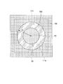
- FIG. 2 shows the shape of the opening 500 when viewed in a direction directly opposite to the main surface of the first substrate 10 (a direction substantially perpendicular to the main surface of the first substrate 10), that is, a plan view of the opening 500. The shape is shown.
- an opening 500 is formed in the semiconductor layer 100, and the surface 111a of the wiring 111 is exposed.
- a wire 60 is connected to the center of the surface 111a of the exposed wiring 111.
- the shape of the opening 500 is a regular octagon.
- the opening 500 has eight corners located at the apexes of a regular octagon and eight straight portions that are sides of the regular octagon.
- the center P1 of the opening 500 is at the intersection of the vertical bisectors of the eight straight lines.
- the distance D1 from the center P1 to the corner C1 and the distance D2 from the center P1 to the corner C2 are the same.
- the distances from the center P1 to each of the remaining six corners are also the same as the distances D1 and D2. Since the distance from the center P1 to the corner is the same, the deflection of the semiconductor layer 100 during wire bonding becomes uniform, and the stress at the corner can be made uniform. Thereby, generation
- the center P1 may be the center of gravity of the opening 500.
- the shape of the first opening 501 formed in the semiconductor layer 100 and constituting the opening 500 is the same as the shape of the second opening 502 formed in the wiring layer 110.
- Only the shape of the first opening 501 may be a regular octagon.
- the shape of the first opening 501 to a regular octagon, the occurrence of cracks in the semiconductor layer 100 due to the stress generated in the semiconductor layer 100 during wire bonding can be suppressed.
- the shape of the second opening 502 By setting the shape of the second opening 502 to a regular octagon, generation of cracks in the wiring layer 110 due to stress generated in the wiring layer 110 during wire bonding can be suppressed.
- the shape of the opening 500 may be a polygon other than a regular octagon. 3, 4, and 5 show other shapes of the opening 500 when viewed in the direction facing the main surface of the first substrate 10. 3, 4, and 5, an opening 500 is formed in the semiconductor layer 100, and the surface 111 a of the wiring 111 is exposed. A wire 60 is connected to the center of the exposed surface 111a of the wiring 111.
- the shape of the opening 500 is a regular pentagon.
- the shape of the opening 500 is a regular hexagon.
- the shape of the opening 500 is a regular heptagon. Regardless of whether the shape of the opening 500 is a regular pentagon, a regular hexagon, or a regular heptagon, the occurrence of cracks can be suppressed by increasing the number of corners compared to the prior art. Moreover, even if the shape of the opening 500 is any of a regular pentagon, a regular hexagon, and a regular heptagon, the occurrence of cracks can be suppressed because the distance from the center to the corner is the same.
- the shape of the opening 500 may be a polygon that is a pentagon or more. Polygonal corners forming the opening 500 may be rounded. The polygon which comprises the opening part 500 should just have five or more linear parts from which a direction differs mutually. The polygon that forms the opening 500 may not be a regular polygon. The distance from the center of the opening 500 to each of the plurality of corners of the opening 500 is preferably the same. It is desirable that all the internal angles of the polygon forming the opening 500 are 90 degrees or more.
- the shape of the opening 500 may be a circle.
- FIG. 6 shows the shape of the opening 500 when viewed in the direction facing the main surface of the first substrate 10.
- the shape of the opening 500 is a circle.
- the distance D3 from the center P2 of the opening 500 to the periphery of the opening 500 is uniform. Since the distance from the center P2 to the periphery of the opening 500 is uniform, the deflection of the semiconductor layer 100 during wire bonding is uniform, and the stress generated on the periphery of the opening 500 can be controlled uniformly. it can. Thereby, generation
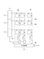
- FIG. 7 shows an example of the overall configuration of the solid-state imaging device.
- the solid-state imaging device shown in FIG. 7 includes a pixel unit 70 (pixel array), a vertical scanning circuit 71, a column processing circuit 72, a horizontal scanning circuit 73, and an output amplifier 74.
- the arrangement position of each circuit element shown in FIG. 7 does not necessarily coincide with the actual arrangement position.
- the pixel unit 70 includes pixels 700 arranged in a two-dimensional matrix and a current source 701 provided for each column.
- the pixel 700 includes the photoelectric conversion unit 101 illustrated in FIG.
- the vertical scanning circuit 71 controls the driving of the pixel unit 70 in units of rows. In order to perform this drive control, the vertical scanning circuit 71 is composed of unit circuits 71-1, 71-2,..., 71-n (n is the number of rows) as many as the number of rows.
- the signal line 702 is connected to the pixel 700, and supplies the control signal output from the unit circuit 71-i to the pixel 700.
- each signal line 702 corresponding to each row is represented by one line, but each signal line 702 includes a plurality of signal lines.
- the signal of the pixel 700 in the row selected by the control signal is output to the vertical signal line 703 provided for each column.
- the current source 701 is connected to the vertical signal line 703 and constitutes an amplification transistor and a source follower circuit in the pixel 700.
- the column processing circuit 72 performs signal processing such as noise suppression on the pixel signal output to the vertical signal line 703.
- the horizontal scanning circuit 73 outputs the pixel signals of the pixels 700 for one row output to the vertical signal line 703 and processed by the column processing circuit 72 to the output amplifier 74 in time series.
- the output amplifier 74 amplifies the pixel signal output from the horizontal scanning circuit 73 and outputs it as an image signal to the outside of the solid-state imaging device.
- the pixel unit 70 is disposed on the first substrate 10.
- the vertical scanning circuit 71, the horizontal scanning circuit 73, and the output amplifier 74 may be disposed on either the first substrate 10 or the second substrate 20, respectively.
- the column processing circuit 72 is a signal processing unit that processes a signal generated by the photoelectric conversion unit 101.
- the column processing circuit 72 is formed on the semiconductor layer 200 and the wiring layer 210 of the second substrate 20 different from the first substrate 10 on which the photoelectric conversion unit 101 is formed.
- the present invention is applied to a solid-state imaging device having a photoelectric conversion unit.
- the present invention is applied to a semiconductor device having a plurality of substrates each having a semiconductor layer and a wiring layer. Is possible.
- a plurality of substrates having semiconductor layers 100 and 200 and wiring layers 110 and 210 that are formed with wirings 111 and 211 for transmitting signals and overlap the semiconductor layers 100 and 200.
- the second substrate 20) of the edge substrate which is a substrate located on either of both ends of the plurality of substrates, with each substrate overlapping in a direction crossing the main surface.
- a plurality of substrates in which the wiring layer 110 of the edge substrate is disposed between the semiconductor layer 100 and a substrate adjacent to the edge substrate (second substrate 20), and two adjacent substrates of the plurality of substrates are electrically connected Formed in the semiconductor layer 100 of the edge substrate, the resin layer 40 that is disposed between the two adjacent substrates of the plurality of substrates, the resin layer 40 that covers at least a part of the surface of the connection unit 30, Edge board wiring layer And a first opening 501 that exposes 10 and has a first opening 501 that is a polygon or a circle of a pentagon or more in a direction facing the main surface of the edge substrate. Composed.
- the shape of the first opening 501 viewed in the direction facing the main surface of the first substrate 10 is a polygon or a circle of a pentagon or more, the occurrence of cracks can be suppressed.
- the shape of the first opening 501 viewed in the direction facing the main surface of the first substrate 10 is a regular polygon that is a pentagon or more. Therefore, compared with the case where the shape of the 1st opening part 501 is polygons other than a regular polygon, the bending of the semiconductor layer 100 in the case of wire bonding is uniform, and the stress in a corner
- a second opening 502 is formed on the wiring layer 110 of the first substrate 10 so as to at least partly overlap the first opening 501 and expose the wiring 111. Since the second opening 502, which is a pentagon or more polygon or circle when viewed in the direction facing the surface, is formed, the occurrence of cracks in the wiring layer 110 can be suppressed.
- FIG. 8 shows a configuration example of the solid-state imaging device according to the present embodiment.
- FIG. 8 shows a cross section of the solid-state imaging device.
- the solid-state imaging device illustrated in FIG. 8 includes a plurality of stacked (laminated) substrates (first substrate 11 and second substrate 21), a connection unit 30, and a resin layer 40.
- first substrate 11 and second substrate 21 stacked (laminated) substrates
- connection unit 30 connection unit
- resin layer 40 a resin layer 40.
- the dimensions of the part constituting the solid-state imaging device shown in FIG. 8 do not follow the dimensions shown in FIG.
- the dimension of the part which comprises the solid-state imaging device shown in FIG. 8 may be arbitrary.
- the first substrate 11 and the second substrate 21 overlap each other in a direction crossing the main surface of each substrate (for example, a direction substantially perpendicular to the main surface).
- the first substrate 11 has a semiconductor layer 105 and a wiring layer 115.
- the semiconductor layer 105 and the wiring layer 115 overlap each other in a direction crossing the main surface of the first substrate 11 (for example, a direction substantially perpendicular to the main surface).
- the semiconductor layer 105 and the wiring layer 115 are in contact with each other.
- the semiconductor layer 105 has a photoelectric conversion unit 101.
- the opening 500 shown in FIG. 1 is not formed.
- the semiconductor layer 105 is the same as the semiconductor layer 100 shown in FIG. 1 except for the presence or absence of the opening 500.
- the wiring layer 115 includes a wiring 111 and a via 112. Although there are a plurality of wirings 111 in FIG. 8, a symbol of one wiring 111 is shown as a representative. In FIG. 8, there are a plurality of vias 112, but a reference numeral of one via 112 is shown as a representative.
- the wiring layer 115 is the same as the wiring layer 110 shown in FIG. 1 except for the presence or absence of the opening 500.
- the second substrate 21 includes a semiconductor layer 205 and a wiring layer 215.
- the semiconductor layer 205 and the wiring layer 215 overlap each other in a direction crossing the main surface of the second substrate 21 (for example, a direction substantially perpendicular to the main surface). Further, the semiconductor layer 205 and the wiring layer 215 are in contact with each other.
- the semiconductor layer 205 functions as a support substrate.
- the semiconductor layer 205 is formed thinner than the semiconductor layer 200 shown in FIG. In the present embodiment, an opening 510 described later is formed.
- the semiconductor layer 205 is the same as the semiconductor layer 100 shown in FIG. 1 except for the presence or absence of the opening 510.
- the wiring layer 215 includes wirings 211 and vias 212. In FIG. 8, there are a plurality of wirings 211, but a symbol of one wiring 211 is shown as a representative. In FIG. 8, there are a plurality of vias 212, but a symbol of one via 212 is shown as a representative.
- the wiring layer 215 is the same as the wiring layer 210 shown in FIG. 1 except for the presence or absence of the opening 510.
- an opening 510 is formed in the pad region 51 for electrical connection to the outside.
- the wiring layer 215 in the pad region 51 is exposed.
- the lowermost wiring 211 of the wiring layer 215 is exposed.
- the opening 510 includes a sidewall of the semiconductor layer 205 and a sidewall of the wiring layer 215.
- the sidewall of the semiconductor layer 205 is exposed by forming a hole that penetrates the semiconductor layer 205.
- the side wall of the wiring layer 215 is exposed by forming a groove in the wiring layer 215. That is, the opening 510 includes a first opening 511 and a second opening 512.
- the first opening 511 is formed in the semiconductor layer 205 so as to expose the wiring layer 215.
- the second opening 512 is formed on the wiring layer 215 so as to at least partly overlap the first opening 511 so as to expose the wiring 211.
- the exposed wiring 211 functions as a pad which is an electrode electrically connected to the outside.
- a stud bump 61 is connected to the wiring 211 by stud bump bonding.
- the solid-state imaging device can be mounted on the circuit board by electrically connecting the stud bumps 61 to the circuit board by a method such as flip chip bonding.
- the second opening 512 is not an essential structure.
- the first substrate 11 and the second substrate 21 are electrically connected by the connection portion 30 including the bump 302, but the connection portion that electrically connects two adjacent substrates is used.
- the mounting method is not limited to the method shown in the present embodiment.
- two adjacent substrates may be electrically connected by a silicon through electrode.
- the adjacent two substrates may be electrically connected by directly bonding the connection electrodes formed on the two adjacent substrates without forming bumps.
- the solid-state imaging device shown in FIG. 8 has two substrates, but the solid-state imaging device may have three or more substrates.
- Each of the plurality of substrates included in the solid-state imaging device may have a semiconductor layer and a wiring layer.
- the substrate located at either end of the plurality of substrates included in the solid-state imaging device is an edge substrate.
- the wiring layer of the edge substrate may be disposed between the semiconductor layer of the edge substrate and the substrate adjacent to the edge substrate.
- the edge substrate is a substrate disposed on the outermost side among the plurality of substrates, and has a main surface that is not in contact with other substrates among the plurality of substrates.
- the edge substrate is arranged on the uppermost side or the lowermost side of the plurality of substrates when the plurality of substrates are arranged such that at least one main surface of the plurality of substrates is substantially parallel to the horizontal plane.
- Substrate When the solid-state imaging device has two substrates, one of the two substrates is an edge substrate. In the solid-state imaging device shown in FIG. 8, the second substrate 21 is an edge substrate.
- the semiconductor layer included in the edge substrate may be disposed outside the wiring layer included in the edge substrate.
- a photoelectric conversion unit that converts light into a signal may be formed in a semiconductor layer of a substrate different from the edge substrate.
- the shape of the opening 510 when viewed in the direction facing the main surface of the second substrate 21 is the same as the shape of the opening 500 shown in FIG. It is the same. That is, the shape of the opening 510 may be a polygon that is a pentagon or more. Polygonal corners constituting the opening 510 may be rounded. The polygon which forms the opening part 510 should just have five or more linear parts from which directions mutually differ. The polygon that forms the opening 510 may not be a regular polygon. The distance from the center of the opening 510 to each of the plurality of corners of the opening 510 is preferably the same. It is desirable that all the internal angles of the polygons forming the opening 510 are 90 degrees or more. Further, the shape of the opening 510 may be a circle.
- the shape of the first opening 511 formed in the semiconductor layer 205 and constituting the opening 510 is the same as the shape of the second opening 512 formed in the wiring layer 215.
- the shape of the first opening 511 By setting the shape of the first opening 511 to a pentagon or more polygon, it is possible to suppress the occurrence of cracks in the semiconductor layer 205 due to the stress generated in the semiconductor layer 205 during flip chip bonding or the like.
- the shape of the second opening 512 to a pentagon or more polygon, it is possible to suppress the occurrence of cracks in the wiring layer 215 due to the stress generated in the wiring layer 215 during flip chip bonding or the like.
- the overall configuration of the solid-state imaging device according to the present embodiment is the same as the configuration shown in FIG.
- the pixel portion 70 shown in FIG. 7 is disposed on the first substrate 11.
- the vertical scanning circuit 71, the horizontal scanning circuit 73, and the output amplifier 74 shown in FIG. 7 may be disposed on either the first substrate 11 or the second substrate 21, respectively.
- the column processing circuit 72 is a signal processing unit that processes a signal generated by the photoelectric conversion unit 101.
- the column processing circuit 72 is formed on the semiconductor layer 205 or the wiring layer 215 of the second substrate 21 different from the first substrate 11 on which the photoelectric conversion unit 101 is formed.
- the present invention is applied to a solid-state imaging device having a photoelectric conversion unit.
- the present invention is applied to a semiconductor device having a plurality of substrates each having a semiconductor layer and a wiring layer. Is possible.
- a plurality of substrates having semiconductor layers 105 and 205 and wiring layers 115 and 215 that are formed with wirings 111 and 211 for transmitting signals and overlap the semiconductor layers 105 and 205.
- a second substrate 21 each of which overlaps in a direction crossing the main surface, and is an edge substrate (second substrate 21) which is a substrate located at one of both ends of the plurality of substrates.
- a plurality of substrates in which the wiring layer 215 of the edge substrate is disposed between the semiconductor layer 205 and the substrate adjacent to the edge substrate (first substrate 11), and two adjacent substrates of the plurality of substrates are electrically connected Formed between the connection portion 30 connected to the two adjacent substrates of the plurality of substrates, the resin layer 40 covering at least part of the surface of the connection portion 30, and the semiconductor layer 205 of the edge substrate,
- Edge board wiring layer A semiconductor device having a first opening 511 that exposes 15 and having a first opening 511 that is a polygon or a circle that is a pentagon or more in a direction facing the main surface of the edge substrate. Composed.
- the shape of the first opening 511 viewed in the direction facing the main surface of the second substrate 21 is a pentagon or more polygon or circle, the occurrence of cracks can be suppressed.
- the flip chip Since the distance from the center of the first opening 511 to each of the plurality of corners of the first opening 511 is the same when viewed in the direction facing the main surface of the second substrate 21, the flip chip The bending of the semiconductor layer 205 during bonding or the like is uniform, and the stress at the corners is uniform. For this reason, generation
- the shape of the first opening 511 viewed in the direction facing the main surface of the second substrate 21 is a pentagon or more regular polygon
- the shape of the first opening 511 is a polygon other than a regular polygon.
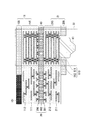
- FIG. 9 shows a configuration example of the imaging apparatus according to the present embodiment.
- the imaging apparatus according to the present embodiment may be an electronic device having an imaging function, and may be a digital video camera, an endoscope, or the like in addition to a digital camera.
- FIG. 9 includes a lens 81, an imaging unit 82, an image processing unit 83, a display unit 84, a drive control unit 85, a lens control unit 86, a camera control unit 87, and a camera operation unit 88. And have.
- a memory card 89 is also shown in FIG. 9, the memory card 89 may be configured to be detachable from the imaging apparatus. That is, the memory card 89 may not have a configuration unique to the imaging device.
- the lens 81 is a photographing lens for forming an optical image of a subject on the imaging surface of the imaging unit 82 constituting the solid-state imaging device.
- the imaging unit 82 converts the optical image of the subject formed by the lens 81 into a digital image signal by photoelectric conversion and outputs the digital image signal.
- the imaging unit 82 is a solid-state imaging device according to the first embodiment or the second embodiment.
- the image processing unit 83 performs various digital image processing on the image signal output from the imaging unit 82.
- the display unit 84 displays an image based on the image signal processed for display by the image processing unit 83.
- the display unit 84 can display a still image and can display a moving image (live view) display that displays an image of the imaged range in real time.
- the drive control unit 85 controls the operation of the imaging unit 82 based on an instruction from the camera control unit 87.
- the lens control unit 86 controls the aperture and the focal position of the lens 81 based on an instruction from the camera control unit 87.
- the camera control unit 87 controls the entire imaging apparatus.
- the operation of the camera control unit 87 is defined by a program stored in a ROM built in the imaging apparatus.
- the camera control unit 87 reads out this program and performs various controls according to the contents defined by the program.
- the camera operation unit 88 includes various members for operation for the user to perform various operation inputs to the imaging apparatus, and outputs a signal based on the result of the operation input to the camera control unit 87.
- Specific examples of the camera operation unit 88 include a power switch for turning on and off the imaging device, a release button for instructing still image shooting, and a still image shooting mode between the single shooting mode and the continuous shooting mode.
- a still image shooting mode switch for switching.
- the memory card 89 is a recording medium for storing the image signal processed for recording by the image processing unit 83.
- any of the solid-state imaging devices according to the first embodiment or the second embodiment is used for the imaging unit 82. For this reason, generation
- Each of the above embodiments can provide a semiconductor device, a solid-state imaging device, and an imaging device that can suppress the occurrence of cracks.
Landscapes
- Engineering & Computer Science (AREA)
- Multimedia (AREA)
- Signal Processing (AREA)
- Solid State Image Pick-Up Elements (AREA)
- Transforming Light Signals Into Electric Signals (AREA)
Priority Applications (1)
| Application Number | Priority Date | Filing Date | Title |
|---|---|---|---|
| US15/172,865 US20160284754A1 (en) | 2014-01-16 | 2016-06-03 | Semiconductor device, solid-state imaging device, and imaging apparatus |
Applications Claiming Priority (2)
| Application Number | Priority Date | Filing Date | Title |
|---|---|---|---|
| JP2014005596A JP2015135839A (ja) | 2014-01-16 | 2014-01-16 | 半導体装置、固体撮像装置、および撮像装置 |
| JP2014-005596 | 2014-01-16 |
Related Child Applications (1)
| Application Number | Title | Priority Date | Filing Date |
|---|---|---|---|
| US15/172,865 Continuation US20160284754A1 (en) | 2014-01-16 | 2016-06-03 | Semiconductor device, solid-state imaging device, and imaging apparatus |
Publications (1)
| Publication Number | Publication Date |
|---|---|
| WO2015108024A1 true WO2015108024A1 (ja) | 2015-07-23 |
Family
ID=53542913
Family Applications (1)
| Application Number | Title | Priority Date | Filing Date |
|---|---|---|---|
| PCT/JP2015/050617 Ceased WO2015108024A1 (ja) | 2014-01-16 | 2015-01-13 | 半導体装置、固体撮像装置、および撮像装置 |
Country Status (3)
| Country | Link |
|---|---|
| US (1) | US20160284754A1 (https=) |
| JP (1) | JP2015135839A (https=) |
| WO (1) | WO2015108024A1 (https=) |
Cited By (1)
| Publication number | Priority date | Publication date | Assignee | Title |
|---|---|---|---|---|
| CN107895689A (zh) * | 2016-10-04 | 2018-04-10 | 拉碧斯半导体株式会社 | 半导体装置 |
Families Citing this family (3)
| Publication number | Priority date | Publication date | Assignee | Title |
|---|---|---|---|---|
| JP5966048B1 (ja) * | 2015-04-09 | 2016-08-10 | 株式会社フジクラ | 撮像モジュール及び内視鏡 |
| KR102473664B1 (ko) * | 2016-01-19 | 2022-12-02 | 삼성전자주식회사 | Tsv 구조체를 가진 다중 적층 소자 |
| KR102725785B1 (ko) * | 2020-08-27 | 2024-11-04 | 삼성전자주식회사 | 반도체 패키지 및 반도체 패키지의 제조 방법 |
Citations (4)
| Publication number | Priority date | Publication date | Assignee | Title |
|---|---|---|---|---|
| JP2007103656A (ja) * | 2005-10-04 | 2007-04-19 | Denso Corp | 半導体装置およびその製造方法 |
| JP2011238951A (ja) * | 2011-07-08 | 2011-11-24 | Renesas Electronics Corp | 半導体装置およびその製造方法 |
| JP2012033894A (ja) * | 2010-06-30 | 2012-02-16 | Canon Inc | 固体撮像装置 |
| JP2013182941A (ja) * | 2012-02-29 | 2013-09-12 | Canon Inc | 固体撮像装置およびその製造方法 |
Family Cites Families (9)
| Publication number | Priority date | Publication date | Assignee | Title |
|---|---|---|---|---|
| JP3713418B2 (ja) * | 2000-05-30 | 2005-11-09 | 光正 小柳 | 3次元画像処理装置の製造方法 |
| JP4979154B2 (ja) * | 2000-06-07 | 2012-07-18 | ルネサスエレクトロニクス株式会社 | 半導体装置 |
| JP2002299595A (ja) * | 2001-04-03 | 2002-10-11 | Matsushita Electric Ind Co Ltd | 固体撮像装置およびその製造方法 |
| FR2910707B1 (fr) * | 2006-12-20 | 2009-06-12 | E2V Semiconductors Soc Par Act | Capteur d'image a haute densite d'integration |
| JP5583951B2 (ja) * | 2008-11-11 | 2014-09-03 | 株式会社半導体エネルギー研究所 | 半導体装置の作製方法 |
| TWI515885B (zh) * | 2009-12-25 | 2016-01-01 | 新力股份有限公司 | 半導體元件及其製造方法,及電子裝置 |
| JP5843475B2 (ja) * | 2010-06-30 | 2016-01-13 | キヤノン株式会社 | 固体撮像装置および固体撮像装置の製造方法 |
| JP5953087B2 (ja) * | 2012-01-17 | 2016-07-13 | オリンパス株式会社 | 固体撮像装置、撮像装置および固体撮像装置の製造方法 |
| JP6214132B2 (ja) * | 2012-02-29 | 2017-10-18 | キヤノン株式会社 | 光電変換装置、撮像システムおよび光電変換装置の製造方法 |
-
2014
- 2014-01-16 JP JP2014005596A patent/JP2015135839A/ja active Pending
-
2015
- 2015-01-13 WO PCT/JP2015/050617 patent/WO2015108024A1/ja not_active Ceased
-
2016
- 2016-06-03 US US15/172,865 patent/US20160284754A1/en not_active Abandoned
Patent Citations (4)
| Publication number | Priority date | Publication date | Assignee | Title |
|---|---|---|---|---|
| JP2007103656A (ja) * | 2005-10-04 | 2007-04-19 | Denso Corp | 半導体装置およびその製造方法 |
| JP2012033894A (ja) * | 2010-06-30 | 2012-02-16 | Canon Inc | 固体撮像装置 |
| JP2011238951A (ja) * | 2011-07-08 | 2011-11-24 | Renesas Electronics Corp | 半導体装置およびその製造方法 |
| JP2013182941A (ja) * | 2012-02-29 | 2013-09-12 | Canon Inc | 固体撮像装置およびその製造方法 |
Cited By (2)
| Publication number | Priority date | Publication date | Assignee | Title |
|---|---|---|---|---|
| CN107895689A (zh) * | 2016-10-04 | 2018-04-10 | 拉碧斯半导体株式会社 | 半导体装置 |
| CN107895689B (zh) * | 2016-10-04 | 2023-09-05 | 拉碧斯半导体株式会社 | 半导体装置 |
Also Published As
| Publication number | Publication date |
|---|---|
| JP2015135839A (ja) | 2015-07-27 |
| US20160284754A1 (en) | 2016-09-29 |
Similar Documents
| Publication | Publication Date | Title |
|---|---|---|
| CN108695349B (zh) | 具有层压层的半导体装置和设备 | |
| JP6177117B2 (ja) | 固体撮像装置、撮像装置、固体撮像装置の製造方法 | |
| US11000184B2 (en) | Image pickup module, fabrication method for image pickup module, and endoscope | |
| WO2012011326A1 (ja) | 撮像装置、内視鏡、および撮像装置の製造方法 | |
| WO2014122999A1 (ja) | 積層型固体撮像装置および撮像装置 | |
| WO2012063912A1 (ja) | 撮像装置 | |
| KR101902042B1 (ko) | 고체 촬상 소자 및 고체 촬상 소자의 실장 구조 | |
| WO2015108024A1 (ja) | 半導体装置、固体撮像装置、および撮像装置 | |
| WO2017077620A1 (ja) | 固体撮像装置 | |
| CN105074893A (zh) | 半导体基板、半导体装置、摄像元件及摄像装置 | |
| US20170263581A1 (en) | Electronic device, part mounting board, and electronic apparatus | |
| JP6600000B2 (ja) | 固体撮像装置および撮像装置 | |
| JP6990317B2 (ja) | 撮像ユニット及び撮像装置 | |
| JP6625615B2 (ja) | 撮像装置 | |
| US10199418B2 (en) | Semiconductor photodetection device | |
| WO2021090545A1 (ja) | 撮像素子および撮像装置 | |
| JP2021082620A (ja) | 撮像素子 | |
| JP5965984B2 (ja) | 撮像装置 | |
| US20250234665A1 (en) | Semiconductor device, manufacturing method therefor, and electronic apparatus | |
| JP2014096622A (ja) | カメラモジュール及び携帯端末 | |
| WO2016035184A1 (ja) | 固体撮像装置 | |
| JP6349089B2 (ja) | 半導体装置、及び撮像モジュール | |
| JP2025089934A (ja) | 光電変換装置および機器 | |
| WO2016103315A1 (ja) | 固体撮像装置および撮像装置 |
Legal Events
| Date | Code | Title | Description |
|---|---|---|---|
| 121 | Ep: the epo has been informed by wipo that ep was designated in this application |
Ref document number: 15737049 Country of ref document: EP Kind code of ref document: A1 |
|
| NENP | Non-entry into the national phase |
Ref country code: DE |
|
| 122 | Ep: pct application non-entry in european phase |
Ref document number: 15737049 Country of ref document: EP Kind code of ref document: A1 |