WO2015098728A1 - 積層型セラミック電子部品 - Google Patents
積層型セラミック電子部品 Download PDFInfo
- Publication number
- WO2015098728A1 WO2015098728A1 PCT/JP2014/083662 JP2014083662W WO2015098728A1 WO 2015098728 A1 WO2015098728 A1 WO 2015098728A1 JP 2014083662 W JP2014083662 W JP 2014083662W WO 2015098728 A1 WO2015098728 A1 WO 2015098728A1
- Authority
- WO
- WIPO (PCT)
- Prior art keywords
- dielectric ceramic
- internal electrode
- layer
- dielectric
- particles
- Prior art date
- Legal status (The legal status is an assumption and is not a legal conclusion. Google has not performed a legal analysis and makes no representation as to the accuracy of the status listed.)
- Ceased
Links
Images




Classifications
-
- H—ELECTRICITY
- H01—ELECTRIC ELEMENTS
- H01G—CAPACITORS; CAPACITORS, RECTIFIERS, DETECTORS, SWITCHING DEVICES, LIGHT-SENSITIVE OR TEMPERATURE-SENSITIVE DEVICES OF THE ELECTROLYTIC TYPE
- H01G4/00—Fixed capacitors; Processes of their manufacture
- H01G4/30—Stacked capacitors
-
- H—ELECTRICITY
- H01—ELECTRIC ELEMENTS
- H01G—CAPACITORS; CAPACITORS, RECTIFIERS, DETECTORS, SWITCHING DEVICES, LIGHT-SENSITIVE OR TEMPERATURE-SENSITIVE DEVICES OF THE ELECTROLYTIC TYPE
- H01G4/00—Fixed capacitors; Processes of their manufacture
- H01G4/002—Details
- H01G4/005—Electrodes
- H01G4/008—Selection of materials
- H01G4/0085—Fried electrodes
-
- H—ELECTRICITY
- H01—ELECTRIC ELEMENTS
- H01G—CAPACITORS; CAPACITORS, RECTIFIERS, DETECTORS, SWITCHING DEVICES, LIGHT-SENSITIVE OR TEMPERATURE-SENSITIVE DEVICES OF THE ELECTROLYTIC TYPE
- H01G4/00—Fixed capacitors; Processes of their manufacture
- H01G4/002—Details
- H01G4/005—Electrodes
- H01G4/012—Form of non-self-supporting electrodes
-
- H—ELECTRICITY
- H01—ELECTRIC ELEMENTS
- H01G—CAPACITORS; CAPACITORS, RECTIFIERS, DETECTORS, SWITCHING DEVICES, LIGHT-SENSITIVE OR TEMPERATURE-SENSITIVE DEVICES OF THE ELECTROLYTIC TYPE
- H01G4/00—Fixed capacitors; Processes of their manufacture
- H01G4/002—Details
- H01G4/018—Dielectrics
- H01G4/06—Solid dielectrics
- H01G4/08—Inorganic dielectrics
- H01G4/12—Ceramic dielectrics
-
- H—ELECTRICITY
- H01—ELECTRIC ELEMENTS
- H01G—CAPACITORS; CAPACITORS, RECTIFIERS, DETECTORS, SWITCHING DEVICES, LIGHT-SENSITIVE OR TEMPERATURE-SENSITIVE DEVICES OF THE ELECTROLYTIC TYPE
- H01G4/00—Fixed capacitors; Processes of their manufacture
- H01G4/002—Details
- H01G4/018—Dielectrics
- H01G4/06—Solid dielectrics
- H01G4/08—Inorganic dielectrics
- H01G4/12—Ceramic dielectrics
- H01G4/1209—Ceramic dielectrics characterised by the ceramic dielectric material
- H01G4/1218—Ceramic dielectrics characterised by the ceramic dielectric material based on titanium oxides or titanates
- H01G4/1227—Ceramic dielectrics characterised by the ceramic dielectric material based on titanium oxides or titanates based on alkaline earth titanates
-
- H—ELECTRICITY
- H01—ELECTRIC ELEMENTS
- H01G—CAPACITORS; CAPACITORS, RECTIFIERS, DETECTORS, SWITCHING DEVICES, LIGHT-SENSITIVE OR TEMPERATURE-SENSITIVE DEVICES OF THE ELECTROLYTIC TYPE
- H01G4/00—Fixed capacitors; Processes of their manufacture
- H01G4/002—Details
- H01G4/228—Terminals
- H01G4/248—Terminals the terminals embracing or surrounding the capacitive element, e.g. caps
Definitions
- the present invention relates to a multilayer ceramic electronic component.
- Equation 1 the capacitance of the multilayer ceramic capacitor is expressed by Equation 1. (Formula 1) C: electrostatic capacity, ⁇ r : relative permittivity, ⁇ 0 : vacuum permittivity, S: Internal electrode overlapping area, d: Dielectric ceramic layer thickness, n: Number of layers
- Equation 1 in order to increase the capacitance of the multilayer ceramic capacitor, considering that the overlapping area of the internal electrodes is almost constant, the intrinsic dielectric constant of the ceramic material is increased or the dielectric Adjustment is made by reducing the thickness of the body ceramic layer or increasing the number of laminated layers by reducing the thickness of the internal electrode layer.
- Patent Document 1 As a conventional technique for suppressing delamination of a multilayer ceramic capacitor or the like, for example, as shown in Patent Document 1, there is an electrode discontinuity portion due to dielectric ceramic particles grown on the internal electrode layer to the thickness of the internal electrode layer. There has been proposed a method of generating and having a function of an anchor such as a pillar connecting between the dielectric ceramic layers disposed above and below the internal electrode layer.
- Patent Document 2 acicular segregates are provided at the discontinuity of the internal electrode layer, and the acicular particles are arranged so as to penetrate the electrode discontinuity and bridge between the dielectric ceramic layers.
- a method of improving the adhesive strength between the internal electrode layer and the dielectric ceramic layer by increasing the contact area between the internal electrode layer and the dielectric ceramic layer has been proposed.
- Patent Document 2 can also be expected to have an effect of suppressing delamination, but in a multilayer ceramic capacitor having an internal electrode layer thinned to 0.5 ⁇ m or less, internal electrode particles are
- acicular segregated material mainly composed of Ba and Ti
- the adhesive strength between the acicular segregated material and the dielectric ceramic particles is not sufficient, and a crack occurs at the interface between the acicular segregated material and the dielectric ceramic particles.
- the present invention improves the adhesive strength between the internal electrode layer and the dielectric ceramic layer while suppressing the spheroidization of the conductive component of the internal electrode layer, suppresses the occurrence of cracks and delamination, and provides the bending strength. It is an object of the present invention to provide a multilayer ceramic electronic component having an internal electrode layer of 0.5 ⁇ m or less that improves the above.
- a multilayer ceramic electronic component is a laminate in which internal electrode layers and dielectric ceramic layers are alternately laminated, and the internal electrode layers have electrode breaks.
- a part of the electrode interruption part includes dielectric ceramic particles larger than the thickness of the dielectric ceramic layer in a cross section perpendicular to the stacking direction of the multilayer body, and the dielectric ceramic particles include the dielectric ceramic layer. It has the same kind of crystal structure as that of the dielectric ceramic particles contained therein, and is in contact with at least one of the internal electrode layers facing each other across the dielectric ceramic layer.
- the multilayer ceramic electronic component of the present invention has an electrode break portion, and the electrode break portion is composed of various ceramic particles, conductive component portions, and void portions where no ceramic particles exist.
- the ceramic particles are dielectric ceramic particles and do not stay in the internal electrode layer but are in contact with at least one of the adjacent internal electrode layers with the dielectric ceramic layer interposed therebetween.
- the dielectric ceramic layer is arranged so as to be bridged, the adhesion strength between the particles is increased, and the internal electrode layer can be firmly fixed with the dielectric ceramic particles at the electrode breaks.
- Adhesive strength is increased by the above structure, and the spheroidization of the conductive component generated during the firing process and the reoxidation process is suppressed, and the internal electrode layer is kept thin.
- the conductive component is spheroidized and energy that tends to swell in the stacking direction can be suppressed, cracks and delamination that occur at the interface between the internal electrode layer and the dielectric ceramic layer are effectively suppressed. can do.
- the dielectric ceramic particles having large grain growth are interposed in the internal electrode layer, so that the strength of the laminate is increased and the voids generated by the spheroidization of the conductive component in the internal electrode layer can be reduced. Therefore, the density of the laminate can be increased and the bending strength can be improved.
- the dielectric ceramic particles have the same kind of crystal structure as the dielectric ceramic particles forming the dielectric ceramic layer. As a result, the adhesion strength between the dielectric ceramic particles at the electrode break and the dielectric ceramic particles at the dielectric ceramic layer is improved, and the effects of cracks and delamination that occurs at the interface between the internal electrode layer and the dielectric ceramic layer are effective. Can be suppressed.
- the multilayer ceramic electronic component according to the present invention includes a dielectric ceramic particle in which a part of the dielectric ceramic particle is in contact with an end of the conductive component part formed in the electrode discontinuity part to form a dielectric ceramic layer. It is preferable that the grains grow larger.
- the electrode discontinuity part and the conductive component part end part are sandwiched between the dielectric ceramic layer and the dielectric ceramic particle of the electrode discontinuity part without gaps, so that the conductive component Spheroidization can be suppressed and delamination generated at the interface of the dielectric ceramic layer can be effectively suppressed.
- the dielectric ceramic particles constituting the electrode breakage portion have a large particle diameter, the dielectric constant is large, and since the gap portion is not interposed, the electrode breakage portion can also contribute to the capacitance.
- the ratio of the electrode discontinuity portion having the dielectric ceramic particles to the internal electrode layer is 5% or more and 15% when viewed in a cross section from a direction orthogonal to the stacking direction of the multilayer body. The following is preferable.
- the presence of the electrode discontinuity having the dielectric ceramic particles in the internal electrode layer within the above range effectively suppresses cracks and delamination without impairing the electrical characteristics of the multilayer ceramic electronic component. can do.
- the occurrence of cracks and delamination in a thin multilayered multilayer ceramic electronic component having a thin layer specifically, an internal electrode layer of 0.5 ⁇ m or less is suppressed, and the bending strength is improved. It becomes possible to do.
- FIG. 1 is a schematic cross-sectional view of a multilayer ceramic capacitor manufactured by a method for manufacturing a multilayer ceramic electronic component according to an embodiment of the present invention.
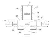
- FIG. 2 is a schematic view of a hot press firing furnace according to an embodiment of the present invention.
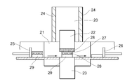
- FIG. 3 is a schematic view during firing in a hot press firing furnace according to an embodiment of the present invention.
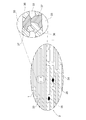
- FIG. 4 is a partial cross-sectional view of a multilayer ceramic capacitor for explaining the form of the internal structure of the multilayer ceramic electronic component according to the present invention.
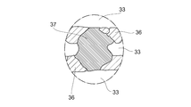
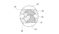
- FIG. 5 is an example of dielectric ceramic particles at the electrode discontinuity portion of the multilayer ceramic electronic component according to the present invention.
- FIG. 6 is an example of dielectric ceramic particles at the electrode breaks of the multilayer ceramic electronic component according to the present invention.
- FIG. 5 is an example of dielectric ceramic particles at the electrode discontinuity portion of the multilayer ceramic electronic component according to the present invention.
- FIG. 6 is an example of dielectric ceramic particles at the electrode breaks of the multilayer ceramic
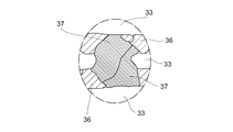
- FIG. 7 is an example of dielectric ceramic particles in the electrode breakage portion of the multilayer ceramic electronic component according to the present invention.
- FIG. 8 is an example of dielectric ceramic particles at the electrode discontinuity of the multilayer ceramic electronic component according to the present invention.
- FIG. 9 is an FE-SEM observation image (magnification 40,000 times) of the sample of Example 1.
- FIG. 10 is an FE-SEM observation image (magnification of 30,000 times) of the sample of Comparative Example 1.
- a multilayer ceramic capacitor will be described as an example.
- the same members are denoted by the same reference numerals, and redundant description is omitted.
- drawing is typical and the ratio of the dimension between members, the shape of a member, etc. may differ from an actual thing.
- a multilayer ceramic capacitor 10 As shown in FIG. 1, a multilayer ceramic capacitor 10 according to an embodiment of the present invention includes a multilayer body 3 having a configuration in which dielectric ceramic layers 1 and internal electrode layers 2 are alternately stacked. A pair of external electrodes 4 are formed on both ends of the laminate 3 so as to be electrically connected to the internal electrode layers 2 arranged alternately in the laminate.
- limiting in particular in the shape of the laminated body 3 Usually, it is set as a rectangular parallelepiped shape.
- composition of dielectric ceramic layer is not particularly limited, but it is mainly composed of ABO 3 (where A site contains at least Ba and B site represents a perovskite crystal containing at least Ti).
- Mg is 0.01 mol to 2.00 mol in terms of MgO with respect to 100 mol of ABO 3 , and an oxide of R (where R is Y, Dy, Ho, Yb, Lu, Gd, and Tb) 0.20 mol or more and 1.00 mol or less in terms of R 2 O 3 , SiO 2 in a range of 0.40 mol or more and 2.00 mol or less, and the oxide of Mn in excess of 0.00 mol in terms of MnO.
- the composition range of less than 0.50 mol and V oxide in the range of 0.01 mol to 0.50 mol in terms of V 2 O 5 is preferable.
- the organic component of the multilayer body 3 is contained by a known method such as production of dielectric ceramic paste, production of internal electrode paste, printing, lamination, and cutting. Things are made.
- a binder removal process, a firing process, and a reoxidation process are performed.
- the external electrode 4 is formed on the end face of the sintered laminated body 3, and the laminated ceramic capacitor 10 is completed.
- the dielectric ceramic layer paste in one embodiment of the present invention preferably uses a dielectric ceramic powder having an average particle size of 20 nm to 100 nm. By having an average particle diameter within this range, a dense dielectric green sheet can be produced, and in the firing step, grain growth of the dielectric ceramic powder can be promoted, and the structure according to the present invention is produced. It becomes possible.
- the internal electrode paste in one embodiment of the present invention is not particularly limited as the particle size of the conductive powder, but it is preferable to use one having an average particle size of 50 nm to 200 nm.
- the dielectric ceramic powder added as a co-material to delay the sintering behavior of the conductive powder is the same composition as that of the dielectric ceramic powder used in the dielectric ceramic paste and has an average particle size of about 100 nm to 200 nm. It is preferable to use ceramic powder. By having the average particle diameter of the co-material within this range, it becomes possible to produce the structure according to the present invention at the electrode discontinuity by reacting with the dielectric ceramic powder of the dielectric ceramic layer in the firing step. .
- the content of the common material is preferably 10% or more and 30% or less with respect to the conductive powder.
- the content of the common material is one of means for controlling the ratio of the electrode breaks.
- the raw material powder used as the co-material is preferably spherical and has poor crystallinity.
- the crystallinity of the barium titanate powder is 0.200 or more when the half-value width of the (111) plane is determined from the X-ray diffraction intensity. Is preferred. If the particle size is large and the crystallinity is good, it becomes difficult to react with the dielectric ceramic powder of the dielectric ceramic layer and grow large grains in the firing step.
- auxiliary material to the dielectric ceramic powder added to the internal electrode paste as a co-material so as to have the same composition as that of the dielectric ceramic layer, and the form of addition is not particularly limited.
- the method include baking addition, coating, and resinate.
- firing process In the firing step according to an embodiment of the present invention, since the particle size of the co-material of the internal electrode paste used in the present invention is large and the sintering behavior delay effect of the conductive powder cannot be expected, a special hot press sintering method is used. Used.
- the feature of the present invention lies in the structure, and any dielectric ceramic paste, internal electrode paste, and various firing methods may be used as long as the structure of the present invention can be produced. Examples include firing, hot isostatic pressing and batch furnace firing.
- the hot press firing apparatus is continuous high-speed hot press firing as shown in FIGS.
- the continuous high-speed hot press firing furnace in one embodiment of the present invention includes a pressure punch heating chamber 20, a pressure chamber 21, a punch 22, a stage 23, a heater 24, a pusher 25, and a receiver 26.
- the laminate sample 27 is placed on the high-strength plate 28, and the high-strength plate is provided on the ceramic base 29 and the bottom of the punch 23.
- the continuous high-speed hot press firing furnace has a punch 22 and a high-strength plate 28 that are heated from 1100 ° C. to 1300 ° C. in a pressure punch heating chamber 20. Sintering is performed by pressurizing and heating the laminate sample 27 placed on the ceramic table 29 and the high-strength plate 28. The laminated sample after sintering is taken out of the pressurizing chamber 21 by the receiver 26.
- Examples of the firing condition include a pressure amount condition of 1.0 MPa or more and 80 MPa or less at a rate of temperature increase of 7000 ° C./h or more and 100000 ° C./h or less.
- the hydrogen concentration is preferably greater than 0.1% and 4.0% or less in a coexistence atmosphere of nitrogen, hydrogen, and water vapor. If the hydrogen concentration is too high, the carbon remaining in the binder removal step remains in the firing step, and the reoxidation conditions shift to the high temperature side, which is not preferable. Conversely, when it becomes low, the conductive powder is oxidized, which is not preferable.
- high-strength plate materials that are strong against thermal shock such as tungsten carbide, silicon carbide, silicon nitride, etc. and have high bending strength are exemplified. It is preferable to use silicon carbide from the viewpoint of reactivity with the sample.
- Examples of the pressure punch described above include materials having high thermal conductivity such as silicon carbide and aluminum nitride. It is preferable to use silicon carbide from the viewpoint of heat resistance and thermal conductivity.
- materials having low thermal conductivity such as stabilized zirconia, alumina, silicon nitride, etc. are exemplified. From the viewpoint of thermal shock resistance and thermal conductivity, it is preferable to use stabilized zirconia or silicon nitride.
- the fired laminated body thus sintered is reoxidized.
- the reoxidation treatment may be performed while being pressurized in a hot press apparatus, or in another batch furnace or continuous furnace. In general, the reaction is performed in a coexistence atmosphere of nitrogen and water vapor in which the oxygen partial pressure is controlled to 10 ⁇ 8 atm to 10 ⁇ 4 atm.
- the holding temperature is preferably in the range of 800 ° C to 1100 ° C. If the holding temperature at the time of annealing is less than the above-described temperature range, the dielectric material may not be reoxidized sufficiently, so that the insulation resistance and life characteristics may deteriorate. In addition, if the above range is exceeded, it is difficult to obtain the structure of the present invention.
- the structure of the present invention can be obtained by passing the laminate produced using the dielectric ceramic paste and the internal electrode paste through the firing step and the reoxidation step.
- the form regarding the structure of this invention is demonstrated using FIG.
- FIG. 4 is a partially enlarged view of the internal structure of the schematic cross-sectional view of the multilayer ceramic capacitor of FIG.
- the internal electrode layer 2 when the cross section of the internal structure of the multilayer ceramic capacitor is enlarged, as shown in FIG. 4, it is composed of a dielectric ceramic layer 1 and an internal electrode layer 2, and the internal electrode layer 2 includes an electrode discontinuity portion and a conductive component portion 33. Consists of. Furthermore, the electrode interruption portion is composed of at least one of a ceramic portion 34 made of dielectric ceramic particles forming the dielectric ceramic layer 1 or ceramic particles analogous thereto, and a void portion 35 where no conductive component or ceramic particles are present.
- the ceramic portion 34 at the electrode interruption portion contains various particles such as dielectric ceramic particles 36, segregated oxide particles as additive subcomponents, ceramic particles changed from the main phase of the dielectric ceramic particles, and glass components.
- the dielectric ceramic particles are ceramic particles exhibiting ferroelectricity, and the ceramic particles mean all ceramic particles including those whose state is unknown.
- the dielectric ceramic particles 37 at the electrode discontinuity portion are dielectric materials whose main component is ABO 3 (wherein the A site represents at least Ba and the B site represents at least a perovskite crystal including Ti).
- the same kind as the main phase particles of the ceramic layer 1 is preferable.
- FIGS. 1 A part of the structure of the ceramic part of the electrode discontinuity according to one embodiment of the present invention is illustrated in FIGS.
- the dielectric ceramic particles 37 in contact with one of the dielectric ceramic layers 1 are mainly composed of ABO 3 (where the A site contains at least Ba and the B site represents a type crystal containing at least Ti). Because it is the same as the main phase particles, the adhesive strength of the dielectric ceramic layer with the dielectric ceramic particles is strong, and it suppresses spheroidization after the conductive component of the internal electrode layer is sintered in the firing and reoxidation processes. The occurrence of cracks and delamination can be suppressed.
- the strength of the laminate can be increased, and voids generated by the spheroidization of the conductive component in the internal electrode layer can be reduced.
- the density of the laminate is increased and the bending strength is improved.
- the conductive component portion in the internal electrode layer 2 adjacent to the dielectric ceramic layer 1 is not limited to the conductive component portion 33 in the internal electrode layer 2.
- the dielectric ceramic particles 37 in contact with at least one of the electrodes 33 are in contact with the electrode end portions of the conductive component portion 33 in the electrode interruption portion, and are further in contact with at least one of the opposing electrodes. Since it is sandwiched between the ceramic particles, delamination generated at the interface between the internal electrode layer and the dielectric ceramic layer can be effectively suppressed.
- the ratio of the electrode discontinuity portion having the dielectric ceramic particles 37 to the internal electrode layer 2 is 5% or more and 15% or less when the cross section is viewed from the direction orthogonal to the lamination direction of the laminate.
- the structure of the electrode break portion of the present invention is the same type as the dielectric ceramic layer main phase particles, unlike the voids, segregated particles, and specifically grown ceramic particles, which were the elements constituting the conventional electrode break portion. It has a crystal structure and is in contact with at least one of the opposing internal electrode layers with the dielectric ceramic layer sandwiched therebetween, so that the effect of suppressing cracks and delamination and the bending strength can be reduced by a small ratio of 5% to 15%. The effect of improvement is noticeable.
- the definition of the ratio of the electrode breakage portion according to the present invention in the internal electrode layer 2 is the ratio of the total length of the electrode breakage portion to the total length of the internal electrode layer 2 in the observation visual field.
- the center line is drawn horizontally with respect to the thickness of the internal electrode layer 2 and the length of the horizontal line and the length of the electrode breaks on the horizontal line are obtained.
- the shape of the dielectric ceramic particles present in a part of the electrode break portion is preferably an irregular shape.
- the particle shape is indefinite.
- the cross-sectional shape of the dielectric ceramic particles observed when the multi-layer ceramic electronic component is observed by cutting the cross-section perpendicular to the multi-layer surface is circular or square. It is not a simple shape with regularity such as a rectangle, but a shape having vertices and sides at irregular intervals, preferably a polygonal shape.
- the particle shape is irregular as described above, a large contact area between the particles can be obtained, the adhesion strength between the particles can be increased, the internal electrode layer can be firmly fixed at the electrode disconnection portion, and cracks can be generated. And delamination can be effectively suppressed.
- the occurrence of delamination and the bending strength are greatly reduced as compared with the conventional structure. To be improved.
- the present invention has been described above. However, the present invention is not limited to the above-described embodiments.
- the multilayer ceramic electronic component can be variously modified and applied without departing from the gist of the present invention.
- Mg is 0.1 mol
- Mn is 0.2 mol
- V is 0.1 mol
- Y is 0.8 mol
- Si is 1.3 mol
- Ba is 0.7 mol
- An auxiliary material having a composition of Ca of 0.5 mol was prepared.
- Mg is MgO
- Mn is MnCO 3
- V is V 2 O 5
- Y is Y 2 O 3
- Si, Ba, and Ca are SiO 2 , BaCO 3 , and CaCO 3 mixed, pulverized, and calcined. It was prepared as a fine powder.
- Ni powder (average particle diameter of 150 nm), barium calcium zirconate titanate dielectric ceramic powder having an average particle diameter of 150 nm, produced by changing the calcining temperature to 800 ° C. by the method described above, and a dielectric as an auxiliary material
- Various resinates and an organic vehicle were prepared so as to have the same composition as the ceramic powder.
- Ni powder, barium calcium zirconate titanate dielectric ceramic powder, various resinates of auxiliary materials, and organic vehicle were mixed with a homomixer, and then subjected to a dispersion treatment with an ultrasonic homogenizer for 30 minutes.
- the solvent was evaporated to some extent with an evaporator so that the concentration of inorganic solids in the paste was 40% by mass, and then kneaded with a three-roll mill to adjust the viscosity.
- the dielectric ceramic layer paste is prepared by mixing the dielectric ceramic powder and the organic vehicle with a homomixer, mixing with a dispersant, and grinding and mixing for 16 hours using 0.5 mm zirconia beads. did. *
- a dielectric green sheet was formed on a carrier film as a support by a slot die coating method.
- an internal electrode layer pattern was formed by screen printing on a dielectric green sheet using the internal electrode paste described above and dried.
- an outer layer green sheet in which only a dielectric green sheet was formed on a carrier film was prepared.
- the inner layer green sheet was laminated on the outer layer green sheet, and then the carrier film was peeled off.
- the inner layer green sheets were repeatedly laminated, and this operation was repeated up to a predetermined number of layers. And finally after laminating
- the obtained laminate was cut by applying a dicing saw.
- the cut and separated laminates were arranged on a high-strength plate at intervals of 0.1 mm, and the binder was removed together with the high-strength plate.
- silicon carbide was used as the high-strength plate.
- the binder removal conditions were a humidified nitrogen-hydrogen mixed gas having a hydrogen concentration of 4.0%, a holding temperature of 800 ° C., and a holding time of 12 hours.
- the temperature raising rate is not particularly limited, and the heating was performed until the residual carbon amount was 0.1% by mass or less.
- the obtained laminated chip on the high-strength plate was subjected to a baking temperature of 1160 ° C. and an applied pressure of 10 MPa at a rate of about 86400 ° C./h using the hot press baking apparatus shown in FIG. Sintering was performed under pressure conditions.
- the atmosphere during firing was a mixed gas of humidified nitrogen and hydrogen and an oxygen partial pressure of 10 ⁇ 11 atm.
- silicon carbide was used as the pressure punch, and silicon nitride was used as the ceramic table as the jig material of the hot press firing apparatus described above.
- the laminated body thus sintered was reoxidized.
- the reoxidation process was performed in a non-pressurized batch furnace in a coexistence atmosphere of nitrogen and water vapor controlled at 10 ⁇ 5 atm.
- the holding temperature was 1050 ° C.
- the obtained laminated body (sintered body chip) was subjected to end surface polishing by barrel polishing, and a terminal electrode was formed by baking a paste for Cu terminal electrode to form a multilayer ceramic capacitor having the structure of the present invention.
- the obtained multilayer ceramic capacitor was evaluated for particle shape, composition, ratio of ceramic part, number of delaminations, number of cracks, and bending strength constituting the ceramic part of the electrode discontinuity by the following evaluation method.
- the ceramic particles that are in contact with at least one of the adjacent internal electrode layers sandwiching the dielectric ceramic layer, not just within the internal electrode layer, are the same as the main phase particles of the dielectric ceramic layer. It confirmed that it was a dielectric ceramic particle.
- the average value of the internal electrode layer thickness in the observation field was 0.5 ⁇ m or less for all the evaluation samples.
- the cross section of the obtained multilayer ceramic capacitor was observed at 2500 times using a field emission scanning electron microscope (FE-SEM), and the ratio of electrode breaks was evaluated.
- the ratio of the electrode discontinuity shown in Tables 1 and 2 described later is larger than the thickness of the dielectric ceramic layer when a cross section perpendicular to the stacking direction of the stack is observed.
- the ratio of the electrode discontinuity in the internal electrode layer was the ratio of the length of the electrode discontinuity with respect to the length of the internal electrode layer in the visual field at the observation magnification described above.
- the length of the internal electrode layer and the electrode break is the sum of the horizontal lines drawn horizontally with respect to the thickness of the internal electrode layer, and the length of the electrode break is also the length of the electrode break on the horizontal line. It was calculated from the sum of Sa.
- the capacitance was measured under the conditions of 1 kHz and 1.0 Vrms using an LCR meter (4284A manufactured by HP), and a comparative evaluation was performed with an average value.
- FIG. 9 shows a cross-sectional observation FE-SEM image of the ceramic portion of the electrode breakage portion in Example 1.
- dielectric ceramic particles 37 larger than the thickness of the dielectric ceramic layer are present at the electrode breaks of the internal electrode layer, and the conductivity of the internal electrode layer is opposed to the dielectric ceramic layer. It was confirmed that it was in contact with at least one of the component parts 33.
- Example 2 and Example 3 were produced by the same process as in Example 1. However, in order to reduce the thickness of the internal electrode layer, the amount of internal electrode paste printed was reduced, and the ratio of electrode breaks, etc. Therefore, in Example 2, the firing holding temperature was 1130 ° C., the pressurization amount was 20 MPa, and the reoxidation holding temperature was 1000 ° C.
- Example 3 a sample was prepared with a firing holding temperature of 1140 ° C., a pressurization amount of 15 MPa, and a reoxidation treatment temperature of 1000 ° C. [Comparative example]
- Comparative Example 1 is a sample prepared by the method shown in Patent Document 1, but when using various materials and powders described in Patent Document 1, the internal electrode layer thickness does not become 0.5 ⁇ m or less.
- the dielectric ceramic material and the internal electrode paste shown below were used for manufacturing.
- barium titanate particles having an average particle diameter of 200 nm are used.
- Mg is 1.0 mol in terms of MgO and Y oxide is Y 2 O 3 with respect to 100 mol of barium titanate. Conversion was 0.60 mol, SiO 2 was 0.80 mol, Mn oxide was 0.30 mol in terms of MnO, and V oxide was 0.20 mol in terms of V 2 O 5 .
- a dielectric ceramic layer paste was prepared in the same manner as in the example.
- a paste was prepared in the same manner as in the example using Ni powder (average particle diameter 150 nm) and 20 nm barium titanate.
- the sample after the binder removal prepared by the above method was baked at a heating rate of 600 ° C./h and 1200 ° C., and the subsequent steps were the same as in the example.
- FIG. 10 shows a cross-sectional observation FE-SEM image of Comparative Example 1.
- the structure presented in Patent Document 1 was obtained, but the electrode discontinuity according to the present invention could not be confirmed.
- Comparative Example 2 is a sample prepared by the method shown in Patent Document 2, but when the internal electrode paste described in Patent Document 2 is used, the internal electrode layer thickness does not become 0.5 ⁇ m or less. It was produced using the dielectric ceramic material and internal electrode paste shown in 1.
- barium titanate particles having an average particle diameter of 200 nm are used.
- Mg is 1.9 mol in terms of MgO and Y oxide is Y 2 O 3 with respect to 100 mol of barium titanate. Conversion was 0.54 mol, BaSiO 3 was 0.50 mol, Cr oxide was 0.21 mol in terms of Cr 2 O 3 , and V oxide was 0.08 mol in terms of V 2 O 5 .
- a dielectric ceramic layer paste was prepared in the same manner as in the example.
- a paste was prepared in the same manner as in the example using Ni powder (average particle diameter 150 nm) and 20 nm barium titanate.
- the sample after the binder removal produced by the above method was baked at a heating rate of 600 ° C./h and 1200 ° C., and the subsequent steps were the same as in the example.
- Table 1 shows the evaluation results regarding Example 1, Example 2, Example 3, Comparative Example 1, and Comparative Example 2.
- the sample is not limited to the internal electrode layer obtained by the present invention, but has a dielectric ceramic particle in contact with at least one of the adjacent internal electrode layers with the dielectric ceramic layer interposed therebetween. Even when the internal electrode layer thickness is 0.5 ⁇ m or less, the number of cracks and delamination can be greatly improved compared to the conventional technology, and the bending strength is improved. did.
- Example 2 and Example 3 were not in the internal electrode layer, but were in contact with at least one of the adjacent internal electrode layers with the dielectric ceramic layer interposed therebetween, and the conductive component was not interposed in the gap.
- This is a sample in which there exist dielectric ceramic particles that are in contact with the end portions and grow larger than the dielectric ceramic particles forming the dielectric ceramic layer.
- the internal electrode layer was made very thin as 0.3 ⁇ m and the conductive component was easily spheroidized during the re-oxidation process, the number of delamination and cracks generated in 100 samples as shown in Table 1 Not observed.
- Example 2 and Example 3 the capacitance was improved by about 10%.
- the ratio of the electrode interruption part also contributed, but in Example 3, the ratio of the electrode interruption part was approximately the same, and an improvement in capacitance was confirmed. This is in contact with the end portion of the internal electrode formed in the electrode breakage portion and straddling the internal electrode layer in which the electrode breakage portion is formed and the electrode surface of the internal electrode layer facing each other through the dielectric ceramic layer. A large capacity can be obtained by arranging dielectric particles made of particles.
- Example 4 to Example 9 when viewed from the cross-sectional direction with respect to the stacking direction of the stacked body, the crystal structure is larger than the thickness of the dielectric ceramic layer and is the same kind as the dielectric ceramic particles forming the dielectric ceramic layer.
- the ratio of the electrode breaks is controlled. A sample was prepared.
- the amount of barium calcium zirconate titanate dielectric ceramic powder with a particle diameter of 150 nm and the conditions of the firing and reoxidation steps contained in the internal electrode paste are determined. Adjusted.
- the amount of internal electrode paste attached was adjusted as appropriate in accordance with the amount of dielectric ceramic powder added to the internal electrode paste so that the internal electrode thickness was 0.3 ⁇ m.
- Example 4 and Example 6 to Example 9 The firing holding temperature in Example 4 and Example 6 to Example 9 was 1140 ° C., and in Example 5, it was 1130 ° C.
- Example 4 and Example 5 the amount of pressurization was 20 MPa, in Example 6 and Example 7, the amount of pressurization was 15 MPa, and in Example 8 and Example 9, the amount of pressurization was 10 MPa.
- the holding temperature in the reoxidation process in Examples 4 to 9 was 950 ° C.
- Example 4 The evaluation results regarding Example 4 to Example 9 are shown in Table 2.
- the electrode discontinuity obtained by the present invention includes not only the internal electrode layer but also dielectric ceramic particles in contact with at least one of the adjacent internal electrode layers with the dielectric ceramic layer interposed therebetween. Then, when the ratio of the electrode discontinuity according to the present invention in the internal electrode layer is 5% or more and 15% or less, even if the number of cracks is 1000, the number of cracks and delamination It was confirmed that the frequency of occurrence was very small.
- the dielectric ceramic particles that do not stay in the internal electrode layer but are in contact with at least one of the adjacent internal electrode layers with the dielectric ceramic layer interposed therebetween provided with the electrode interruption part which has, it turns out that structural defects, such as a crack and delamination, were suppressed significantly and the bending strength also improved.
- the multilayer ceramic electronic component according to the present invention suppresses structural defects and guarantees high reliability even when the internal electrode layer is extremely thin. Therefore, it is very significant as a structure of a thin-layer multilayer electronic component. If the multilayer ceramic electronic component according to the present invention is, for example, a multilayer ceramic capacitor, a multilayer ceramic capacitor having a high capacity can be obtained. Therefore, the multilayer ceramic capacitor having this structure can be used for decoupling applications, waveform forming applications, filter applications, smoothing applications, and bypass applications of various communication equipment systems.
Landscapes
- Engineering & Computer Science (AREA)
- Power Engineering (AREA)
- Manufacturing & Machinery (AREA)
- Microelectronics & Electronic Packaging (AREA)
- Chemical & Material Sciences (AREA)
- Ceramic Engineering (AREA)
- Inorganic Chemistry (AREA)
- Materials Engineering (AREA)
- Ceramic Capacitors (AREA)
- Fixed Capacitors And Capacitor Manufacturing Machines (AREA)
Abstract
Description
(式1)

C:静電容量、εr:比誘電率、ε0:真空の誘電率、
S:内部電極重なり面積、d:誘電体セラミック層厚み、n:積層数
図1に示すように、本発明の一実施形態に係る積層セラミックコンデンサ10は、誘電体セラミック層1と内部電極層2とが交互に積層された構成の積層体3を有する。この積層体3の両端部には、積層体の内部で交互に配置された内部電極層2と各々導通する一対の外部電極4が形成してある。積層体3の形状に特に制限はないが、通常、直方体状とされる。また、その寸法にも特に制限はなく、用途に応じて適当な寸法とすればよい。
上述した誘電体セラミック層の組成は、特に限定される事はないが、ABO3(但し、Aサイトは、少なくともBaを含み、Bサイトは、少なくともTiを含むペロブスカイト型結晶を表す)を主成分とし、副原料として、ABO3100molに対して、MgがMgO換算で0.01mol以上2.00mol以下、Rの酸化物(ただし、Rは、Y、Dy、Ho、Yb、Lu、GdおよびTbから選ばれる少なくとも1つである)をR2O3換算で0.20mol以上1.00mol以下、SiO2を0.40mol以上2.00mol以下、Mnの酸化物をMnO換算で0.00molを超え、0.50mol未満、Vの酸化物をV2O5換算で0.01mol以上0.50mol以下で示す組成範囲のものが好ましい。
このような積層セラミックコンデンサ10を製造するに当たっては、誘電体セラミックペーストの作製、内部電極ペーストの作製、印刷、積層、切断といった、周知の方法により、積層体3の有機成分等を含んだ状態のものが作製される。次に有機成分等を炭化、燃焼させ、積層体3を焼結させる為に、脱バインダ工程、焼成工程、再酸化工程を経る。次いで焼結した積層体3の端面に外部電極4が形成され、積層セラミックコンデンサ10が完成する。
本発明の一実施形態における誘電体セラミック層用ペーストは、平均粒子径が20nmから100nmの誘電体セラミック粉末を用いることが好ましい。この範囲内に平均粒子径があることで、緻密な誘電体グリーンシートを作製できると共に、また焼成工程において、誘電体セラミック粉末の粒成長を促すことができ、本発明に係る構造体を作製することが可能になる。
本発明の一実施形態における内部電極ペーストは、導電性粉末の粒子径としては特に制限されないが、平均粒子径が50nmから200nmのものを用いることが好ましい。また共材として導電性粉末の焼結挙動を遅らせる為に添加される誘電体セラミック粉末は、誘電体セラミックペーストで用いる誘電体セラミック粉末と同組成で、平均粒子径で100nmから200nm程度の誘電体セラミック粉末を用いることが好ましい。この範囲内に共材の平均粒子径があることで、焼成工程において、誘電体セラミック層の誘電体セラミック粉末と反応し電極途切れ部に、本発明に係る構造体を作製することが可能になる。
本発明の一実施形態に係る焼成工程は、本発明で用いる内部電極ペーストの共材の粒子径が大きく、導電性粉末の焼結挙動遅延効果が望めないため、特殊なホットプレス焼結法が用いられる。しかし、本発明の特徴は構造体にあり、本発明の構造体が作製できる方法であれば、どのような誘電体セラミックペースト、内部電極ペースト、各種焼成方法を用いても良く、例えばローラーハースキルン焼成、熱間等方圧加圧焼成、バッチ炉焼成等が例示される。
BaCO3、CaCO3、TiO2、ZrO2を原料に用いてBa:Caが96:4、Ti:Zrが94:6の元素比になるようにそれぞれ調合し、700℃大気中で焼成した後にビーズミルで粉砕して、50nmのチタン酸ジルコン酸バリウムカルシウム粒子を得た。
Ni粉末(平均粒子径150nm)と、上記記載の方法で仮焼温度を800℃と変更して作製した、平均粒子径150nmのチタン酸ジルコン酸バリウムカルシウム系誘電体セラミック粉末と副原料として誘電体セラミック粉末と同一組成になるように各種レジネートと、有機ビヒクルとを準備した。
まず、誘電体セラミック層を構成する為の、誘電体グリーンシートを形成するために、チタン酸ジルコン酸バリウムカルシウム系誘電体セラミック粉末を含む誘電体セラミック層用ペーストを準備した。
得られた積層セラミックコンデンサは以下の評価方法により、電極途切れ部のセラミック部を構成する粒子形状、組成、セラミック部の割合、デラミネーション発生数、クラック発生数、抗折強度を評価した。
得られた積層セラミックコンデンサの断面を、電界放出形走査電子顕微鏡(FE-SEM)を用いて5000倍で観察し、電極途切れ部のセラミック部を特定した後、30000倍および40000倍で構成する粒子形状を評価した。
得られた積層セラミックコンデンサの断面のセラミック部のセラミック粒子をSTEMで観察し、エネルギー分散型X線分光(EDS)分析を行い、本発明に関係するセラミック粒子の組成を評価した。
得られた積層セラミックコンデンサの断面を、電界放出形走査電子顕微鏡(FE-SEM)を用いて2500倍で観察し、内部電極層厚みを評価した。
得られた積層セラミックコンデンサの断面を、電界放出形走査電子顕微鏡(FE-SEM)を用いて2500倍で観察し、電極途切れ部の割合を評価した。ここで後述する、表1、表2に示される電極途切れ部の割合とは、積層体の積層方向に対し、直交する切断面を観察したとき、誘電体セラミック層厚みよりも厚く、誘電体セラミック層を形成する誘電体セラミック粒子と同種の結晶構造を有し、誘電体セラミック層を挟んで対向する、内部電極層の少なくとも一方と接している誘電体セラミック粒子を含有した、電極途切れ部を意味する。
得られた積層セラミックコンデンサの六つの表面及び外部電極が観察できるよう断面を、レーザー顕微鏡(オリンパス製)を用いて20倍で観察し、クラックの発生数及びデラミネーションの発生数を評価した。
得られた積層セラミックコンデンサに対して、三点曲げ強度を測定した。測定条件は、支点間距離L=0.5mm、荷重速度=1mm/secとし、破壊時の荷重Pと次式から、積層型セラミックコンデンサの抗折強度Fを算出した。
F=(3×P×L)/(2×w×t2)
ただし、w:積層型セラミックコンデンサの幅、t:積層型セラミックコンデンサの厚みである。積層型セラミックコンデンサ100個について抗折強度Fを測定し、その平均値を求めた。
得られた積層セラミックコンデンサ10チップについて、LCRメーター(HP社製 4284A)を用いて1kHz、1.0Vrmsの条件で静電容量を測定し、平均値で比較評価を行った。
[比較例]


2・・・内部電極層
3・・・積層体
4・・・外部電極
10・・・積層セラミックコンデンサ
20・・・加圧パンチ加熱室
21・・・加圧室
22・・・パンチ
23・・・ステージ
24・・・ヒーター
25・・・プッシャー
26・・・受け
27・・・積層体試料
28・・・高強度プレート
29・・・セラミック台
33・・・導電性成分部
34・・・セラミック部
35・・・空隙部
36・・・誘電体セラミック粒子
37・・・誘電体セラミック層厚みよりも大きい誘電体セラミック粒子
Claims (3)
- 内部電極層と誘電体セラミック層とが交互に積層された積層体であって、
前記内部電極層は電極途切れ部を有し、
前記電極途切れ部の一部には、積層体の積層方向に直行する断面において、前記誘電体セラミック層厚みよりも大きい誘電体セラミック粒子を含み、
前記誘電体セラミック粒子は、誘電体セラミック層に含まれる誘電体セラミック粒子と同種の結晶構造を有し、前記誘電体セラミック層を挟んで対向する内部電極層の少なくとも一方と接することを特徴とする、積層型セラミック電子部品。 - 前記電極途切れ部の一部に存在する誘電体セラミック粒子は、前記電極途切れ部に形成された導電性成分部端部に接して、前記誘電体セラミック層を形成する前記誘電体セラミック粒子よりも大きく粒成長していることを特徴とする、請求項1に記載の積層型セラミック電子部品。
- 前記誘電体セラミック粒子を有する電極途切れ部は、前記積層体の積層方向に直行する断面において、内部電極層に占める割合が5%以上15%以下であることを特徴とする、請求項1乃至請求項3記載の積層型セラミック電子部品。
Priority Applications (3)
| Application Number | Priority Date | Filing Date | Title |
|---|---|---|---|
| CN201480071257.4A CN105849836B (zh) | 2013-12-25 | 2014-12-19 | 层叠型陶瓷电子部件 |
| US15/108,440 US9530566B2 (en) | 2013-12-25 | 2014-12-19 | Multilayer ceramic electronic component |
| JP2015554822A JP6314994B2 (ja) | 2013-12-25 | 2014-12-19 | 積層型セラミック電子部品 |
Applications Claiming Priority (2)
| Application Number | Priority Date | Filing Date | Title |
|---|---|---|---|
| JP2013-266350 | 2013-12-25 | ||
| JP2013266350 | 2013-12-25 |
Publications (1)
| Publication Number | Publication Date |
|---|---|
| WO2015098728A1 true WO2015098728A1 (ja) | 2015-07-02 |
Family
ID=53478586
Family Applications (1)
| Application Number | Title | Priority Date | Filing Date |
|---|---|---|---|
| PCT/JP2014/083662 Ceased WO2015098728A1 (ja) | 2013-12-25 | 2014-12-19 | 積層型セラミック電子部品 |
Country Status (4)
| Country | Link |
|---|---|
| US (1) | US9530566B2 (ja) |
| JP (1) | JP6314994B2 (ja) |
| CN (1) | CN105849836B (ja) |
| WO (1) | WO2015098728A1 (ja) |
Cited By (9)
| Publication number | Priority date | Publication date | Assignee | Title |
|---|---|---|---|---|
| JP2017175001A (ja) * | 2016-03-24 | 2017-09-28 | 京セラ株式会社 | 積層型電子部品 |
| JP2017228731A (ja) * | 2016-06-24 | 2017-12-28 | 京セラ株式会社 | 積層型電子部品 |
| US20180182549A1 (en) * | 2016-12-28 | 2018-06-28 | Tdk Corporation | Multilayer ceramic electronic device |
| JP2019145781A (ja) * | 2018-02-22 | 2019-08-29 | 太陽誘電株式会社 | 積層セラミック電子部品 |
| KR20190116144A (ko) * | 2019-07-29 | 2019-10-14 | 삼성전기주식회사 | 적층형 전자 부품 |
| JP2021141131A (ja) * | 2020-03-03 | 2021-09-16 | 太陽誘電株式会社 | セラミック電子部品の製造方法、および金属導電ペースト |
| JP2022182948A (ja) * | 2021-05-27 | 2022-12-08 | 太陽誘電株式会社 | セラミック電子部品およびセラミック電子部品の製造方法 |
| WO2024079966A1 (ja) * | 2022-10-13 | 2024-04-18 | 太陽誘電株式会社 | 積層セラミック電子部品 |
| JP2024101063A (ja) * | 2018-02-22 | 2024-07-26 | 太陽誘電株式会社 | 積層セラミック電子部品 |
Families Citing this family (10)
| Publication number | Priority date | Publication date | Assignee | Title |
|---|---|---|---|---|
| JP6753221B2 (ja) * | 2016-08-30 | 2020-09-09 | Tdk株式会社 | 誘電体組成物および積層電子部品 |
| JP6986360B2 (ja) * | 2017-04-05 | 2021-12-22 | 太陽誘電株式会社 | 積層セラミックコンデンサおよびその製造方法 |
| WO2019116761A1 (ja) * | 2017-12-11 | 2019-06-20 | 株式会社村田製作所 | リチウムイオン二次電池およびその製造方法 |
| JP2020167283A (ja) * | 2019-03-29 | 2020-10-08 | 株式会社村田製作所 | 積層セラミックコンデンサ |
| JP2020184555A (ja) * | 2019-04-26 | 2020-11-12 | 株式会社村田製作所 | 積層セラミックコンデンサ |
| JP7356831B2 (ja) * | 2019-07-17 | 2023-10-05 | 太陽誘電株式会社 | 積層セラミックコンデンサ及びその製造方法 |
| JP7821569B2 (ja) * | 2020-12-16 | 2026-02-27 | 太陽誘電株式会社 | 積層セラミックコンデンサおよび積層セラミックコンデンサの製造方法 |
| JP7585990B2 (ja) * | 2021-06-16 | 2024-11-19 | 株式会社村田製作所 | 積層セラミック電子部品 |
| JP7517260B2 (ja) * | 2021-06-16 | 2024-07-17 | 株式会社村田製作所 | 積層セラミック電子部品 |
| JPWO2023243159A1 (ja) * | 2022-06-16 | 2023-12-21 |
Citations (5)
| Publication number | Priority date | Publication date | Assignee | Title |
|---|---|---|---|---|
| JPH05283208A (ja) * | 1992-04-03 | 1993-10-29 | Murata Mfg Co Ltd | 積層型バリスタ |
| JP2003077761A (ja) * | 2001-09-05 | 2003-03-14 | Nec Tokin Ceramics Corp | 積層セラミックコンデンサ、及び積層セラミック部品 |
| JP2004342744A (ja) * | 2003-05-14 | 2004-12-02 | Murata Mfg Co Ltd | 積層セラミック電子部品 |
| JP2008198684A (ja) * | 2007-02-09 | 2008-08-28 | Matsushita Electric Ind Co Ltd | 積層セラミックコンデンサ |
| JP2008258190A (ja) * | 2007-03-30 | 2008-10-23 | Tdk Corp | 積層電子部品 |
Family Cites Families (7)
| Publication number | Priority date | Publication date | Assignee | Title |
|---|---|---|---|---|
| JPH10172855A (ja) * | 1996-12-05 | 1998-06-26 | Taiyo Yuden Co Ltd | 積層チップ部品とそれに用いる導電ペースト |
| US7158364B2 (en) * | 2005-03-01 | 2007-01-02 | Tdk Corporation | Multilayer ceramic capacitor and method of producing the same |
| JP5275918B2 (ja) * | 2009-06-24 | 2013-08-28 | Tdk株式会社 | 積層型セラミック電子部品 |
| JP2012129508A (ja) * | 2010-11-22 | 2012-07-05 | Tdk Corp | 積層型セラミック電子部品 |
| KR101197921B1 (ko) * | 2011-10-18 | 2012-11-05 | 삼성전기주식회사 | 적층 세라믹 전자 부품 |
| KR101823160B1 (ko) * | 2012-04-26 | 2018-01-29 | 삼성전기주식회사 | 적층 세라믹 전자부품 및 이의 제조방법 |
| US8971017B1 (en) * | 2014-10-30 | 2015-03-03 | Murata Manufacturing Co., Ltd. | Multilayer ceramic capacitor |
-
2014
- 2014-12-19 CN CN201480071257.4A patent/CN105849836B/zh active Active
- 2014-12-19 WO PCT/JP2014/083662 patent/WO2015098728A1/ja not_active Ceased
- 2014-12-19 US US15/108,440 patent/US9530566B2/en active Active
- 2014-12-19 JP JP2015554822A patent/JP6314994B2/ja active Active
Patent Citations (5)
| Publication number | Priority date | Publication date | Assignee | Title |
|---|---|---|---|---|
| JPH05283208A (ja) * | 1992-04-03 | 1993-10-29 | Murata Mfg Co Ltd | 積層型バリスタ |
| JP2003077761A (ja) * | 2001-09-05 | 2003-03-14 | Nec Tokin Ceramics Corp | 積層セラミックコンデンサ、及び積層セラミック部品 |
| JP2004342744A (ja) * | 2003-05-14 | 2004-12-02 | Murata Mfg Co Ltd | 積層セラミック電子部品 |
| JP2008198684A (ja) * | 2007-02-09 | 2008-08-28 | Matsushita Electric Ind Co Ltd | 積層セラミックコンデンサ |
| JP2008258190A (ja) * | 2007-03-30 | 2008-10-23 | Tdk Corp | 積層電子部品 |
Cited By (13)
| Publication number | Priority date | Publication date | Assignee | Title |
|---|---|---|---|---|
| JP2017175001A (ja) * | 2016-03-24 | 2017-09-28 | 京セラ株式会社 | 積層型電子部品 |
| JP2017228731A (ja) * | 2016-06-24 | 2017-12-28 | 京セラ株式会社 | 積層型電子部品 |
| US20180182549A1 (en) * | 2016-12-28 | 2018-06-28 | Tdk Corporation | Multilayer ceramic electronic device |
| JP2024101063A (ja) * | 2018-02-22 | 2024-07-26 | 太陽誘電株式会社 | 積層セラミック電子部品 |
| JP2019145781A (ja) * | 2018-02-22 | 2019-08-29 | 太陽誘電株式会社 | 積層セラミック電子部品 |
| KR20190116144A (ko) * | 2019-07-29 | 2019-10-14 | 삼성전기주식회사 | 적층형 전자 부품 |
| US12009150B2 (en) | 2019-07-29 | 2024-06-11 | Samsung Electro-Mechanics Co., Ltd. | Multilayer electronic component |
| KR102748942B1 (ko) * | 2019-07-29 | 2025-01-02 | 삼성전기주식회사 | 적층형 전자 부품 |
| JP2021141131A (ja) * | 2020-03-03 | 2021-09-16 | 太陽誘電株式会社 | セラミック電子部品の製造方法、および金属導電ペースト |
| JP7523922B2 (ja) | 2020-03-03 | 2024-07-29 | 太陽誘電株式会社 | セラミック電子部品の製造方法、および金属導電ペースト |
| JP2022182948A (ja) * | 2021-05-27 | 2022-12-08 | 太陽誘電株式会社 | セラミック電子部品およびセラミック電子部品の製造方法 |
| JP7780298B2 (ja) | 2021-05-27 | 2025-12-04 | 太陽誘電株式会社 | セラミック電子部品およびセラミック電子部品の製造方法 |
| WO2024079966A1 (ja) * | 2022-10-13 | 2024-04-18 | 太陽誘電株式会社 | 積層セラミック電子部品 |
Also Published As
| Publication number | Publication date |
|---|---|
| US9530566B2 (en) | 2016-12-27 |
| JP6314994B2 (ja) | 2018-04-25 |
| CN105849836B (zh) | 2018-08-31 |
| JPWO2015098728A1 (ja) | 2017-03-23 |
| CN105849836A (zh) | 2016-08-10 |
| US20160329151A1 (en) | 2016-11-10 |
Similar Documents
| Publication | Publication Date | Title |
|---|---|---|
| JP6314994B2 (ja) | 積層型セラミック電子部品 | |
| JP6443072B2 (ja) | 積層型セラミック電子部品 | |
| KR101464185B1 (ko) | 적층 세라믹 콘덴서 및 적층 세라믹 콘덴서의 제조방법 | |
| CN102483993B (zh) | 层叠陶瓷电容器的制造方法以及层叠陶瓷电容器 | |
| KR101697950B1 (ko) | 적층형 세라믹 전자 부품 | |
| KR101494851B1 (ko) | 적층 세라믹 콘덴서 및 적층 세라믹 콘덴서의 제조방법 | |
| JP2023060234A (ja) | 積層セラミックコンデンサ | |
| KR102520018B1 (ko) | 적층 세라믹 콘덴서 및 그 제조 방법 | |
| CN104779051A (zh) | 层叠型陶瓷电子部件 | |
| JP7131955B2 (ja) | 積層セラミックコンデンサおよびその製造方法 | |
| JP2009044017A (ja) | 積層セラミックコンデンサおよび積層セラミックコンデンサの製造方法 | |
| JP7357732B2 (ja) | セラミックコンデンサ | |
| JP2004292173A (ja) | 非還元性誘電体セラミックおよびその製造方法ならびに積層セラミックコンデンサ | |
| TWI441791B (zh) | 介電質陶瓷及積層陶瓷電容器 | |
| CN115403369A (zh) | 电介质组合物及层叠陶瓷电子部件 | |
| CN115403367B (zh) | 电介质组合物及层叠陶瓷电子部件 | |
| CN116580966A (zh) | 电介质材料和层叠陶瓷电子器件及其制造方法 | |
| JP4548118B2 (ja) | 誘電体磁器組成物、電子部品およびこれらの製造方法 | |
| CN116504438B (zh) | 电介质组合物及层叠陶瓷电子零件 | |
| JP4587924B2 (ja) | 積層セラミックコンデンサ | |
| US8395882B2 (en) | Dielectric ceramic and multilayer ceramic capacitor | |
| JP5229685B2 (ja) | 誘電体セラミック、及び積層セラミックコンデンサ | |
| JP2014232850A (ja) | 積層型電子部品 | |
| JP2011132056A (ja) | 積層セラミックコンデンサ | |
| JP2011129841A (ja) | 電子部品の製造方法 |
Legal Events
| Date | Code | Title | Description |
|---|---|---|---|
| 121 | Ep: the epo has been informed by wipo that ep was designated in this application |
Ref document number: 14874299 Country of ref document: EP Kind code of ref document: A1 |
|
| ENP | Entry into the national phase |
Ref document number: 2015554822 Country of ref document: JP Kind code of ref document: A |
|
| NENP | Non-entry into the national phase |
Ref country code: DE |
|
| WWE | Wipo information: entry into national phase |
Ref document number: 15108440 Country of ref document: US |
|
| 122 | Ep: pct application non-entry in european phase |
Ref document number: 14874299 Country of ref document: EP Kind code of ref document: A1 |