WO2015076369A1 - 静電チャック - Google Patents
静電チャック Download PDFInfo
- Publication number
- WO2015076369A1 WO2015076369A1 PCT/JP2014/080908 JP2014080908W WO2015076369A1 WO 2015076369 A1 WO2015076369 A1 WO 2015076369A1 JP 2014080908 W JP2014080908 W JP 2014080908W WO 2015076369 A1 WO2015076369 A1 WO 2015076369A1
- Authority
- WO
- WIPO (PCT)
- Prior art keywords
- electrostatic chuck
- top surface
- region
- conductive film
- protrusion
- Prior art date
- Legal status (The legal status is an assumption and is not a legal conclusion. Google has not performed a legal analysis and makes no representation as to the accuracy of the status listed.)
- Ceased
Links
Images




Classifications
-
- H—ELECTRICITY
- H10—SEMICONDUCTOR DEVICES; ELECTRIC SOLID-STATE DEVICES NOT OTHERWISE PROVIDED FOR
- H10P—GENERIC PROCESSES OR APPARATUS FOR THE MANUFACTURE OR TREATMENT OF DEVICES COVERED BY CLASS H10
- H10P72/00—Handling or holding of wafers, substrates or devices during manufacture or treatment thereof
- H10P72/70—Handling or holding of wafers, substrates or devices during manufacture or treatment thereof for supporting or gripping
- H10P72/72—Handling or holding of wafers, substrates or devices during manufacture or treatment thereof for supporting or gripping using electrostatic chucks
- H10P72/722—Details of electrostatic chucks
-
- H—ELECTRICITY
- H10—SEMICONDUCTOR DEVICES; ELECTRIC SOLID-STATE DEVICES NOT OTHERWISE PROVIDED FOR
- H10P—GENERIC PROCESSES OR APPARATUS FOR THE MANUFACTURE OR TREATMENT OF DEVICES COVERED BY CLASS H10
- H10P72/00—Handling or holding of wafers, substrates or devices during manufacture or treatment thereof
- H10P72/70—Handling or holding of wafers, substrates or devices during manufacture or treatment thereof for supporting or gripping
- H10P72/72—Handling or holding of wafers, substrates or devices during manufacture or treatment thereof for supporting or gripping using electrostatic chucks
-
- H—ELECTRICITY
- H10—SEMICONDUCTOR DEVICES; ELECTRIC SOLID-STATE DEVICES NOT OTHERWISE PROVIDED FOR
- H10P—GENERIC PROCESSES OR APPARATUS FOR THE MANUFACTURE OR TREATMENT OF DEVICES COVERED BY CLASS H10
- H10P72/00—Handling or holding of wafers, substrates or devices during manufacture or treatment thereof
- H10P72/70—Handling or holding of wafers, substrates or devices during manufacture or treatment thereof for supporting or gripping
- H10P72/76—Handling or holding of wafers, substrates or devices during manufacture or treatment thereof for supporting or gripping using mechanical means, e.g. clamps or pinches
- H10P72/7604—Handling or holding of wafers, substrates or devices during manufacture or treatment thereof for supporting or gripping using mechanical means, e.g. clamps or pinches the wafers being placed on a susceptor, stage or support
- H10P72/7614—Handling or holding of wafers, substrates or devices during manufacture or treatment thereof for supporting or gripping using mechanical means, e.g. clamps or pinches the wafers being placed on a susceptor, stage or support characterised by a plurality of individual support members, e.g. support posts or protrusions
Definitions
- the present invention relates to an electrostatic chuck that attracts an object when the object such as a wafer or a glass substrate is processed.
- various apparatuses such as an exposure apparatus or an inspection apparatus perform various processes on an object such as a semiconductor wafer or a glass substrate.
- Various apparatuses include an electrostatic chuck that attracts an object when the object is processed.
- Patent Document 1 describes an electrostatic chuck including a dielectric (base) having a suction surface (first surface) including a convex pin (protrusion surface portion) and a recess (bottom surface).
- the electrode for generating the Coulomb force and the bottom surface of the first surface for generating the Johnson Rahbek force are relatively far apart from the object. End up. That is, when the protrusion surface portion is provided for reducing the contamination of the object as described above, the attractive force of the electrostatic chuck with respect to the object tends to decrease.
- the substrate includes a base having a first surface including a bottom surface and a protruding surface portion protruding from the bottom surface, and the protruding surface portion includes a first top surface, the first top surface, And a step surface disposed between the bottom surface.
- the first top surface of the protrusion surface portion supports the object with a small contact area and suppresses contamination of the object by the particles.
- a relatively strong suction force can be generated in a region corresponding to the step surface disposed between the top surface and the bottom surface, so that the object can be suctioned relatively strongly.
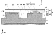
- FIG. 1 It is a perspective view which shows the electrostatic chuck by one Embodiment. It is the elements on larger scale of the cross section along the thickness direction which shows a mode that the target object was adsorbed
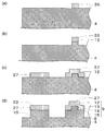
- or (d) are the elements on larger scale of the cross section along the thickness direction explaining the manufacturing method of the electrostatic chuck of FIG.
- or (c) are the elements on larger scale of the cross section along the thickness direction explaining the manufacturing method of the electrostatic chuck of FIG. It is the elements on larger scale of the cross section along the thickness direction which shows a mode that the target object was adsorbed
- the electrostatic chuck 1 shown in FIGS. 1 and 2 constitutes various apparatuses such as an exposure apparatus or an inspection apparatus, for example. These various devices are used, for example, in the manufacturing process of a semiconductor integrated circuit or a liquid crystal display device.
- the electrostatic chuck 1 attracts an object 2 such as a wafer or a glass substrate in various apparatuses.
- the object 2 attracted to the electrostatic chuck 1 is subjected to various processes in various apparatuses.
- the exposure apparatus includes an electrostatic chuck 1 and a light source. This exposure apparatus exposes the object 2 to form a wiring pattern by irradiating light onto the object 2 attracted to the electrostatic chuck 1 from a light source.
- the electrostatic chuck 1 electrostatically attracts the object 2 by Johnson-Rahbek force or Coulomb force. As shown in FIGS. 1 and 2, the electrostatic chuck 1 is disposed inside a base body 4 having a first surface 3, a conductive film 5 covering a part of the first surface 3, and the base body 4. The electrode 6 and the insertion hole 7 which penetrated the base
- the electrostatic chuck 1 includes a base 4 having a first surface 3 including a bottom surface 8 and a protruding surface portion 9 protruding from the bottom surface 8, and the protruding surface portion 9 includes a first top surface 12, a first top surface 12, And a step surface 14 disposed between the bottom surface 8 and the bottom surface 8.
- the first surface 3 further includes a peripheral convex surface portion 10 protruding from the bottom surface 8 together with the bottom surface 8 and the plurality of protruding surface portions 9.
- the base 4 has a flat plate portion, a plurality of protrusions provided on the main surface of the flat plate portion, and a convex portion provided on the main surface of the flat plate portion and arranged so as to surround the plurality of protrusions.
- the protrusion has a two-step shape in the cross section along the thickness direction, the surface of the protrusion is the protrusion surface portion 9, the top surface of the upper step is the first top surface 12, and the upper step The top surface of the lower step that surrounds is the step surface 14.
- the convex portion has a rectangular shape in a cross section along the thickness direction, the surface of the convex portion is the peripheral convex surface portion 10, and the top surface is the second top surface 23.
- the part in which the protrusion and convex part are not provided in the main surface of a flat plate part is a bottom face.
- the convex portion is continuous along the peripheral line of the bottom surface 8.
- the substrate 4 is, for example, an aluminum oxide sintered body, an aluminum nitride sintered body, a silicon nitride sintered body, a cordierite sintered body, or a silicon carbide sintered body (SiC-based or Si-SiC-based). Made of ceramics. Among these, it is desirable that the substrate 4 is made of an aluminum oxide sintered body or an aluminum nitride sintered body.
- the substrate 4 has a plate shape such as a disk shape or a square plate shape, and the substrate 4 of the present embodiment has a disk shape.
- the thickness of the base 4 is, for example, 1 mm or more and 50 mm or less. Moreover, the width
- a space 11 is formed between the first surface 3 of the electrostatic chuck 1 and the object 2.
- a fluid such as a gas for adjusting the temperature of the object 2 is supplied to the space 11.
- This fluid may be supplied to the space 11 from a flow path (not shown) disposed in the base 4 and opened in the first surface 3.
- the bottom surface 8 is, for example, a flat surface.
- the protrusion surface portion 9 has a first top surface 12 and a step surface 14 disposed between the first top surface 12 and the bottom surface 8.
- the first top surface 2 of the projection surface portion 9 functions as a support surface that supports the object 2. More specifically, the protrusion surface portion 9 includes the first top surface 12, the first side surface 13 connected to the outer periphery of the first top surface 12, and the first side surface 13 opposite to the first top surface 12.
- a step surface 14 connected to the end portion and a second side surface 15 connected to the outer periphery of the step surface 14 are provided.
- the peripheral convex surface portion 10 has a frame shape when viewed in plan, for example, a polygonal shape such as a circular shape or a quadrangular shape. Note that a part of the peripheral convex surface portion 10 may be wavy in a plan view, or may partially protrude toward the inside of the frame-shaped convex portion.
- the conductive film 5 covers at least a part of the first top surface 12 of the projection surface portion 9 and partially covers the step surface 14. Thereby, drop-off of particles from a part of the first surface 3 is reduced.
- the conductive film 5 may not cover the step surface 14.
- the conductive film 5 is grounded, for example, to release the charge in the object 2 in contact with the conductive film 5 to the outside.
- the conductive film 5 is grounded by being electrically connected to the ground terminal of various devices.
- the conductive film 5 is made of a ceramic film, a metal film, or a resin film.
- the ceramic film is made of, for example, a conductive ceramic material or a ceramic material with added conductivity.
- a ceramic film is made of, for example, a ceramic material such as silicon oxide, silicon nitride, titanium nitride, titanium carbide, alumina, or DLC (Diamond-like Carbon).
- the metal film is made of a metal material such as aluminum, chromium, or gold.
- the resin film is made of a conductive resin material or a resin material with conductivity added.
- Such a resin film is made of, for example, a resin material such as a polythiophene resin or a polyacetylene resin.
- a Si-based material such as silicon oxide or silicon nitride
- a Ti-based material such as titanium nitride or titanium carbide
- a C-based material such as DLC
- the thickness of the conductive film 5 is, for example, not less than 0.01 ⁇ m and not more than 10 ⁇ m.
- the electrode 6 has a function of generating an attracting force on the electrostatic chuck 1 when a voltage is applied thereto.
- the electrode 6 is made of a metal such as tungsten, tungsten carbide, molybdenum, or platinum.
- the electrode 6 is disposed so as to uniformly spread over a region corresponding to the entire surface of the first surface 3 excluding a part along the peripheral line in plan perspective. Note that various shapes of the electrode 6 can be selected according to the shape of the target object 2, a desired adsorption force distribution state, and the like.
- the electrode 6 may be provided with a slit in a part of the region in a plan view, or may be provided partially in a range corresponding to a part of the region of the first surface 3. Even in such a case, the electrode 6 is disposed at a position corresponding to at least the bottom surface 8 and the step surface 14 (a position overlapping in plan view).
- the adsorption of the object 2 by the electrostatic chuck 1 described above is performed as follows, for example. First, after the top surface of the lift pin inserted through the insertion hole 7 is moved above the first surface 3, the object 2 is placed on the lift pin. Next, the top surface of the lift pin is moved below the first surface 3 to bring the object 2 into contact with the first top surface 12 of the protrusion surface portion 9. Next, by applying a voltage to the electrode 6, an attracting force is generated in the electrostatic chuck 1 to attract the object 2 to the first surface 3. As described above, the object 2 can be fixed by the electrostatic chuck 1.
- the protrusion surface portion 9 has the first top surface 12, and the object 2 comes into contact with the first top surface 12, so that the electrostatic chuck 1 and the object 2 are in contact with each other.
- the area can be reduced. For this reason, it is possible to reduce contamination of the object 2 by particles generated from the substrate 4 or particles adhering to the substrate 4.
- the flatness of the target object 2 in the adsorbed state can be increased, and the processing accuracy of the target object 2 can be increased.
- the protrusion surface portion 9 has a first top surface 12 and a step surface 14 disposed between the first top surface 12 and the bottom surface 8.
- a relatively strong adsorption force is generated between the stepped surface 14 and the object 2.
- the step surface 14 constitutes a part of the projection surface portion 9 protruding from the bottom surface 8, and the distance between the object 2 and the step surface 14 is larger than the distance between the object 2 and the bottom surface 8. small.
- An adsorption force due to the potential difference between the electrode 6 and the object 2 acts between the object 2 and the step surface 14 and between the object part 2 and the bottom surface 8. Adsorbed to be attracted to the surface 14.
- the region corresponding to the step surface 14 has a larger attraction force. This is because the step surface 14 is closer to the object 2 than the bottom surface 8, and a relatively strong adsorption force acts between the step surface 14 and the object 2.
- a relatively strong adsorption force can be realized. Thereby, the position shift of the target object 2 attracted to the electrostatic chuck 1 can be suppressed, and the processing accuracy of the target object 2 can be increased.
- the attracting force at the step surface 14 located in the vicinity of the first top surface 12 in contact with the object 2 is relatively high, the voltage applied to the electrode 6 is maintained while maintaining the attracting force of the electrostatic chuck 1. It can be made relatively small. Thereby, the leakage current to the object 2 can be reduced, and the heat generation of the object 2 and the base 4 due to the leakage current can be suppressed. Therefore, the thermal expansion of the target object 2 resulting from this heat can be suppressed, and the processing accuracy of the target object 2 can be increased.
- the adsorption force in the region corresponding to the bottom surface 8 located relatively far from the first top surface 12 can be made relatively small. I can leave.
- the suction force at the bottom surface 8 located relatively far from the first top surface 12 is relatively strong, deformation of the target portion 2 such as bending of the object 2 due to the suction force is likely to occur.
- the projection surface portion 9 has the step surface 14 between the first top surface 12 and the bottom surface 8, the suction force in the region corresponding to the step surface 14 is relatively increased.
- the electrostatic chuck 1 can suppress the deformation of the object 2 due to the attracting force and can increase the flatness of the object 2.
- the object 2 is relatively strongly adsorbed in the region corresponding to the stepped surface 14, the object 2 is pressed relatively strongly against the first top surface 12, and the frictional force between the first top surface 12 and the object 2 is large. .
- the electrostatic chuck 1 can satisfactorily suppress the displacement of the object 2 attracted to the electrostatic chuck 1 by this frictional force.
- a fluid such as a gas for adjusting the temperature of the object 2 is supplied to the space 11.
- the temperature of the object 2 adsorbed can be adjusted by exchanging heat with this gas or the like.
- this gas flow for example, fine particles move in the space 11 on the gas.
- the projection surface portion 9 has a step surface 14, and in the region corresponding to the step surface 14, the gap between the step surface 14 and the object 2 is narrow, so that it is difficult for gas to enter.
- the region corresponding to the stepped surface 14 can function as a static pressure seal, and particles can be prevented from approaching the first top surface 12.
- the step surface 14 is disposed closer to the object 2 than the bottom surface 8, so that the object is radiated from the step surface 14. The temperature of 2 can be adjusted.
- the step surface 14 is disposed so as to surround the first top surface 12 in a plan view, and particles approaching the first top surface 12 can be more reliably suppressed.
- the protrusion surface portion 9 includes a first portion 16 having a first top surface 12 and a first side surface 13 on the surface, and a second portion 17 having a step surface 14 and a second side surface 15.
- the protruding portion having the protruding surface portion 9 as a surface is a two-step protrusion.
- the protruding portion may have three or more protruding shapes, and the protruding surface portion 9 may have a plurality of stepped surfaces 14.
- the inclination angle of the step surface 14 with respect to the first top surface 12 is smaller than the inclination angle of the first side surface 13 with respect to the first top surface 12.
- the step surface 14 is preferably substantially parallel to the first top surface 12.
- the inclination angle of the step surface 14 with respect to the first top surface 12 is, for example, not less than 0 ° and not more than 3 °.
- the electrostatic chuck 1 includes a conductive film 5 that covers at least a part of the first top surface 12 and partially covers the step surface 14.
- “Partially covering the step surface 14” means a state in which a part or a plurality of portions of the step surface 14 are exposed without being covered with the conductive film 5, as shown in FIGS. 2 and 3. . That is, the step surface 14 has an exposed portion 18 that is exposed without being covered with the conductive film 5. Since the conductive film 5 covers at least a part of the first top surface 12 in this way, by grounding the conductive film 5, at least a part of the region of the first top surface 12 is made to have a potential of the conductive film 5. (That is, ground potential).
- the portion corresponding to the conductive film 5 can be configured not to generate an adsorption force for adsorbing the object 2.
- the conductive film 5 covers at least a part of the first top surface 12, it is possible to reduce the falling off of particles on the first top surface 12. Therefore, contamination of the target object 2 by particles can be reduced and the flatness of the target object 2 can be increased.
- the conductive film 5 since the adsorption force can be suppressed only by having the conductive film 5, the conductive film 5 does not necessarily need to be grounded. Even in this case, it is preferable that the conductive film 5 is grounded after the adsorption so that the charge reaching the conductive film 5 can be quickly released to the outside through the conductive film 5.
- a connection switching unit such as a switch may be provided between the conductive film 5 and the ground potential. In the case where charges are accumulated in the object 2 at the time of adsorption, the charges accumulated in the object 2 can be quickly released to the outside by grounding the conductive film 5. Thereby, the time for detaching the object 2 from the electrostatic chuck 1 can be shortened, and the processing speed of the object 2 by various apparatuses can be increased.
- a voltage for adsorbing the object 2 is applied to the electrode 6 while the conductive film 5 is grounded. At this time, since the conductive film 5 is at the ground potential, no force that attracts the object 2 is generated in a region corresponding to the conductive film 5.
- the stepped surface 14 has an exposed portion 18 exposed from the conductive film 5. Since the region corresponding to the exposed portion 18 is exposed from the conductive film 5, an attractive force is generated. Since the exposed portion 18 of the stepped surface 14 is closer to the object 2 than the bottom surface 8, the suction force in the region corresponding to the exposed portion 18 is relatively high.
- the electrostatic chuck 1 As described above, in the electrostatic chuck 1, the attracting force on the first top surface 12 that is in contact with the object 2 is suppressed by the conductive film 5, and the first top surface 12 is damaged by the object 2 and the damage is caused. The generation of broken particles is suppressed.
- the exposed portion 18 is disposed on the stepped surface 14 by partially covering or not covering the stepped surface 14, thereby realizing a relatively strong adsorption force in the vicinity of the first top surface 12.
- the conductive film 5 covers the entire first top surface 12, but the conductive film 5 may cover only a part of the first top surface 12.
- the first side surface 13 surrounds the first top surface 12 in the circumferential direction D1.
- the conductive film 5 has a first region 19 that covers at least a part of the first top surface 12, and a second region 20 that covers the first side surface 13 in the circumferential direction D ⁇ b> 1 and is connected to the first region 19. And have.
- the first region 19 can be electrically connected to the ground via the second region 20.
- the second region 20 covers the first side surface 13 in the circumferential direction D1 and is connected to the first region 19, the connection strength between the first region 19 and the second region 20 is increased. Can do. Thereby, disconnection between the first region 19 and the second region 20 can be reduced.
- region 20 has covered the 1st side surface 13 over the circumferential direction D1, drop-off
- the conductive film 5 further includes a third region 21 that covers a region near the first side surface 13 in the step surface 14 over the circumferential direction D1 and is connected to the second region 20.
- the second region 20 can be electrically connected to the ground via the third region 21.
- the third region 21 covers the region near the first side surface 13 in the step surface 14 over the circumferential direction D1 and is connected to the second region 20, the second region 20 and the third region 21 are connected. Connection strength can be increased. Thereby, disconnection between the second region 20 and the third region 21 can be reduced.
- the conductive film 5 further includes a linear fourth region 22 that covers a part of the region other than the region near the first side surface 13 on the stepped surface 14 and is connected to the third region 21.
- the third region 21 can be electrically connected to the ground via the fourth region 22.
- step difference surface 14 can be enlarged by making a 4th area
- a plurality of protrusion surface portions 9 protrude from the bottom surface 8, and the fourth region 22 of each protrusion surface portion 9 is connected to the fourth region 22 of one or more other protrusion surface portions 9. Yes.
- the fourth regions 22 of each of the plurality of protrusion surface portions 9 are electrically connected via the wiring 41 formed on the bottom surface 8.
- positioned at the some projection surface part 9 can be electrically connected by a small wiring area.
- the conductive films 5 of the plurality of projection surface portions 9 are all electrically connected, and one location electrically connected to the conductive film 5 is grounded, so that the plurality of projection surface portions 9 are grounded. All of the conductive films 5 can be grounded simultaneously.
- the distance between the first top surface 12 and the step surface 14 in the height direction (Z direction) of the projection surface portion 9 (the height of the first portion 16) is 0.05 ⁇ m or more and 10 ⁇ m or less.
- this distance is 10 ⁇ m or less, the distance between the step surface 14 and the object 2 can be made sufficiently small, and the suction force on the step surface 14 can be increased.
- this distance is possible to suppress the distance between the step surface 14 and the first top surface 12 from being too close, and to generate an adsorption force on the step surface 14.
- the first top surface 12 and the step surface 14 of the projection surface portion 9 The distance is more preferably 1 ⁇ m or more and 3 ⁇ m or less.
- the step surface 14 can function as a static pressure seal, and a decrease in flatness of the object 2 due to particles dropped from the step surface 14 close to the object 2 is suppressed. it can. Further, when the step surface 14 functions as a static pressure seal, it becomes difficult for the temperature adjusting gas to enter, but since the distance between the step surface 14 and the object 2 becomes small, the temperature of the object 2 can be adjusted favorably by radiant heat. can do.
- the height of the first top surface 12 in the projection surface portion 9 (the distance between the first top surface 12 and the bottom surface 8 in the height direction of the projection) is, for example, 3 ⁇ m or more and 50 ⁇ m or less. Since the height of the first top surface 12 is 3 ⁇ m or more, the space 11 between the object 2 and the bottom surface 8 can be enlarged, and the temperature of the object 2 can be adjusted favorably by the gas disposed in the space 11. it can. Further, the height of the step surface 14 in the protrusion surface portion 9 (the distance between the step surface 14 and the bottom surface 8 in the height direction of the protrusion) is, for example, not less than 1 ⁇ m and not more than 49 ⁇ m.
- variety (diameter) of the 1st top surface 12 is 0.03 mm or more and 10 mm or less, for example.
- the width of the step surface 14 (the distance between the inner periphery and the outer periphery of the step surface 14) is, for example, not less than 0.01 mm and not more than 9.97 mm.
- the width of the third region 21 in the conductive film 5 (the distance between the inner periphery and the outer periphery in the third region 21) is, for example, 0.001 mm or more and 8.00 mm or less.
- the width of the exposed portion 18 on the step surface 14 (the distance between the inner periphery and the outer periphery of the exposed portion 18) is, for example, 0.001 mm or more and 9.97 mm or less.
- the first surface 3 has a peripheral convex surface portion 10 that protrudes from the bottom surface 8 and is provided so as to surround a plurality of protrusions. By having the peripheral convex surface portion 10, external leakage of gas in the space 11 can be suppressed.
- the peripheral convex surface portion 10 has a second top surface 23, and the height of the second top surface 23 from the bottom surface 8 is smaller than the height of the first top surface 12 from the bottom surface 8. By making the difference in height between the first top surface 12 and the second top surface 23 minute, a minute gap 24 that is a space is formed between the object 2 and the second top surface 23.
- the minute gap 24 functions as a static pressure seal because the amount of movement of fluid such as air is extremely small because the gap is minute, and gas from the space 11 between the object 2 and the first surface 3 etc. Can be suppressed. Further, since the minute gap 24 causes a gap between the object 2 and the second top surface 23 and contact is suppressed, the inclination of the object 2 due to this contact can be suppressed. Therefore, since the flatness of the target object 2 can be increased, the processing accuracy of the target object 2 can be increased.
- the entire width of the peripheral convex surface portion 10 is such that the distance between the outer periphery and the inner periphery is 0.01 mm or more and 5 mm or less, for example.
- the width of the peripheral convex surface portion 10 is larger than the width of the protrusion surface portion 9.
- the entire width of the peripheral convex surface portion 10 may be the same as or different from the entire width of the protrusion surface portion 9.
- the peripheral convex surface portion 10 has a second top surface 23 whose height from the bottom surface 8 is the same as the step surface 14 of the projection surface portion 9. That is, the distance between the second top surface 23 and the bottom surface 8 in the height direction of the projection surface portion 9 is the same as the distance between the step surface 14 and the bottom surface 8 in the height direction of the projection surface portion 9. Moreover, since the height of the 2nd top surface 23 is the same as the height of the level
- the thickness of the minute gap 24 is, for example, not less than 0.5 ⁇ m and not more than 20 ⁇ m.
- the thickness of the minute gap 24 is 0.5 ⁇ m or more, the contact between the object 2 and the second top surface 23 can be further suppressed. Further, when the thickness of the minute gap 24 is 20 ⁇ m or less, outflow of gas or the like from the space 11 between the object 2 and the first surface 3 can be suppressed.
- the thickness of the minute gap 24 is desirably 1 ⁇ m or more and 3 ⁇ m or less.
- the electrostatic chuck 1 has a second conductive film 25 that covers at least a part of the second top surface 23.
- the second conductive film 25 is electrically connected to the conductive film 5.
- the second top surface 23 covered with the second conductive film 25 has the same force as the first top surface 12 covered with the conductive film 5 to attract the object 2. Does not emit.
- the force for adsorbing the object 2 can be suppressed as in the first top surface 12 covered with the conductive film 5. Therefore, the deformation of the object 2 due to the suction force of the second top surface 23 can be reduced, and the flatness of the object 2 can be increased. Moreover, the drop-off of particles on the second top surface 23 can be reduced.
- the conductive film 25 covers the entire second top surface 23. Note that the second conductive film 25 and the conductive film 5 may not be electrically connected. Also in this case, if the second conductive film 25 and the conductive film 5 are grounded, the second conductive film 25 and the conductive film 5 have the same effects as in the above-described embodiment.
- the second conductive film 25 covers the side surface of the peripheral convex surface portion 10 and the region near the peripheral convex surface portion 10 on the bottom surface 8. Further, since the thickness of the second conductive film 25 and the thickness of the first region 20 of the conductive film 5 are the same, the thickness of the minute gap 24 is the distance between the first top surface 12 and the second top surface 23. .
- the substrate 4 is prepared. Specifically, for example, the following is performed.
- the ceramic powder First, pure water and an organic binder are added to the ceramic powder, and then wet mixed with a ball mill to prepare a slurry. Next, the slurry is granulated by spray drying to produce ceramic particles. Next, the ceramic particles are molded using various molding methods to produce a molded body. At this time, an electrode paste is formed inside the molded body.
- a molded body can be produced, for example, by applying an electrode paste to a tape produced by tape-molding ceramic particles and then laminating another tape on the electrode paste.
- the formed body is formed into a desired shape by cutting the formed body. Next, this molded body is fired at, for example, 1000 ° C. or higher and 2300 ° C. or lower to form a ceramic sintered body. At this time, the electrode 6 is formed by co-firing the electrode paste with the molded body.
- the base 4 having a desired shape is produced.
- the protrusion surface portion 9 and the peripheral convex surface portion 10 are formed on the surface of the substrate 4. Specifically, for example, the following is performed.
- a second layer made of a photo-curing resin or the like that covers regions corresponding to the protrusion surface portion 9 and the peripheral convex surface portion 10 on the surface of the substrate 4 is used.
- 1 resist 26 is formed.
- the location exposed from the 1st resist 26 is cut using blasting. Thereby, the base part used as the bottom face 8, the projection surface part 9, and the base part used as the peripheral convex surface part 10 are formed.
- the first resist 26 is removed from the base 4. Under the present circumstances, the height of the base part used as the projection surface part 9 and the height of the base part used as the peripheral convex surface part 10 are the same.
- the first surface 3 including the bottom surface 8, the protrusion surface portion 9, and the peripheral convex surface portion 10 can be formed on the base body 4.
- first surface 3 including the bottom surface 8, the projection surface portion 9, and the peripheral convex surface portion 10 may be formed as follows, for example.
- a photolithographic method is used to cover a region corresponding to the first top surface 12 of the projection surface portion 9 on the surface of the substrate 4, and is made of a photocurable resin or the like. 1 resist 26 is formed.
- the portion exposed from the first resist 26 is cut using blasting. Thereby, the first portion 16 of the projection surface portion 9 is formed. Next, the first resist 26 is removed from the base 4.
- regions corresponding to the first top surface 12, the first side surface 13, the step surface 14, and the second top surface 23 on the surface of the substrate 4 are formed using a photolithography method.
- a coated second resist 27 made of a photocurable resin or the like is formed.
- the portion exposed from the second resist 27 is cut using blasting. Thereby, the protrusion surface part 9 which has the 1st top surface 12, the 1st side surface 13, the level
- the second resist 27 is removed from the substrate 4.
- the first surface 3 including the bottom surface 8, the protrusion surface portion 9, and the peripheral convex surface portion 10 can be formed on the base body 4.
- the stepped surface 14 of the projection surface portion 9 and the second top surface 23 of the peripheral convex surface portion 10 are formed by simultaneous processing, the stepped surface 14 and the second top surface 23 are kept at the same height while being static. The production efficiency of the electric chuck 1 can be increased.
- a conductive film 5 is formed on the substrate 4, and the electrostatic chuck 1 is manufactured. Specifically, for example, the following is performed.
- a region corresponding to the bottom surface 8, the second side surface 15, and the exposed portion 18 of the step surface 14 on the first surface 3 of the base body 4 is covered using a photolithography method.
- a third resist 28 made of a photocurable resin or the like is formed.
- a metal film is formed on the portion exposed from the third resist 28 using a film formation method such as a PVD method, a CVD method, a vapor deposition method, an ion plating method, or a sputtering method.
- a film is formed.
- the conductive film 5, the wiring 41, and the conductive film 25 made of, for example, a metal film can be formed.
- the third resist 28 is removed from the base 4.
- the second resist 27 made of a photocurable resin or the like can be removed by dissolving with a solvent.
- the conductive film 5 can be formed on the first surface 3 of the substrate 4.
- the electrostatic chuck 1 shown in FIG. 1 can be manufactured.
- the configuration in which the electrostatic chuck 1 includes the conductive film 5 has been described as an example.
- the electrostatic chuck 1 does not include the conductive film 5 and the first surface 3 is exposed. It does not matter.
- the first top surface 12, the first side surface 13, and the step surface 14 of the projection surface portion 9 are not covered with the conductive film 5 and are exposed. Then, the first top surface 12 of the projection surface portion 9 directly contacts the object 2. Even in this case, the stepping surface 14 can increase the attractive force of the electrostatic chuck 1 to the object 2. Therefore, the width (diameter) of the first top surface 12 can be reduced while maintaining the suction force of the electrostatic chuck 1.
- the configuration in which the conductive film 5 is formed by forming the first resist 26 to the third resist 28 by using the photolithography method has been described as an example, but stainless steel or the like is used instead of the first resist 26 to the third resist 28.
- a mask formed by forming a pattern on the metal plate or the resin plate may be used.
- Electrostatic chuck 2 Object 3 1st surface 4 Base 5 Conductive film 6 Electrode 7 Insertion hole 8 Bottom surface 9 Projection surface part 10 Periphery convex surface part 11 Space between 1st surface and object 12 First of projection surface part 1 top surface 13 first side surface of projection surface portion 14 step surface of projection surface portion 15 second side surface of projection surface portion 16 first portion of projection surface portion 17 second portion of projection surface portion 18 exposed portion of step surface 19 conductive First region of film 20 Second region of conductive film 21 Third region of conductive film 22 Fourth region of conductive film 23 Second top surface of peripheral convex surface portion 24 Small gap 25 Second conductive film 26 First resist 27 First 2 resist 28 3rd resist D1 circumferential direction
Landscapes
- Container, Conveyance, Adherence, Positioning, Of Wafer (AREA)
Abstract
Description
複数の突起表面部9それぞれの第4領域22は、底面8に形成された配線41を介して電気的に接続されている。このような構成とすることで、複数の突起表面部9に配置された導電膜5を、少ない配線面積で電気的に接続することができる。静電チャック1では、複数の突起表面部9の導電膜5が全て電機的に接続されており、導電膜5に電気的に繋がっている一箇所を接地することで、複数の突起表面部9の導電膜5の全てを同時に接地することができる。
2 対象物
3 第1表面
4 基体
5 導電膜
6 電極
7 挿通孔
8 底面
9 突起表面部
10 周縁凸表面部
11 第1表面と対象物との間の空間
12 突起表面部の第1頂面
13 突起表面部の第1側面
14 突起表面部の段差面
15 突起表面部の第2側面
16 突起表面部の第1部分
17 突起表面部の第2部分
18 段差面の露出部
19 導電膜の第1領域
20 導電膜の第2領域
21 導電膜の第3領域
22 導電膜の第4領域
23 周縁凸表面部の第2頂面
24 微小隙間
25 第2導電膜
26 第1レジスト
27 第2レジスト
28 第3レジスト
D1 周方向
Claims (11)
- 底面および該底面から突出した突起表面部を含む第1表面を有する基体を備え、
該突起表面部は、第1頂面と、前記第1頂面と前記底面との間に配置された段差面とを有することを特徴とする静電チャック。 - 前記段差面は、平面視において前記第1頂面を囲むように配置されていることを特徴とする請求項1記載の静電チャック。
- 前記第1頂面の少なくとも一部を被覆している導電膜を備えることを特徴とする請求項1または2に記載の静電チャック。
- 前記突起表面部は、前記第1頂面と前記段差面とに接続され、前記第1頂面を周方向に渡って取り囲んだ第1側面を有し、前記導電膜は、前記第1頂面の少なくとも一部を被覆した第1領域と、前記周方向に渡って前記第1側面を被覆しているとともに前記第1領域に接続した第2領域とを有することを特徴とする請求項3に記載の静電チャック。
- 前記導電膜は、前記段差面のうち前記第1側面の近傍領域を前記周方向に渡って被覆しているとともに前記第2領域に接続した第3領域をさらに有することを特徴とする請求項4に記載の静電チャック。
- 前記導電膜は、前記段差面のうち前記第1側面の近傍領域以外の領域の一部を被覆しているとともに前記第3領域に接続した線状の第4領域をさらに有することを特徴とする請求項5に記載の静電チャック。
- 前記第1頂面と前記段差面との距離は、0.05μm以上10μm以下であることを特徴とする請求項1~6のいずれかに記載の静電チャック。
- 前記突起表面部を複数備え、
前記突起表面部それぞれの前記第4領域は、他の1つ以上の前記突起表面部の前記第4領域と繋がっていることを特徴とする請求項6または7に記載の静電チャック。 - 前記第1表面は、前記突起表面部を囲むように設けられた、前記底面から突出した周縁凸表面部をさらに有することを特徴とする請求項8に記載の静電チャック。
- 前記周縁凸表面部は、前記底面からの高さが前記段差面の前記底面からの高さと同じである第2頂面を有することを特徴とする請求項9に記載の静電チャック。
- 請求項10に記載の静電チャックにおいて、
前記第2頂面の少なくとも一部を被覆している導電膜を有することを特徴とする静電チャック。
Priority Applications (3)
| Application Number | Priority Date | Filing Date | Title |
|---|---|---|---|
| US15/038,676 US10418266B2 (en) | 2013-11-22 | 2014-11-21 | Electrostatic chuck |
| EP14863599.8A EP3073521B1 (en) | 2013-11-22 | 2014-11-21 | Electrostatic chuck |
| JP2015549204A JP6139698B2 (ja) | 2013-11-22 | 2014-11-21 | 静電チャック |
Applications Claiming Priority (2)
| Application Number | Priority Date | Filing Date | Title |
|---|---|---|---|
| JP2013-241907 | 2013-11-22 | ||
| JP2013241907 | 2013-11-22 |
Publications (1)
| Publication Number | Publication Date |
|---|---|
| WO2015076369A1 true WO2015076369A1 (ja) | 2015-05-28 |
Family
ID=53179628
Family Applications (1)
| Application Number | Title | Priority Date | Filing Date |
|---|---|---|---|
| PCT/JP2014/080908 Ceased WO2015076369A1 (ja) | 2013-11-22 | 2014-11-21 | 静電チャック |
Country Status (4)
| Country | Link |
|---|---|
| US (1) | US10418266B2 (ja) |
| EP (1) | EP3073521B1 (ja) |
| JP (1) | JP6139698B2 (ja) |
| WO (1) | WO2015076369A1 (ja) |
Cited By (13)
| Publication number | Priority date | Publication date | Assignee | Title |
|---|---|---|---|---|
| JP2018006573A (ja) * | 2016-07-01 | 2018-01-11 | 松田産業株式会社 | 静電チャック及びその製造方法並びに静電チャックの再生方法 |
| WO2018007498A1 (en) * | 2016-07-06 | 2018-01-11 | Stichting Nederlandse Wetenschappelijk Onderzoek Instituten | A substrate holder and a method of manufacturing a substrate holder |
| KR101810947B1 (ko) | 2015-12-09 | 2018-01-25 | (주)파웰이엔지 | 정전 척 및 그를 포함하는 전자 현미경 |
| KR20190085825A (ko) * | 2018-01-11 | 2019-07-19 | 가부시키가이샤 히다치 하이테크놀로지즈 | 플라스마 처리 장치 |
| JP2020021772A (ja) * | 2018-07-30 | 2020-02-06 | 京セラ株式会社 | 試料搬送部材 |
| JP2020061489A (ja) * | 2018-10-11 | 2020-04-16 | 東京エレクトロン株式会社 | 静電チャックの再生方法及び静電チャック |
| JP2023004984A (ja) * | 2021-06-25 | 2023-01-17 | セメス カンパニー,リミテッド | 支持ユニット、これを含むベーク装置及び基板処理装置 |
| JP2023005714A (ja) * | 2021-06-29 | 2023-01-18 | 日本特殊陶業株式会社 | 電極埋設部材 |
| JP2023128213A (ja) * | 2022-03-03 | 2023-09-14 | 株式会社巴川製紙所 | 静電チャック装置 |
| JP2023550384A (ja) * | 2020-11-18 | 2023-12-01 | エーエスエムエル ネザーランズ ビー.ブイ. | 静電クランプ |
| KR20240154615A (ko) * | 2022-02-28 | 2024-10-25 | 엔테그리스, 아이엔씨. | 전하 소산 구조를 갖는 정전 척 |
| KR20250036584A (ko) * | 2023-09-07 | 2025-03-14 | 삼성전자주식회사 | 히터 플레이트, 히터, 및 이를 이용한 기판 처리 방법 |
| WO2025204586A1 (ja) * | 2024-03-27 | 2025-10-02 | 住友大阪セメント株式会社 | 静電チャック装置 |
Families Citing this family (6)
| Publication number | Priority date | Publication date | Assignee | Title |
|---|---|---|---|---|
| US11133212B2 (en) * | 2018-05-16 | 2021-09-28 | Applied Materials, Inc. | High temperature electrostatic chuck |
| KR102556739B1 (ko) * | 2018-11-19 | 2023-07-17 | 엔테그리스, 아이엔씨. | 전하 소산 코팅이 적용된 정전 척 |
| DE102018131987A1 (de) * | 2018-12-12 | 2020-06-18 | Aixtron Se | Substrathalter zur Verwendung in einem CVD-Reaktor |
| CN112768401B (zh) * | 2021-02-01 | 2025-06-17 | 杭州晶通科技有限公司 | 一种静电吸附卡盘 |
| CN114678316A (zh) * | 2021-12-10 | 2022-06-28 | 北京华卓精科科技股份有限公司 | 控制颗粒污染的晶圆吸附构件及装置 |
| KR20240061128A (ko) * | 2022-10-31 | 2024-05-08 | 삼성전자주식회사 | 기판 처리 장치 |
Citations (5)
| Publication number | Priority date | Publication date | Assignee | Title |
|---|---|---|---|---|
| JP2001219332A (ja) | 2000-02-10 | 2001-08-14 | Nippon Steel Corp | 静電チャック |
| JP2004022889A (ja) * | 2002-06-18 | 2004-01-22 | Anelva Corp | 静電吸着装置 |
| JP2010010695A (ja) * | 2003-11-05 | 2010-01-14 | Asml Netherlands Bv | リソグラフィ装置及び物品サポート構造体 |
| JP2011082579A (ja) * | 2006-02-23 | 2011-04-21 | Kyocera Corp | 試料保持具 |
| JP2011199303A (ja) * | 2011-05-23 | 2011-10-06 | Kyocera Corp | 吸着部材、吸着装置および吸着方法 |
Family Cites Families (7)
| Publication number | Priority date | Publication date | Assignee | Title |
|---|---|---|---|---|
| TW594426B (en) * | 1999-06-11 | 2004-06-21 | Asml Netherlands Bv | Lithographic projection apparatus, integrated circuit manufacturing method and integrated circuit made thereby |
| KR100511854B1 (ko) | 2002-06-18 | 2005-09-02 | 아네르바 가부시키가이샤 | 정전 흡착 장치 |
| DE602004008009T2 (de) | 2003-11-05 | 2008-04-30 | Asml Netherlands B.V. | Lithographischer Apparat |
| US7019820B2 (en) | 2003-12-16 | 2006-03-28 | Asml Netherlands B.V. | Lithographic apparatus and device manufacturing method |
| JP4418032B2 (ja) * | 2007-09-11 | 2010-02-17 | キヤノンアネルバ株式会社 | 静電チャック |
| EP2875404B1 (en) * | 2012-07-17 | 2019-08-07 | ASML Netherlands B.V. | Electrostatic clamp, lithographic apparatus and method |
| DE102014008029B4 (de) * | 2014-05-28 | 2023-05-17 | Asml Netherlands B.V. | Elektrostatische Haltevorrichtung mit einer Elektroden-Trägerscheibe und Verfahren zur Herstellung der Haltevorrichtung |
-
2014
- 2014-11-21 WO PCT/JP2014/080908 patent/WO2015076369A1/ja not_active Ceased
- 2014-11-21 JP JP2015549204A patent/JP6139698B2/ja active Active
- 2014-11-21 US US15/038,676 patent/US10418266B2/en active Active
- 2014-11-21 EP EP14863599.8A patent/EP3073521B1/en active Active
Patent Citations (5)
| Publication number | Priority date | Publication date | Assignee | Title |
|---|---|---|---|---|
| JP2001219332A (ja) | 2000-02-10 | 2001-08-14 | Nippon Steel Corp | 静電チャック |
| JP2004022889A (ja) * | 2002-06-18 | 2004-01-22 | Anelva Corp | 静電吸着装置 |
| JP2010010695A (ja) * | 2003-11-05 | 2010-01-14 | Asml Netherlands Bv | リソグラフィ装置及び物品サポート構造体 |
| JP2011082579A (ja) * | 2006-02-23 | 2011-04-21 | Kyocera Corp | 試料保持具 |
| JP2011199303A (ja) * | 2011-05-23 | 2011-10-06 | Kyocera Corp | 吸着部材、吸着装置および吸着方法 |
Non-Patent Citations (1)
| Title |
|---|
| See also references of EP3073521A4 |
Cited By (25)
| Publication number | Priority date | Publication date | Assignee | Title |
|---|---|---|---|---|
| KR101810947B1 (ko) | 2015-12-09 | 2018-01-25 | (주)파웰이엔지 | 정전 척 및 그를 포함하는 전자 현미경 |
| JP2018006573A (ja) * | 2016-07-01 | 2018-01-11 | 松田産業株式会社 | 静電チャック及びその製造方法並びに静電チャックの再生方法 |
| CN109791363B (zh) * | 2016-07-06 | 2021-01-08 | Asml荷兰有限公司 | 衬底保持器和制造衬底保持器的方法 |
| CN109791363A (zh) * | 2016-07-06 | 2019-05-21 | Asml荷兰有限公司 | 衬底保持器和制造衬底保持器的方法 |
| US10719019B2 (en) | 2016-07-06 | 2020-07-21 | Asml Holding N.V. | Substrate holder and a method of manufacturing a substrate holder |
| WO2018007498A1 (en) * | 2016-07-06 | 2018-01-11 | Stichting Nederlandse Wetenschappelijk Onderzoek Instituten | A substrate holder and a method of manufacturing a substrate holder |
| KR20190085825A (ko) * | 2018-01-11 | 2019-07-19 | 가부시키가이샤 히다치 하이테크놀로지즈 | 플라스마 처리 장치 |
| KR102106382B1 (ko) * | 2018-01-11 | 2020-05-06 | 주식회사 히타치하이테크 | 플라스마 처리 장치 |
| JP2020021772A (ja) * | 2018-07-30 | 2020-02-06 | 京セラ株式会社 | 試料搬送部材 |
| JP7019529B2 (ja) | 2018-07-30 | 2022-02-15 | 京セラ株式会社 | 試料搬送部材 |
| JP2020061489A (ja) * | 2018-10-11 | 2020-04-16 | 東京エレクトロン株式会社 | 静電チャックの再生方法及び静電チャック |
| JP7134826B2 (ja) | 2018-10-11 | 2022-09-12 | 東京エレクトロン株式会社 | 静電チャックの生産方法 |
| JP2023550384A (ja) * | 2020-11-18 | 2023-12-01 | エーエスエムエル ネザーランズ ビー.ブイ. | 静電クランプ |
| JP7809705B2 (ja) | 2020-11-18 | 2026-02-02 | エーエスエムエル ネザーランズ ビー.ブイ. | 静電クランプ |
| JP2023004984A (ja) * | 2021-06-25 | 2023-01-17 | セメス カンパニー,リミテッド | 支持ユニット、これを含むベーク装置及び基板処理装置 |
| JP7416864B2 (ja) | 2021-06-25 | 2024-01-17 | セメス カンパニー,リミテッド | 支持ユニット、これを含むベーク装置及び基板処理装置 |
| US12174553B2 (en) | 2021-06-25 | 2024-12-24 | Semes Co., Ltd. | Support unit, bake apparatus and substrate treating apparatus including the same |
| JP2023005714A (ja) * | 2021-06-29 | 2023-01-18 | 日本特殊陶業株式会社 | 電極埋設部材 |
| KR20240154615A (ko) * | 2022-02-28 | 2024-10-25 | 엔테그리스, 아이엔씨. | 전하 소산 구조를 갖는 정전 척 |
| KR102877295B1 (ko) | 2022-02-28 | 2025-10-29 | 엔테그리스, 아이엔씨. | 전하 소산 구조를 갖는 정전 척 |
| JP2023128213A (ja) * | 2022-03-03 | 2023-09-14 | 株式会社巴川製紙所 | 静電チャック装置 |
| JP7777008B2 (ja) | 2022-03-03 | 2025-11-27 | 株式会社巴川コーポレーション | 静電チャック装置 |
| KR20250036584A (ko) * | 2023-09-07 | 2025-03-14 | 삼성전자주식회사 | 히터 플레이트, 히터, 및 이를 이용한 기판 처리 방법 |
| KR102863072B1 (ko) | 2023-09-07 | 2025-09-19 | 삼성전자주식회사 | 히터 플레이트, 히터, 및 이를 이용한 기판 처리 방법 |
| WO2025204586A1 (ja) * | 2024-03-27 | 2025-10-02 | 住友大阪セメント株式会社 | 静電チャック装置 |
Also Published As
| Publication number | Publication date |
|---|---|
| US20160300746A1 (en) | 2016-10-13 |
| EP3073521A4 (en) | 2017-03-29 |
| JP6139698B2 (ja) | 2017-05-31 |
| JPWO2015076369A1 (ja) | 2017-03-16 |
| EP3073521B1 (en) | 2022-04-20 |
| US10418266B2 (en) | 2019-09-17 |
| EP3073521A1 (en) | 2016-09-28 |
Similar Documents
| Publication | Publication Date | Title |
|---|---|---|
| JP6139698B2 (ja) | 静電チャック | |
| TWI871393B (zh) | 靜電夾盤及基板固定裝置 | |
| JP6001675B2 (ja) | 載置用部材およびその製造方法 | |
| JP6435247B2 (ja) | 静電チャック装置及び静電チャック装置の製造方法 | |
| JP7395708B2 (ja) | 静電チャック用の多層のための接地機構および関連する方法 | |
| SG176059A1 (en) | Electrostatic chuck with polymer protrusions | |
| JP2022507729A (ja) | 電荷散逸コーティングを施した静電チャック | |
| JP2009530830A (ja) | 基板を担持するための装置と方法 | |
| CN110021543B (zh) | 具有硬掩模的基板载体 | |
| KR101694754B1 (ko) | 정전척 및 그 제조방법 | |
| JP2004022888A (ja) | 静電吸着装置 | |
| JP2000323558A (ja) | 静電吸着装置 | |
| WO2021111732A1 (ja) | 吸着保持装置及び対象物表面加工方法 | |
| JP2018511185A (ja) | 静電チャック用薄膜電極 | |
| TWI737795B (zh) | 高精準度蔽蔭遮罩沉積系統及其方法 | |
| JP5996276B2 (ja) | 静電チャック、吸着方法及び吸着装置 | |
| JP2019523989A (ja) | 静電チャック及び静電チャックのための製造方法 | |
| US20170084477A1 (en) | Substrate support unit and substrate treatment apparatus comprising the same | |
| JP5279455B2 (ja) | 静電チャック | |
| JP2014090038A (ja) | 吸着部材 | |
| CN114586139A (zh) | 光刻设备和静电夹具设计 | |
| JP5227568B2 (ja) | 静電チャック | |
| KR101775135B1 (ko) | 정전척의 제조방법 | |
| KR101594987B1 (ko) | 바이폴라 정전 척 및 그 제조 방법 | |
| JP2025078930A (ja) | 静電チャック及び基板固定装置 |
Legal Events
| Date | Code | Title | Description |
|---|---|---|---|
| 121 | Ep: the epo has been informed by wipo that ep was designated in this application |
Ref document number: 14863599 Country of ref document: EP Kind code of ref document: A1 |
|
| ENP | Entry into the national phase |
Ref document number: 2015549204 Country of ref document: JP Kind code of ref document: A |
|
| REEP | Request for entry into the european phase |
Ref document number: 2014863599 Country of ref document: EP |
|
| WWE | Wipo information: entry into national phase |
Ref document number: 2014863599 Country of ref document: EP |
|
| NENP | Non-entry into the national phase |
Ref country code: DE |
|
| WWE | Wipo information: entry into national phase |
Ref document number: 15038676 Country of ref document: US |