WO2015072140A1 - 磁気抵抗効果素子の製造方法 - Google Patents
磁気抵抗効果素子の製造方法 Download PDFInfo
- Publication number
- WO2015072140A1 WO2015072140A1 PCT/JP2014/005682 JP2014005682W WO2015072140A1 WO 2015072140 A1 WO2015072140 A1 WO 2015072140A1 JP 2014005682 W JP2014005682 W JP 2014005682W WO 2015072140 A1 WO2015072140 A1 WO 2015072140A1
- Authority
- WO
- WIPO (PCT)
- Prior art keywords
- substrate
- layer
- temperature
- cooling
- chamber
- Prior art date
- Legal status (The legal status is an assumption and is not a legal conclusion. Google has not performed a legal analysis and makes no representation as to the accuracy of the status listed.)
- Ceased
Links
Images






Classifications
-
- H—ELECTRICITY
- H10—SEMICONDUCTOR DEVICES; ELECTRIC SOLID-STATE DEVICES NOT OTHERWISE PROVIDED FOR
- H10N—ELECTRIC SOLID-STATE DEVICES NOT OTHERWISE PROVIDED FOR
- H10N50/00—Galvanomagnetic devices
- H10N50/01—Manufacture or treatment
-
- H—ELECTRICITY
- H10—SEMICONDUCTOR DEVICES; ELECTRIC SOLID-STATE DEVICES NOT OTHERWISE PROVIDED FOR
- H10P—GENERIC PROCESSES OR APPARATUS FOR THE MANUFACTURE OR TREATMENT OF DEVICES COVERED BY CLASS H10
- H10P72/00—Handling or holding of wafers, substrates or devices during manufacture or treatment thereof
- H10P72/04—Apparatus for manufacture or treatment
- H10P72/0431—Apparatus for thermal treatment
- H10P72/0434—Apparatus for thermal treatment mainly by convection
-
- H—ELECTRICITY
- H01—ELECTRIC ELEMENTS
- H01F—MAGNETS; INDUCTANCES; TRANSFORMERS; SELECTION OF MATERIALS FOR THEIR MAGNETIC PROPERTIES
- H01F41/00—Apparatus or processes specially adapted for manufacturing or assembling magnets, inductances or transformers; Apparatus or processes specially adapted for manufacturing materials characterised by their magnetic properties
- H01F41/14—Apparatus or processes specially adapted for manufacturing or assembling magnets, inductances or transformers; Apparatus or processes specially adapted for manufacturing materials characterised by their magnetic properties for applying magnetic films to substrates
- H01F41/30—Apparatus or processes specially adapted for manufacturing or assembling magnets, inductances or transformers; Apparatus or processes specially adapted for manufacturing materials characterised by their magnetic properties for applying magnetic films to substrates for applying nanostructures, e.g. by molecular beam epitaxy [MBE]
- H01F41/302—Apparatus or processes specially adapted for manufacturing or assembling magnets, inductances or transformers; Apparatus or processes specially adapted for manufacturing materials characterised by their magnetic properties for applying magnetic films to substrates for applying nanostructures, e.g. by molecular beam epitaxy [MBE] for applying spin-exchange-coupled multilayers, e.g. nanostructured superlattices
-
- H—ELECTRICITY
- H10—SEMICONDUCTOR DEVICES; ELECTRIC SOLID-STATE DEVICES NOT OTHERWISE PROVIDED FOR
- H10B—ELECTRONIC MEMORY DEVICES
- H10B61/00—Magnetic memory devices, e.g. magnetoresistive RAM [MRAM] devices
-
- H—ELECTRICITY
- H10—SEMICONDUCTOR DEVICES; ELECTRIC SOLID-STATE DEVICES NOT OTHERWISE PROVIDED FOR
- H10P—GENERIC PROCESSES OR APPARATUS FOR THE MANUFACTURE OR TREATMENT OF DEVICES COVERED BY CLASS H10
- H10P72/00—Handling or holding of wafers, substrates or devices during manufacture or treatment thereof
- H10P72/70—Handling or holding of wafers, substrates or devices during manufacture or treatment thereof for supporting or gripping
- H10P72/76—Handling or holding of wafers, substrates or devices during manufacture or treatment thereof for supporting or gripping using mechanical means, e.g. clamps or pinches
- H10P72/7604—Handling or holding of wafers, substrates or devices during manufacture or treatment thereof for supporting or gripping using mechanical means, e.g. clamps or pinches the wafers being placed on a susceptor, stage or support
- H10P72/7612—Handling or holding of wafers, substrates or devices during manufacture or treatment thereof for supporting or gripping using mechanical means, e.g. clamps or pinches the wafers being placed on a susceptor, stage or support characterised by lifting arrangements, e.g. lift pins
-
- H—ELECTRICITY
- H01—ELECTRIC ELEMENTS
- H01F—MAGNETS; INDUCTANCES; TRANSFORMERS; SELECTION OF MATERIALS FOR THEIR MAGNETIC PROPERTIES
- H01F10/00—Thin magnetic films, e.g. of one-domain structure
- H01F10/08—Thin magnetic films, e.g. of one-domain structure characterised by magnetic layers
- H01F10/10—Thin magnetic films, e.g. of one-domain structure characterised by magnetic layers characterised by the composition
- H01F10/12—Thin magnetic films, e.g. of one-domain structure characterised by magnetic layers characterised by the composition being metals or alloys
- H01F10/123—Thin magnetic films, e.g. of one-domain structure characterised by magnetic layers characterised by the composition being metals or alloys having a L10 crystallographic structure, e.g. [Co,Fe][Pt,Pd] thin films
-
- H—ELECTRICITY
- H01—ELECTRIC ELEMENTS
- H01F—MAGNETS; INDUCTANCES; TRANSFORMERS; SELECTION OF MATERIALS FOR THEIR MAGNETIC PROPERTIES
- H01F10/00—Thin magnetic films, e.g. of one-domain structure
- H01F10/32—Spin-exchange-coupled multilayers, e.g. nanostructured superlattices
- H01F10/324—Exchange coupling of magnetic film pairs via a very thin non-magnetic spacer, e.g. by exchange with conduction electrons of the spacer
- H01F10/3286—Spin-exchange coupled multilayers having at least one layer with perpendicular magnetic anisotropy
Definitions
- the present invention relates to a method of manufacturing a magnetoresistive effect element, and more particularly to a method of manufacturing suitable for a TMR element used for MRAM.
- TMR element also referred to as an MTJ element
- TMR Tunnelnel Magneto Resistance
- Non-Patent Document 1 discloses a perpendicular magnetization type MTJ element.
- the perpendicular magnetization type MTJ element includes a structure in which a free layer (magnetization free layer), a tunnel barrier layer, and a reference layer (magnetization fixed layer) are laminated, and the magnetization directions of the free layer and the reference layer are parallel to the lamination direction, respectively. It has become.
- Non-Patent Document 1 In order to improve the characteristics of the MRAM device using the magnetoresistive effect element, it is important to increase the MR ratio (magnetoresistance ratio). It is known that the laminated structure composed of CoFeB / MgO / CoFeB described in Non-Patent Document 1 exhibits a high MR ratio exceeding 100%.
- Non-Patent Document 1 Even the magnetoresistive effect element described in Non-Patent Document 1 cannot be said to have a sufficiently high MR ratio. While studies have been made to further increase the MR ratio by changing the structure of the magnetoresistive element, it is also required to increase the MR ratio by changing the manufacturing method rather than the structure.
- the present invention has been made to solve the above-described problems, and an object of the present invention is to provide a method for manufacturing a magnetoresistive effect element having an MR ratio higher than that of the prior art.
- One aspect of the present invention is a method for manufacturing a magnetoresistive effect element, wherein a first step of forming a tunnel barrier layer on a substrate having one of a magnetization free layer and a magnetization fixed layer formed on a surface thereof; A second step of cooling the substrate after the step; a third step of forming the other of the magnetization free layer and the magnetization fixed layer on the tunnel barrier layer after the second step; and the third step. And a fourth step of raising the temperature of the substrate.
- the substrate is formed after the step of forming the tunnel barrier layer and before the step of forming the magnetization free layer or the magnetization fixed layer on the tunnel barrier layer.
- the cooling step By performing the cooling step, a magnetoresistive effect element having a high MR ratio can be realized.
- the magnetization free layer (free layer) or the magnetization fixed layer (reference layer) is formed on the tunnel barrier layer.
- FIG. 1 is a schematic configuration diagram illustrating a substrate cooling apparatus 100 as a substrate processing apparatus that cools a substrate according to the present embodiment.
- the substrate cooling apparatus 100 includes a chamber 101 and an exhaust chamber 119.
- the upper wall 101a of the chamber 101 is detachable, and maintenance, cleaning, etc. can be performed by removing the upper wall 101a.
- a gate valve 102 that can be opened and closed is provided on the side wall 101 b of the chamber 101, and the substrate S can be transferred into and out of the chamber 101 through the gate valve 102.
- a substrate holder 103 having a substrate placement surface 103a is provided in the chamber 101, and a substrate S can be placed on the substrate placement surface 103a.
- the substrate holder 103 is provided with rod-like lift pins 104 that pass through the substrate placement surface 103 a and support the back surface of the substrate S.
- the lift pins 104 are formed on the substrate S or the substrate placement surface 103 a by the lift pin drive mechanism 105. Can rise and fall along the normal direction.
- the substrate holder 103 is provided with a mechanical chuck 106 for fixing the outer peripheral portion of the surface of the substrate S.
- the mechanical chuck 106 is driven by the mechanical chuck drive mechanism 107 in the normal direction of the substrate S or the substrate mounting surface 103a. Can rise and fall along.
- the lift pin drive mechanism 105 and the mechanical chuck drive mechanism 107 are arbitrary drive means such as a motor and an actuator.
- a bellows 108 is provided.
- an electrostatic adsorption mechanism that fixes the substrate S to the substrate holder 103 by electrostatic force may be provided.
- a substrate holder cooling unit 109 (substrate holder cooling means) provided outside the chamber 101 is connected to the substrate holder 103 via a substrate holder column 110 penetrating the lower wall 101c of the chamber 101.
- the substrate holder cooling unit 109 has a temperature measuring unit (not shown) (for example, a thermocouple) for measuring the temperature of the substrate holder 103.
- the substrate holder 103 and the substrate holder support 110 are preferably made of a metal having high thermal conductivity, such as copper or aluminum.
- a shield 111 is provided in the chamber 101.
- the shield 111 surrounds the side of the substrate holder 103 and is provided so as to cover the upper side of the substrate holder 103. That is, the shield 111 is provided so as to surround the side of the substrate placement surface 103a and to face the substrate placement surface 103a.
- a shield cooling part 112 provided outside the chamber 101 is connected to the shield 111 via a shield support 113 penetrating the upper wall 101a of the chamber 101.
- the shield cooling unit 112 has a temperature measuring unit (not shown) (for example, a thermocouple) for measuring the temperature of the shield 111.
- the shield 111 and the shield post 113 are preferably made of a metal having high thermal conductivity, such as copper or aluminum.
- the substrate holder cooling unit 109 and the shield cooling unit 112 are cooling units for cooling by an arbitrary method.
- a cooling device for example, Gifford- McMahon refrigerator, Stirling refrigerator, or the like
- a refrigerant such as low-temperature liquid nitrogen supplied from the outside as a refrigerant.
- the substrate holder cooling unit 109 and the shield cooling unit 112 are provided as separate members, but may be provided as a single cooling unit.
- An opening 114 through which the substrate S passes is provided on the side of the shield 111 facing the gate valve 102. The gas adhering to the shield 111 can be removed by heating with the heaters 116 provided at various locations in the chamber 101 and the exhaust chamber 119.
- the exhaust chamber 119 is connected to the chamber 101 so that each internal space communicates.
- the exhaust chamber 119 is provided with an exhaust pump 120 as an exhaust unit capable of evacuating the chamber 101.
- the exhaust pump 120 any exhaust means such as a dry pump or a turbo molecular pump can be used according to the required degree of vacuum, or a combination thereof may be used.
- the chamber 101 is provided with an in-shield vacuum gauge 121 for measuring the pressure in the shield 111, that is, the space defined by the shield 111, and the exhaust chamber 119 measures the pressure in the exhaust chamber 119.
- An in-chamber vacuum gauge 122 is provided.
- the substrate cooling apparatus 100 is provided with a cooling gas introduction portion 123 for introducing a cooling gas between the back surface of the substrate S and the substrate placement surface 103a in order to efficiently cool the substrate S. ing.
- the cooling gas introduction part 123 is connected to a gas line 124 that is a pipe through which the cooling gas passes, and the gas line 124 passes through the chamber 101 and the substrate holder 103 to connect the back surface of the substrate S and the substrate mounting surface 103a. There is an opening in the space between.
- He, Ar, or a mixed gas containing at least one of them can be used, and the cooling gas spreads to the back surface of the substrate S to quickly and uniformly cool the substrate S. be able to.
- the gas line 124 is further connected to an exhaust pump 120, and the exhaust gas can be exhausted by driving the exhaust pump 120.
- the gas line 124 includes a variable valve (not shown), and the path and flow rate can be changed.
- the cooling gas introduction part 123 preferably includes gas flow rate adjusting means such as a mass flow controller (MFC) and an automatic pressure controller (APC). Note that the cooling gas introduction unit 123 is not necessarily provided, and it is a matter of course that the substrate S can be cooled even if the substrate S is directly placed on the cooled substrate placement surface 103a without using the above-described cooling gas. .
- MFC mass flow controller
- API automatic pressure controller
- a gas line heater 125 is provided in the vicinity of the gas line 124. By heating the gas line 124 with the gas line heater 125, gas molecules adsorbed on the inner surface of the gas line can be efficiently removed.
- the gas line heater 125 is provided only on a part of the gas line 124 in FIG. 1, but may be provided on the entire gas line 124. Although any heating means may be used as the gas line heater 125, for example, a ribbon heater can be used.
- FIG. 2 is a schematic configuration diagram showing a temperature raising apparatus 200 as a substrate processing apparatus for raising the temperature of the substrate according to the present embodiment.
- the temperature raising device 200 is a device that performs a temperature raising process on the substrate, and includes a chamber 201, an exhaust device 202, a gas supply device 203, and a substrate holder 204.
- the temperature raising device 200 is connected to a transfer chamber 3 described later via a gate valve 205.
- the gas supply device 203 includes, for example, a gas flow path connected to a gas cylinder, a gas supply port 203a for supplying gas into the chamber 201, and a mass flow controller (MFC) (not shown).
- MFC mass flow controller
- the temperature of the substrate can be raised by introducing a temperature rising gas from the gas supply port 203a. At this time, it is preferable to adjust the temperature of the temperature rising gas introduced from the gas supply device 203 in advance.
- the gas temperature to be adjusted in advance is desirably a temperature not lower than the temperature at which moisture does not condense (dew point temperature), and the temperature range is preferably in the range of 283K to 343K.
- the temperature of the gas in this embodiment is room temperature (about 293K).
- a gas with little moisture is suitable, and for example, nitrogen gas, dry air, argon gas, or helium gas can be used.
- the temperature raising device 200 When the temperature of the substrate is increased, the gas in the chamber 201 is exhausted by the exhaust device 202, and then the substrate is transported to the next chamber by the transport device 7 (transport robot) included in the transport chamber 3.
- the temperature of the substrate is raised with gas, but the temperature of the substrate may be raised by heating a lamp heater or a substrate holder.
- the temperature raising device 200 is used in the present embodiment, other methods may be used as long as the temperature of the substrate can be raised.
- a heater that raises the temperature of the substrate may be provided in any of the transfer paths, and the temperature of the substrate being transferred may be raised by the heater.
- a load lock chamber may be used instead of the temperature raising device 200.
- the temperature of the substrate is raised with the introduced gas, and then the substrate is transferred to a chamber where film formation is performed in a later process.
- the temperature raising process here is a process for raising the substrate temperature to the dew point temperature or higher.
- the temperature of the substrate is raised to room temperature (293K).
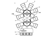
- FIG. 3 is a schematic configuration diagram of the substrate processing system 1 including the substrate cooling apparatus 100 according to the present embodiment.
- the substrate processing system 1 is a cluster-type apparatus, and includes a plurality of substrate processing chambers 2, a load lock chamber 4, a substrate cooling apparatus 100 according to this embodiment, and a temperature raising apparatus 200.
- the plurality of substrate processing chambers 2 may perform the same processing on the substrate S or may perform different processing.
- the plurality of substrate processing chambers 2, the load lock chamber 4, the substrate cooling device 100, and the temperature raising device 200 are connected via the transfer chamber 3, and a gate valve that can be opened and closed is provided at each connection portion. It has been.
- a transfer robot 7 is provided in the transfer chamber 3. By driving the transfer robot 7, the substrate processing chamber 2, the load lock chamber 4, the substrate cooling device 100, and the temperature raising device 200 are arranged in a predetermined processing order.
- the substrate S is transferred.
- Each substrate processing chamber 2, transfer chamber 3, substrate cooling apparatus 100, and temperature raising apparatus 200 is provided with an exhaust pump, and the substrate S can be transferred between the chambers while maintaining a vacuum.
- An autoloader 5 for supplying the substrate S is provided outside the load lock chamber 4.
- the autoloader 5 is configured to take out the substrates one by one from the external cassette 6 in which a plurality of substrates are stored on the atmosphere side and store them in the load lock chamber 4.
- FIG. 4 is a schematic diagram showing a configuration of an exemplary MTJ (Magnetic Tunnel Junction) element 1000 that performs the film forming method according to the present embodiment.
- the MTJ element is used for, for example, an MRAM (Magnetic Random Access Memory), a magnetic sensor, or the like.
- the MTJ element 1000 is a perpendicular magnetization type MTJ element (p-MTJ element).
- the MTJ element 1000 includes a lower electrode 1002, a Ta layer (seed layer) 1003, a CoFeB layer 1006 as a free layer (magnetization free layer), and an MgO layer (tunnel barrier layer) 1007 on a substrate 1001 in this order.
- the MTJ element 1000 further includes a CoFeB layer 1008 as a reference layer (magnetization fixed layer), a Ta layer 1009, a stacked body 1010, a Ta layer (cap layer) 1011 and an upper electrode 1012 in this order.
- a stacked body 1010 (pinned layer) of the MTJ element 1000 is obtained by alternately stacking a predetermined number N of Co layers and Pt layers.
- the MTJ element 1000 is not limited to the configuration shown here, and arbitrary changes such as increase / decrease of layers, change of constituent materials of each layer, and reversal of the upper and lower stacking order were performed within the range not impairing the function of the perpendicular magnetization type element.
- a configuration can be used.
- the configuration of the MTJ element 2000 in which the upper and lower stacking order of the MTJ element 1000 described above is reversed may be used.
- the cooling process using the substrate cooling apparatus 100 is performed after the tunnel barrier layer (MgO layer) 1007 is formed on the free layer (CoFeB layer) 1006, and the tunnel barrier layer (MgO layer) 1007. It is preferably performed before the CoFeB layer 1008 of the reference layer is formed thereon.
- the interface steepness between the tunnel barrier layer 1007 and the CoFeB layer 1008 of the reference layer can be improved by the cooling, and the surface of the tunnel barrier layer 1007 is cooled. That is, contamination of the tunnel barrier layer 1007 and the CoFeB layer 1008 can be suppressed.
- the cooling process using the substrate cooling apparatus 100 may be performed at other timings.
- the MR ratio may be increased even after the Ta layer 1003 is formed or the CoFeB layer 1006 is formed as a free layer (magnetization free layer). Improvement can be expected. This is because it is effective if the substrate is in a cooled state when the CoFeB layer 1008 of the reference layer is formed.
- the cooling process may be performed at a plurality of timings among the above timings.
- the temperature raising process using the temperature raising device 200 is after the alignment separation layer (Ta layer) 1009 on the CoFeB layer 1008 of the reference layer is formed, It is preferably performed before the stacked body 1010 is formed.
- the temperature raising process is performed using the temperature raising device 200 at this timing, the magnetic properties of the stacked body 1010 can be improved by heating. Furthermore, since the temperature of the substrate rises above the dew point, dew condensation on the substrate can be suppressed when the substrate is unloaded from the substrate processing system 1.
- the temperature raising process may be performed at any timing after the CoFeB layer 1008 of the reference layer is formed and before the stacked body 1010 is formed.
- the temperature raising process may be performed after the CoFeB layer 1008 as the reference layer is formed and before the alignment separation layer (Ta layer) 1009 is formed.
- the stacked body 1010 is a layer having perpendicular magnetic anisotropy (PMA) that is easily magnetized in one direction (a direction perpendicular to the film surface), and is called a pinned layer or a PMA layer.
- PMA perpendicular magnetic anisotropy
- the perpendicular magnetic anisotropy of the stacked body 1010 is larger, the deterioration of the thermal disturbance resistance of the reference layer can be suppressed, and unintended magnetization reversal of the reference layer can be prevented.
- FIG. 5 is a view showing a flowchart of the film forming method according to the present embodiment.
- the film forming method according to the present embodiment will be described using the cluster-type substrate processing system 1 shown in FIG. 3, but the present invention is not limited to this.
- an inline type substrate processing system may be used.
- the substrate cooling apparatus 100 shown in FIG. 1 is used as the substrate cooling apparatus included in the substrate processing system 1, but any other substrate cooling apparatus may be used.
- another device may be used instead of the temperature raising device 200.
- the substrate S is carried into the load lock chamber 4 of the substrate processing system 1 (step S11).
- the substrate S is moved to the predetermined substrate processing chamber 2, and a lower layer film forming process is performed (step S12).
- impurities and the like attached on the substrate are removed by an etching method, and then the lower electrode 1002, Ta layer 1003, and free film on the substrate 1001, in the MTJ element 1000, a film below the MgO layer 1007.
- a CoFeB layer 1006 as a layer is sequentially formed by a sputtering method.
- an MgO layer 1007 as a tunnel barrier layer in the MTJ element 1000 is formed.
- the MgO layer 1007 is formed by a radio frequency (RF) sputtering method using an MgO target.
- RF radio frequency
- a Mg layer may be formed on the CoFeB layer 1006 as a free layer by a sputtering method using an Mg target, and then the Mg layer may be oxidized.
- the film formation process and the oxidation process may be performed in the same substrate processing chamber 2 or may be performed in different substrate processing chambers 2.
- the substrate S is moved to the substrate cooling apparatus 100, and the second step (cooling step) is performed (step S14).
- the substrate S on which the MgO layer 1007 is formed is cooled to a temperature of 200K or lower (in this embodiment, 100K).
- a temperature of 200K or lower in this embodiment, 100K.
- the substrate cooling apparatus 100 is used to perform a cooling process.
- the cooling process according to the present embodiment is not limited to this, and any cooling device configuration and cooling process can be performed as long as the substrate S on which the MgO layer 1007 is formed can be cooled to a predetermined temperature.
- a method may be used.
- analysis of structural components, such as the formed CoFeB layer 1008, can be performed by, for example, an X-ray diffraction method.
- step S15 by driving the transfer robot 7 of the transfer chamber 3, the substrate S is moved to the predetermined substrate processing chamber 2, and the third step is performed (step S15).
- a CoFeB layer 1008 as a reference layer in the MTJ element 1000 and a Ta layer 1009 on the CoFeB layer 1008 are sequentially formed by a sputtering method.
- the substrate S is moved to the temperature raising device 200, and the fourth step (temperature raising step) is performed (step S16).
- the temperature raising step the temperature of the substrate S on which the layers up to the Ta layer 1009 are formed is raised to a temperature equal to or higher than the dew point temperature (293 K in this embodiment).
- a film above the stacked body 1010 in the MTJ element 1000 that is, a stacked body 1010 as a pinned layer, a Ta layer 1011 and an upper electrode 1012 are sequentially formed by sputtering.
- the magnetic properties of the stacked body 1010 formed on the Ta layer 1009 can be improved.
- the magnetic characteristics of the stacked body 1010 refer to perpendicular magnetic anisotropy that is easily magnetized in one direction (direction perpendicular to the film surface).
- the reason why the magnetic properties of the stacked body 1010 are improved by raising the temperature is that Co atoms sputtered and deposited on the substrate when forming the stacked body 1010 are likely to migrate on the adhered surface. Seem. That is, it is considered that the positional relationship between Pt and Co in the laminated body 1010 becomes more preferable as the Co particles move on the surface.
- the effect of improving the magnetic properties of the laminate 1010 will be described later. Even if the laminate has a film structure that does not use Co atoms, the same effect can be expected by applying the film forming method (manufacturing method) of the present embodiment as long as it is an atom that easily migrates on the attached surface.
- an annealing process is performed at a predetermined temperature (for example, 150 to 400 degrees), and the film formation is completed (step S18).
- the film forming process and the annealing process may be performed in the same substrate processing chamber 2 or may be performed in different substrate processing chambers 2.
- the substrate S is moved to the transfer position (substrate unloading position) in the load lock chamber 4 by driving the transfer robot 7 of the transfer chamber 3 (step S19). Thereafter, the substrate S is sent to a downstream process of the substrate processing system 1.
- the annealing process may be performed by an apparatus different from the substrate processing system 1. In this case, an annealing process is performed as a process downstream of the substrate processing system 1.
- Each layer formed in the film formation process (steps S12, S13, S15, and S17) of this embodiment is formed by a sputtering method, but may be formed by any other film formation method.
- two or more films may be formed in the same substrate processing chamber 2, and all the films are different from each other.
- a film may be formed in the chamber 2.
- At least one of the film forming steps (steps S12, S13, S15, and S17) and the cooling step (step S14) or the temperature raising step (step S16) may be performed in the same chamber.
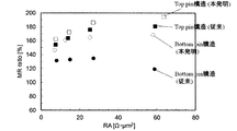
- FIG. 6 is a diagram showing an MR ratio with respect to RA (area resistance) of an MTJ element manufactured by using the film forming method according to the present embodiment.
- An MTJ element manufactured using the film forming method according to this embodiment and an MTJ element manufactured using a conventional film forming method were manufactured, and the RA and MR ratio were measured.
- the conventional film-forming method is manufactured according to the flowchart of FIG. 5 or FIG. 10, but is manufactured without performing the cooling process (steps S 14 and 34) and the temperature raising process (steps S 16 and 36). Refer to the membrane method.
- the horizontal axis in FIG. 6 is RA ( ⁇ ⁇ ⁇ m 2 ), and the vertical axis is the MR ratio (%). It can be said that the lower the RA and the higher the MR ratio, the better the element characteristics of the MTJ element.
- square color painting ( ⁇ ) is a measurement result of the MTJ element having the top pin structure shown in FIG. 4 manufactured by the conventional film forming method.
- the square color removal ( ⁇ ) is the measurement result of the MTJ element having the top pin structure manufactured by the film forming method according to this embodiment.
- round color removal ( ⁇ ) and the round color painting ( ⁇ ) in FIG. 6 are the measurement results of the MTJ element having the bottom pin structure.
- the round color coating ( ⁇ ) is a measurement result of an MTJ element having a bottom pin structure manufactured by a conventional film forming method.
- a round color ( ⁇ ) is a measurement result of an MTJ element having a bottom pin structure manufactured by a film forming method according to a second embodiment described later.
- the MTJ element 2000 will be described later with reference to FIGS.
- the MR ratio is improved as compared with the conventional case where the cooling and heating process is not performed.
- the MR ratio with respect to RA area resistance
- the cooling process step S14
- the presence or absence of the temperature raising process step S16
- cooling is performed after the formation of the MgO layer 1007 as the tunnel barrier layer and before the formation of the CoFeB layer 1008 as the reference layer. It was confirmed to be effective.
- the RA and MR ratio of the MTJ element that was not subjected to the temperature raising step (step S36) almost overlapped with the point of the round color ( ⁇ ). That is, the RA (area resistance) and the MR ratio are greatly affected by the cooling process (step S34) also for the MTJ element having the bottom pin structure.
- it is effective to perform cooling after the formation of the MgO layer 2008 as a tunnel barrier layer and before the formation of the CoFeB layer 2009 as a free layer. It was confirmed.
- FIG. 7 is a diagram showing the effect of the cooling step in the film forming method according to the present embodiment, and is a diagram showing a graph of the MR ratio against the B content (boron content) in the CoFeB layer as the reference layer in the MTJ element. It is.
- the B ratio in the CoFeB layer 1008 as the reference layer was variously changed, and the MR ratio was measured.
- the horizontal axis of FIG. 7 is the B content (at%) in the CoFeB layer as the reference layer 1008, and the vertical axis is the MR ratio (%).
- the triangular coloring ( ⁇ ) is the measurement result of the MTJ element formed without cooling, and the triangular coloring ( ⁇ ) is after the deposition of the MgO layer 1007 and is a reference. It is a measurement result of the MTJ element formed by cooling before forming the CoFeB layer 1008 as a layer.
- the MTJ element according to any measurement result was manufactured according to the flowchart of FIG. 5, but none of the temperature raising step (step S ⁇ b> 16) was performed.
- An MTJ element represented by a triangular color ( ⁇ ) and an MTJ element represented by a triangular color ( ⁇ ) differ only in the presence or absence of a cooling step (step S14).
- step S16 since the presence or absence of the temperature raising step (step S16) does not have a great influence on the MR ratio, the measurement result of the MTJ element manufactured by the manufacturing method of the present embodiment that performs the temperature raising step performs the cooling step in FIG. This is almost the same as the measurement result of the film forming method.
- the measurement result of the film forming method for performing the cooling process is the measurement result when the cooling is not performed at any B content (triangle color). It can be seen that an MR ratio higher than that of paint ( ⁇ ) is realized.
- the MR ratio increased as the B content decreased. Therefore, according to the film forming method according to the present embodiment, it is possible to set the B content lower than the conventional one while maintaining a high MR ratio, and the degree of freedom of the composition of the CoFeB layer 1008 as the reference layer. Is expensive.
- the MR ratio can be improved when the reference layer has an amorphous phase.
- B in order to make a conventional CoFeB layer into an amorphous phase, it is necessary to add B in a predetermined ratio (about 20% as described above).
- the film forming method according to the present embodiment realizes a higher MR ratio with a lower B content than in the prior art after the tunnel barrier layer is formed and before the reference layer is formed. This is probably because an amorphous phase is easily formed in the reference layer.
- the reference layer has an amorphous phase even at a low B content, and a high MR ratio is realized.
- the MTJ element having the bottom pin structure the MTJ element 2000 having a high MR ratio is manufactured by cooling after the formation of the MgO layer 2008 and before the formation of the CoFeB layer 2009 as a free layer. it can.
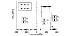
- FIG. 8 is a magnetization resistance curve of the MTJ element manufactured by the film forming method according to this embodiment.
- the MTJ element used for the measurement was manufactured in accordance with the MTJ element (rectangular color coating ( ⁇ )) manufactured by the film forming method according to the present embodiment (the temperature increasing step was performed) and the flowchart of FIG.
- MTJ elements that were not subjected to the temperature raising step (round colored coating ( ⁇ )) were compared and measured.
- the horizontal axis is the direction and strength of the magnetic field strength in the vertical direction
- -400 (Oe) is the downward (magnetization direction of the reference layer) and the magnetic field is 400 (Oe)
- 400 (Oe) is the upward (reference) Direction opposite to the magnetization direction of the layer).
- the vertical axis represents the resistance value.
- the resistance value on the vertical axis is a value proportional to the MR ratio.
- the magnetization of the free layer was reversed at 80 (Oe), and the magnetization of the reference layer was reversed at 280 (Oe).
- the magnetization of the free layer was reversed at 80 (Oe)
- the magnetization of the reference layer was reversed at 320 (Oe). That is, it can be seen that the reference layer of the MTJ element subjected to the temperature raising process has high resistance to a magnetic field, and magnetization reversal hardly occurs.
- the manufacturing method of the present embodiment it is possible to manufacture a magnetoresistive effect element that has a higher MR ratio than the conventional one, and does not decrease the perpendicular magnetic anisotropy of the reference layer and can suppress the decrease in MR ratio.
- the magnetoresistive effect element manufactured by the manufacturing method of the present embodiment has a higher MR ratio than the conventional one, and can suppress the deterioration of the thermal disturbance resistance of the reference layer. The occurrence of inversion can be prevented.
- the MTJ element 1000 has a structure having a reference layer 1008 on the tunnel barrier layer 1007 (top pin structure), but also has a structure having a free layer on the tunnel barrier layer (bottom pin structure).
- the present invention can be applied.
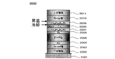
- FIG. 10 is a flowchart illustrating a method of forming the MTJ element 2000 shown in FIG. 9 as an example of an MTJ element having a bottom pin structure.
- the layers up to the CoFeB layer 2007 as a reference layer are formed in the lower layer formation step (step S32). That is, in the manufacturing process of the MTJ element 2000, the lower electrode 2002, the Ta seed layer 2003, the Ru layer 2004, the stacked body 2005 (pinned layer), the Ta layer 2006, and the reference are formed on the substrate 1001 in the lower layer deposition process (step S32).
- a CoFeB layer 2007 is formed as a layer.
- the laminated body (pinned layer) is formed before the tunnel barrier layer (MgO layer).
- step S33 In the first step (step S33) after the lower layer formation step (step S32), an MgO layer 2008 as a tunnel barrier layer is formed on the CoFeB layer 2007 as a reference layer. Then, the second process (cooling process: step S34) is performed, and the CoFeB layer 2009 as a free layer is formed on the MgO layer 2008 in the third process (step S35). After the third step (step S35), the fourth step (temperature raising step: step S36) is performed, and the Ta cap layer 2010 and the upper electrode 2011 are formed on the CoFeB layer 2009 in the fifth step (step S37). Then, the film formation is finished (step S38), and the substrate is carried out (step S39).
- the film forming method according to the present invention can be applied to both a top pin structure and a bottom pin structure, and forms either a free layer or a reference layer and forms a tunnel barrier layer on one of the free layer and the reference layer. Then, cooling is performed, the other of the free layer and the reference layer is formed on the tunnel barrier layer, and the temperature is further raised.
- the manufacturing method (film forming method) of the present invention it is possible to manufacture a magnetoresistive effect element having a higher MR ratio than before.
- the substrate after the temperature raising process has a temperature exceeding the dew point temperature, and thus adhesion of moisture and the like can be suppressed.
- the dew point temperature here means a temperature at which moisture begins to condense, and moisture does not condense on the substrate at a temperature exceeding the dew point temperature.
- dew condensation on the substrate can be suppressed when the substrate is unloaded from the substrate processing system 1.
- the magnetoresistive element having a top pin structure manufactured by the manufacturing method of the present invention has a higher MR ratio than the conventional one and can suppress a decrease in the thermal disturbance resistance of the reference layer. Unintended magnetization reversal can be prevented from occurring.
- the present invention is not limited to the above-described embodiment, and can be appropriately changed without departing from the spirit of the present invention.
- Each of the above embodiments has been described as being applied to the manufacture of an MTJ element (TMR element) used in an MRAM.
- TMR element MTJ element
- the same cooling method, temperature raising method, and film forming method can be used for other MTJ elements. Applicable to manufacturing.
- the direction of gravity is described as the vertical direction, but the direction in which the apparatus is configured is arbitrary.
- the vertical direction in each of the above-described embodiments is What is necessary is just to read as a direction perpendicular
Landscapes
- Engineering & Computer Science (AREA)
- Chemical & Material Sciences (AREA)
- Crystallography & Structural Chemistry (AREA)
- Nanotechnology (AREA)
- Power Engineering (AREA)
- Manufacturing & Machinery (AREA)
- Physics & Mathematics (AREA)
- Spectroscopy & Molecular Physics (AREA)
- Hall/Mr Elements (AREA)
- Mram Or Spin Memory Techniques (AREA)
- Physical Vapour Deposition (AREA)
- Thin Magnetic Films (AREA)
Abstract
本発明は、従来よりも高いMR比を有する磁気抵抗効果素子の製造方法を提供する。本発明の一実施形態に係る磁気抵抗効果素子の製造方法は、磁化自由層および磁化固定層の一方が表面に形成された基板上にトンネルバリア層を形成する工程S13と、トンネルバリア層を形成する工程の後に、基板を冷却する工程S14と、冷却する工程の後に、トンネルバリア層上に磁化自由層および磁化固定層の他方を形成する工程S15と、磁化自由層および磁化固定層の他方を形成する工程の後に、基板を昇温する昇温工程S16とを備える。
Description
本発明は、磁気抵抗効果素子の製造方法に係り、特にMRAMに用いられるTMR素子に好適な製造方法に関する。
磁場によって電気抵抗が変化する磁気抵抗効果素子として、TMR(Tunnel Magneto Resistance)効果を利用して情報の記憶や磁気の検出を行うTMR素子(MTJ素子ともいう)が知られている。近年、MRAM等へのMTJ素子の利用が期待されている。
非特許文献1には、垂直磁化型のMTJ素子が開示されている。垂直磁化型のMTJ素子は、フリー層(磁化自由層)、トンネルバリア層、およびリファレンス層(磁化固定層)が積層された構造を含み、フリー層およびリファレンス層の磁化方向はそれぞれ積層方向と平行になっている。
磁気抵抗効果素子を用いたMRAMデバイスの特性の向上のためには、MR比(磁気抵抗比)を高くすることが重要である。非特許文献1に記載のCoFeB/MgO/CoFeBからなる積層構造は100%を超える高いMR比を示すことが知られている。
D. C. Worledge et al., "Spin torque switching of perpendicular Ta|CoFeB|MgO-based magnetic tunnel junctions", Appl. Phys. Lett. 98, 2011, 022501
しかしながら、非特許文献1に記載の磁気抵抗効果素子であっても、十分に高いMR比とはいえない。磁気抵抗効果素子の構造を変更することによってMR比をさらに高める研究がなされている一方で、構造ではなく製造方法を変更することによってMR比を高めることも求められている。
本発明は、上述の問題点を解決するためになされたものであって、従来よりも高いMR比を有する磁気抵抗効果素子の製造方法を提供することを目的とする。
本発明の一態様は、磁気抵抗効果素子の製造方法であって、表面に磁化自由層および磁化固定層の一方が形成された基板上にトンネルバリア層を形成する第1工程と、前記第1工程の後に、前記基板を冷却する第2工程と、前記第2工程の後に、前記トンネルバリア層上に前記磁化自由層および前記磁化固定層の他方を形成する第3工程と、前記第3工程の後に、前記基板を昇温する第4工程と、を備えることを特徴とする。
本発明に係る磁気抵抗効果素子の製造方法によれば、トンネルバリア層を形成する工程の後であって、トンネルバリア層上に磁化自由層又は磁化固定層を形成する工程の前に、基板を冷却する工程を行うことによって、高いMR比を有する磁気抵抗効果素子を実現することができる。また、本発明に係る磁気抵抗効果素子の製造方法によれば、トンネルバリア層を形成する工程の後であって、トンネルバリア層上に磁化自由層(フリー層)又は磁化固定層(リファレンス層)を形成する工程の後に、基板を昇温する工程を行うことによって、基板上への結露を防ぎ歩留まりを向上することができる。
以下、図面を参照して、本発明の実施の形態を説明するが、本発明は本実施形態に限定されるものではない。なお、以下で説明する図面で、同機能を有するものは同一符号を付け、その繰り返しの説明は省略することもある。
(第1実施形態)
図1は、本実施形態に係る基板の冷却を行う基板処理装置としての基板冷却装置100を示す概略構成図である。基板冷却装置100はチャンバ101と排気チャンバ119とを備えている。チャンバ101の上壁101aは取り外し可能に設けられており、上壁101aを取り外してメンテナンス、クリーニング等を行うことができる。チャンバ101の側壁101bには開閉可能なゲートバルブ102が設けられており、ゲートバルブ102を介して基板Sをチャンバ101の内外に搬送可能である。チャンバ101内には基板載置面103aを有する基板ホルダ103が設けられており、基板載置面103a上には基板Sを載置可能である。
図1は、本実施形態に係る基板の冷却を行う基板処理装置としての基板冷却装置100を示す概略構成図である。基板冷却装置100はチャンバ101と排気チャンバ119とを備えている。チャンバ101の上壁101aは取り外し可能に設けられており、上壁101aを取り外してメンテナンス、クリーニング等を行うことができる。チャンバ101の側壁101bには開閉可能なゲートバルブ102が設けられており、ゲートバルブ102を介して基板Sをチャンバ101の内外に搬送可能である。チャンバ101内には基板載置面103aを有する基板ホルダ103が設けられており、基板載置面103a上には基板Sを載置可能である。
基板ホルダ103には基板載置面103aを貫通して基板Sの裏面を支持するための棒状のリフトピン104が設けられており、リフトピン104はリフトピン駆動機構105によって基板Sまたは基板載置面103aの法線方向に沿って上昇および下降可能である。また、基板ホルダ103には基板Sの表面の外周部を固定するためのメカニカルチャック106が設けられており、メカニカルチャック106はメカニカルチャック駆動機構107によって基板Sまたは基板載置面103aの法線方向に沿って上昇および下降可能である。リフトピン駆動機構105およびメカニカルチャック駆動機構107は、モータ、アクチュエータ等の任意の駆動手段である。リフトピン104とリフトピン駆動機構105との間、およびメカニカルチャック106とメカニカルチャック駆動機構107との間には、チャンバ101の密閉状態を保ったままリフトピン104およびメカニカルチャック106を移動できるように、伸縮可能なベローズ108が設けられている。
基板Sを固定するために、メカニカルチャック106およびメカニカルチャック駆動機構107の代わりに、静電力により基板Sを基板ホルダ103に固定する静電吸着機構(ESC)を設けてもよい。
基板ホルダ103には、チャンバ101の下壁101cを貫通する基板ホルダ支柱110を介して、チャンバ101の外部に設けられている基板ホルダ冷却部109(基板ホルダ冷却手段)が接続されている。基板ホルダ冷却部109を用いて基板ホルダ103を低温に維持することによって、基板載置面103aに載置された基板Sを冷却可能である。基板ホルダ冷却部109は、基板ホルダ103の温度を測定するための不図示の温度測定部(例えば、熱電対)を有する。基板ホルダ103および基板ホルダ支柱110は、熱伝導性の高い金属、例えば銅またはアルミニウムを用いて作製されていることが望ましい。
チャンバ101内において、シールド111が設けられている。シールド111は基板ホルダ103の側方を取り囲むとともに、基板ホルダ103の上方を覆うように設けられている。すなわち、シールド111は、基板載置面103aの側方を取り囲むとともに、基板載置面103aに対向するように設けられている。
シールド111には、チャンバ101の上壁101aを貫通するシールド支柱113を介して、チャンバ101の外部に設けられているシールド冷却部112が接続されている。シールド冷却部112を用いてシールド111を低温に維持することによって、基板Sの搬送時に基板ホルダ103から放出される気体分子がシールド111の表面に到達した際に、表面に該気体分子をトラップすることができる。シールド冷却部112は、シールド111の温度を測定するための不図示の温度測定部(例えば、熱電対)を有する。シールド111およびシールド支柱113は、熱伝導性の高い金属、例えば銅またはアルミニウムを用いて作製されていることが望ましい。
基板ホルダ冷却部109およびシールド冷却部112(シールド冷却手段)は、任意の方法により冷却を行うための冷却手段であり、例えばヘリウムの断熱膨張を利用して冷却を行う冷却装置(例えば、Gifford-McMahon冷凍機やスターリング冷凍機など)であってよく、または冷媒として外部から供給される低温の液体窒素等の冷媒を流すことにより冷却を行う装置であってよい。本実施形態では基板ホルダ冷却部109とシールド冷却部112とは別個の部材として設けられているが、単一の冷却部として設けられてもよい。シールド111の側面におけるゲートバルブ102に対向する部分には、基板Sが通るための開口部114が設けられている。シールド111に付着したガスは、チャンバ101および排気チャンバ119の各所に設けられているヒータ116で加熱することによって除去することができる。
チャンバ101には、それぞれの内部空間が連通するように排気チャンバ119が接続されている。排気チャンバ119にはチャンバ101内を真空排気可能な排気部としての排気ポンプ120が設けられている。排気ポンプ120としては、必要とする真空度に応じてドライポンプ、ターボ分子ポンプ等の任意の排気手段を用いることができ、それらを組み合わせて用いてもよい。さらに、チャンバ101にはシールド111内、すなわちシールド111により区画される空間内の圧力を測定するためのシールド内真空計121が設けられており、排気チャンバ119には排気チャンバ119内の圧力を測定するためのチャンバ内真空計122が設けられている。
さらに、基板冷却装置100には、基板Sの冷却を効率的に行うために、基板Sの裏面と基板載置面103aとの間に冷却ガスを導入するための冷却ガス導入部123が設けられている。冷却ガス導入部123は冷却ガスが通るための管であるガスライン124に接続されており、ガスライン124はチャンバ101および基板ホルダ103を貫通して基板Sの裏面と基板載置面103aとの間の空間に開口している。冷却ガス導入部123から導入される冷却ガスとしてはHe、Arまたはそれらの少なくとも一方を含む混合ガスを用いることができ、冷却ガスが基板Sの裏面に行き渡ることで基板Sを素早く均一に冷却することができる。ガスライン124はさらに排気ポンプ120に接続されており、排気ポンプ120を駆動することによって使用後の冷却ガスを排気することができる。ガスライン124は不図示の可変バルブを備えており、経路や流量を変更可能である。
図1ではガスライン124は1系統のみ示されているが、冷却ガス導入部123から冷却ガスを導入するためのガスラインと冷却ガスを排気するためのガスラインとの2系統が別個に設けられてもよい。冷却ガス導入部123は、マスフロー制御器(MFC)、自動圧力制御器(APC)等のガス流量調整手段を備えていることが望ましい。なお、冷却ガス導入部123は必ずしも設けられなくともよく、上述の冷却ガスを用いず、基板Sを冷却された基板載置面103aに直接載置しても基板Sを冷却できることはもちろんである。
ガスライン124の近傍には、ガスラインヒータ125が設けられている。ガスラインヒータ125によってガスライン124を加熱することによって、ガスラインの内面に吸着される気体分子を効率的に除去することができる。ガスラインヒータ125は、図1ではガスライン124の一部にのみ設けられているが、ガスライン124の全体に設けられてもよい。ガスラインヒータ125としては、任意の加熱手段を用いてよいが、例えばリボンヒータを用いることができる。
図2は、本実施形態に係る基板の昇温を行う基板処理装置としての昇温装置200を示す概略構成図である。昇温装置200は、基板に昇温処理を施す装置であり、チャンバ201と、排気装置202と、ガス供給装置203と、基板ホルダ204を有している。昇温装置200は、後述の搬送チャンバ3とゲートバルブ205を介して連結されている。ガス供給装置203は例えば、ガスボンベに連結されたガス流通路とチャンバ201内にガスを供給するガス供給口203aと不図示のマスフローコントローラ(MFC)とからなる。基板ホルダ204に基板を載置した状態で、ガス供給口203aから昇温ガスを導入することで基板を昇温することができる。このとき、ガス供給装置203から導入される昇温ガスは予め温度を調整しておくと好適である。予め調整しておくガスの温度は、水分が結露しない温度(露点温度)以上の温度が望ましく、温度幅としては283K~343Kの範囲が好ましい。本実施形態のガスの温度は室温(293K程度)とされている。昇温ガスとしては、水分の少ないガスが好適であり、例えば、窒素ガスやドライエア若しくはアルゴンガスやヘリウムガスを用いることができる。
基板の昇温が終了したら排気装置202でチャンバ201内のガスを排気した後、基板は搬送チャンバ3が有する搬送装置7(搬送ロボット)によって次の工程のチャンバに搬送される。昇温装置200では、ガスで基板を昇温する方式したが、ランプヒータや基板ホルダを加熱することで基板を昇温してもよい。本実施形態においては昇温装置200を用いたが、基板を昇温することができる構成であれば他の方法を用いてもよい。例えば、搬送経路のいずれかに基板を昇温するヒータを設けて、搬送中の基板をヒータで昇温してもよい。或いは、昇温装置200に替えてロードロックチャンバを用いてもよい。ロードロックチャンバで基板を昇温させる場合は、導入されるガスで基板を昇温した後に後工程の成膜を行うチャンバに搬送される。ここでの昇温処理は、露点温度以上に基板温度を上昇させる処理であり、本実施形態の昇温装置200では基板を室温(293K)に昇温させている。
図3は、本実施形態に係る基板冷却装置100を備える基板処理システム1の概略構成図である。基板処理システム1はクラスタ型の装置であり、複数の基板処理チャンバ2と、ロードロックチャンバ4と、本実施形態に係る基板冷却装置100と、昇温装置200とを備えている。複数の基板処理チャンバ2は基板Sに対して同一の処理を行うものであってもよく、または異なる処理を行うものであってもよい。
複数の基板処理チャンバ2と、ロードロックチャンバ4と、基板冷却装置100と、昇温装置200とは搬送チャンバ3を介して接続されており、それぞれの接続部分には開閉可能なゲートバルブが設けられている。搬送チャンバ3には搬送ロボット7が設けられており、搬送ロボット7を駆動させることによって各基板処理チャンバ2、ロードロックチャンバ4、基板冷却装置100および昇温装置200の間で所定の処理順にしたがって基板Sが搬送される。各基板処理チャンバ2、搬送チャンバ3、基板冷却装置100および昇温装置200にはそれぞれ排気ポンプが設けられており、真空を保ったままチャンバ間で基板Sを搬送可能である。ロードロックチャンバ4の外側には、基板Sを供給するためのオートローダ5が設けられている。オートローダ5は、大気側において複数の基板が収納されている外部カセット6から基板を一枚ずつ取り出し、ロードロックチャンバ4内に収容するように構成されている。
図4は、本実施形態に係る成膜方法を行う例示的なMTJ(Magnetic Tunnel Junction:磁気抵抗効果素子)素子1000の構成を示す模式図である。MTJ素子は、例えばMRAM(Magnetic Random Access Memory)、磁気センサ等に用いられる。
MTJ素子1000は、垂直磁化型MTJ素子(p-MTJ素子)である。MTJ素子1000は、基板1001上に下部電極1002と、Ta層(シード層)1003と、フリー層(磁化自由層)としてのCoFeB層1006と、MgO層(トンネルバリア層)1007とを順に備える。MTJ素子1000は、さらにその上に、リファレンス層(磁化固定層)としてのCoFeB層1008と、Ta層1009と、積層体1010と、Ta層(キャップ層)1011と、上部電極1012とを順に備える。MTJ素子1000の積層体1010(ピン層)は、Co層とPt層とを交互に所定の数Nだけ積層したものである。
MTJ素子1000としてはここに示した構成に限られず、垂直磁化型素子の機能を損なわない範囲で層の増減、各層の構成材料の変更、上下の積層順の逆転等の任意の変更を行った構成を用いることができる。例えば、図9を用いて後述する第2実施形態のように、上述のMTJ素子1000の上下の積層順を逆転したMTJ素子2000の構成を用いてもよい。
本実施形態に係る基板冷却装置100を用いる冷却処理は、フリー層(CoFeB層)1006上にトンネルバリア層(MgO層)1007が成膜された後であって、トンネルバリア層(MgO層)1007の上にリファレンス層のCoFeB層1008が成膜される前に行われることが好ましい。このタイミングで基板冷却装置100を用いて冷却処理を行うと、冷却によりトンネルバリア層1007とリファレンス層のCoFeB層1008の界面急峻性を向上させることができ、かつ冷却中にトンネルバリア層1007の表面(すなわち、トンネルバリア層1007とCoFeB層1008との間の界面)が汚染されることを抑えることができる。
基板冷却装置100を用いる冷却処理は、その他のタイミングで行われてよく、例えば、Ta層1003の成膜後や、フリー層(磁化自由層)としてのCoFeB層1006の成膜後でもMR比の向上が期待できる。リファレンス層のCoFeB層1008の成膜時に基板が冷却された状態であれば効果があるためである。また、上記のタイミングのうち、複数のタイミングで冷却処理が行われてもよい。
本実施形態に係る昇温装置200を用いる昇温処理は、リファレンス層のCoFeB層1008上の配向分離層(Ta層)1009を成膜した後であって、配向分離層(Ta層)1009の上に積層体1010が成膜される前に行われることが好ましい。このタイミングで昇温装置200を用いて昇温処理を行うと、加熱により積層体1010の磁気特性を向上させることができる。さらに、昇温処理によって基板は露点温度以上になるため、基板処理システム1から基板を搬出したときに基板への結露を抑えることができる。
なお、昇温処理は、リファレンス層のCoFeB層1008を成膜した後であって、積層体1010が成膜される前の任意のタイミングで行ってもよい。例えば、リファレンス層のCoFeB層1008の成膜後であって、配向分離層(Ta層)1009の成膜前に昇温処理を行ってもよい。ここで積層体1010は、ひとつの方向(膜面に対して垂直な方向)に磁化されやすい垂直磁気異方性(PMA)を持つ層をいい、ピン層若しくはPMA層と言い換えられる。積層体1010の垂直磁気異方性が大きいほど、リファレンス層の熱擾乱耐性の低下を抑えられ、リファレンス層の意図しない磁化反転の発生を防ぐことができる。
図5は、本実施形態に係る成膜方法のフローチャートを示す図である。ここでは図3に示すクラスタ型の基板処理システム1を用いて本実施形態に係る成膜方法の説明を行うが、これに限られるものではない。例えば、インライン型の基板処理システムを用いてもよい。また、本実施形態では基板処理システム1に含まれる基板冷却装置として図1に示す基板冷却装置100を用いるが、その他任意の基板冷却装置を用いてもよい。同様に、昇温装置200に替えて他の装置を用いてもよい。
まず、基板処理システム1のロードロックチャンバ4に基板Sを搬入する(ステップS11)。次に、搬送チャンバ3の搬送ロボット7を駆動させることによって、所定の基板処理チャンバ2に基板Sを移動し、下層成膜工程を行う(ステップS12)。下層成膜工程では、エッチング法によって基板上に付着した不純物等を除去し、その後にMTJ素子1000のうちMgO層1007より下の膜、すなわち基板1001上に下部電極1002、Ta層1003、およびフリー層としてのCoFeB層1006を順にスパッタリング法によって成膜する。
次に、搬送チャンバ3の搬送ロボット7を駆動させることによって、所定の基板処理チャンバ2に基板Sを移動し、第1工程を行う(ステップS13)。第1工程では、MTJ素子1000のうちトンネルバリア層としてのMgO層1007を成膜する。MgO層1007は、MgOターゲットを用いた高周波(RF)スパッタリング法によって成膜されている。別の方法として、Mgターゲットを用いたスパッタリング法によってフリー層としてのCoFeB層1006の上にMg層を成膜し、その後に該Mg層に対して酸化処理を行うことによって形成してもよい。成膜処理と酸化処理とは同じ基板処理チャンバ2内で行われてもよく、異なる基板処理チャンバ2内で行われてもよい。
次に、搬送チャンバ3の搬送ロボット7を駆動させることによって、基板冷却装置100に基板Sを移動し、第2工程(冷却工程)を行う(ステップS14)。冷却工程では、MgO層1007が成膜された基板Sを200K以下の温度(本実施形態では100K)まで冷却する。200K以下の温度まで基板Sを冷却することによって、この後に成膜されるリファレンス層としてのCoFeB層1008中にアモルファス相を形成しやすくすることができる。
冷却工程においては、基板冷却装置100を用いて冷却処理を行う。これにより、基板Sの冷却を素早く行いかつ膜中の不純物を低減するという追加の効果を得ることができる。本実施形態に係る冷却工程はこれに限られるものではなく、MgO層1007が成膜された基板Sを所定の温度まで冷却することが可能であれば、任意の冷却装置の構成および冷却処理の方法を用いてよい。なお、成膜したCoFeB層1008などの構成成分の分析は、例えばX線回折法によって行うことができる。
次に、搬送チャンバ3の搬送ロボット7を駆動させることによって、所定の基板処理チャンバ2に基板Sを移動し、第3工程を行う(ステップS15)。第3工程では、MTJ素子1000のうちリファレンス層としてのCoFeB層1008と、CoFeB層1008の上のTa層1009とがスパッタリング法によって順に成膜される。
次に、搬送チャンバ3の搬送ロボット7を駆動させることによって、昇温装置200に基板Sを移動し、第4工程(昇温工程)を行う(ステップS16)。昇温工程では、Ta層1009までの層が成膜された基板Sを露点温度以上の温度(本実施形態では293K)まで昇温する。
次に、搬送チャンバ3の搬送ロボット7を駆動させることによって、所定の基板処理チャンバ2に基板Sを移動し、第5工程を行う(ステップS17)。第5工程では、MTJ素子1000のうち積層体1010から上の膜、すなわちピン層としての積層体1010、Ta層1011、上部電極1012を順にスパッタリング法によって成膜する。
室温まで基板Sを昇温することによって、Ta層1009の上に成膜される積層体1010の磁気特性を向上することができる。積層体1010の磁気特性とは、ひとつの方向(膜面に対して垂直な方向)に磁化されやすい垂直磁気異方性をいう。昇温させることで積層体1010の磁気特性が向上する理由としては、積層体1010を成膜する際にスパッタされて基板上に付着したCo原子が、付着した表面上でマイグレーションしやすくなるためと思われる。すなわち、表面上をCo粒子が移動することで積層体1010中のPtとCoの位置関係がより好ましいものになるためと考えられる。積層体1010の磁気特性の向上した効果については後述する。積層体がCo原子を用いない膜構成であっても、付着した表面上でマイグレーションが起こりやすい原子であれば本実施形態の成膜方法(製造方法)を適用すれば同様の効果を期待できる。
その後、所定の温度(例えば150~400度)でのアニーリング処理を行い、成膜を終了する(ステップS18)。成膜処理とアニーリング処理とは同じ基板処理チャンバ2内で行われてもよく、異なる基板処理チャンバ2内で行われてもよい。最後に、搬送チャンバ3の搬送ロボット7を駆動させることによって、ロードロックチャンバ4内の搬送位置(基板搬出位置)に基板Sを移動する(ステップS19)。その後、基板Sは、基板処理システム1の下流の工程に送られる。なお、基板処理システム1とは別の装置でアニーリング処理を行ってもよい。この場合、基板処理システム1の下流の工程としてアニーリング工程が行われる。
本実施形態の成膜工程(ステップS12、S13、S15、S17)で成膜される各層はスパッタリング法によって成膜されるが、その他任意の成膜方法によって成膜されてもよい。
成膜工程(ステップS12、S13、S15、S17)で成膜される複数の膜のうち、2以上の膜が同じ基板処理チャンバ2内で成膜されてもよく、全ての膜が異なる基板処理チャンバ2内で成膜されてもよい。成膜工程(ステップS12、S13、S15、S17)のうち少なくとも1つと、冷却工程(ステップS14)若しくは昇温工程(ステップS16)が同一のチャンバ中で行われてもよい。
図6は、本実施形態に係る成膜方法を用いて製造されたMTJ素子のRA(面積抵抗)に対するMR比を示す図である。本実施形態に係る成膜方法を用いて製造されたMTJ素子、および従来の成膜方法を用いて製造されたMTJ素子をそれぞれ製造し、RAおよびMR比の測定を行った。従来の成膜方法とは、図5又は図10のフローチャートにしたがって製造されたものであるが、冷却工程(ステップS14、34)および昇温工程(ステップS16、36)を行わないで製造した成膜方法をいうものとする。
図6の横軸はRA(Ω・μm2)であり、縦軸はMR比(%)である。RAが低いほど、またMR比が高いほど、MTJ素子の素子特性が良好であるといえる。図6において、四角形の色塗り(■)は従来の成膜方法で作製した図4に示すトップピン構造のMTJ素子の測定結果である。四角形の色抜き(□)は本実施形態に係る成膜方法で作製したトップピン構造のMTJ素子の測定結果である。
なお、図6中の丸形の色抜き(○)および丸形の色塗り(●)は、ボトムピン構造のMTJ素子の測定結果である。丸形の色塗り(●)は従来の成膜方法で作製したボトムピン構造のMTJ素子の測定結果である。丸形の色抜き(○)は後述の第2実施形態に係る成膜方法で作製したボトムピン構造のMTJ素子の測定結果である。MTJ素子2000については図9、10を参照しつつ後述する。
図6によれば、本実施形態に係る成膜方法で成膜を行うと、従来のように冷却、昇温工程を行わない場合に比べてMR比が向上することがわかる。なお、昇温工程(ステップS16)を行わずに製造したMTJ素子についても、RA(面積抵抗)に対するMR比を測定したが、図6の四角形の色抜き(□)の点にほぼ重なる結果となった。すなわち、RA(面積抵抗)とMR比は、冷却工程(ステップS14)に大きく影響され、昇温工程(ステップS16)の有無はRA(面積抵抗)とMR比への影響は小さいことがわかった。以上により、素子特性の良好なMTJ素子1000を製造するためには、トンネルバリア層としてのMgO層1007の成膜後であってリファレンス層としてのCoFeB層1008の成膜前に冷却を行うことが有効であることが確認された。
第2実施形態のボトムピン構造のMTJ素子についても、昇温工程(ステップS36)を行わなかったMTJ素子のRAとMR比は、丸形の色抜き(○)の点にほぼ重なった。すなわち、ボトムピン構造のMTJ素子についても、RA(面積抵抗)とMR比は、冷却工程(ステップS34)に大きく影響される。素子特性の良好なMTJ素子2000を製造するためには、トンネルバリア層としてのMgO層2008の成膜後であってフリー層としてのCoFeB層2009の成膜前に冷却を行うことが有効であることが確認された。
図7は本実施形態に係る成膜方法のうち冷却工程の効果を示す図であり、MTJ素子におけるリファレンス層としてのCoFeB層中のB含有率(ホウ素含有率)に対するMR比のグラフを示す図である。ここではリファレンス層としてのCoFeB層1008中のB含有率を様々に変更し、MR比の測定を行った。図7の横軸はリファレンス層1008としてのCoFeB層中のB含有率(at%)であり、縦軸はMR比(%)である。
図7において、三角形の色塗り(▲)は冷却を行わないで成膜が行われたMTJ素子の測定結果であり、三角形の色抜き(△)はMgO層1007の成膜後であってリファレンス層としてのCoFeB層1008の成膜前に冷却を行って成膜が行われたMTJ素子の測定結果である。いずれの測定結果に係るMTJ素子も図5のフローチャートにしたがって製造されたものであるが、いずれも昇温工程(ステップS16)は行わなかった。三角形の色塗り(▲)で表されたMTJ素子と、三角形の色抜き(△)で表されたMTJ素子は冷却工程(ステップS14)の有無のみが異なる。なお、昇温工程(ステップS16)の有無はMR比に大きな影響はないため、昇温工程を行う本実施形態の製造方法で製造したMTJ素子の測定結果は、図7中の冷却工程を行う成膜方法の測定結果とほぼ同様になる。
図7によれば、冷却工程を行う成膜方法の測定結果(三角形の色抜き(△))は、いずれのB含有率においても従来のように冷却を行わない場合の測定結果(三角形の色塗り(▲))よりも高いMR比を実現していることがわかる。特に、リファレンス層としてのCoFeB層1008中のB含有率を15at%以下にすると、冷却を行わない場合に比べて顕著にMR比が高くなるため望ましい。
また、図7のグラフから明らかなように、従来のように冷却を行わない場合の測定結果(三角形の色塗り(▲))においては、B含有率が約20%のときに最大のMR比が得られる。そのため、従来ではCoFeB層のB含有率を約20%にすることが一般的である(例えば、Co:Fe:B=20:60:20)。それに対して、冷却工程を行う成膜方法の測定結果(三角形の色抜き(△))においては、B含有率が低いほどMR比が大きくなった。そのため、本実施形態に係る成膜方法によれば、高いMR比を維持しつつも従来よりもB含有率を低く設定することが可能であり、リファレンス層としてのCoFeB層1008の組成の自由度が高い。
リファレンス層がアモルファス相を有することによって、MR比を向上できることが知られている。しかしながら、従来CoFeB層をアモルファス相にするためには、Bを所定の割合(上述のように約20%)添加する必要があった。それに対して、本実施形態に係る成膜方法において従来よりも低いB含有率で高いMR比が実現されているのは、トンネルバリア層成膜後であってリファレンス層成膜前に冷却を行うことによって、リファレンス層中にアモルファス相が形成されやすくなるためだと考えられる。
すなわち、本実施形態に係る成膜方法の冷却工程によって、低いB含有率においてもリファレンス層がアモルファス相を有するようになり、高いMR比を実現されている。また、ボトムピン構造のMTJ素子についても、MgO層2008の成膜後であってフリー層としてのCoFeB層2009の成膜前に冷却を行うことで、高いMR比を有するMTJ素子2000を製造するができる。
図8は、本実施形態に係る成膜方法で製造したMTJ素子の磁化抵抗曲線である。測定に供したMTJ素子は、本実施形態に係る成膜方法で製造した(昇温工程を行った)MTJ素子(四角形の色塗り(■))と、図5のフローチャートにしたがって製造されたものだが昇温工程を行わなかったMTJ素子(丸形の色塗り(●))との2種類のMTJ素子とを比較測定した。横軸は縦方向の磁界強度の向きと強さであり、-400(Oe)は下向き(リファレンス層の磁化方向)で400(Oe)の強度の磁界であり、400(Oe)は上向き(リファレンス層の磁化方向と逆方向)を表している。縦軸は抵抗値である。縦軸の抵抗値はMR比に比例する値である。
昇温工程(ステップS16)を行わなかったMTJ素子(図中で丸の点)は、80(Oe)でフリー層の磁化が反転し、280(Oe)でリファレンス層の磁化が反転した。一方、昇温工程(ステップS16)を行なったMTJ素子(図中で四角の点)は、80(Oe)でフリー層の磁化が反転し、320(Oe)でリファレンス層の磁化が反転した。すなわち、昇温工程を行ったMTJ素子のリファレンス層は磁界に対する抵抗が高く、磁化反転が起こり難いことがわかる。
本実施形態の製造方法によれば、従来よりも高いMR比を有するとともに、リファレンス層の垂直磁気異方性が低下せず、MR比の低下を抑制できる磁気抵抗効果素子を製造することができる。また、本実施形態の製造方法により製造された磁気抵抗効果素子は、従来よりも高いMR比を有するとともに、リファレンス層の熱擾乱耐性の低下を抑えられるため、読み書き時に、リファレンス層の意図しない磁化反転の発生を防ぐことができる。
(第2実施形態)
第1実施形態に係るMTJ素子1000は、トンネルバリア層1007の上にリファレンス層1008を有する構造(トップピン構造)であるが、トンネルバリア層の上にフリー層を有する構造(ボトムピン構造)にも、本発明を適用することができる。図10は、ボトムピン構造のMTJ素子の例としての図9に示すMTJ素子2000の成膜方法のフローチャートを示す図である。
第1実施形態に係るMTJ素子1000は、トンネルバリア層1007の上にリファレンス層1008を有する構造(トップピン構造)であるが、トンネルバリア層の上にフリー層を有する構造(ボトムピン構造)にも、本発明を適用することができる。図10は、ボトムピン構造のMTJ素子の例としての図9に示すMTJ素子2000の成膜方法のフローチャートを示す図である。
所定の基板処理チャンバに基板を搬入した後(ステップS31)、下層成膜工程(ステップS32)でリファレンス層としてのCoFeB層2007までを成膜する。すなわち、MTJ素子2000の製造工程において、下層成膜工程(ステップS32)では基板1001上に、下部電極2002、Taシード層2003、Ru層2004、積層体2005(ピン層)、Ta層2006、リファレンス層としてのCoFeB層2007を成膜する。このように、本実施形態ではトンネルバリア層(MgO層)よりも前に積層体(ピン層)が成膜される。
下層成膜工程(ステップS32)の後に第1工程(ステップS33)で、リファレンス層としてのCoFeB層2007上に、トンネルバリア層としてのMgO層2008を成膜する。そして第2工程(冷却工程:ステップS34)を行い、第3工程(ステップS35)でMgO層2008上にフリー層としてのCoFeB層2009を成膜する。第3工程(ステップS35)の後に第4工程(昇温工程:ステップS36)を行い、第5工程(ステップS37)でCoFeB層2009上にTaキャップ層2010と上部電極2011を成膜する。そして、成膜を終了し(ステップS38)、基板を搬出する(ステップS39)。
本発明に係る成膜方法は、トップピン構造とボトムピン構造のいずれにも適用可能であり、フリー層およびリファレンス層の一方を形成し、フリー層およびリファレンス層の一方上にトンネルバリア層を形成し、冷却を行い、トンネルバリア層の上にフリー層およびリファレンス層の他方を形成し、さらに昇温を行うものである。
本発明の製造方法(成膜方法)によれば、従来よりも高いMR比を有する磁気抵抗効果素子を製造することができる。また、本実施形態の製造方法によれば、昇温処理後の基板は露点温度を超える温度となるため、水分などの付着を抑えることができる。ここでの露点温度とは、水分が結露し始める温度をいい、露点温度を超える温度では基板に水分は結露しない。特に、基板は露点温度を超える温度で基板処理システム1から搬出されるため、基板処理システム1から搬出された際に基板への結露を抑えることができる。
また、本発明の製造方法により製造されたトップピン構造の磁気抵抗効果素子では、従来よりも高いMR比を有するとともに、リファレンス層の熱擾乱耐性の低下を抑えられるため、読み書き時に、リファレンス層の意図しない磁化反転の発生を防ぐことができる。
本発明は、上述の実施形態に限定されることなく、本発明の趣旨を逸脱しない範囲において適宜変更可能である。上述の各実施形態はMRAMに利用されるMTJ素子(TMR素子)の製造に適用されるものとして説明が行われたが、同様の冷却方法、昇温方法および成膜方法がその他のMTJ素子の製造に適用可能である。
上述の各実施形態では重力方向を上下方向として説明を行ったが、装置を構成する方向は任意である。例えば、上述の各実施形態に係る基板冷却装置を90度倒して設ける(すなわち、基板Sの表面が重力方向に沿って固定される)場合には、上述の各実施形態における上下方向は、重力方向に対して垂直な方向として読み替えればよい。
Claims (7)
- 表面に磁化自由層および磁化固定層の一方が形成された基板上にトンネルバリア層を形成する第1工程と、
前記第1工程の後に、前記基板を冷却する第2工程と、
前記第2工程の後に、前記トンネルバリア層上に前記磁化自由層および前記磁化固定層の他方を形成する第3工程と、
前記第3工程の後に、前記基板を昇温する第4工程と、
を備えることを特徴とする磁気抵抗効果素子の製造方法。 - 前記第4工程は、露点温度を超える温度に前記基板を昇温するものであることを特徴とすることを特徴とする、請求項1に記載の製造方法。
- 前記第4工程の後に、ピン層を成膜する工程を備えることを特徴とする請求項1又は2に記載の製造方法。
- 前記第1工程よりも前に、ピン層を成膜する工程を備えることを特徴とする請求項1又は2に記載の製造方法。
- 前記第2工程は、200K以下の温度に前記基板を冷却するものであることを特徴とすることを特徴とする、請求項1乃至4のいずれか1項に記載の製造方法。
- 前記磁化自由層および前記磁化固定層はいずれもCoFeB層であり、
前記磁化自由層および前記磁化固定層の前記他方はアモルファス相を有し、
前記磁化自由層および前記磁化固定層の前記他方の中のホウ素含有率は15at%以下である
ことを特徴とする、請求項1乃至5のいずれか1項に記載の製造方法。 - 前記磁気抵抗効果素子は、垂直磁化型MTJ素子であることを特徴とする、請求項1に記載の製造方法。
Priority Applications (2)
| Application Number | Priority Date | Filing Date | Title |
|---|---|---|---|
| JP2015547642A JP6077133B2 (ja) | 2013-11-18 | 2014-11-12 | 磁気抵抗効果素子の製造方法 |
| US15/134,840 US10153426B2 (en) | 2013-11-18 | 2016-04-21 | Manufacturing method of magnetoresistive effect element |
Applications Claiming Priority (6)
| Application Number | Priority Date | Filing Date | Title |
|---|---|---|---|
| JP2013-237543 | 2013-11-18 | ||
| JP2013237543 | 2013-11-18 | ||
| JP2014-082914 | 2014-04-14 | ||
| JP2014082914 | 2014-04-14 | ||
| JP2014128811 | 2014-06-24 | ||
| JP2014-128811 | 2014-06-24 |
Related Child Applications (1)
| Application Number | Title | Priority Date | Filing Date |
|---|---|---|---|
| US15/134,840 Continuation US10153426B2 (en) | 2013-11-18 | 2016-04-21 | Manufacturing method of magnetoresistive effect element |
Publications (1)
| Publication Number | Publication Date |
|---|---|
| WO2015072140A1 true WO2015072140A1 (ja) | 2015-05-21 |
Family
ID=53057090
Family Applications (1)
| Application Number | Title | Priority Date | Filing Date |
|---|---|---|---|
| PCT/JP2014/005682 Ceased WO2015072140A1 (ja) | 2013-11-18 | 2014-11-12 | 磁気抵抗効果素子の製造方法 |
Country Status (4)
| Country | Link |
|---|---|
| US (1) | US10153426B2 (ja) |
| JP (1) | JP6077133B2 (ja) |
| TW (1) | TWI573303B (ja) |
| WO (1) | WO2015072140A1 (ja) |
Cited By (3)
| Publication number | Priority date | Publication date | Assignee | Title |
|---|---|---|---|---|
| JP2016134510A (ja) * | 2015-01-20 | 2016-07-25 | 東京エレクトロン株式会社 | 垂直磁化型磁気トンネル接合素子を形成する方法、及び垂直磁化型磁気トンネル接合素子の製造装置 |
| US10153426B2 (en) | 2013-11-18 | 2018-12-11 | Canon Anelva Corporation | Manufacturing method of magnetoresistive effect element |
| WO2021141043A1 (ja) * | 2020-01-06 | 2021-07-15 | 山陽特殊製鋼株式会社 | スパッタリングターゲット材 |
Families Citing this family (3)
| Publication number | Priority date | Publication date | Assignee | Title |
|---|---|---|---|---|
| SG11201601116UA (en) | 2015-02-02 | 2016-09-29 | Canon Anelva Corp | Method of manufacturing perpendicular mtj device |
| KR101800237B1 (ko) | 2015-05-22 | 2017-11-22 | 캐논 아네르바 가부시키가이샤 | 자기저항 효과 소자 |
| US11522126B2 (en) * | 2019-10-14 | 2022-12-06 | Applied Materials, Inc. | Magnetic tunnel junctions with protection layers |
Citations (5)
| Publication number | Priority date | Publication date | Assignee | Title |
|---|---|---|---|---|
| JP2005203702A (ja) * | 2004-01-19 | 2005-07-28 | Sony Corp | 磁気抵抗効果素子及び磁気メモリ装置 |
| JP2006286669A (ja) * | 2005-03-31 | 2006-10-19 | Tdk Corp | 磁気抵抗効果素子の製造方法 |
| JP2009081315A (ja) * | 2007-09-26 | 2009-04-16 | Toshiba Corp | 磁気抵抗素子及び磁気メモリ |
| JP2011054238A (ja) * | 2009-09-02 | 2011-03-17 | Hitachi Global Storage Technologies Netherlands Bv | トンネル接合型磁気抵抗効果ヘッド及びその製造方法 |
| WO2011081203A1 (ja) * | 2009-12-28 | 2011-07-07 | キヤノンアネルバ株式会社 | 磁気抵抗素子の製造方法 |
Family Cites Families (12)
| Publication number | Priority date | Publication date | Assignee | Title |
|---|---|---|---|---|
| US7351483B2 (en) * | 2004-11-10 | 2008-04-01 | International Business Machines Corporation | Magnetic tunnel junctions using amorphous materials as reference and free layers |
| US20080246104A1 (en) * | 2007-02-12 | 2008-10-09 | Yadav Technology | High Capacity Low Cost Multi-State Magnetic Memory |
| US7790294B2 (en) * | 2006-07-05 | 2010-09-07 | Lockheed Martin Corporation | System, method, and apparatus for three-dimensional woven metal preform structural joint |
| JP2008098523A (ja) * | 2006-10-13 | 2008-04-24 | Toshiba Corp | 磁気抵抗効果素子および磁気メモリ |
| JP5351140B2 (ja) * | 2008-03-03 | 2013-11-27 | キヤノンアネルバ株式会社 | 磁気トンネル接合デバイスの製造方法 |
| JP2010109319A (ja) * | 2008-09-30 | 2010-05-13 | Canon Anelva Corp | 磁気抵抗素子の製造法および記憶媒体 |
| TW201135845A (en) * | 2009-10-09 | 2011-10-16 | Canon Anelva Corp | Acuum heating and cooling apparatus |
| KR101487635B1 (ko) * | 2010-12-22 | 2015-01-29 | 가부시키가이샤 아루박 | 터널 자기 저항 소자의 제조 방법 |
| US20130021670A1 (en) * | 2011-07-23 | 2013-01-24 | Innovation & Infinity Global Corp. | Conductive film |
| US9142226B2 (en) * | 2012-06-29 | 2015-09-22 | Seagate Technology Llc | Thin film with tuned grain size |
| SG11201504875UA (en) | 2012-12-20 | 2015-07-30 | Canon Anelva Corp | Method for manufacturing magnetoresistance effect element |
| WO2015072140A1 (ja) | 2013-11-18 | 2015-05-21 | キヤノンアネルバ株式会社 | 磁気抵抗効果素子の製造方法 |
-
2014
- 2014-11-12 WO PCT/JP2014/005682 patent/WO2015072140A1/ja not_active Ceased
- 2014-11-12 JP JP2015547642A patent/JP6077133B2/ja active Active
- 2014-11-17 TW TW103139786A patent/TWI573303B/zh active
-
2016
- 2016-04-21 US US15/134,840 patent/US10153426B2/en active Active
Patent Citations (5)
| Publication number | Priority date | Publication date | Assignee | Title |
|---|---|---|---|---|
| JP2005203702A (ja) * | 2004-01-19 | 2005-07-28 | Sony Corp | 磁気抵抗効果素子及び磁気メモリ装置 |
| JP2006286669A (ja) * | 2005-03-31 | 2006-10-19 | Tdk Corp | 磁気抵抗効果素子の製造方法 |
| JP2009081315A (ja) * | 2007-09-26 | 2009-04-16 | Toshiba Corp | 磁気抵抗素子及び磁気メモリ |
| JP2011054238A (ja) * | 2009-09-02 | 2011-03-17 | Hitachi Global Storage Technologies Netherlands Bv | トンネル接合型磁気抵抗効果ヘッド及びその製造方法 |
| WO2011081203A1 (ja) * | 2009-12-28 | 2011-07-07 | キヤノンアネルバ株式会社 | 磁気抵抗素子の製造方法 |
Cited By (7)
| Publication number | Priority date | Publication date | Assignee | Title |
|---|---|---|---|---|
| US10153426B2 (en) | 2013-11-18 | 2018-12-11 | Canon Anelva Corporation | Manufacturing method of magnetoresistive effect element |
| JP2016134510A (ja) * | 2015-01-20 | 2016-07-25 | 東京エレクトロン株式会社 | 垂直磁化型磁気トンネル接合素子を形成する方法、及び垂直磁化型磁気トンネル接合素子の製造装置 |
| WO2016117359A1 (ja) * | 2015-01-20 | 2016-07-28 | 東京エレクトロン株式会社 | 垂直磁化型磁気トンネル接合素子を形成する方法、及び垂直磁化型磁気トンネル接合素子の製造装置 |
| US20170317273A1 (en) * | 2015-01-20 | 2017-11-02 | Tokyo Electron Limited | Method for Forming Perpendicular Magnetization Type Magnetic Tunnel Junction Element and Apparatus for Producing Perpendicular Magnetization Type Magnetic Tunnel Junction Element |
| WO2021141043A1 (ja) * | 2020-01-06 | 2021-07-15 | 山陽特殊製鋼株式会社 | スパッタリングターゲット材 |
| JP2021109979A (ja) * | 2020-01-06 | 2021-08-02 | 山陽特殊製鋼株式会社 | スパッタリングターゲット材 |
| JP7492831B2 (ja) | 2020-01-06 | 2024-05-30 | 山陽特殊製鋼株式会社 | スパッタリングターゲット材 |
Also Published As
| Publication number | Publication date |
|---|---|
| US10153426B2 (en) | 2018-12-11 |
| JP6077133B2 (ja) | 2017-02-08 |
| JPWO2015072140A1 (ja) | 2017-03-16 |
| TWI573303B (zh) | 2017-03-01 |
| TW201528568A (zh) | 2015-07-16 |
| US20160240772A1 (en) | 2016-08-18 |
Similar Documents
| Publication | Publication Date | Title |
|---|---|---|
| JP6077133B2 (ja) | 磁気抵抗効果素子の製造方法 | |
| JP5149285B2 (ja) | スパッタリングにより成膜する磁気デバイスの製造装置及び磁気デバイスの製造方法 | |
| JP5341082B2 (ja) | トンネル磁気抵抗素子の製造方法および製造装置 | |
| TWI644461B (zh) | 磁阻效應元件的製造方法 | |
| KR101743498B1 (ko) | 자기저항 효과 소자의 제조 방법 | |
| RU2550464C2 (ru) | Способ и устройство для быстрого нагревания и охлаждения подложки и немедленного последующего нанесения на нее покрытия в вакууме | |
| JP5999543B2 (ja) | トンネル磁気抵抗素子の製造方法 | |
| TWI673891B (zh) | 氧化處理裝置、氧化方法、及電子裝置的製造方法 | |
| TWI632711B (zh) | Magnetoresistance effect element | |
| JP6067877B2 (ja) | 基板処理装置および方法 | |
| TWI749223B (zh) | 用於降低的覆蓋區域製造環境之直立多批次磁性退火系統 | |
| JP5689932B2 (ja) | トンネル磁気抵抗素子の製造方法 | |
| CN107887103A (zh) | 一种磁电阻薄膜材料及其制备方法 | |
| US9842678B2 (en) | MnBi magnetic material | |
| WO2015072139A1 (ja) | 磁気抵抗効果素子の製造方法 | |
| US11156678B2 (en) | Magnetic field sensor using in situ solid source graphene and graphene induced anti-ferromagnetic coupling and spin filtering | |
| CN104659202A (zh) | 提高隧道结薄膜磁电阻效应的制备方法 | |
| CN100585898C (zh) | 一种提高CoFe/Cu/CoFe/IrMn自旋阀结构多层膜结构中偏置场稳定性的方法 | |
| CN101794658A (zh) | 一种提高FeNi/AlOx/NiFe/FeMn自旋阀结构多层膜结构中偏置场稳定性的方法 | |
| JP2002057380A (ja) | 磁気トンネル効果素子及び同磁気トンネル効果素子の製造方法 |
Legal Events
| Date | Code | Title | Description |
|---|---|---|---|
| 121 | Ep: the epo has been informed by wipo that ep was designated in this application |
Ref document number: 14862893 Country of ref document: EP Kind code of ref document: A1 |
|
| DPE2 | Request for preliminary examination filed before expiration of 19th month from priority date (pct application filed from 20040101) | ||
| ENP | Entry into the national phase |
Ref document number: 2015547642 Country of ref document: JP Kind code of ref document: A |
|
| NENP | Non-entry into the national phase |
Ref country code: DE |
|
| 122 | Ep: pct application non-entry in european phase |
Ref document number: 14862893 Country of ref document: EP Kind code of ref document: A1 |