WO2015072046A1 - スパッタリング装置 - Google Patents
スパッタリング装置 Download PDFInfo
- Publication number
- WO2015072046A1 WO2015072046A1 PCT/JP2014/003392 JP2014003392W WO2015072046A1 WO 2015072046 A1 WO2015072046 A1 WO 2015072046A1 JP 2014003392 W JP2014003392 W JP 2014003392W WO 2015072046 A1 WO2015072046 A1 WO 2015072046A1
- Authority
- WO
- WIPO (PCT)
- Prior art keywords
- magnet
- sputtering apparatus
- rotary target
- rotary
- substrate
- Prior art date
- Legal status (The legal status is an assumption and is not a legal conclusion. Google has not performed a legal analysis and makes no representation as to the accuracy of the status listed.)
- Ceased
Links
Images





Classifications
-
- H—ELECTRICITY
- H01—ELECTRIC ELEMENTS
- H01J—ELECTRIC DISCHARGE TUBES OR DISCHARGE LAMPS
- H01J37/00—Discharge tubes with provision for introducing objects or material to be exposed to the discharge, e.g. for the purpose of examination or processing thereof
- H01J37/32—Gas-filled discharge tubes
- H01J37/34—Gas-filled discharge tubes operating with cathodic sputtering
- H01J37/3411—Constructional aspects of the reactor
- H01J37/3414—Targets
- H01J37/342—Hollow targets
-
- C—CHEMISTRY; METALLURGY
- C23—COATING METALLIC MATERIAL; COATING MATERIAL WITH METALLIC MATERIAL; CHEMICAL SURFACE TREATMENT; DIFFUSION TREATMENT OF METALLIC MATERIAL; COATING BY VACUUM EVAPORATION, BY SPUTTERING, BY ION IMPLANTATION OR BY CHEMICAL VAPOUR DEPOSITION, IN GENERAL; INHIBITING CORROSION OF METALLIC MATERIAL OR INCRUSTATION IN GENERAL
- C23C—COATING METALLIC MATERIAL; COATING MATERIAL WITH METALLIC MATERIAL; SURFACE TREATMENT OF METALLIC MATERIAL BY DIFFUSION INTO THE SURFACE, BY CHEMICAL CONVERSION OR SUBSTITUTION; COATING BY VACUUM EVAPORATION, BY SPUTTERING, BY ION IMPLANTATION OR BY CHEMICAL VAPOUR DEPOSITION, IN GENERAL
- C23C14/00—Coating by vacuum evaporation, by sputtering or by ion implantation of the coating forming material
- C23C14/22—Coating by vacuum evaporation, by sputtering or by ion implantation of the coating forming material characterised by the process of coating
- C23C14/34—Sputtering
- C23C14/35—Sputtering by application of a magnetic field, e.g. magnetron sputtering
- C23C14/352—Sputtering by application of a magnetic field, e.g. magnetron sputtering using more than one target
-
- H—ELECTRICITY
- H01—ELECTRIC ELEMENTS
- H01J—ELECTRIC DISCHARGE TUBES OR DISCHARGE LAMPS
- H01J37/00—Discharge tubes with provision for introducing objects or material to be exposed to the discharge, e.g. for the purpose of examination or processing thereof
- H01J37/32—Gas-filled discharge tubes
- H01J37/34—Gas-filled discharge tubes operating with cathodic sputtering
- H01J37/3402—Gas-filled discharge tubes operating with cathodic sputtering using supplementary magnetic fields
- H01J37/3405—Magnetron sputtering
-
- H—ELECTRICITY
- H01—ELECTRIC ELEMENTS
- H01J—ELECTRIC DISCHARGE TUBES OR DISCHARGE LAMPS
- H01J37/00—Discharge tubes with provision for introducing objects or material to be exposed to the discharge, e.g. for the purpose of examination or processing thereof
- H01J37/32—Gas-filled discharge tubes
- H01J37/34—Gas-filled discharge tubes operating with cathodic sputtering
- H01J37/3411—Constructional aspects of the reactor
- H01J37/345—Magnet arrangements in particular for cathodic sputtering apparatus
- H01J37/3455—Movable magnets
Definitions
- the present disclosure relates to a sputtering apparatus for forming a thin film on a substrate.
- Patent Document 1 discloses a sputtering apparatus using a sputtering target that discharges while rotating a cylindrical target around a cylindrical axis.
- This sputtering apparatus includes a rotary target formed in a cylindrical shape in a chamber. Inside the cylindrical shape of the rotary target, a long magnet is provided in the longitudinal direction of the rotary target. This sputtering apparatus forms a thin film on a substrate disposed opposite to a rotary target by introducing gas into the chamber and discharging the rotary target while rotating.
- This configuration has an advantage that the use efficiency of the target is high because the cylindrical target is uniformly eroded (eroded).
- the target surface may be oxidized by water or residual gas in the chamber, or an altered layer may be formed on the target surface. Therefore, when the film quality of the thin film formed on the substrate is evaluated by, for example, the microwave detection type photoconductive decay method, the in-plane uniformity of the film quality may be adversely affected.
- an object of the present disclosure is to provide a sputtering apparatus that improves the in-plane uniformity of the film quality of a thin film to be formed.
- a sputtering apparatus is a sputtering apparatus that forms a film on a substrate, and has a plurality of rotary targets having a cylindrical shape and arranged in parallel to each other, and each cylinder of the plurality of rotary targets. And a plurality of magnets arranged inside the shape of the mold, each of the plurality of magnets rotating independently of the rotary target on which the plurality of magnets are arranged.
- FIG. 1 is a schematic configuration diagram of a sputtering apparatus according to the first embodiment.
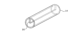
- FIG. 2 is a schematic configuration diagram of the rotary target shown in FIG.
- FIG. 3 is a schematic diagram illustrating the operation of the rotary target and the magnet of the sputtering apparatus according to the first embodiment.
- FIG. 4 is a schematic view showing the operation of the rotary target and the magnet in the film forming process according to the prior art.
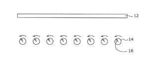
- FIG. 5 is a schematic diagram for explaining the operation of the rotary target and the magnet in the film forming process according to the first and second embodiments.
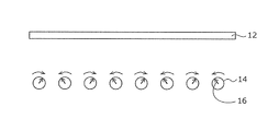
- FIG. 6 is a schematic diagram for explaining the operation of the rotary target and the magnet in the film forming process according to the first and second embodiments.
- FIG. 1 is a schematic configuration diagram of a sputtering apparatus according to the first embodiment.
- FIG. 2 is a schematic configuration diagram of the rotary target shown in FIG.
- FIG. 3 is a schematic diagram illustrating the operation of the rotary target and the
- FIG. 7 is a flowchart showing a film forming process by the sputtering apparatus according to the first embodiment.
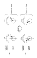
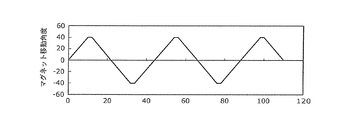
- FIG. 8A is a timing chart showing a film forming process by the sputtering apparatus according to Embodiment 1, and shows a relationship between time and a magnet angle.
- FIG. 8B is a timing chart showing a film forming process by the sputtering apparatus according to Embodiment 1, and shows a relationship between time and the rotation direction of the rotary target (cathode).
- FIG. 8C is a timing chart showing a film forming process by the sputtering apparatus according to Embodiment 1, and shows a relationship between time and ON / OFF of the DC power source.
- FIG. 1A and 1B are schematic views showing the configuration of the sputtering apparatus 1, wherein FIG. 1A is a bottom view and FIG. 1B is a front view.
- the sputtering apparatus 1 includes a substrate 12 for forming a thin film and a plurality of rotary targets 14 disposed so as to face the substrate 12 in a chamber 10.
- the sputtering apparatus 1 deposits atoms ejected from the rotary target 14 on a substrate 12 made of glass, for example, by causing Ar ions generated by plasma to collide with the rotary target 14. Thereby, a thin film can be formed on the substrate 12.
- FIG. 2 is a schematic configuration diagram of the rotary target 14 shown in FIG.
- the rotary target 14 is made of, for example, a compound semiconductor such as In or oxygen, and has a cylindrical shape with a diameter of about 160 mm and a length of about 2.7 m.
- twelve rotary targets 14 are arranged.
- the twelve rotary targets 14 are arranged in parallel to each other. Further, each rotary target 14 is arranged so that the outer side of the cylindrical shape faces the substrate 12.
- the rotary target 14 functions as a cathode in the sputtering apparatus 1.
- each of the rotary targets 14 includes a magnet 16 inside a cylindrical shape.
- the magnet 16 is disposed along the longitudinal direction of the rotary target 14 inside the cylindrical shape of the rotary target 14.
- the magnet 16 is provided in the sputtering apparatus 1 to adjust the generation position of plasma on the target.
- the rotary target 14 near the position where the magnet 16 is disposed is the rotary target 14 at the position where the magnet 16 is not disposed. Compared with, the amount of sputtering can be increased.
- the magnet 16 is indicated by an arrow.
- the tip side of the arrow is an N pole and the root side is an S pole.
- a backing tube (not shown) is disposed between the rotary target 14 and the magnet 16.
- the rotary target 14 and the magnet 16 are each provided with a gear (not shown) so as to rotate around the cylindrical axis of the rotary target 14. Thereby, the rotary target 14 and the magnet 16 can rotate separately. In other words, the plurality of magnets 16 operate independently from the rotary targets 14 arranged respectively.
- the sputtering apparatus 1 includes an exhaust device such as a dry pump and a turbo pump for exhausting the inside of the chamber 10 to a vacuum state, and a supply device for supplying a process gas in the chamber 10. And a DC power source for generating plasma.
- an exhaust device such as a dry pump and a turbo pump for exhausting the inside of the chamber 10 to a vacuum state
- a supply device for supplying a process gas in the chamber 10.
- a DC power source for generating plasma.
- FIG. 3 is a schematic view showing the operation of the rotary target 14 and the magnet 16 of the sputtering apparatus 1.
- the magnet 16 rotates around the cylindrical axis of the rotary target 14.
- the magnet 16 rotates by a predetermined angle in the CW (clockwise) direction, and rotates by a predetermined angle in the CCW (counterclockwise) direction after a predetermined period.
- the rotary target 14 rotates around the axis of the rotary target 14 at a rotation speed determined in the CW direction.
- the 12 rotary targets 14 and the magnet 16 perform the following operations.
- FIG. 4 is a schematic diagram showing the operation of the rotary target 14 and the magnet 16 in the sputtering apparatus 1 according to the prior art for comparison with the present embodiment.
- 5 and 6 are schematic diagrams for explaining the operation of the rotary target 14 and the magnet 16 in the sputtering apparatus 1 according to the present embodiment. 4 to 6, the number of rotary targets 14 and magnets 16 is omitted to be eight.
- the rotary target 14 and the magnet 16 in the conventional sputtering apparatus As shown in FIG. 4, the rotary target 14 and the magnet 16 rotate in the same direction, and the adjacent rotary target 14 rotates in the same direction. It swings at a predetermined angle. In the case of such a configuration, there arises a problem that the film thickness of the thin film formed on the substrate 12 is uneven.
- the rotary target 14 and the magnet 16 in the sputtering apparatus 1 rotate in the same direction as shown in FIG. 16 rotates in the opposite direction.
- the adjacent rotary target 14 and magnet 16 rotate in the direction opposite to the rotation direction shown in FIG.
- the rotary target 14a and the magnet 16a rotate in the CW direction.
- the rotary target 14b and the magnet 16b rotate in the CCW direction opposite to the rotary target 14a and the magnet 16a.
- the rotary target 14a and the magnet 16a rotate in the CCW direction.
- the rotary target 14b and the magnet 16b rotate in the CW direction opposite to the rotary target 14a and the magnet 16a.
- the film thickness of the thin film formed on the substrate 12 can be made uniform.
- FIG. 7 is a flowchart showing a film forming process by the sputtering apparatus 1.
- the position where the magnets 16a and 16b are closest to the substrate is defined as a rotation angle of 0 ° of the magnets 16a and 16b.
- rotation in the CW direction is defined as + direction rotation
- rotation in the CCW direction is defined as ⁇ direction rotation.
- a substrate 12 on which a thin film is to be formed is disposed at a predetermined position in the chamber 10.
- the chamber 10 is evacuated by a pump such as a cryopump and a turbo pump.
- the pressure in the chamber 10 is, for example, not more than a predetermined pressure of 0.01 Pa or less.
- argon (Ar) gas or the like is supplied into the chamber 10.
- a DC power source (not shown) is turned on, and plasma is generated in the chamber 10. That is, plasma discharge is started.
- sputtering of the rotary targets 14a and 14b is started. Adjustment may be performed so that only the rotary target 14a or only the rotary target 14b becomes a target by adjusting the power density of the rotary targets 14a and 14b of the DC power source.
- the magnet 16a is rotationally moved in the CW direction from the position where the rotation angle is 0 ° by the gear provided on the magnet 16a (step S10).
- step S11 When the magnet 16a is rotated by a predetermined angle, the rotation of the magnet 16a is stopped (step S11). For example, as shown in FIG. 8A, the magnet 16a is rotationally moved to a position of 40 ° in the CW direction, that is, a position of + 40 ° with respect to a position of a rotation angle of 0 °.
- the magnet 16b adjacent to the magnet 16a is rotationally moved in the CCW direction which is the opposite direction to the magnet 16a.
- the magnet 16b is moved relative to the position of the rotation angle 0 °. It is rotated to the position of -40 °.
- step S12 DC power is applied to the rotary targets 14a and 14b, and a thin film is formed on the substrate 12 (step S12).
- the magnet 16a is rotationally moved in the CCW direction while applying DC power (step S13).
- the rotary target 14a is rotationally moved in the same CCW direction as the magnet 16a. That is, the rotary target 14a is rotated in the forward direction with respect to the swinging direction of the magnet 16a.
- the rotation of the magnet 16a and the rotary target 14a is stopped (step S14).
- the magnet 16a is rotationally moved to a position of ⁇ 40 ° with respect to a position of 80 ° in the CCW direction, that is, a rotation angle of 0 °.
- the magnet 16a and the rotary target 14b adjacent to the magnet 16a and the rotary target 14a are rotationally moved in the CW direction, which is the opposite direction to the magnet 16a and the rotary target 14a.
- the magnet 16a when the magnet 16a is rotationally moved to the position of ⁇ 40 ° with respect to the position of the rotation angle 0 °, the magnet 16b is rotated to the position of + 40 ° with respect to the position of the rotation angle 0 °. Moved.
- step S15 application of power to the rotary targets 14a and 14b is stopped.
- step S16 while applying electric power to the rotary targets 14a and 14b again (step S16), the magnet 16a is rotationally moved in the CW direction to a position of 40 ° with respect to a rotation angle of 0 ° (step S17). At that time, the rotary target 14a is rotated in the same CW direction as the magnet 16a. When the magnet 16a is moved by a predetermined rotation, the rotation of the magnet 16a and the rotary target 14a is stopped (step S18).
- step S19 when the application of DC power is stopped (step S19) and the film thickness of the thin film formed on the substrate 12 has reached a predetermined film thickness (Yes in step S20), the film forming process is terminated. . If the thickness of the thin film formed on the substrate 12 does not reach the predetermined thickness, the magnet 16a and the rotary target 14a are rotated again in the CW direction (step S10). Similarly, the magnet 16b and the rotary target 14b are rotated and moved again in the CCW direction. Steps S10 to S20 are repeated until the thin film formed on the substrate 12 reaches a predetermined film thickness.
- the film thickness of the thin film formed on the substrate 12 is 100 nm, for example. Further, the thickness of the thin film is not limited to this, and may be several tens of nm.
- FIG. 8A to FIG. 8C are timing charts showing a film forming process by the sputtering apparatus 1.
- FIG. 8A is a diagram showing a relationship between time and a magnet angle.
- FIG. 8B is a diagram showing time and rotary target (cathode).
- FIG. 8C is a diagram showing the relationship between the rotation direction and
- FIG. 8C is a diagram showing the relationship between time and DC power ON or OFF.
- the magnet 16a and the rotary target 14a, and the magnet 16b and the rotary target 14b are rotated at a rotation angle width of 80 ° around the rotation angle of 0 °. Moved (magnet angle 80 °).
- the cycle of the film forming process described above is, for example, 20 seconds. That is, after the magnet 16a and the rotary target 14a (or the magnet 16b and the rotary target 14b) move in the CW direction in 0.5 sec, DC power is applied to the target for a period of 19.5 sec (see FIGS. 8B and 8C). Thereafter, after the magnet 16a and the rotary target 14a (or the magnet 16b and the rotary target 14b) move in the CCW direction in 0.5 sec, DC power is applied to the target for a period of 19.5 sec (FIG. 8B and FIG. 8). 8C).
- the magnets 16a and 16b are rotated and moved in the reverse direction at regular intervals, so that the rotary targets 14a and 14b are sputtered evenly and formed on the substrate 12. In-plane uniformity of the film quality of the thin film to be formed can be improved.
- an EL display device is a sputtering apparatus that forms a film on a substrate, and has a plurality of rotary targets that have a cylindrical shape and are arranged in parallel to each other. And a plurality of magnets arranged inside the cylindrical shape of each of the rotary targets, each of the plurality of magnets rotating independently of the rotary target on which the plurality of magnets are arranged.
- the magnet and the rotary target operate independently from each other, the rotary target is uniformly sputtered, and the in-plane uniformity of the film quality of the thin film formed on the substrate can be improved.
- the plurality of magnets arranged in the plurality of adjacent rotary targets may rotate in different directions.
- the adjacent magnets are rotated in the reverse direction at regular intervals, so that the rotary target is sputtered without unevenness and the in-plane uniformity of the film quality of the thin film formed on the substrate Can be improved.
- each of the plurality of rotary targets may rotate in the same direction as the magnets arranged on the plurality of rotary targets.
- the film quality of the thin film can be made more uniform by rotating the rotary target in the same direction as the magnet.
- the plurality of magnets disposed on the end side of the substrate may have a smaller rotation angle than the plurality of magnets disposed on the center side of the substrate.
- the rotation angle of the magnet becomes smaller as it is arranged on the end side of the substrate, the film quality of the thin film formed on the substrate can be further adjusted.
- Embodiment 2 Next, the sputtering apparatus concerning Embodiment 2 is demonstrated.
- the difference between the sputtering apparatus according to the present embodiment and the sputtering apparatus according to the first embodiment is that the rotation angles of a plurality of arranged magnets and rotary targets are individually set.
- the rotation angle of the magnet 16 and the rotary target 14 is, for example, the magnet 16 closest to the end portion side of the substrate 12. Further, the angle is 55 ° for the rotary target 14, 70 ° for the magnet 16 and the rotary target 14 closest to the end of the substrate 12, and 80 ° for the other magnets 16 and the rotary target 14. That is, the rotation angle of the magnet and the rotary target is reduced as the end of the substrate 12 is approached.
- the thin film formed on the substrate 12 becomes thinner as it approaches the end side of the substrate 12, but according to the configuration described above, even a thin film formed near the end of the substrate 12 is formed thin.
- the film quality of the thin film formed on the substrate 12 can be made uniform.
- the rotation angles of the magnet 16 and the rotary target 14 are set to 55 °, 70 °, and 80 ° from the side closest to the end side of the substrate 12, but the rotation of the magnet 16 and the rotary target 14 is performed.
- the angle is not limited to these and may be changed as appropriate.
- the film quality of the thin film formed on the substrate 12 can be made uniform.
- the rotation angles of the magnet 16 and the rotary target 14 are set to 55 °, 70 °, and 80 ° from the side closest to the end side of the substrate 12, but the rotation of the magnet 16 and the rotary target 14 is performed.
- the angle is not limited to these and may be changed as appropriate.
- the thickness of the thin film formed on the substrate 12 is about 100 nm.
- the thickness of the thin film is not limited to this, and may be changed as appropriate.
- the present disclosure can be used for a thin film forming apparatus for forming a semiconductor element constituting an EL display device.
Landscapes
- Chemical & Material Sciences (AREA)
- Engineering & Computer Science (AREA)
- Physics & Mathematics (AREA)
- Plasma & Fusion (AREA)
- Analytical Chemistry (AREA)
- Chemical Kinetics & Catalysis (AREA)
- Materials Engineering (AREA)
- Mechanical Engineering (AREA)
- Metallurgy (AREA)
- Organic Chemistry (AREA)
- Physical Vapour Deposition (AREA)
Abstract
スパッタリング装置(1)であって、筒型の形状を有し、互いに平行に配置された複数のロータリーターゲット(14aおよび14b)と、複数のロータリーターゲット(14aおよび14b)のそれぞれの筒型の形状の内部に配置された、複数のマグネット(16aおよび16b)とを備え、複数のマグネット(16aおよび16b)のそれぞれは、各複数のマグネット(16aおよび16b)が配置されたロータリーターゲット(14aおよび14b)と独立に回転する。
Description
本開示は、基板上に薄膜を形成するためのスパッタリング装置に関する。
特許文献1は、筒型のターゲットを円筒軸の周りに回転させながら放電を行うスパッタターゲットを用いたスパッタリング装置について開示されている。
このスパッタリング装置は、チャンバ内に、筒型に形成されたロータリーターゲットを備えている。ロータリーターゲットの筒型の形状の内部には、ロータリーターゲットの長尺方向に長尺なマグネットが設けられている。このスパッタリング装置は、チャンバ内にガスを導入してロータリーターゲットを回転しながら放電させることにより、ロータリーターゲットに対向して配置された基板上に薄膜を形成するものである。
この構成によれば、筒状のターゲットが均一にエロージョン(浸食)されるため、ターゲットの利用効率が高いという利点がある。
一方、特許文献1に記載されたスパッタリング装置では、チャンバ内の水又は残留ガス等によってターゲット表面が酸化する、または、ターゲット表面に変質層が形成されることがある。したがって、基板上に成膜された薄膜の膜質を、例えば、マイクロ波検出型光導電減衰法によって評価した場合、膜質の面内均一性に悪影響を及ぼすおそれがある。
上記課題に鑑み、本開示は、成膜される薄膜の膜質の面内均一性を向上するスパッタリング装置を提供することを目的とする。
本開示の一態様に係るスパッタリング装置は、基板に成膜するスパッタリング装置であって、筒型の形状を有し、互いに平行に配置された複数のロータリーターゲットと、前記複数のロータリーターゲットそれぞれの筒型の形状の内部に配置された、複数のマグネットとを備え、前記複数のマグネットのそれぞれは、各前記複数のマグネットが配置された前記ロータリーターゲットと独立に回転する。
本開示によれば、成膜される薄膜の膜質の面内均一性を向上するスパッタリング装置を提供することができる。
以下、適宜図面を参照しながら、実施の形態を詳細に説明する。但し、必要以上に詳細な説明は省略する場合がある。例えば、既によく知られた事項の詳細説明や実質的に同一の構成に対する重複説明を省略する場合がある。これは、以下の説明が不必要に冗長になるのを避け、当業者の理解を容易にするためである。
なお、発明者らは、当業者が本開示を十分に理解するために添付図面および以下の説明を提供するものであって、これらによって請求の範囲に記載の主題を限定することを意図するものではない。
(実施の形態1)
以下、図1~図8Cを用いて、本開示の実施の形態に係るスパッタリング装置1について説明する。
以下、図1~図8Cを用いて、本開示の実施の形態に係るスパッタリング装置1について説明する。
[スパッタリング装置の構成]
図1は、スパッタリング装置1の構成を示す概略図であり、(a)は下面図、(b)は正面図である。
図1は、スパッタリング装置1の構成を示す概略図であり、(a)は下面図、(b)は正面図である。
図1に示すように、スパッタリング装置1は、チャンバ10内に、薄膜を形成するための基板12と、基板12と対向するように配置された複数のロータリーターゲット14とを備えている。
スパッタリング装置1は、プラズマにより発生したArイオンをロータリーターゲット14に衝突させることによりロータリーターゲット14から弾き出された原子を、例えばガラスで構成される基板12に堆積する。これにより、基板12の上に薄膜を形成することができる。
図2は、図1に示したロータリーターゲット14の概略構成図である。
図2に示すように、ロータリーターゲット14は、例えば、化合物半導体であるIn、酸素などで構成され、直径160mm程度、長さが2.7m程度の筒型の形状を有している。ロータリーターゲット14は、たとえば12本配置されている。12本のロータリーターゲット14は、互いに平行に配置されている。また、各ロータリーターゲット14は、筒型の形状の外側が基板12と対向するように配置されている。ロータリーターゲット14は、スパッタリング装置1においてカソードとして機能する。
また、ロータリーターゲット14のそれぞれは、筒型の形状の内部に、マグネット16を備えている。
マグネット16は、ロータリーターゲット14の筒型の形状の内側に、ロータリーターゲット14の長尺方向に沿って配置されている。マグネット16は、スパッタリング装置1において、ターゲット上でのプラズマの発生位置を調整するために設けられている。
詳細には、スパッタリング装置1において、マグネット16の近傍にはArイオンが多く存在するため、マグネット16が配置された位置近傍のロータリーターゲット14は、マグネット16が配置されていない位置でのロータリーターゲット14と比較して、スパッタリング量を増加することができる。
なお、図1において、マグネット16は矢印で示しているが、例えば矢印の先端側をN極、根元側をS極とする。
また、ロータリーターゲット14とマグネット16との間には、バッキングチューブ(図示せず)が配置されている。ロータリーターゲット14とマグネット16とは、ロータリーターゲット14の円筒軸を中心に回転動作をするように、それぞれギア(図示せず)が設けられている。これにより、ロータリーターゲット14とマグネット16とは、別々に回転動作をすることができる。すなわち、複数のマグネット16は、それぞれ配置されたロータリーターゲット14から独立して動作する。
さらに、図示を省略するが、スパッタリング装置1は、チャンバ10内を真空状態まで排気するためのドライポンプおよびターボポンプ等の排気装置と、チャンバ10内にあるプロセスガスを供給するための供給装置と、プラズマを発生させるためのDC電源等とを備えている。
[スパッタリング装置の動作]
ここで、スパッタリング装置1の動作について、図3~図8Cを用いて説明する。
ここで、スパッタリング装置1の動作について、図3~図8Cを用いて説明する。
図3は、スパッタリング装置1のロータリーターゲット14およびマグネット16の動作を示す概略図である。
図3に示すように、マグネット16は、ロータリーターゲット14の円筒軸を中心として回転動作をする。マグネット16は、CW(Clockwise:時計周り)方向に所定角度回転し、所定期間経過後にCCW(Counterclockwise:反時計回り)方向に所定角度回転する。
このとき、ロータリーターゲット14は、ロータリーターゲット14の軸を中心として、CW方向に定められた回転数で回転する。
スパッタリング装置1においては、12本のロータリーターゲット14およびマグネット16は、以下のような動作を行う。
図4は、本実施の形態との比較のための、従来技術に係るスパッタリング装置1におけるロータリーターゲット14及びマグネット16の動作を示す概略図である。図5および図6は、本実施の形態に係るスパッタリング装置1におけるロータリーターゲット14およびマグネット16の動作を説明するための概略図である。なお、図4~図6では、ロータリーターゲット14およびマグネット16の数を8本に省略して示している。
従来のスパッタリング装置におけるロータリーターゲット14およびマグネット16では、図4に示すように、ロータリーターゲット14およびマグネット16が同一方向に回転し、かつ、隣接するロータリーターゲット14が同一方向に回転し、マグネット16が定められた角度で揺動運動するものである。このような構成の場合、基板12の上に形成された薄膜の膜厚にムラが生じるという問題が生じる。
これに対し、本実施の形態に係るスパッタリング装置1におけるロータリーターゲット14およびマグネット16では、図5に示すように、ロータリーターゲット14およびマグネット16は同一方向に回転するが、隣接するロータリーターゲット14およびマグネット16は、逆方向に回転する。また、図5に示す状態で所定の期間が経過した後、図6に示すように、隣接するロータリーターゲット14およびマグネット16は、それぞれ図5に示した回転方向と逆方向に回転する。
例えば、図5に示すように、ロータリーターゲット14aおよびマグネット16aは、CW方向に回転する。このとき、ロータリーターゲット14bおよびマグネット16bは、ロータリーターゲット14aおよびマグネット16aと逆方向のCCW方向に回転する。
所定の期間が経過した後、図6に示すように、ロータリーターゲット14aおよびマグネット16aは、CCW方向に回転する。このとき、ロータリーターゲット14bおよびマグネット16bは、ロータリーターゲット14aおよびマグネット16aと逆方向のCW方向に回転する。
このような動作とすることにより、基板12の上に形成される薄膜の膜厚を均一にすることができる。
次に、スパッタリング装置1を用いた成膜の工程について説明する。
図7は、スパッタリング装置1による成膜の工程を示すフローチャートである。なお、基板に対してマグネット16aおよび16bが最も近接した位置を、マグネット16aおよび16bの回転角度0°とする。また、CW方向の回転を+方向の回転、CCW方向の回転を-方向の回転とする。
成膜の工程の前段階として、はじめに、チャンバ10内の所定の位置に、薄膜を形成しようとする基板12が配置される。その後、例えばクライオポンプおよびターボポンプなどのポンプにより、チャンバ10内の排気が行われる。チャンバ10内の圧力は、例えば0.01Pa以下の定められた圧力以下とする。チャンバ10内が前述の真空度となるまでチャンバ10内の排気が行われた後、チャンバ10内にはアルゴン(Ar)ガスなどが供給される。
その後、DC電源(図示せず)がON状態にされ、チャンバ10内にプラズマが発生する。すなわち、プラズマ放電が開始される。
チャンバ10内においてプラズマ放電が開始されると、ロータリーターゲット14aおよび14bのスパッタリングが開始される。なお、DC電源のロータリーターゲット14aおよび14bに対する電力密度を調整することにより、ロータリーターゲット14aのみ、又は、ロータリーターゲット14bのみがターゲットとなるように調整が行われてもよい。
そして、図7に示すように、マグネット16aに設けられたギアにより、マグネット16aが回転角度0°の位置からCW方向に回転移動される(ステップS10)。
マグネット16aが所定の角度回転移動されたところで、マグネット16aの回転が停止される(ステップS11)。マグネット16aは、例えば、図8Aに示すように、CW方向へ40°、すなわち、回転角度0°の位置に対して+40°の位置まで回転移動される。
このとき、マグネット16aと隣接するマグネット16bは、マグネット16aと逆方向であるCCW方向に回転移動される。例えば、図8Aに示すように、上記したようにマグネット16aが回転角度0°の位置に対して+40°の位置まで回転移動される場合には、マグネット16bは回転角度0°の位置に対して-40°の位置まで回転移動される。
その後、ロータリーターゲット14aおよび14bにDC電力が印加され、基板12上に薄膜が形成される(ステップS12)。
さらに、DC電力を印加しながら、マグネット16aがCCW方向に回転移動される(ステップS13)。このとき、ロータリーターゲット14aは、マグネット16aと同一のCCW方向に回転移動される。すなわち、ロータリーターゲット14aは、マグネット16aの揺動方向に対して順方向に回転される。
マグネット16aが所定の角度回転移動されたところで、マグネット16aおよびロータリーターゲット14aの回転は停止される(ステップS14)。マグネット16aは、例えば、CCW方向へ80°、すなわち、回転角度0°の位置に対して-40°の位置まで回転移動される。このとき、マグネット16aおよびロータリーターゲット14aと隣接するマグネット16bおよびロータリーターゲット14bは、マグネット16aおよびロータリーターゲット14aと逆方向であるCW方向に回転移動される。例えば、上記したようにマグネット16aが回転角度0°の位置に対して-40°の位置まで回転移動される場合には、マグネット16bは回転角度0°の位置に対して+40°の位置まで回転移動される。
その後、ロータリーターゲット14aおよび14bへの電力の印加が停止される(ステップS15)。
次に、再びロータリーターゲット14aおよび14bに電力を印加しながら(ステップS16)、マグネット16aは回転角度0°に対して40°の位置までCW方向で回転移動される(ステップS17)。そのときロータリーターゲット14aは、マグネット16aと同一のCW方向に回転される。マグネット16aが所定の回転移動されたところでマグネット16aおよびロータリーターゲット14aの回転は停止される(ステップS18)。
その後、ロータリーターゲット14aおよび14bにDC電力の印加が停止され、基板12上に薄膜が形成される。
さらに、DC電力の印加が停止され(ステップS19)、基板12上に形成された薄膜の膜厚が所定の膜厚に達していれば(ステップS20においてYes)、成膜の工程は終了される。また、基板12上に形成された薄膜の膜厚が所定の膜厚に達していなければ、マグネット16aおよびロータリーターゲット14aは再びCW方向に回転移動される(ステップS10)。同様に、マグネット16bおよびロータリーターゲット14bは再びCCW方向に回転移動される。そして、基板12上に形成された薄膜が所定の膜厚に達するまで、上記ステップS10~ステップS20が繰り返される。
なお、基板12上に形成される薄膜の膜厚は、例えば、100nmである。また、薄膜の膜厚はこれに限られず、数十nmであってもよい。
図8A~図8Cは、スパッタリング装置1による成膜の工程を示すタイミングチャートであり、図8Aは、時間とマグネット角度との関係を示した図、図8Bは、時間とロータリーターゲット(カソード)の回転方向との関係を示した図、図8Cは、時間とDC電源のONまたはOFFとの関係を示した図である。
上記した成膜の工程では、図8Aに示すように、マグネット16aおよびロータリーターゲット14aと、マグネット16bおよびロータリーターゲット14bとは、回転角度0°の位置を中心に80°の回転角度の幅で回転移動される(マグネット角度 80°)。
また、上記した成膜の工程の周期は、例えば20secである。すなわち、マグネット16aおよびロータリーターゲット14a(または、マグネット16bおよびロータリーターゲット14b)はCW方向に0.5secで移動した後、19.5secの期間ターゲットにDC電力が印加され(図8Bおよび図8C参照)、その後、マグネット16aおよびロータリーターゲット14a(または、マグネット16bおよびロータリーターゲット14b)はCCW方向に0.5secで移動した後、19.5secの期間ターゲットにDC電力の印加が行われる(図8Bおよび図8C参照)。
以上、本実施の形態に係るスパッタリング装置1によれば、マグネット16aおよび16bが一定の周期ごとに逆方向に回転移動されるので、ロータリーターゲット14aおよび14bはムラなくスパッタリングされ、基板12上に成膜される薄膜の膜質の面内均一性を向上することができる。
[効果等]
以上のように、本開示の一態様に係るEL表示装置は、基板に成膜するスパッタリング装置であって、筒型の形状を有し、互いに平行に配置された複数のロータリーターゲットと、前記複数のロータリーターゲットそれぞれの筒型の形状の内部に配置された、複数のマグネットとを備え、前記複数のマグネットのそれぞれは、各前記複数のマグネットが配置された前記ロータリーターゲットと独立に回転する。
以上のように、本開示の一態様に係るEL表示装置は、基板に成膜するスパッタリング装置であって、筒型の形状を有し、互いに平行に配置された複数のロータリーターゲットと、前記複数のロータリーターゲットそれぞれの筒型の形状の内部に配置された、複数のマグネットとを備え、前記複数のマグネットのそれぞれは、各前記複数のマグネットが配置された前記ロータリーターゲットと独立に回転する。
この構成によれば、マグネットとロータリーターゲットとは、それぞれ独立して動作するため、ロータリーターゲットはムラなくスパッタリングされ、基板上に成膜される薄膜の膜質の面内均一性を向上することができる。
また、隣接する前記複数のロータリーターゲットに配置された前記複数のマグネットは、互いに異なる方向に回転するとしてもよい。
この構成によれば、隣接する複数のマグネットは、一定の周期ごとに逆方向に回転移動されるので、ロータリーターゲットはムラなくスパッタリングされ、基板上に成膜される薄膜の膜質の面内均一性を向上することができる。
また、前記複数のロータリーターゲットのそれぞれは、前記複数のロータリーターゲットに配置された前記マグネットと同一の方向に回転するとしてもよい。
この構成によれば、ロータリーターゲットがマグネットと同一方向に回転することにより、薄膜の膜質をより均一にすることができる。
また、前記基板の端部側に配置された前記複数のマグネットは、前記基板の中央側に配置された前記複数のマグネットより回転角度が小さいとしてもよい。
この構成によれば、基板の端部側に配置されるほどマグネットの回転角度が小さくなるため、基板上に形成される薄膜の膜質をより調整することができる。
(実施の形態2)
次に、実施の形態2にかかるスパッタリング装置について説明する。
次に、実施の形態2にかかるスパッタリング装置について説明する。
本実施の形態に係るスパッタリング装置が実施の形態1に係るスパッタリング装置と異なる点は、複数配置されたマグネットおよびロータリーターゲットの回転角度が個々に設定される点である。
図5及び図6に示したマグネット16およびロータリーターゲット14を用いて説明すると、本実施の形態に係るマグネット16およびロータリーターゲット14の回転角度は、例えば、基板12の端部側に最も近いマグネット16およびロータリーターゲット14では55°、基板12の端部側に2番目に近いマグネット16およびロータリーターゲット14では70°、その他のマグネット16およびロータリーターゲット14では80°とする。すなわち、基板12の端部側に近づくに連れてマグネットおよびロータリーターゲットの回転角度を小さくする。
一般的に、基板12上に形成された薄膜は、基板12の端部側に近づくにつれて薄くなるが、前述した構成によると、基板12の端部付近に形成される薄膜であっても薄く形成されることはなく、基板12上に形成される薄膜の膜質を均一にすることができる。
なお、前述した構成では、マグネット16およびロータリーターゲット14の回転角度を、基板12の端部側に最も近いほうから55°、70°、80°と設定したが、マグネット16およびロータリーターゲット14の回転角度はこれらに限定されるものではなく、適宜変更してもよい。
(他の実施の形態)
以上のように、本出願において開示する技術の例示として、実施の形態を説明した。しかしながら、本開示における技術は、これに限定されず、適宜、変更、置き換え、付加、省略などを行った実施の形態にも適用可能である。また、上記実施の形態で説明した各構成要素を組み合わせて、新たな実施の形態とすることも可能である。
以上のように、本出願において開示する技術の例示として、実施の形態を説明した。しかしながら、本開示における技術は、これに限定されず、適宜、変更、置き換え、付加、省略などを行った実施の形態にも適用可能である。また、上記実施の形態で説明した各構成要素を組み合わせて、新たな実施の形態とすることも可能である。
そこで、以下、他の実施の形態をまとめて説明する。
例えば、前述した実施の形態に係るスパッタリング装置では、基板12上に形成される薄膜の膜質を均一にすることができる。
なお、前述した構成では、マグネット16およびロータリーターゲット14の回転角度を、基板12の端部側に最も近いほうから55°、70°、80°と設定したが、マグネット16およびロータリーターゲット14の回転角度はこれらに限定されるものではなく、適宜変更してもよい。
また、前述したスパッタリング装置では、基板12上に形成される薄膜の膜厚は100nm程度としたが、薄膜の膜厚はこれに限定されず、適宜変更してもよい。
以上のように、本開示における技術の例示として、実施の形態を説明した。そのために、添付図面および詳細な説明を提供した。
したがって、添付図面および詳細な説明に記載された構成要素の中には、課題解決のために必須な構成要素だけでなく、上記技術を例示するために、課題解決のためには必須でない構成要素も含まれ得る。そのため、それらの必須ではない構成要素が添付図面や詳細な説明に記載されていることをもって、直ちに、それらの必須ではない構成要素が必須であるとの認定をするべきではない。
また、上述の実施の形態は、本開示における技術を例示するためのものであるから、請求の範囲またはその均等の範囲において種々の変更、置き換え、付加、省略などを行うことができる。
本開示は、EL表示装置を構成する半導体素子を形成するための薄膜の形成装置に利用することができる。
1 スパッタリング装置
10 チャンバ
12 基板
14、14a、14b ロータリーターゲット
16、16a、16b マグネット
10 チャンバ
12 基板
14、14a、14b ロータリーターゲット
16、16a、16b マグネット
Claims (4)
- 基板に成膜するスパッタリング装置であって、
筒型の形状を有し、互いに平行に配置された複数のロータリーターゲットと、
前記複数のロータリーターゲットそれぞれの筒型の形状の内部に配置された、複数のマグネットとを備え、
前記複数のマグネットのそれぞれは、各前記複数のマグネットが配置された前記ロータリーターゲットと独立に回転する
スパッタリング装置。 - 隣接する前記複数のロータリーターゲットに配置された前記複数のマグネットは、互いに異なる方向に回転する
請求項1に記載のスパッタリング装置。 - 前記複数のロータリーターゲットのそれぞれは、前記複数のロータリーターゲットに配置された前記マグネットと同一の方向に回転する
請求項1または2に記載のスパッタリング装置。 - 前記基板の端部側に配置された前記複数のマグネットは、前記基板の中央側に配置された前記複数のマグネットより回転角度が小さい
請求項1~3のいずれか1項に記載のスパッタリング装置。
Applications Claiming Priority (2)
| Application Number | Priority Date | Filing Date | Title |
|---|---|---|---|
| JP2013235840 | 2013-11-14 | ||
| JP2013-235840 | 2013-11-14 |
Publications (1)
| Publication Number | Publication Date |
|---|---|
| WO2015072046A1 true WO2015072046A1 (ja) | 2015-05-21 |
Family
ID=53057004
Family Applications (1)
| Application Number | Title | Priority Date | Filing Date |
|---|---|---|---|
| PCT/JP2014/003392 Ceased WO2015072046A1 (ja) | 2013-11-14 | 2014-06-24 | スパッタリング装置 |
Country Status (1)
| Country | Link |
|---|---|
| WO (1) | WO2015072046A1 (ja) |
Cited By (5)
| Publication number | Priority date | Publication date | Assignee | Title |
|---|---|---|---|---|
| CN109750267A (zh) * | 2019-03-26 | 2019-05-14 | 合肥京东方显示技术有限公司 | 一种磁控溅射装置 |
| JP2019519673A (ja) * | 2016-04-21 | 2019-07-11 | アプライド マテリアルズ インコーポレイテッドApplied Materials,Incorporated | 基板をコーティングするための方法、及びコータ |
| WO2021028010A1 (en) * | 2019-08-09 | 2021-02-18 | Applied Materials, Inc. | Method of coating a substrate and coating apparatus for coating a substrate |
| CN114981470A (zh) * | 2020-07-08 | 2022-08-30 | 株式会社爱发科 | 成膜方法 |
| JP2023033718A (ja) * | 2021-08-30 | 2023-03-13 | 株式会社アルバック | 成膜方法及び成膜装置 |
Citations (5)
| Publication number | Priority date | Publication date | Assignee | Title |
|---|---|---|---|---|
| JPH0688229A (ja) * | 1991-01-29 | 1994-03-29 | Boc Group Inc:The | 二重円筒マグネトロンに於けるスパッタリングターゲットの磁場ゾーン回転の電気制御 |
| JP2002529600A (ja) * | 1998-11-06 | 2002-09-10 | シヴァク | 高レート・コーティング用のスパッタリング装置および方法 |
| JP2005350768A (ja) * | 2004-05-05 | 2005-12-22 | Applied Films Gmbh & Co Kg | 回転可能なマグネトロンの大面積アセンブリを有するコーター |
| US20130032476A1 (en) * | 2011-08-04 | 2013-02-07 | Sputtering Components, Inc. | Rotary cathodes for magnetron sputtering system |
| JP2013506756A (ja) * | 2009-10-02 | 2013-02-28 | アプライド マテリアルズ インコーポレイテッド | 基板をコーティングするための方法およびコータ |
-
2014
- 2014-06-24 WO PCT/JP2014/003392 patent/WO2015072046A1/ja not_active Ceased
Patent Citations (5)
| Publication number | Priority date | Publication date | Assignee | Title |
|---|---|---|---|---|
| JPH0688229A (ja) * | 1991-01-29 | 1994-03-29 | Boc Group Inc:The | 二重円筒マグネトロンに於けるスパッタリングターゲットの磁場ゾーン回転の電気制御 |
| JP2002529600A (ja) * | 1998-11-06 | 2002-09-10 | シヴァク | 高レート・コーティング用のスパッタリング装置および方法 |
| JP2005350768A (ja) * | 2004-05-05 | 2005-12-22 | Applied Films Gmbh & Co Kg | 回転可能なマグネトロンの大面積アセンブリを有するコーター |
| JP2013506756A (ja) * | 2009-10-02 | 2013-02-28 | アプライド マテリアルズ インコーポレイテッド | 基板をコーティングするための方法およびコータ |
| US20130032476A1 (en) * | 2011-08-04 | 2013-02-07 | Sputtering Components, Inc. | Rotary cathodes for magnetron sputtering system |
Cited By (7)
| Publication number | Priority date | Publication date | Assignee | Title |
|---|---|---|---|---|
| JP2019519673A (ja) * | 2016-04-21 | 2019-07-11 | アプライド マテリアルズ インコーポレイテッドApplied Materials,Incorporated | 基板をコーティングするための方法、及びコータ |
| CN109750267A (zh) * | 2019-03-26 | 2019-05-14 | 合肥京东方显示技术有限公司 | 一种磁控溅射装置 |
| CN109750267B (zh) * | 2019-03-26 | 2021-10-26 | 合肥京东方显示技术有限公司 | 一种磁控溅射装置 |
| WO2021028010A1 (en) * | 2019-08-09 | 2021-02-18 | Applied Materials, Inc. | Method of coating a substrate and coating apparatus for coating a substrate |
| CN114981470A (zh) * | 2020-07-08 | 2022-08-30 | 株式会社爱发科 | 成膜方法 |
| JP2023033718A (ja) * | 2021-08-30 | 2023-03-13 | 株式会社アルバック | 成膜方法及び成膜装置 |
| JP7672921B2 (ja) | 2021-08-30 | 2025-05-08 | 株式会社アルバック | 成膜方法及び成膜装置 |
Similar Documents
| Publication | Publication Date | Title |
|---|---|---|
| JP5993974B2 (ja) | 基板をコーティングするための方法およびコータ | |
| CN105102671B (zh) | Hipims溅射的方法和hipims溅射系统 | |
| WO2015072046A1 (ja) | スパッタリング装置 | |
| JP5934208B2 (ja) | 抵抗率と不均一性が減少された薄膜を形成する物理蒸着処理のためのマグネット | |
| JP2011149104A5 (ja) | ||
| JP2009024230A (ja) | スパッタリング装置 | |
| TWI652365B (zh) | 塗佈一基板之方法及用以塗佈一基板之塗佈設備 | |
| WO2013179544A1 (ja) | マグネトロンスパッタ装置 | |
| JP2004156122A (ja) | 成膜方法及びスパッタ装置 | |
| JP2022179487A (ja) | 成膜装置及び電子デバイスの製造方法 | |
| JP2019094533A (ja) | スパッタリング装置 | |
| JP6641472B2 (ja) | 成膜方法及びスパッタリング装置 | |
| JP4246546B2 (ja) | スパッタ源、スパッタリング装置、及びスパッタリング方法 | |
| WO2015025823A1 (ja) | スパッタリング成膜装置及びスパッタリング成膜方法 | |
| CN114207181B (zh) | 涂覆基板的方法、制造显示器的方法和涂覆基板的涂覆设备 | |
| JP2010095735A (ja) | 成膜装置、成膜方法およびガスバリアフィルム | |
| JP2007119829A (ja) | スパッタ成膜装置 | |
| US9558921B2 (en) | Magnetron sputtering apparatus | |
| JP5524290B2 (ja) | スパッタリング装置 | |
| KR102446178B1 (ko) | 스퍼터링 장치 | |
| JP2006176862A (ja) | スパッタ成膜装置およびスパッタ成膜方法 | |
| TWM483280U (zh) | 真空鍍膜設備的旋轉靶材裝置 | |
| JP2005054251A (ja) | スパッタリング方法 | |
| JP2013185158A (ja) | 成膜方法 | |
| JPH09202970A (ja) | 磁性薄膜の両面同時成膜装置及び両面同時成膜方法 |
Legal Events
| Date | Code | Title | Description |
|---|---|---|---|
| 121 | Ep: the epo has been informed by wipo that ep was designated in this application |
Ref document number: 14862859 Country of ref document: EP Kind code of ref document: A1 |
|
| NENP | Non-entry into the national phase |
Ref country code: DE |
|
| 122 | Ep: pct application non-entry in european phase |
Ref document number: 14862859 Country of ref document: EP Kind code of ref document: A1 |
|
| NENP | Non-entry into the national phase |
Ref country code: JP |