WO2015068439A1 - 電極体 - Google Patents
電極体 Download PDFInfo
- Publication number
- WO2015068439A1 WO2015068439A1 PCT/JP2014/070518 JP2014070518W WO2015068439A1 WO 2015068439 A1 WO2015068439 A1 WO 2015068439A1 JP 2014070518 W JP2014070518 W JP 2014070518W WO 2015068439 A1 WO2015068439 A1 WO 2015068439A1
- Authority
- WO
- WIPO (PCT)
- Prior art keywords
- film
- electrode
- barrier metal
- bonding
- temperature detection
- Prior art date
- Legal status (The legal status is an assumption and is not a legal conclusion. Google has not performed a legal analysis and makes no representation as to the accuracy of the status listed.)
- Ceased
Links
Images

Classifications
-
- H—ELECTRICITY
- H10—SEMICONDUCTOR DEVICES; ELECTRIC SOLID-STATE DEVICES NOT OTHERWISE PROVIDED FOR
- H10W—GENERIC PACKAGES, INTERCONNECTIONS, CONNECTORS OR OTHER CONSTRUCTIONAL DETAILS OF DEVICES COVERED BY CLASS H10
- H10W72/00—Interconnections or connectors in packages
- H10W72/90—Bond pads, in general
-
- H—ELECTRICITY
- H10—SEMICONDUCTOR DEVICES; ELECTRIC SOLID-STATE DEVICES NOT OTHERWISE PROVIDED FOR
- H10D—INORGANIC ELECTRIC SEMICONDUCTOR DEVICES
- H10D64/00—Electrodes of devices having potential barriers
- H10D64/20—Electrodes characterised by their shapes, relative sizes or dispositions
-
- H—ELECTRICITY
- H10—SEMICONDUCTOR DEVICES; ELECTRIC SOLID-STATE DEVICES NOT OTHERWISE PROVIDED FOR
- H10W—GENERIC PACKAGES, INTERCONNECTIONS, CONNECTORS OR OTHER CONSTRUCTIONAL DETAILS OF DEVICES COVERED BY CLASS H10
- H10W72/00—Interconnections or connectors in packages
- H10W72/50—Bond wires
- H10W72/551—Materials of bond wires
- H10W72/552—Materials of bond wires comprising metals or metalloids, e.g. silver
- H10W72/5524—Materials of bond wires comprising metals or metalloids, e.g. silver comprising aluminium [Al]
-
- H—ELECTRICITY
- H10—SEMICONDUCTOR DEVICES; ELECTRIC SOLID-STATE DEVICES NOT OTHERWISE PROVIDED FOR
- H10W—GENERIC PACKAGES, INTERCONNECTIONS, CONNECTORS OR OTHER CONSTRUCTIONAL DETAILS OF DEVICES COVERED BY CLASS H10
- H10W72/00—Interconnections or connectors in packages
- H10W72/50—Bond wires
- H10W72/59—Bond pads specially adapted therefor
Definitions
- the technique disclosed in this specification relates to an electrode body in a semiconductor device.
- Patent Document 1 discloses an electrode body of a semiconductor device.
- the electrode body of Patent Document 1 Japanese Unexamined Patent Publication No. Hei 8-203952
- the electrode body of Patent Document 1 includes an electrode film and a barrier metal film disposed under the electrode film. Wires for inputting and outputting signals are bonded to the electrode film.
- the electrode body is disposed on the substrate.
- an object of the present specification is to provide an electrode body for wire bonding with higher reliability.
- An electrode body in a semiconductor device disclosed in this specification includes an electrode film including aluminum, a barrier metal film including titanium disposed under the electrode film, and silicon disposed under the barrier metal film. And a bonding film.
- the film thickness t1 of the electrode film and the film thickness t2 of the barrier metal film satisfy the relational expression of t1 ⁇ 6.67 ⁇ t2 + 3500.
- the above film thicknesses t1 and t2 are values expressed in units of nm.
- the electrode film even when wire bonding is performed on the electrode film, for example, the electrode film is not broken or peeled off, and the quality of the electrode body can be maintained. Thereby, even if wire bonding is performed on the electrode film, it is possible to ensure the bonding reliability between the electrode body and the substrate disposed below the electrode body.
- the barrier metal film may include a titanium film that contacts the bonding film.
- a semiconductor device disclosed in this specification includes a plurality of emitter electrodes arranged side by side, a plurality of signal electrodes arranged adjacent to the emitter electrode, and the emitter electrode and the emitter electrode.
- the signal electrode and the temperature detection electrode are composed of the electrode body described above.
- the film thickness t31 of the bonding film in the signal electrode and the film thickness t32 of the bonding film in the temperature detection electrode are the same film thickness.
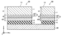
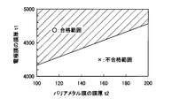
- FIG. 2 is a cross-sectional view taken along the line II-II in FIG. 1 (a cross-sectional view of an electrode body according to an embodiment). It is a graph which shows the relationship between the film thickness of an electrode film, and the film thickness of a barrier metal film.
- the semiconductor device 10 includes a plurality of signal electrodes 30, a plurality of temperature detection electrodes 50, and a plurality of emitter electrodes 40 formed on the surface of the substrate 20.
- the signal electrode 30, the temperature detection electrode 50, and the emitter electrode 40 are separated from each other.
- An example of the semiconductor device 10 is an IGBT (Insulated Gate Bipolar Transistor) including an emitter electrode, a collector electrode, and a gate electrode.
- IGBT Insulated Gate Bipolar Transistor
- FIG. 1 a plan view of the IGBT viewed from the emitter electrode 40 side is shown.
- the emitter electrode 40 is joined to an external terminal (not shown) by solder.
- the emitter electrode 40 is an electrode for solder bonding.
- the semiconductor device 10 can be formed using a method such as photolithography, etching, CVD, PVD, or the like.
- the plurality of emitter electrodes 40 are arranged side by side in the horizontal direction (x direction) in plan view.
- the substrate 20 is formed to have a substantially rectangular shape in plan view.
- the substrate 20 is made of silicon (Si).
- the substrate 20 can be formed of SiC, GaN, or the like.
- the signal electrode 30 is disposed adjacent to the emitter electrode 40.
- the plurality of signal electrodes 30 are arranged side by side in the horizontal direction (x direction) in plan view.
- the signal electrode 30 and the temperature detection electrode 50 are disposed at positions facing different side surfaces of the emitter electrode 40, respectively.
- the signal electrode 30 is disposed at a position facing the side surface in the horizontal direction (x direction) of the emitter electrode 40.
- an electrode for inputting a gate signal, an electrode for extracting a signal for detecting a current flowing through the semiconductor device 10, and a signal for detecting the temperature of the semiconductor device 10 are extracted. Electrodes.
- the temperature detection electrode 50 is disposed between the emitter electrode 40 and the emitter electrode 40 arranged in the horizontal direction.
- the plurality of temperature detection electrodes 50 are arranged side by side in the vertical direction (y direction) in plan view.
- the temperature detection electrode 50 is disposed at a position facing the side surface in the longitudinal direction (y direction) of the emitter electrode 40.
- the temperature detection electrode 50 is disposed to detect the temperature of the semiconductor device 1.
- the electrode body of the signal electrode 30 and the electrode body of the temperature detection electrode 50 will be described. Since the electrode body of the signal electrode 30 and the electrode body of the temperature detection electrode 50 in this embodiment have the same laminated structure, they will be described together. As shown in FIG. 2, the electrode bodies (signal electrode 30 and temperature detection electrode 50) are each provided with an insulating film 4 disposed on the substrate 20, and a bonding film 3 disposed on the insulating film 4. And a barrier metal film 2 disposed on the bonding film 3 and an electrode film 1 disposed on the barrier metal film 2. The electrode body of the signal electrode 30 and the electrode body of the temperature detection electrode 50 are separated from each other. The periphery of the electrode body is filled with sealing resin (not shown), and the whole is sealed.
- the electrode film 1 and the barrier metal film 2 are films mainly composed of metal.
- the electrode film 1 contains aluminum (Al) as a main component.
- an aluminum silicon alloy (AlSi) is used as the material of the electrode film 1.
- An aluminum silicon alloy is an alloy containing aluminum (Al) as a main component and added with silicon (Si).
- the surface 11 of the electrode film 1 is exposed to the outside.
- a wire (not shown) for inputting or outputting a signal is bonded to the surface 11 of the electrode film 1.
- the film thickness t1 of the electrode film 1 is set to 4.5 ⁇ m (4500 nm) or more.
- the barrier metal film 2 is disposed under the electrode film 1.
- the barrier metal film 2 contains titanium (Ti).
- the barrier metal film 2 of this embodiment has a two-layer structure, and includes a titanium film 21 disposed on the bonding film 3 and a titanium nitride film 22 disposed on the titanium film 21. .
- the titanium film 21 contains titanium (Ti) as a main component, and the titanium nitride film 22 contains titanium nitride (TiN) as a main component.
- the titanium film 21 is disposed on the lower side, and the titanium nitride film 22 is disposed on the upper side.
- the titanium film 21 is in contact with the bonding film 3 disposed therebelow.
- the titanium film 21 and the bonding film 3 are combined to form an alloy film.
- the barrier metal film 2 is a film that prevents aluminum (Al) contained in the electrode film 1 from diffusing downward from the barrier metal film 2.
- the thickness t2 of the barrier metal film 2 is 150 nm.
- the film thickness t1 (unit: nm) of the electrode film 1 and the film thickness t2 (unit: nm) of the barrier metal film 2 satisfy the following relational expression (1).
- the combination of the film thickness t1 of the electrode film 1 and the film thickness t2 of the barrier metal film 2 is included in the region of “ ⁇ : Acceptable range” in FIG. Derivation of relational expression (1) will be described later.
- the bonding film 3 is disposed under the barrier metal film 2.
- the bonding film 3 is in contact with the titanium film 21 located on the lower side of the barrier metal film 2.
- the bonding film 3 contains polysilicon as a main component. Silicon contained in the bonding film 3 is combined with titanium contained in the titanium film 21 thereon to form an alloy (titanium silicide (TiSi 2 )). Thereby, the bonding film 3 and the barrier metal film 2 are closely bonded.
- the bonding film 3 bonds the lower insulating film 4 and the upper barrier metal film 2 together.
- the adhesion between the insulating film 4 below the bonding film 3 and the barrier metal film 2 above the bonding film 3 is not good.
- the metal film 2 is joined.
- the film thickness t31 of the bonding film 3 in the signal electrode 30 and the film thickness t32 of the bonding film 3 in the temperature detection electrode 50 are the same film thickness.
- the insulating film 4 is disposed under the bonding film 3.
- the insulating film 4 is made of a nonconductive material.
- the insulating film 4 is made of silicon dioxide (SiO 2 ). In another example, the insulating film 4 can be formed of SiO, SiN, or the like. The insulating film 4 is in close contact with the bonding film 3 thereon.
- the electrode body of the signal electrode 30 and the electrode body of the temperature detection electrode 50 are formed by the same process. That is, when the insulating film 4, the bonding film 3, the barrier metal film 2, and the electrode film 1 are formed in the signal electrode 30 and the temperature detection electrode 50, the film in the signal electrode 30 and the temperature detection electrode 50 is the same process. At the same time. Further, the electrode body of the signal electrode 30 and the electrode body of the temperature detection electrode 50 are separated by partially removing each film by etching. That is, each film in the signal electrode 30 and each film in the temperature detection electrode 50 are integrally formed and separated by etching.
- membrane is formed in the same process in the signal electrode 30 and the temperature detection electrode 50, the electrode body of the signal electrode 30 and the electrode body of the temperature detection electrode 50 become the same laminated structure. Thereby, the film thickness t31 of the bonding film 3 in the signal electrode 30 and the film thickness t32 of the bonding film 3 in the temperature detection electrode 50 become the same film thickness. The same applies to the film thicknesses of other films. Note that the same film thickness includes not only strictly the same film thickness but also a range of manufacturing errors when forming a film.
- Relational expression (1) was derived from the following experiment.
- bonding was performed on the electrode body (signal electrode 30) having the above-described configuration. More specifically, an aluminum wire was bonded to the surface 11 of the electrode film 1 using a wire bonding apparatus. Further, wire bonding was performed by changing the film thickness t1 of the electrode film 1 and the film thickness t2 of the barrier metal film 2 in various ways.
- the film thickness t1 of the electrode film 1 is 4.3 ⁇ m (4300 nm), 4.5 ⁇ m (4500 nm), 4.7 ⁇ m (4700 nm), 4.9 ⁇ m (4900 nm), 5.1 ⁇ m (5100 nm), and 5.3 ⁇ m (5300 nm). ).
- the thickness t2 of the barrier metal film 2 was 120 nm, 135 nm, 150 nm, 165 nm, and 180 nm.
- the above film thicknesses t1 and t2 were combined, and wire bonding was performed for each combination. More specifically, 80 samples were prepared for each combination, and wire bonding was performed on each sample. After wire bonding, it was observed whether or not an abnormality occurred in each sample. For example, it was observed with a microscope whether abnormalities such as destruction and peeling of the electrode film 1 occurred. If no abnormality occurred in the sample, the sample was determined to be non-defective (OK). On the other hand, when an abnormality occurred in the sample, the sample was determined as a defective product (NG). For each combination of the film thicknesses t1 and t2, the number of defective (NG) samples out of 80 samples was examined.
- NG defective product
- a relational expression (1) was derived based on Table 1. More specifically, based on Table 1, an inequality indicating a range of pass ( ⁇ ) was derived. Specifically, a and b are calculated by substituting the film thickness t1 of the electrode film 1 and the film thickness t2 of the barrier metal film 2 into the inequality: t1 ⁇ a ⁇ t2 + b, and the relational expression (1) [t1 ⁇ 6. 67 ⁇ t2 + 3500].
- the film thicknesses t1 and t2 to be substituted were the film thicknesses t1 and t2 at the boundary of pass ( ⁇ ). Specifically, the film thicknesses t1 and t2 in the shaded portions in Table 1 were substituted. The significant number was 3 digits. Thereby, the relational expression (1) can be derived.
- the adhesion between the metal barrier metal film 2 and the non-conductive insulating film 4 is not good, but according to the electrode body (signal electrode 30) according to the embodiment, the barrier metal film 2 and the insulating film 4 are not connected.
- the bonding film 3 on the barrier metal film 2 and the insulating film 4 can be bonded. That is, the bonding film 3 containing silicon is in close contact with the insulating film 4, and the titanium film 21 of the barrier metal film 2 is disposed on the bonding film 3, and the silicon and titanium film included in the bonding film 3 are disposed. Since the titanium contained in 21 is bonded to form an alloy, the barrier metal film 2 and the insulating film 4 can be reliably bonded. As described above, the bonding film 3 can reliably bond the upper film (the barrier metal film 2 in the present embodiment) and the lower film (the insulating film 4 in the present embodiment), thereby improving the bonding reliability. It can be further increased.
- the IGBT is exemplified as the semiconductor device 10 in the above embodiment, but is not limited to this configuration, and may be a MOSFET, a CMOS, or the like.
- the electrode body of the signal electrode 30 and the electrode body of the temperature detection electrode 50 have the same laminated structure.
- the present invention is not limited to this, and the electrode body of the temperature detection electrode 50 is not limited thereto.
- the insulating film 4 and the bonding film 3 may have the same structure in the signal electrode 30 and the temperature detection electrode 50, and the thickness of the film disposed thereon may be different.
Landscapes
- Internal Circuitry In Semiconductor Integrated Circuit Devices (AREA)
- Wire Bonding (AREA)
- Electrodes Of Semiconductors (AREA)
Abstract
半導体装置10における電極体は、アルミニウムを含む電極膜1と、電極膜1の下に配置されたチタンを含むバリアメタル膜2と、バリアメタル膜2の下に配置されたシリコンを含む接合膜3と、を備えている。電極膜1の膜厚t1とバリアメタル膜2の膜厚t2とは、t1≧6.67×t2+3500の関係式を満たしている。
Description
本明細書に開示の技術は、半導体装置における電極体に関する。
特許文献1には、半導体装置の電極体が開示されている。特許文献1(日本国特開平8-203952号公報)の電極体は、電極膜と、電極膜の下に配置されたバリアメタル膜とを備えている。電極膜には、信号を入出力するためのワイヤがボンディングされる。電極体は基板の上に配置されている。
特許文献1の電極体では、電極膜にワイヤをボンディングするときに、ボンディングの衝撃により電極膜の破壊や剥離が生じてしまうことがあった。これにより、電極体と基板の接合の信頼性が低下することがあった。そこで本明細書は、より信頼性が高いワイヤボンディング用の電極体を提供することを目的とする。
本明細書に開示する半導体装置における電極体は、アルミニウムを含む電極膜と、前記電極膜の下に配置されたチタンを含むバリアメタル膜と、前記バリアメタル膜の下に配置されたシリコンを含む接合膜と、を備えている。前記電極膜の膜厚t1と前記バリアメタル膜の膜厚t2とは、t1≧6.67×t2+3500の関係式を満たしている。
上記の膜厚t1及びt2は、いずれも、nmの単位により表した値である。
このような構成によれば、電極膜に対してワイヤボンディングを行っても、例えば電極膜の破壊や剥離等が生じることがなく、電極体の品質を維持することができる。これにより、電極膜にワイヤボンディングを行っても、電極体と、その下側に配置される基板との接合信頼性を確保することができる。
また、上記の実施形態において、前記バリアメタル膜は、前記接合膜に接触するチタン膜を備えていてもよい。
また、本明細書に開示する半導体装置は、並んで配置された複数のエミッタ電極と、前記エミッタ電極に隣接して配置された複数の信号電極と、前記エミッタ電極とエミッタ電極の間に配置された複数の温度検出用電極と、を備えている。前記信号電極及び前記温度検出用電極は、上記の電極体から構成されている。前記信号電極における接合膜の膜厚t31と前記温度検出用電極における接合膜の膜厚t32が同じ膜厚である。
以下、実施形態について添付図面を参照して説明する。実施形態に係る半導体装置10は、図1に示すように、基板20の表面に形成された複数の信号電極30、複数の温度検出用電極50および複数のエミッタ電極40を備えている。信号電極30、温度検出用電極50およびエミッタ電極40は、互いに離間している。半導体装置10としては、エミッタ電極、コレクタ電極及びゲート電極を備えるIGBT(Insulated Gate Bipolar Transistor)を例示することができる。図1の例では、エミッタ電極40の側から見たIGBTの平面図を示している。エミッタ電極40は、図示しない外部端子に対してはんだにより接合される。すなわち、エミッタ電極40は、はんだ接合用の電極である。半導体装置10は、フォトリソグラフィー、エッチング、CVD、PVD等の方法を用いて形成することができる。複数のエミッタ電極40は、平面視において横方向(x方向)に間隔をあけて並んで配置されている。
基板20は、平面視すると略矩形状となるように形成されている。基板20は、シリコン(Si)によって形成されている。他の例では、基板20は、SiC、GaN等により形成することができる。
信号電極30は、エミッタ電極40に隣接して配置されている。複数の信号電極30は、平面視において横方向(x方向)に間隔をあけて並べて配置されている。信号電極30及び温度検出用電極50は、それぞれエミッタ電極40の異なる側面に対向する位置に配置されている。信号電極30は、エミッタ電極40の横方向(x方向)の側面に対向する位置に配置されている。これらの信号電極30には、ゲート信号を入力するための電極、半導体装置10に流れる電流を検出するための信号を取り出すための電極、及び半導体装置10の温度を検出するための信号を取り出すための電極などが含まれる。
温度検出用電極50は、横方向に並んだエミッタ電極40とエミッタ電極40との間に配置されている。複数の温度検出用電極50は、平面視において縦方向(y方向)に間隔をあけて並んで配置されている。温度検出用電極50は、エミッタ電極40の縦方向(y方向)の側面に対向する位置に配置されている。温度検出用電極50は、半導体装置1の温度を検出するために配置されている。
次に、信号電極30の電極体および温度検出用電極50の電極体について説明する。本実施形態における信号電極30の電極体と温度検出用電極50の電極体は同じ積層構造を有しているので併せて説明する。電極体(信号電極30ならび温度検出用電極50)は、それぞれ、図2に示すように、基板20の上に配置された絶縁膜4と、絶縁膜4の上に配置された接合膜3と、接合膜3の上に配置されたバリアメタル膜2と、バリアメタル膜2の上に配置された電極膜1とを備えている。信号電極30の電極体と温度検出用電極50の電極体は互いに離間している。電極体の周囲には封止樹脂(図示省略)が充填されており全体が封止されている。
電極膜1及びバリアメタル膜2は金属を主成分とする膜である。電極膜1は、アルミニウム(Al)を主成分として含んでいる。本実施形態では電極膜1の材質としてアルミシリコン合金(AlSi)を用いている。アルミシリコン合金は、アルミニウム(Al)を主成分として含み、シリコン(Si)を添加した合金である。電極膜1の表面11は外部に露出している。電極膜1の表面11に、信号を入力又は出力するためのワイヤ(図示省略)がボンディングされる。本実施形態では電極膜1の膜厚t1を4.5μm(4500nm)以上とした。
バリアメタル膜2は、電極膜1の下に配置されている。バリアメタル膜2は、チタン(Ti)を含んでいる。本実施形態のバリアメタル膜2は、2層構造になっており、接合膜3の上に配置されたチタン膜21と、チタン膜21の上に配置された窒化チタン膜22とを備えている。チタン膜21は、チタン(Ti)を主成分として含んでおり、窒化チタン膜22は、窒化チタン(TiN)を主成分として含んでいる。チタン膜21が下側に配置され、窒化チタン膜22が上側に配置されている。チタン膜21は、その下に配置された接合膜3に接触している。チタン膜21と接合膜3が結合することにより合金膜が形成される。バリアメタル膜2は、電極膜1に含まれるアルミニウム(Al)がバリアメタル膜2より下側に拡散するのを防ぐ膜である。本実施形態ではバリアメタル膜2の膜厚t2を150nmとした。
電極膜1の膜厚t1(単位:nm)とバリアメタル膜2の膜厚t2(単位:nm)は、下記の関係式(1)を満たしている。電極膜1の膜厚t1及びバリアメタル膜2の膜厚t2の組み合わせは、図3における「○:合格範囲」の領域に含まれる。なお、関係式(1)の導出については後述する。
t1≧6.67×t2+3500 関係式(1)
接合膜3は、バリアメタル膜2の下に配置されている。接合膜3は、バリアメタル膜2のうち下側に位置するチタン膜21と接触している。接合膜3は、ポリシリコンを主成分として含んでいる。接合膜3に含まれるシリコンは、その上のチタン膜21に含まれるチタンと結合して合金(チタンシリサイド(TiSi2))を形成する。これにより、接合膜3とバリアメタル膜2が密に結合する。接合膜3は、その下側の絶縁膜4と上側のバリアメタル膜2とを接合する。接合膜3の下側の絶縁膜4と上側のバリアメタル膜2とは密着性が良くないが、両者の間に接合膜3を配置することにより、接合膜3を介して絶縁膜4とバリアメタル膜2とを接合している。信号電極30における接合膜3の膜厚t31と温度検出用電極50における接合膜3の膜厚t32は、同じ膜厚である。
絶縁膜4は、接合膜3の下に配置されている。絶縁膜4は、非導電性の材質から形成されている。絶縁膜4は、二酸化ケイ素(SiO2)によって形成されている。他の例では、絶縁膜4は、SiO、SiN等により形成することができる。絶縁膜4は、その上の接合膜3と密着している。
信号電極30の電極体と温度検出用電極50の電極体とは、同じ工程により形成されている。すなわち、信号電極30及び温度検出用電極50において絶縁膜4、接合膜3、バリアメタル膜2、および電極膜1をそれぞれ形成するときに、信号電極30及び温度検出用電極50における膜を同じ工程で同時に形成する。また、それぞれの膜をエッチングによって部分的に除去することにより、信号電極30の電極体と温度検出用電極50の電極体を分離する。すなわち、信号電極30における各膜と温度検出用電極50における各膜は、それぞれ一体的に形成され、エッチングにより分離される。信号電極30及び温度検出用電極50においてそれぞれの膜を同じ工程で形成するので、信号電極30の電極体と温度検出用電極50の電極体が同じ積層構造となる。これにより、信号電極30における接合膜3の膜厚t31と温度検出用電極50における接合膜3の膜厚t32が同じ膜厚になる。また、他の膜の膜厚についても同様である。なお、同じ膜厚とは、厳密に同一の膜厚のみではなく膜を形成するときの製造誤差の範囲を含む。
次に、関係式(1)の導出について説明する。関係式(1)は以下の実験から導出された。実験では、上記の構成を備える電極体(信号電極30)に対してボンディングを行った。より詳細には、ワイヤボンディング装置を用いて、電極膜1の表面11に対してアルミニウム製のワイヤをボンディングした。また、電極膜1の膜厚t1及びバリアメタル膜2の膜厚t2を様々に変えてワイヤボンディングを行った。電極膜1の膜厚t1は、4.3μm(4300nm)、4.5μm(4500nm)、4.7μm(4700nm)、4.9μm(4900nm)、5.1μm(5100nm)、および5.3μm(5300nm)とした。バリアメタル膜2の膜厚t2は、120nm、135nm、150nm、165nm、および180nmとした。
上記の膜厚t1及びt2をそれぞれ組み合わせて、各組み合わせについてワイヤボンディングを行った。より詳細には、各組み合わせについてそれぞれ80個のサンプルを準備し、各サンプルに対してワイヤボンディングを行った。ワイヤボンディングを行った後、各サンプルに異常が生じているか否かを観察した。例えば、電極膜1の破壊や剥離等の異常が生じているか否かを顕微鏡により観察した。そして、サンプルに異常が生じていない場合は、そのサンプルを良品(OK)と判定した。一方、サンプルに異常が生じている場合は、そのサンプルを不良品(NG)と判定した。上記の膜厚t1及びt2の各組み合わせについて、80個のサンプルの中から不良品(NG)のサンプルの個数を調べた。そして、80個のサンプルのうち全てのサンプルが良品(OK)である場合(不良品(NG)のサンプルが存在しない場合)は、合格(○)と判定した。一方、80個のサンプルのうち不良品(NG)のサンプルが少なくとも1個存在する場合は、不合格(×)と判定した。
表1に、膜厚t1及びt2の各組み合わせについて、判定(合格(○)又は不合格(×))、およびNG数(不良品(NG)のサンプルの個数/全サンプルの個数(80個))を示す。

電極膜1の膜厚t1とバリアメタル膜2の膜厚t2との関係について、表1に基づいて関係式(1)を導出した。より詳細には、表1に基づいて、合格(○)の範囲を示す不等式を導出した。具体的には、不等式:t1≧a×t2+bに電極膜1の膜厚t1とバリアメタル膜2の膜厚t2を代入してa及びbを算出し、関係式(1)[t1≧6.67×t2+3500]を導出した。代入する膜厚t1及びt2は、合格(○)の境界における膜厚t1及びt2とした。具体的には、表1の網かけ部分における膜厚t1及びt2を代入した。なお、有効数字は3桁とした。これにより、関係式(1)を導出することができる。
上述の実験から明らかなように、膜厚t1、t2が図3の合格範囲内の値を有していれば、高い信頼性でワイヤボンディングを実施することができる。このため、実施形態に係る電極体(信号電極30)によれば、電極膜1に対してワイヤボンディングを行っても、例えば電極膜1の破壊や剥離等が生じることがなく、電極体に異常が生じるのを防ぐことができる。これにより、ワイヤボンディングを行っても、電極体と、その下側の基板20との接合の信頼性を確保することができる。
また、金属のバリアメタル膜2と非導電性の絶縁膜4との密着性は良くないが、実施形態に係る電極体(信号電極30)によれば、バリアメタル膜2と絶縁膜4の間に接合膜3を備えることによりバリアメタル膜2と絶縁膜4とを接合することができる。すなわち、絶縁膜4の上にシリコンを含む接合膜3が密着しており、接合膜3の上にバリアメタル膜2のチタン膜21が配置されており、接合膜3に含まれるシリコンとチタン膜21に含まれるチタンが結合して合金を形成するので、バリアメタル膜2と絶縁膜4とを確実に接合することができる。このように、接合膜3により、上側の膜(本実施形態ではバリアメタル膜2)と下側の膜(本実施形態では絶縁膜4)を確実に接合することができ、接合の信頼性を更に高めることができる。
以上、一実施形態について説明したが、具体的な態様は上記実施形態に限定されるものではない。例えば、上記実施形態では半導体装置10としてIGBTを例示していたが、この構成に限定されるものではなく、MOSFETやCMOS等でもよい。
また、上記実施形態では信号電極30の電極体と温度検出用電極50の電極体とが同じ積層構造を有していたが、これに限定されるものではなく、温度検出用電極50の電極体は、信号電極30の電極体と異なる積層構造であってもよく、上述した電極体の積層構造とは異なる積層構造を用いることができる。例えば、信号電極30および温度検出用電極50において絶縁膜4および接合膜3を同じ構造にし、その上に配置される膜の膜厚を異なる膜厚にしてもよい。
以上、本発明の具体例を詳細に説明したが、これらは例示に過ぎず、特許請求の範囲を限定するものではない。特許請求の範囲に記載の技術には、以上に例示した具体例を様々に変形、変更したものが含まれる。本明細書または図面に説明した技術要素は、単独であるいは各種の組合せによって技術的有用性を発揮するものであり、出願時請求項記載の組合せに限定されるものではない。また、本明細書または図面に例示した技術は複数目的を同時に達成し得るものであり、そのうちの一つの目的を達成すること自体で技術的有用性を持つものである。
1;電極膜
2;バリアメタル膜
3;接合膜
4;絶縁膜
10;半導体装置
11;表面
20;基板
21;チタン膜
22;窒化チタン膜
30;信号電極
40;エミッタ電極
50;温度検出用電極
2;バリアメタル膜
3;接合膜
4;絶縁膜
10;半導体装置
11;表面
20;基板
21;チタン膜
22;窒化チタン膜
30;信号電極
40;エミッタ電極
50;温度検出用電極
Claims (3)
- 半導体装置の電極体であって、
アルミニウムを含む電極膜と、
前記電極膜の下に配置されたチタンを含むバリアメタル膜と、
前記バリアメタル膜の下に配置されたシリコンを含む接合膜と、を備え、
前記電極膜の膜厚t1と前記バリアメタル膜の膜厚t2とが、t1≧6.67×t2+3500の関係式を満たす、電極体。 - 前記バリアメタル膜は、前記接合膜に接触するチタン膜を備えている、請求項1に記載の電極体。
- 並んで配置された複数のエミッタ電極と、
前記エミッタ電極に隣接して配置された複数の信号電極と、
前記エミッタ電極とエミッタ電極の間に配置された複数の温度検出用電極と、を備え、
前記信号電極及び前記温度検出用電極は、請求項1又は2に記載の電極体から構成されており、
前記信号電極における接合膜の膜厚t31と前記温度検出用電極における接合膜の膜厚t32が同じ膜厚である、半導体装置。
Applications Claiming Priority (2)
| Application Number | Priority Date | Filing Date | Title |
|---|---|---|---|
| JP2013-233294 | 2013-11-11 | ||
| JP2013233294A JP2015095518A (ja) | 2013-11-11 | 2013-11-11 | 電極体 |
Publications (1)
| Publication Number | Publication Date |
|---|---|
| WO2015068439A1 true WO2015068439A1 (ja) | 2015-05-14 |
Family
ID=53041224
Family Applications (1)
| Application Number | Title | Priority Date | Filing Date |
|---|---|---|---|
| PCT/JP2014/070518 Ceased WO2015068439A1 (ja) | 2013-11-11 | 2014-08-04 | 電極体 |
Country Status (2)
| Country | Link |
|---|---|
| JP (1) | JP2015095518A (ja) |
| WO (1) | WO2015068439A1 (ja) |
Citations (4)
| Publication number | Priority date | Publication date | Assignee | Title |
|---|---|---|---|---|
| JPH08203952A (ja) * | 1995-01-25 | 1996-08-09 | Nippon Precision Circuits Kk | 半導体装置 |
| JPH08250540A (ja) * | 1995-03-13 | 1996-09-27 | Toyoda Gosei Co Ltd | 半導体装置 |
| JPH1137022A (ja) * | 1997-07-24 | 1999-02-09 | Hitachi Ltd | 内燃機関用点火装置 |
| JP2008071918A (ja) * | 2006-09-14 | 2008-03-27 | Toyota Motor Corp | 半導体素子および半導体素子の検査方法 |
-
2013
- 2013-11-11 JP JP2013233294A patent/JP2015095518A/ja active Pending
-
2014
- 2014-08-04 WO PCT/JP2014/070518 patent/WO2015068439A1/ja not_active Ceased
Patent Citations (4)
| Publication number | Priority date | Publication date | Assignee | Title |
|---|---|---|---|---|
| JPH08203952A (ja) * | 1995-01-25 | 1996-08-09 | Nippon Precision Circuits Kk | 半導体装置 |
| JPH08250540A (ja) * | 1995-03-13 | 1996-09-27 | Toyoda Gosei Co Ltd | 半導体装置 |
| JPH1137022A (ja) * | 1997-07-24 | 1999-02-09 | Hitachi Ltd | 内燃機関用点火装置 |
| JP2008071918A (ja) * | 2006-09-14 | 2008-03-27 | Toyota Motor Corp | 半導体素子および半導体素子の検査方法 |
Also Published As
| Publication number | Publication date |
|---|---|
| JP2015095518A (ja) | 2015-05-18 |
Similar Documents
| Publication | Publication Date | Title |
|---|---|---|
| US10115798B2 (en) | Semiconductor device and method of manufacturing the same | |
| CN103915399B (zh) | 半导体器件 | |
| CN101771013A (zh) | 半导体装置及其制造方法 | |
| CN102668047B (zh) | 半导体装置 | |
| CN205050835U (zh) | 半导体器件 | |
| WO2022080072A1 (ja) | 半導体モジュール | |
| JP2013105919A (ja) | 半導体ウェハ及び半導体装置の製造方法 | |
| JP2020155660A (ja) | 半導体装置および半導体装置の検査方法 | |
| TWI534917B (zh) | 半導體裝置及其製造方法 | |
| KR20170068271A (ko) | 파워모듈 | |
| CN110828418A (zh) | 模拟元件以及检查电阻元件不良的方法 | |
| US20080230908A1 (en) | Semiconductor device | |
| CN1873962A (zh) | 半导体元件及其制造方法 | |
| CN102270657A (zh) | 半导体元件 | |
| WO2015068439A1 (ja) | 電極体 | |
| CN115176344A (zh) | 半导体装置 | |
| WO2015129131A1 (ja) | 半導体装置 | |
| US10217832B2 (en) | Semiconductor device | |
| US8519547B2 (en) | Chip arrangement and method for producing a chip arrangement | |
| JP6702250B2 (ja) | 半導体装置 | |
| JP2009038140A (ja) | 半導体装置およびその製造方法 | |
| WO2020100208A1 (ja) | 半導体装置、半導体装置のリーク検査方法 | |
| CN109390308B (zh) | 具有引线键合和烧结区域的半导体器件及其制造工艺 | |
| US10217859B2 (en) | Semiconductor device | |
| JP2013118310A (ja) | 半導体装置 |
Legal Events
| Date | Code | Title | Description |
|---|---|---|---|
| 121 | Ep: the epo has been informed by wipo that ep was designated in this application |
Ref document number: 14859700 Country of ref document: EP Kind code of ref document: A1 |
|
| NENP | Non-entry into the national phase |
Ref country code: DE |
|
| 122 | Ep: pct application non-entry in european phase |
Ref document number: 14859700 Country of ref document: EP Kind code of ref document: A1 |