WO2015056754A1 - 異方性導電接着剤及び接続構造体 - Google Patents
異方性導電接着剤及び接続構造体 Download PDFInfo
- Publication number
- WO2015056754A1 WO2015056754A1 PCT/JP2014/077598 JP2014077598W WO2015056754A1 WO 2015056754 A1 WO2015056754 A1 WO 2015056754A1 JP 2014077598 W JP2014077598 W JP 2014077598W WO 2015056754 A1 WO2015056754 A1 WO 2015056754A1
- Authority
- WO
- WIPO (PCT)
- Prior art keywords
- particles
- anisotropic conductive
- conductive adhesive
- average particle
- good
- Prior art date
- Legal status (The legal status is an assumption and is not a legal conclusion. Google has not performed a legal analysis and makes no representation as to the accuracy of the status listed.)
- Ceased
Links
Images




Classifications
-
- C—CHEMISTRY; METALLURGY
- C09—DYES; PAINTS; POLISHES; NATURAL RESINS; ADHESIVES; COMPOSITIONS NOT OTHERWISE PROVIDED FOR; APPLICATIONS OF MATERIALS NOT OTHERWISE PROVIDED FOR
- C09J—ADHESIVES; NON-MECHANICAL ASPECTS OF ADHESIVE PROCESSES IN GENERAL; ADHESIVE PROCESSES NOT PROVIDED FOR ELSEWHERE; USE OF MATERIALS AS ADHESIVES
- C09J9/00—Adhesives characterised by their physical nature or the effects produced, e.g. glue sticks
- C09J9/02—Electrically-conducting adhesives
-
- C—CHEMISTRY; METALLURGY
- C08—ORGANIC MACROMOLECULAR COMPOUNDS; THEIR PREPARATION OR CHEMICAL WORKING-UP; COMPOSITIONS BASED THEREON
- C08G—MACROMOLECULAR COMPOUNDS OBTAINED OTHERWISE THAN BY REACTIONS ONLY INVOLVING UNSATURATED CARBON-TO-CARBON BONDS
- C08G59/00—Polycondensates containing more than one epoxy group per molecule; Macromolecules obtained by polymerising compounds containing more than one epoxy group per molecule using curing agents or catalysts which react with the epoxy groups
- C08G59/18—Macromolecules obtained by polymerising compounds containing more than one epoxy group per molecule using curing agents or catalysts which react with the epoxy groups ; e.g. general methods of curing
- C08G59/40—Macromolecules obtained by polymerising compounds containing more than one epoxy group per molecule using curing agents or catalysts which react with the epoxy groups ; e.g. general methods of curing characterised by the curing agents used
- C08G59/42—Polycarboxylic acids; Anhydrides, halides or low molecular weight esters thereof
-
- C—CHEMISTRY; METALLURGY
- C09—DYES; PAINTS; POLISHES; NATURAL RESINS; ADHESIVES; COMPOSITIONS NOT OTHERWISE PROVIDED FOR; APPLICATIONS OF MATERIALS NOT OTHERWISE PROVIDED FOR
- C09J—ADHESIVES; NON-MECHANICAL ASPECTS OF ADHESIVE PROCESSES IN GENERAL; ADHESIVE PROCESSES NOT PROVIDED FOR ELSEWHERE; USE OF MATERIALS AS ADHESIVES
- C09J11/00—Features of adhesives not provided for in group C09J9/00, e.g. additives
- C09J11/02—Non-macromolecular additives
-
- C—CHEMISTRY; METALLURGY
- C09—DYES; PAINTS; POLISHES; NATURAL RESINS; ADHESIVES; COMPOSITIONS NOT OTHERWISE PROVIDED FOR; APPLICATIONS OF MATERIALS NOT OTHERWISE PROVIDED FOR
- C09J—ADHESIVES; NON-MECHANICAL ASPECTS OF ADHESIVE PROCESSES IN GENERAL; ADHESIVE PROCESSES NOT PROVIDED FOR ELSEWHERE; USE OF MATERIALS AS ADHESIVES
- C09J163/00—Adhesives based on epoxy resins; Adhesives based on derivatives of epoxy resins
-
- H—ELECTRICITY
- H01—ELECTRIC ELEMENTS
- H01B—CABLES; CONDUCTORS; INSULATORS; SELECTION OF MATERIALS FOR THEIR CONDUCTIVE, INSULATING OR DIELECTRIC PROPERTIES
- H01B1/00—Conductors or conductive bodies characterised by the conductive materials; Selection of materials as conductors
- H01B1/20—Conductive material dispersed in non-conductive organic material
- H01B1/22—Conductive material dispersed in non-conductive organic material the conductive material comprising metals or alloys
-
- C—CHEMISTRY; METALLURGY
- C08—ORGANIC MACROMOLECULAR COMPOUNDS; THEIR PREPARATION OR CHEMICAL WORKING-UP; COMPOSITIONS BASED THEREON
- C08K—Use of inorganic or non-macromolecular organic substances as compounding ingredients
- C08K9/00—Use of pretreated ingredients
- C08K9/12—Adsorbed ingredients, e.g. ingredients on carriers
-
- H—ELECTRICITY
- H10—SEMICONDUCTOR DEVICES; ELECTRIC SOLID-STATE DEVICES NOT OTHERWISE PROVIDED FOR
- H10H—INORGANIC LIGHT-EMITTING SEMICONDUCTOR DEVICES HAVING POTENTIAL BARRIERS
- H10H20/00—Individual inorganic light-emitting semiconductor devices having potential barriers, e.g. light-emitting diodes [LED]
- H10H20/80—Constructional details
- H10H20/85—Packages
- H10H20/857—Interconnections, e.g. lead-frames, bond wires or solder balls
-
- H—ELECTRICITY
- H10—SEMICONDUCTOR DEVICES; ELECTRIC SOLID-STATE DEVICES NOT OTHERWISE PROVIDED FOR
- H10W—GENERIC PACKAGES, INTERCONNECTIONS, CONNECTORS OR OTHER CONSTRUCTIONAL DETAILS OF DEVICES COVERED BY CLASS H10
- H10W72/00—Interconnections or connectors in packages
- H10W72/01—Manufacture or treatment
- H10W72/012—Manufacture or treatment of bump connectors, dummy bumps or thermal bumps
- H10W72/01221—Manufacture or treatment of bump connectors, dummy bumps or thermal bumps using local deposition
- H10W72/01225—Manufacture or treatment of bump connectors, dummy bumps or thermal bumps using local deposition in solid form, e.g. by using a powder or by stud bumping
-
- H—ELECTRICITY
- H10—SEMICONDUCTOR DEVICES; ELECTRIC SOLID-STATE DEVICES NOT OTHERWISE PROVIDED FOR
- H10W—GENERIC PACKAGES, INTERCONNECTIONS, CONNECTORS OR OTHER CONSTRUCTIONAL DETAILS OF DEVICES COVERED BY CLASS H10
- H10W72/00—Interconnections or connectors in packages
- H10W72/071—Connecting or disconnecting
- H10W72/072—Connecting or disconnecting of bump connectors
-
- H—ELECTRICITY
- H10—SEMICONDUCTOR DEVICES; ELECTRIC SOLID-STATE DEVICES NOT OTHERWISE PROVIDED FOR
- H10W—GENERIC PACKAGES, INTERCONNECTIONS, CONNECTORS OR OTHER CONSTRUCTIONAL DETAILS OF DEVICES COVERED BY CLASS H10
- H10W72/00—Interconnections or connectors in packages
- H10W72/071—Connecting or disconnecting
- H10W72/072—Connecting or disconnecting of bump connectors
- H10W72/07251—Connecting or disconnecting of bump connectors characterised by changes in properties of the bump connectors during connecting
- H10W72/07252—Connecting or disconnecting of bump connectors characterised by changes in properties of the bump connectors during connecting changes in structures or sizes
-
- H—ELECTRICITY
- H10—SEMICONDUCTOR DEVICES; ELECTRIC SOLID-STATE DEVICES NOT OTHERWISE PROVIDED FOR
- H10W—GENERIC PACKAGES, INTERCONNECTIONS, CONNECTORS OR OTHER CONSTRUCTIONAL DETAILS OF DEVICES COVERED BY CLASS H10
- H10W72/00—Interconnections or connectors in packages
- H10W72/071—Connecting or disconnecting
- H10W72/073—Connecting or disconnecting of die-attach connectors
- H10W72/07331—Connecting techniques
- H10W72/07336—Soldering or alloying
-
- H—ELECTRICITY
- H10—SEMICONDUCTOR DEVICES; ELECTRIC SOLID-STATE DEVICES NOT OTHERWISE PROVIDED FOR
- H10W—GENERIC PACKAGES, INTERCONNECTIONS, CONNECTORS OR OTHER CONSTRUCTIONAL DETAILS OF DEVICES COVERED BY CLASS H10
- H10W72/00—Interconnections or connectors in packages
- H10W72/071—Connecting or disconnecting
- H10W72/074—Connecting or disconnecting of anisotropic conductive adhesives
-
- H—ELECTRICITY
- H10—SEMICONDUCTOR DEVICES; ELECTRIC SOLID-STATE DEVICES NOT OTHERWISE PROVIDED FOR
- H10W—GENERIC PACKAGES, INTERCONNECTIONS, CONNECTORS OR OTHER CONSTRUCTIONAL DETAILS OF DEVICES COVERED BY CLASS H10
- H10W72/00—Interconnections or connectors in packages
- H10W72/071—Connecting or disconnecting
- H10W72/075—Connecting or disconnecting of bond wires
- H10W72/07551—Connecting or disconnecting of bond wires characterised by changes in properties of the bond wires during the connecting
- H10W72/07554—Connecting or disconnecting of bond wires characterised by changes in properties of the bond wires during the connecting changes in dispositions
-
- H—ELECTRICITY
- H10—SEMICONDUCTOR DEVICES; ELECTRIC SOLID-STATE DEVICES NOT OTHERWISE PROVIDED FOR
- H10W—GENERIC PACKAGES, INTERCONNECTIONS, CONNECTORS OR OTHER CONSTRUCTIONAL DETAILS OF DEVICES COVERED BY CLASS H10
- H10W72/00—Interconnections or connectors in packages
- H10W72/20—Bump connectors, e.g. solder bumps or copper pillars; Dummy bumps; Thermal bumps
- H10W72/221—Structures or relative sizes
- H10W72/227—Multiple bumps having different sizes
-
- H—ELECTRICITY
- H10—SEMICONDUCTOR DEVICES; ELECTRIC SOLID-STATE DEVICES NOT OTHERWISE PROVIDED FOR
- H10W—GENERIC PACKAGES, INTERCONNECTIONS, CONNECTORS OR OTHER CONSTRUCTIONAL DETAILS OF DEVICES COVERED BY CLASS H10
- H10W72/00—Interconnections or connectors in packages
- H10W72/20—Bump connectors, e.g. solder bumps or copper pillars; Dummy bumps; Thermal bumps
- H10W72/241—Dispositions, e.g. layouts
-
- H—ELECTRICITY
- H10—SEMICONDUCTOR DEVICES; ELECTRIC SOLID-STATE DEVICES NOT OTHERWISE PROVIDED FOR
- H10W—GENERIC PACKAGES, INTERCONNECTIONS, CONNECTORS OR OTHER CONSTRUCTIONAL DETAILS OF DEVICES COVERED BY CLASS H10
- H10W72/00—Interconnections or connectors in packages
- H10W72/20—Bump connectors, e.g. solder bumps or copper pillars; Dummy bumps; Thermal bumps
- H10W72/261—Functions other than electrical connecting
-
- H—ELECTRICITY
- H10—SEMICONDUCTOR DEVICES; ELECTRIC SOLID-STATE DEVICES NOT OTHERWISE PROVIDED FOR
- H10W—GENERIC PACKAGES, INTERCONNECTIONS, CONNECTORS OR OTHER CONSTRUCTIONAL DETAILS OF DEVICES COVERED BY CLASS H10
- H10W72/00—Interconnections or connectors in packages
- H10W72/20—Bump connectors, e.g. solder bumps or copper pillars; Dummy bumps; Thermal bumps
- H10W72/29—Bond pads specially adapted therefor
-
- H—ELECTRICITY
- H10—SEMICONDUCTOR DEVICES; ELECTRIC SOLID-STATE DEVICES NOT OTHERWISE PROVIDED FOR
- H10W—GENERIC PACKAGES, INTERCONNECTIONS, CONNECTORS OR OTHER CONSTRUCTIONAL DETAILS OF DEVICES COVERED BY CLASS H10
- H10W72/00—Interconnections or connectors in packages
- H10W72/30—Die-attach connectors
- H10W72/321—Structures or relative sizes of die-attach connectors
- H10W72/325—Die-attach connectors having a filler embedded in a matrix
-
- H—ELECTRICITY
- H10—SEMICONDUCTOR DEVICES; ELECTRIC SOLID-STATE DEVICES NOT OTHERWISE PROVIDED FOR
- H10W—GENERIC PACKAGES, INTERCONNECTIONS, CONNECTORS OR OTHER CONSTRUCTIONAL DETAILS OF DEVICES COVERED BY CLASS H10
- H10W72/00—Interconnections or connectors in packages
- H10W72/30—Die-attach connectors
- H10W72/351—Materials of die-attach connectors
-
- H—ELECTRICITY
- H10—SEMICONDUCTOR DEVICES; ELECTRIC SOLID-STATE DEVICES NOT OTHERWISE PROVIDED FOR
- H10W—GENERIC PACKAGES, INTERCONNECTIONS, CONNECTORS OR OTHER CONSTRUCTIONAL DETAILS OF DEVICES COVERED BY CLASS H10
- H10W72/00—Interconnections or connectors in packages
- H10W72/30—Die-attach connectors
- H10W72/351—Materials of die-attach connectors
- H10W72/352—Materials of die-attach connectors comprising metals or metalloids, e.g. solders
-
- H—ELECTRICITY
- H10—SEMICONDUCTOR DEVICES; ELECTRIC SOLID-STATE DEVICES NOT OTHERWISE PROVIDED FOR
- H10W—GENERIC PACKAGES, INTERCONNECTIONS, CONNECTORS OR OTHER CONSTRUCTIONAL DETAILS OF DEVICES COVERED BY CLASS H10
- H10W72/00—Interconnections or connectors in packages
- H10W72/30—Die-attach connectors
- H10W72/351—Materials of die-attach connectors
- H10W72/353—Materials of die-attach connectors not comprising solid metals or solid metalloids, e.g. ceramics
- H10W72/354—Materials of die-attach connectors not comprising solid metals or solid metalloids, e.g. ceramics comprising polymers
-
- H—ELECTRICITY
- H10—SEMICONDUCTOR DEVICES; ELECTRIC SOLID-STATE DEVICES NOT OTHERWISE PROVIDED FOR
- H10W—GENERIC PACKAGES, INTERCONNECTIONS, CONNECTORS OR OTHER CONSTRUCTIONAL DETAILS OF DEVICES COVERED BY CLASS H10
- H10W72/00—Interconnections or connectors in packages
- H10W72/50—Bond wires
- H10W72/541—Dispositions of bond wires
- H10W72/547—Dispositions of multiple bond wires
-
- H—ELECTRICITY
- H10—SEMICONDUCTOR DEVICES; ELECTRIC SOLID-STATE DEVICES NOT OTHERWISE PROVIDED FOR
- H10W—GENERIC PACKAGES, INTERCONNECTIONS, CONNECTORS OR OTHER CONSTRUCTIONAL DETAILS OF DEVICES COVERED BY CLASS H10
- H10W72/00—Interconnections or connectors in packages
- H10W72/50—Bond wires
- H10W72/59—Bond pads specially adapted therefor
-
- H—ELECTRICITY
- H10—SEMICONDUCTOR DEVICES; ELECTRIC SOLID-STATE DEVICES NOT OTHERWISE PROVIDED FOR
- H10W—GENERIC PACKAGES, INTERCONNECTIONS, CONNECTORS OR OTHER CONSTRUCTIONAL DETAILS OF DEVICES COVERED BY CLASS H10
- H10W72/00—Interconnections or connectors in packages
- H10W72/851—Dispositions of multiple connectors or interconnections
- H10W72/874—On different surfaces
- H10W72/884—Die-attach connectors and bond wires
-
- H—ELECTRICITY
- H10—SEMICONDUCTOR DEVICES; ELECTRIC SOLID-STATE DEVICES NOT OTHERWISE PROVIDED FOR
- H10W—GENERIC PACKAGES, INTERCONNECTIONS, CONNECTORS OR OTHER CONSTRUCTIONAL DETAILS OF DEVICES COVERED BY CLASS H10
- H10W72/00—Interconnections or connectors in packages
- H10W72/90—Bond pads, in general
-
- H—ELECTRICITY
- H10—SEMICONDUCTOR DEVICES; ELECTRIC SOLID-STATE DEVICES NOT OTHERWISE PROVIDED FOR
- H10W—GENERIC PACKAGES, INTERCONNECTIONS, CONNECTORS OR OTHER CONSTRUCTIONAL DETAILS OF DEVICES COVERED BY CLASS H10
- H10W72/00—Interconnections or connectors in packages
- H10W72/90—Bond pads, in general
- H10W72/941—Dispositions of bond pads
- H10W72/944—Dispositions of multiple bond pads
-
- H—ELECTRICITY
- H10—SEMICONDUCTOR DEVICES; ELECTRIC SOLID-STATE DEVICES NOT OTHERWISE PROVIDED FOR
- H10W—GENERIC PACKAGES, INTERCONNECTIONS, CONNECTORS OR OTHER CONSTRUCTIONAL DETAILS OF DEVICES COVERED BY CLASS H10
- H10W74/00—Encapsulations, e.g. protective coatings
- H10W74/10—Encapsulations, e.g. protective coatings characterised by their shape or disposition
- H10W74/15—Encapsulations, e.g. protective coatings characterised by their shape or disposition on active surfaces of flip-chip devices, e.g. underfills
-
- H—ELECTRICITY
- H10—SEMICONDUCTOR DEVICES; ELECTRIC SOLID-STATE DEVICES NOT OTHERWISE PROVIDED FOR
- H10W—GENERIC PACKAGES, INTERCONNECTIONS, CONNECTORS OR OTHER CONSTRUCTIONAL DETAILS OF DEVICES COVERED BY CLASS H10
- H10W90/00—Package configurations
- H10W90/701—Package configurations characterised by the relative positions of pads or connectors relative to package parts
- H10W90/721—Package configurations characterised by the relative positions of pads or connectors relative to package parts of bump connectors
- H10W90/724—Package configurations characterised by the relative positions of pads or connectors relative to package parts of bump connectors between a chip and a stacked insulating package substrate, interposer or RDL
-
- H—ELECTRICITY
- H10—SEMICONDUCTOR DEVICES; ELECTRIC SOLID-STATE DEVICES NOT OTHERWISE PROVIDED FOR
- H10W—GENERIC PACKAGES, INTERCONNECTIONS, CONNECTORS OR OTHER CONSTRUCTIONAL DETAILS OF DEVICES COVERED BY CLASS H10
- H10W90/00—Package configurations
- H10W90/701—Package configurations characterised by the relative positions of pads or connectors relative to package parts
- H10W90/731—Package configurations characterised by the relative positions of pads or connectors relative to package parts of die-attach connectors
- H10W90/734—Package configurations characterised by the relative positions of pads or connectors relative to package parts of die-attach connectors between a chip and a stacked insulating package substrate, interposer or RDL
-
- H—ELECTRICITY
- H10—SEMICONDUCTOR DEVICES; ELECTRIC SOLID-STATE DEVICES NOT OTHERWISE PROVIDED FOR
- H10W—GENERIC PACKAGES, INTERCONNECTIONS, CONNECTORS OR OTHER CONSTRUCTIONAL DETAILS OF DEVICES COVERED BY CLASS H10
- H10W90/00—Package configurations
- H10W90/701—Package configurations characterised by the relative positions of pads or connectors relative to package parts
- H10W90/731—Package configurations characterised by the relative positions of pads or connectors relative to package parts of die-attach connectors
- H10W90/736—Package configurations characterised by the relative positions of pads or connectors relative to package parts of die-attach connectors between a chip and a stacked lead frame, conducting package substrate or heat sink
-
- H—ELECTRICITY
- H10—SEMICONDUCTOR DEVICES; ELECTRIC SOLID-STATE DEVICES NOT OTHERWISE PROVIDED FOR
- H10W—GENERIC PACKAGES, INTERCONNECTIONS, CONNECTORS OR OTHER CONSTRUCTIONAL DETAILS OF DEVICES COVERED BY CLASS H10
- H10W90/00—Package configurations
- H10W90/701—Package configurations characterised by the relative positions of pads or connectors relative to package parts
- H10W90/751—Package configurations characterised by the relative positions of pads or connectors relative to package parts of bond wires
- H10W90/754—Package configurations characterised by the relative positions of pads or connectors relative to package parts of bond wires between a chip and a stacked insulating package substrate, interposer or RDL
-
- H—ELECTRICITY
- H10—SEMICONDUCTOR DEVICES; ELECTRIC SOLID-STATE DEVICES NOT OTHERWISE PROVIDED FOR
- H10W—GENERIC PACKAGES, INTERCONNECTIONS, CONNECTORS OR OTHER CONSTRUCTIONAL DETAILS OF DEVICES COVERED BY CLASS H10
- H10W99/00—Subject matter not provided for in other groups of this subclass
Definitions
- the present invention relates to an anisotropic conductive adhesive in which conductive particles are dispersed in an adhesive component, and in particular, dissipates heat generated by a chip (element) such as a driver IC (Integrated Circuit) or LED (Light Emitting Diode).
- a chip such as a driver IC (Integrated Circuit) or LED (Light Emitting Diode).
- the present invention relates to an anisotropic conductive adhesive that can be used and a connection structure using the same.
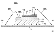
- FIG. 7 is a cross-sectional view showing an example of an LED mounting body by a wire bond method.
- This LED mounting body 100A is obtained by mounting an LED element 110 on a substrate 120.
- the LED element 110 includes, for example, a first conductive clad layer 102 made of, for example, n-GaN, an active layer 103 made of, for example, an InxAlyGa1-xyN layer, and a p- It has a second conductivity type cladding layer 104 made of GaN and has a so-called double heterostructure. As shown in FIG.
- the wire bonding method is such that the electrodes (first conductivity type electrode 104 a and second conductivity type electrode 102 a) of the LED element 110 face upward (face-up), the LED element 110, and the substrate 120.
- the first conductive type circuit pattern 202 and the second conductive type circuit pattern 203 on the base material 201 are electrically bonded by bonding wires 301a and 301b.
- a die bond material is used for bonding the LED element 110 and the substrate 120. 302 is used.
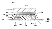
- the electrode (first conductivity type electrode 104a and second conductivity type electrode 102a) surface of the LED element 110 faces the substrate 120 side (face down) as in the LED mounting body 100B shown in FIG.
- conductive pastes 303a and 303b typified by silver paste for electrical connection between the LED element 110 and the substrate 120.
- the electrode surface of the LED element 110 faces the substrate 120 side (face-down, flip chip), and the LED element 110 and the substrate 120 are There is a method of using an anisotropic conductive adhesive 130 in which conductive particles 306 are dispersed in an insulating adhesive binder 305 for electrical connection and adhesion. Since the anisotropic conductive adhesive 130 has a short bonding process, the production efficiency is good.
- the anisotropic conductive adhesive 130 is inexpensive and excellent in transparency, adhesiveness, heat resistance, mechanical strength, electrical insulation, and the like.
- FC mounting LED element can be designed to have a large electrode area by passivation 105 (see FIG. 10), so that bumpless mounting is possible. Further, the light extraction efficiency is improved by providing a reflective film under the light emitting layer.
- gold-tin eutectic bonding is used as in the LED mounting body 100D shown in FIG.
- the electrode connection portion 307 of the LED element 110A is formed of an alloy of gold and tin
- the flux is applied to the substrate 120
- the LED element 110 is mounted, and then the substrate electrode and the substrate electrode are heated.
- This is a crystal bonding method.
- solder connection method has a bad yield because there is an adverse effect on reliability due to chip displacement during heating or flux that could not be cleaned.
- advanced mounting technology is required.
- solder connection construction method that uses a solder paste 303 for electrical connection between the electrode surface of the LED element 110A and the substrate 120 as in the LED mounting body 100E shown in FIG.
- solder connection method since the paste itself has isotropic conductivity, the pn electrodes are short-circuited and the yield is poor.
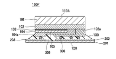
- the electrical connection and adhesion between the LED element 110 and the substrate 120 are performed in an insulating binder 305 as in the example shown in FIG.
- an anisotropic conductive adhesive 130 such as ACF (anisotropic conductive adhesive film) in which conductive particles 306 are dispersed.
- the anisotropic conductive adhesive 130 is filled with an insulating binder 305 between the pn electrodes. Accordingly, the yield is good because short-circuiting hardly occurs. Moreover, since the bonding process is short, the production efficiency is good.
- the active layer 103 is located on the substrate 120 side, so that heat is efficiently transmitted to the substrate 120 side.
- FIGS. 8 and 11 when the electrodes are joined with the conductive pastes 303a and 303b and the solder paste 303, heat can be radiated with high efficiency, but the connection with the conductive pastes 303a and 303b is described above. As shown, connection reliability is poor. Also, as shown in FIG. 10, even when gold-tin eutectic bonding is performed, connection reliability is poor as described above.
- an anisotropic conductive adhesive 130 such as ACF (Anisotropic conduct film) or ACP (Anisotropic conduct paste) without using the conductive pastes 303a and 303b.
- the active layer 103 is disposed near the substrate 120 side, and heat is efficiently transferred to the substrate 120 side. Moreover, since the adhesive strength is high, excellent connection reliability can be obtained.
- JP 2012-19203 A Japanese Patent Laid-Open No. 3-12607 JP 2001-160568 A JP 2012-169263 A
- the thermal conductivity of the cured product of the conventional anisotropic conductive adhesive is about 0.2 W / (m ⁇ K)
- the heat generated from the LED element cannot be sufficiently released to the substrate side.
- the conductive particles in the electrical connection portion serve as a heat dissipation path, so that the heat dissipation is poor.
- the present invention has been proposed in view of such conventional circumstances, and provides an anisotropic conductive adhesive capable of obtaining excellent heat dissipation and connection reliability, and a connection structure using the same. Objective.
- the present inventor can achieve the above-described object by blending conductive particles having a conductive metal layer formed on the surface of resin particles, solder particles, and an inorganic filler. As a result, the present invention has been completed.
- the anisotropic conductive adhesive according to the present invention has a conductive metal layer formed on the surface of resin particles, an average particle diameter of 1 to 10 ⁇ m, and an average particle diameter of the conductive particles.
- Solder particles having an average particle diameter of 25 to 400% and inorganic fillers having an average particle diameter of 100 nm or less are dispersed in an adhesive component.
- connection structure includes a terminal of the first electronic component and a terminal of the second electronic component, conductive particles in which a conductive metal layer is formed on the surface of the resin particles, and solder particles Are electrically connected via an anisotropic conductive adhesive containing an inorganic filler, and the terminal of the first electronic component and the terminal of the second electronic component are the conductive particles. And the solder particles are joined by the solder particles, and the inorganic filler has an average particle size of 100 nm or less.
- the conductive particles are deformed flatly by the pressing force from the opposing terminals during crimping, and the solder particles are crushed and joined by solder, thereby increasing the contact area by metal bonding with each terminal, and excellent Heat dissipation can be obtained. Furthermore, since an inorganic filler having an average particle size of 100 nm or less is blended, the linear expansion coefficient is reduced, and excellent connection reliability can be obtained even for, for example, aluminum-based MCPCB (Metal-Core PCB). it can.
- MCPCB Metal-Core PCB
- the anisotropic conductive adhesive 30 in the present embodiment includes conductive particles 31 having a conductive metal layer formed on the surface of resin particles, solder particles 32, and an inorganic filler (filler). 34) is dispersed in a binder (adhesive component) 33, and the shape thereof is a paste, a film, or the like, and can be appropriately selected according to the purpose.
- FIGS. 2A and 2B are cross-sectional views schematically showing opposing terminals 2 and 3 before and after crimping, respectively.
- pressure bonding refers to pressurization while heating.
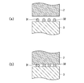
- the conductive particles 31 and the solder particles 32 are included in the binder 33 of the anisotropic conductive adhesive 30 (the detailed configuration will be described later), the conductive particles 31 and Solder particles 32 can be present between the terminals 2 and 3 made of metal. And, at the time of crimping, the conductive particles 31 using resin particles as the core material are deformed flat by the pressing force from the terminals 2 and 3, and elastic repulsion to the deformation occurs, so that the electrical connection state between the terminals 2 and 3 Can be maintained.
- the solder particles 32 are crushed following the flat deformation of the conductive particles 31, and are metal-bonded to the terminals 2 and 3 by soldering by heating, so the area in contact with the terminals 2 and 3 is increased. Heat dissipation and electrical characteristics can be improved.
- the conductive particles 31 having a resin as a core material relieve stress generated due to the difference in thermal expansion coefficient between the substrate and the element, cracks are prevented from occurring in the solder joint portion and connection reliability is improved. be able to.
- the inorganic filler 34 having an average particle size of 100 nm or less is dispersed in the binder 33 of the anisotropic conductive adhesive 30, the linear expansion coefficient of the anisotropic conductive adhesive 30 can be reduced. Excellent connection reliability can be obtained.
- the conductive particles 31 are made of epoxy resin, phenol resin, acrylic resin, acrylonitrile / styrene (AS) resin, benzoguanamine resin, divinylbenzene resin, styrene resin, etc. with a metal such as Au, Ni or Zn. Coated metal-coated resin particles. Since the metal-coated resin particles are easily crushed and easily deformed during compression, the contact area with the wiring pattern can be increased, and variations in the height of the wiring pattern can be absorbed.
- the blending amount of the conductive particles 31 is preferably 1 to 30 vol% with respect to the binder 33 from the viewpoint of connection reliability and insulation reliability.
- the average particle diameter of the conductive particles 31 (D50: the particle diameter when the number or mass larger than a certain particle diameter occupies 50% of the total powder in the particle size distribution of the powder,
- the median diameter is preferably 1 to 10 ⁇ m, more preferably 2 to 6 ⁇ m.
- the solder particles 32 are, for example, Sn—Pb, Pb—Sn—Sb, Sn—Sb, Sn—Pb—Bi, Bi—Sn, Sn—Cu, as defined in JIS Z 3282-1999.
- Sn-Pb-Cu-based, Sn-In-based, Sn-Ag-based, Sn-Pb-Ag-based, Pb-Ag-based, and the like can be appropriately selected according to the electrode material, connection conditions, and the like.
- the shape of the solder particles 32 can be appropriately selected from granular, flake shaped, and the like.
- the solder particles 32 may be covered with an insulating layer in order to improve anisotropy.
- the blending amount of the solder particles 32 is preferably 1 to 30 vol%. If the blending amount of the solder particles 32 is too small, excellent heat dissipation cannot be obtained, and if the blending amount is too large, anisotropy in electrical connection is impaired, and connection reliability cannot be obtained.
- the average particle diameter (D50) of the solder particles 32 is preferably 25 to 400% of the average particle diameter of the conductive particles 31. If the solder particles 32 are too small relative to the conductive particles 31, the solder particles 32 are not captured between the terminals facing each other at the time of pressure bonding, and good solder bonding is not performed, so that excellent heat dissipation cannot be obtained. On the other hand, if the solder particles 32 are too large relative to the conductive particles 31, the anisotropy in electrical connection is impaired, and connection reliability cannot be obtained.
- the inorganic filler 34 for example, silica (SiO 2 ), alumina (Al 2 O 3 ), or the like can be used.
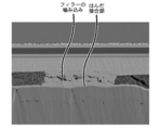
- the average particle diameter (D50: median diameter) of the inorganic filler 34 is 100 nm or less. When the median diameter of the inorganic filler 34 is larger than 100 nm, the inorganic filler 34 enters (bites) around or near the joint between the solder particles 32 and the terminals of the first and second electronic components, and the solder joint Since the contact area becomes smaller, the thermal resistance value increases and the heat dissipation performance deteriorates.
- the blending amount of the inorganic filler 34 is preferably 10 to 40 vol%. If the blending amount of the inorganic filler 34 exceeds 40 vol%, the vf value will increase from the initial stage of pressure bonding, and excellent connection reliability cannot be obtained.
- an adhesive composition used in a conventional anisotropic conductive adhesive or anisotropic conductive film can be used.
- Preferred examples of the adhesive composition include epoxy compounds mainly composed of alicyclic epoxy compounds, heterocyclic epoxy compounds, hydrogenated epoxy compounds, and the like, and curing agents such as acid anhydrides.
- Preferred examples of the alicyclic epoxy compound include those having two or more epoxy groups in the molecule. These may be liquid or solid. Specific examples include glycidyl hexahydrobisphenol A, 3,4-epoxycyclohexenylmethyl-3 ', 4'-epoxycyclohexene carboxylate, and the like. Among them, 3,4-epoxycyclohexenylmethyl-3 ′, 4′-epoxycyclohexenecarboxylate is preferred because it can ensure light transmission suitable for mounting LED elements on the cured product and is excellent in rapid curing. Can be preferably used.
- heterocyclic epoxy compound examples include an epoxy compound having a triazine ring, and particularly preferably 1,3,5-tris (2,3-epoxypropyl) -1,3,5-triazine-2,4, Mention may be made of 6- (1H, 3H, 5H) -trione.
- water-added epoxy compound hydrogenated products of the above-described alicyclic epoxy compounds and heterocyclic epoxy compounds, and other known hydrogenated epoxy resins can be used.
- the alicyclic epoxy compound, heterocyclic epoxy compound and hydrogenated epoxy compound may be used alone, but two or more kinds may be used in combination.
- other epoxy compounds may be used in combination as long as the effects of the present invention are not impaired.
- the curing agent examples include acid anhydrides, imidazole compounds, and dicyan.
- acid anhydrides that are difficult to discolor the cured product particularly alicyclic acid anhydride-based curing agents, can be preferably used.
- methylhexahydrophthalic anhydride etc. can be mentioned preferably.
- the amount of each used is an uncured epoxy compound if there is too little alicyclic acid anhydride curing agent. If the amount is too large, corrosion of the adherend material tends to be accelerated due to the influence of the excess curing agent. Therefore, the alicyclic acid anhydride curing agent is added to 100 parts by mass of the alicyclic epoxy compound.
- the ratio is preferably 80 to 120 parts by mass, more preferably 95 to 105 parts by mass.
- the anisotropic conductive adhesive 30 having such a structure is deformed flat by a pressing force from a terminal to which the conductive particles 31 oppose at the time of pressure bonding, and the solder particles 32 are crushed and soldered by heating to each terminal and the metal Since the contact area is increased by bonding, excellent heat dissipation can be obtained. Moreover, since the inorganic filler 34 whose average particle diameter is 100 nm or less is blended, the linear expansion coefficient of the anisotropic conductive adhesive 30 can be 50 ppm or less. Therefore, even if an aluminum-based MCPCB substrate (Metal-CorePCB) having a high thermal conductivity and a relatively high linear expansion coefficient is used, excellent connection reliability can be obtained.
- Metal-CorePCB Metal-CorePCB
- connection structure and manufacturing method thereof Next, a connection structure using the anisotropic conductive adhesive 30 described above will be described.
- the connection structure in the present embodiment has a first electronic component and a second electronic component, and the terminal of the first electronic component and the terminal of the second electronic component are on the surface of the resin particles.
- the first electronic component is electrically connected through an anisotropic conductive adhesive 30 containing conductive particles 31 on which a conductive metal layer is formed, solder particles 32, and an inorganic filler 34.
- the terminal of the second electronic component and the terminal of the second electronic component are connected by the conductive particles 31 and soldered by the solder particles 32, and the average particle size of the inorganic filler 34 is 100 nm or less.
- a chip such as a driver IC (Integrated Circuit) or LED (Light Emitting Diode) that generates heat is suitable.
- a driver IC Integrated Circuit
- LED Light Emitting Diode
- an aluminum-based MCPCB substrate Metal-Core PCB having a high thermal conductivity but a relatively high linear expansion coefficient is suitable.
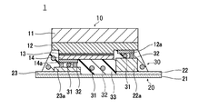
- FIG. 3 is a cross-sectional view showing a configuration example of the LED mounting body 1 which is the connection structure of the present invention.
- the LED element 10 and the substrate 20 the conductive particles 31, the solder particles 32, and the inorganic filler 34 (not shown here) are dispersed in the adhesive component 33.
- the anisotropic conductive adhesive 30 is used for electrical connection and fixing.
- the LED element 10 is formed on an element substrate 11 made of, for example, sapphire, a first conductive clad layer 12 made of, for example, n-GaN, an active layer 13 made of, for example, an InxAlyGa1-xyN layer, and made of, for example, p-GaN. And a second conductivity type cladding layer 14 and has a so-called double heterostructure. Further, a first conductivity type electrode 12 a is provided on a part of the first conductivity type cladding layer 12, and a second conductivity type electrode 14 a is provided on a part of the second conductivity type cladding layer 14. When a voltage is applied between the first conductivity type electrode 12a and the second conductivity type electrode 14a of the LED element 10, carriers are concentrated on the active layer 13 and recombination causes light emission.
- the substrate 20 includes a first conductivity type circuit pattern 22 and a second conductivity type circuit pattern 23 on a base material 21, and the first conductivity type circuit pattern 22 and the second conductivity type circuit pattern 23 are provided on the substrate 21.
- the electrode 22a and the electrode 23a are provided at positions corresponding to the first conductivity type electrode 12a and the second conductivity type electrode 14a of the LED element 10, respectively.
- conductive particles 31 and solder particles 32 having an average particle size smaller than that of the conductive particles 31 are dispersed in the binder 33 as described above.
- the LED mounting body 1 is composed of conductive particles in which the terminals of the LED element 10 (first conductive electrode 12a and second conductive electrode 14a) and the terminals of the substrate 20 (electrodes 22a and 23a) are conductive particles.
- the terminals of the LED elements 10 and the terminals of the substrate 20 are soldered together.
- the linear expansion coefficient of the anisotropic conductive adhesive 30 is 50 ppm or less, and the thermal resistance value of the LED mounting body 1 is 12 K / W or less.
- the heat generated in the active layer 13 of the LED element 10 can be efficiently released to the substrate 20 side, and the LED mounted body 1 can be extended in life while preventing a decrease in light emission efficiency.
- the linear expansion coefficient of the anisotropic conductive adhesive 30 is lower than that of a general anisotropic conductive adhesive, excellent connection reliability can be obtained.
- the solder particles 32 are white or gray achromatic, the light from the active layer 13 is reflected and high brightness can be obtained.
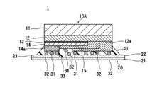
- the LED element 10A for flip-chip mounting has a second conductivity type in which one terminal (first conductivity type electrode 12a) of the LED element 10 is interposed via a passivation 15 made of an insulating material. Since it is provided on the clad layer 14 and is designed to have a larger area than the example shown in FIG. 3, the terminal of the LED element 10 (first conductivity type electrode 12a) and the terminal of the substrate 20 ( More conductive particles 31 and solder particles 32 are captured between the circuit pattern 22) and the circuit pattern 22). As a result, the heat generated in the active layer 13 of the LED element 10 can be released to the substrate 20 side more efficiently.
- the manufacturing method of the LED mounting body in the present embodiment includes the anisotropic conductive adhesive 30 in which the conductive particles 31, the solder particles 32, and the inorganic filler 34 are dispersed in the adhesive component.
- the first electronic component and the second electronic component are thermocompression-bonded between the terminals of the first electronic component and the second electronic component.
- the terminal of the first electronic component and the terminal of the second electronic component are electrically connected via the conductive particles 31, and the terminal of the first electronic component and the terminal of the second electronic component are A connection structure formed by soldering can be obtained.
- the conductive particles 31 are deformed flat by the pressing force from the terminals of the first and second electronic components at the time of pressure bonding, and the solder particles 32 are crushed and soldered by heating. Because of this, the first and second electronic components are metal-bonded to the terminals, so that the contact area between the opposing first and second terminals increases, and excellent heat dissipation and excellent connection reliability can be obtained. .
- the conductive particles 31 having the resin as the core material relieve the stress generated due to the difference in the coefficient of thermal expansion between the substrate 20 and the first and second electronic components, cracks are generated in the solder joints. Can be prevented.
- the average particle diameter of the inorganic filler 34 in the anisotropic conductive adhesive 30 is 100 nm or less, the linear expansion coefficient can be reduced, and excellent connection reliability can be obtained.
- Example> Examples of the present invention will be described in detail below, but the present invention is not limited to these examples.
- an anisotropic conductive adhesive in which solder particles and conductive particles were blended was produced, an LED mounting body was produced, and heat dissipation characteristics, adhesive characteristics, mechanical characteristics, and electrical characteristics were evaluated.
- the production of the anisotropic conductive adhesive the production of the LED mounting body, the evaluation of the heat dissipation characteristics of the LED mounting body, the evaluation of the adhesion characteristics, the evaluation of the mechanical characteristics and the electrical characteristics were performed as follows.
- anisotropic conductive adhesive In an epoxy curing adhesive (epoxy resin (trade name: CEL2021P, manufactured by Daicel Chemical Industries, Ltd.) and acid anhydride (MeHHPA, trade name: MH700, manufactured by Shin Nippon Rika Co., Ltd.)) 10% by volume of conductive particles (product name: AUL705, manufactured by Sekisui Chemical Co., Ltd.) having a mean particle size (D50) of 5 ⁇ m coated with Au on the surface of crosslinked polystyrene resin particles and solder particles having a mean particle size (D50) of 5 ⁇ m (Trade name: M707, manufactured by Senju Metal Industry Co., Ltd.) was mixed with 10 vol% and a filler (inorganic filler) composed of the following particles to prepare an anisotropic conductive adhesive having thermal conductivity.
- epoxy curing adhesive epoxy curing adhesive
- epoxy resin trade name: CEL2021P, manufactured by Daicel Chemical Industries, Ltd.
- acid anhydride MeHHPA,
- anisotropic conductive adhesive to the Au electrode substrate, the LED chip is aligned and mounted, and thermocompression bonding is performed under the conditions of 150 ° C.-10 seconds ⁇ 230 ° C.-30 seconds and a load of 1000 g / chip. It was.
- thermomechanical analyzer TMA / SS7000: manufactured by SII
- the initial evaluation of the high-temperature and high-humidity test is “ ⁇ ” when the variation of the initial Vf from Ref (3.2 V) is less than 2%, and when the initial Vf is 2% or more higher than Ref (3.2 V).
- “Vf high” and rupture of conduction were confirmed OPEN
- “X” was evaluated.
- the evaluation after the high-temperature and high-humidity test was confirmed as “ ⁇ ” when the variation from the initial Vf value was less than 5%, “Vf high” when the variation was 5% or more than the initial Vf, and continuity breaking Case (OPEN) was evaluated as “ ⁇ ”.
- Example 1 As a filler, 10 vol% of silica particles (YA050C, manufactured by Admatechs Co., Ltd.) having an average particle diameter (D50) of 50 nm were blended to prepare an anisotropic conductive adhesive having thermal conductivity.
- silica particles YA050C, manufactured by Admatechs Co., Ltd.
- D50 average particle diameter
- the measurement result of the thermal resistance of the LED mounting body manufactured using the anisotropic conductive adhesive of Example 1 is 11.0 K / W, the die shear strength is 33 N / chip, and the linear expansion coefficient ( ⁇ 1 : Linear expansion coefficient below the glass transition temperature (Tg) was 49 ppm.
- the evaluation result of the high-temperature, high-humidity test of electrical characteristics was “good” at the initial stage, and “good” after the 1000 h test.
- the evaluation result of the thermal shock test of electrical characteristics was “good” in the initial stage, “good” after the 500 cycle test, and “good” after the 1000 cycle test.
- Example 2 As a filler, 20 vol% of silica particles (R812, manufactured by Nippon Aerosil Co., Ltd.) having an average particle diameter (D50) of 7 nm were blended to prepare an anisotropic conductive adhesive having thermal conductivity.
- silica particles R812, manufactured by Nippon Aerosil Co., Ltd.
- D50 average particle diameter
- the measurement results of the thermal resistance of the LED package manufactured using the anisotropic conductive adhesive of Example 2 are 11.0 K / W, the die shear strength is 35 N / chip, and the linear expansion coefficient ( ⁇ 1 ) was 43 ppm.
- the evaluation result of the high-temperature, high-humidity test of electrical characteristics was “good” at the initial stage, and “good” after the 1000 h test.
- the evaluation result of the thermal shock test of electrical characteristics was “good” in the initial stage, “good” after the 500 cycle test, and “good” after the 1000 cycle test.
- Example 3 As a filler, 20 vol% of silica particles (R202, manufactured by Nippon Aerosil Co., Ltd.) having an average particle diameter (D50) of 14 nm were blended to prepare an anisotropic conductive adhesive having thermal conductivity.
- the measurement result of the thermal resistance of the LED mounting body manufactured using the anisotropic conductive adhesive of Example 3 is 11.0 K / W, the die shear strength is 36 N / chip, and the linear expansion coefficient ( ⁇ 1 ) was 44 ppm.
- the evaluation result of the high-temperature, high-humidity test of electrical characteristics was “good” at the initial stage, and “good” after the 1000 h test.
- the evaluation result of the thermal shock test of electrical characteristics was “good” in the initial stage, “good” after the 500 cycle test, and “good” after the 1000 cycle test.
- Example 4 As a filler, 20 vol% of silica particles (YA050C, manufactured by Admatechs) having an average particle diameter (D50) of 50 nm were blended to prepare an anisotropic conductive adhesive having thermal conductivity.
- the measurement results of the thermal resistance of the LED package manufactured using the anisotropic conductive adhesive of Example 4 are 11.0 K / W, the die shear strength is 35 N / chip, and the linear expansion coefficient ( ⁇ 1 ) was 45 ppm.
- the evaluation result of the high-temperature, high-humidity test of electrical characteristics was “good” at the initial stage, and “good” after the 1000 h test.
- the evaluation result of the thermal shock test of electrical characteristics was “good” in the initial stage, “good” after the 500 cycle test, and “good” after the 1000 cycle test.
- Example 5 As a filler, 20 vol% of silica particles (YA100C, manufactured by Admatechs) having an average particle diameter (D50) of 100 nm were blended to prepare an anisotropic conductive adhesive having thermal conductivity.
- YA100C manufactured by Admatechs
- the measurement results of the thermal resistance of the LED package manufactured using the anisotropic conductive adhesive of Example 5 were 11.4 K / W, the die shear strength was 34 N / chip, and the linear expansion coefficient ( ⁇ 1 ) was 46 ppm.
- the evaluation result of the high-temperature, high-humidity test of electrical characteristics was “good” at the initial stage, and “good” after the 1000 h test.
- the evaluation result of the thermal shock test of electrical characteristics was “good” in the initial stage, “good” after the 500 cycle test, and “good” after the 1000 cycle test.
- Example 6 As a filler, 30 vol% of silica particles (YA100C, manufactured by Admatechs Co., Ltd.) having an average particle diameter (D50) of 100 nm were blended to prepare an anisotropic conductive adhesive having thermal conductivity.
- silica particles YA100C, manufactured by Admatechs Co., Ltd.
- D50 average particle diameter
- the measurement results of the thermal resistance of the LED package manufactured using the anisotropic conductive adhesive of Example 6 were 11.6 K / W, the die shear strength was 31 N / chip, and the linear expansion coefficient ( ⁇ 1 ) was 39 ppm.
- the evaluation result of the high-temperature, high-humidity test of electrical characteristics was “good” at the initial stage, and “good” after the 1000 h test.
- the evaluation result of the thermal shock test of electrical characteristics was “good” in the initial stage, “good” after the 500 cycle test, and “good” after the 1000 cycle test.
- Example 7 As a filler, 40 vol% of silica particles (YA100C, manufactured by Admatechs) with an average particle diameter (D50) of 100 nm were blended to prepare an anisotropic conductive adhesive having thermal conductivity.
- silica particles YA100C, manufactured by Admatechs
- D50 average particle diameter
- the measurement results of the thermal resistance of the LED package manufactured using the anisotropic conductive adhesive of Example 7 were 11.9 K / W, the die shear strength was 30 N / chip, and the linear expansion coefficient ( ⁇ 1 ) was 35 ppm.
- the evaluation result of the high-temperature, high-humidity test of electrical characteristics was “good” at the initial stage, and “good” after the 1000 h test.
- the evaluation result of the thermal shock test of electrical characteristics was “good” in the initial stage, “good” after the 500 cycle test, and “good” after the 1000 cycle test.
- the measurement result of the thermal resistance of the LED mounting body manufactured using the anisotropic conductive adhesive of Comparative Example 1 is 11.0 K / W
- the die shear strength is 32 N / chip
- the linear expansion coefficient ( ⁇ 1 ) was 62 ppm.
- the evaluation result of the high-temperature, high-humidity test of electrical characteristics was “good” at the initial stage, and “good” after the 1000 h test.
- the evaluation result of the thermal shock test of electrical characteristics was “good” in the initial stage, “good” after the 500 cycle test, and “poor” after the 1000 cycle test.
- ⁇ Comparative example 2> As a filler, 20 vol% of silica particles having an average particle diameter (D50) of 200 nm (Hi-Plessa 0.2, manufactured by Ube Nitto Kasei Co., Ltd.) were blended to prepare an anisotropic conductive adhesive having thermal conductivity.
- D50 average particle diameter
- Hi-Plessa 0.2 manufactured by Ube Nitto Kasei Co., Ltd.
- the measurement results of the thermal resistance of the LED package manufactured using the anisotropic conductive adhesive of Comparative Example 2 are 13.2 K / W, the die shear strength is 26 N / chip, and the linear expansion coefficient ( ⁇ 1 ) was 47 ppm.
- the evaluation result of the high-temperature, high-humidity test of electrical characteristics was “good” at the initial stage, and “good” after the 1000 h test.
- the evaluation result of the thermal shock test of electrical characteristics was “good” in the initial stage, “good” after the 500 cycle test, and “poor” after the 1000 cycle test.
- 20 vol% of alumina particles (Sumicorundum, manufactured by Sumitomo Chemical Co., Ltd.) having an average particle diameter (D50) of 400 nm were blended to prepare an anisotropic conductive adhesive having thermal conductivity.
- the measurement result of the thermal resistance of the LED mounting body manufactured using the anisotropic conductive adhesive of Comparative Example 3 is 14.1 K / W
- the die shear strength is 24 N / chip
- the linear expansion coefficient ( ⁇ 1 ) was 49 ppm.
- the evaluation result of the high-temperature and high-humidity test of the electrical characteristics was ⁇ at the initial stage, and Vf was high after the 1000 h test.
- the evaluation result of the thermal shock test of electrical characteristics was “good” in the initial stage, “good” after the 500 cycle test, and “poor” after the 1000 cycle test.
- ⁇ Comparative example 4> As a filler, 20 vol% of silica particles having an average particle diameter (D50) of 1.0 ⁇ m (High Plessa 1.0, manufactured by Ube Nitto Kasei Co., Ltd.) were blended to prepare an anisotropic conductive adhesive having thermal conductivity.
- D50 average particle diameter
- High Plessa 1.0 manufactured by Ube Nitto Kasei Co., Ltd.
- the measurement result of the thermal resistance of the LED mounting body manufactured using the anisotropic conductive adhesive of Comparative Example 4 is 12.8 K / W
- the die shear strength is 27 N / chip
- the linear expansion coefficient ( ⁇ 1 ) was 48 ppm.
- the evaluation result of the high-temperature and high-humidity test of the electrical characteristics was ⁇ at the initial stage, and Vf was high after the 1000 h test.
- the evaluation result of the thermal shock test of the electrical characteristics was “ ⁇ ” in the initial stage, “Vf” after the 500 cycle test, and “x” after the 1000 cycle test.
- silica particles (YA100C, manufactured by Admatechs Co., Ltd.) having an average particle diameter (D50) of 100 nm were blended in an amount of 50 vol% to prepare an anisotropic conductive adhesive having thermal conductivity.
- the measurement result of the thermal resistance of the LED mounting body manufactured using the anisotropic conductive adhesive of Comparative Example 5 is 12.7 K / W, the die shear strength is 25 N / chip, and the linear expansion coefficient ( ⁇ 1 ) was 31 ppm.
- the evaluation result of the high-temperature and high-humidity test of the electrical characteristics was Vf high in the initial stage, and x after the 1000 h test.
- the evaluation result of the thermal shock test of the electrical characteristics was Vf high in the initial stage, and x after the 500 cycle test.
- FIG. 5 is a graph showing the thermal resistance value with respect to the filler particle size. From this graph, it is understood that the thermal resistance value can be lowered by setting the filler particle size to 100 nm or less.
- Example 1 the thermal resistance value of the LED mounting sample using ACP in which 10 vol% of 50 nm filler was added to the binder resin was 11.0 (K / W), and no comparison was made. The heat dissipation equivalent to Example 1 was maintained. In addition, the die shear strength was 33 N / chip, which was higher than that of Comparative Example 1. The linear expansion coefficient was 49 ppm, which was lower than that of Comparative Example 1. Further, in the lighting test under the environment of 85 ° C. and 85% RH, the electrical connection reliability was good in the test 1000 h. Also, good electrical connection reliability was obtained even after 500 cycles and 1000 cycles of the thermal shock test.
- the thermal resistance value of the LED mounting sample using ACP in which 20 vol% of 7 nm filler is added to the binder resin is 11.0 (K / W), which is equal to that of Comparative Example 1.
- the die shear strength was 35 N / chip, which was higher than that of Comparative Example 1.
- the linear expansion coefficient was 43 ppm, which was lower than that of Comparative Example 1.
- the electrical connection reliability was good in the test 1000 h. Also, good electrical connection reliability was obtained even after 500 cycles and 1000 cycles of the thermal shock test.
- the thermal resistance value of the LED mounting sample using ACP in which 20 vol% of 14 nm filler is added to the binder resin is 11.0 (K / W), which is equal to that of Comparative Example 1.
- the die shear strength was 36 N / chip, which was higher than that of Comparative Example 1.
- the linear expansion coefficient was 44 ppm, which was lower than that of Comparative Example 1.
- the electrical connection reliability was good in the test 1000 h. Also, good electrical connection reliability was obtained even after 500 cycles and 1000 cycles of the thermal shock test.
- the heat resistance value of the LED mounting sample using ACP in which 20 vol% of 50 nm filler is added to the binder resin is 11.0 (K / W), which is equal to that of Comparative Example 1.
- the die shear strength was 35 N / chip, which was higher than that of Comparative Example 1.
- the linear expansion coefficient was 45 ppm, which was lower than that of Comparative Example 1.
- the electrical connection reliability was good in the test 1000 h. Also, good electrical connection reliability was obtained even after 500 cycles and 1000 cycles of the thermal shock test.
- the thermal resistance value of the LED mounting sample using ACP in which 20 vol% of 100 nm filler is added to the binder resin is 11.4 (K / W), which is equal to that of Comparative Example 1.
- the die shear strength was 34 N / chip, which was higher than that of Comparative Example 1.
- the linear expansion coefficient was 46 ppm, which was lower than that of Comparative Example 1.
- the electrical connection reliability was good in the test 1000 h. Also, good electrical connection reliability was obtained even after 500 cycles and 1000 cycles of the thermal shock test.
- Example 6 the heat resistance value of the LED mounting sample using ACP in which 30 vol% of 100 nm filler is added to the binder resin is 11.6 (K / W), which is the same heat dissipation as Comparative Example 1.
- the die shear strength was 31 N / chip, and the adhesive strength equivalent to that of Comparative Example 1 was maintained.
- the linear expansion coefficient was 39 ppm, which was lower than that of Comparative Example 1.
- the electrical connection reliability was good in the test 1000 h. Also, good electrical connection reliability was obtained even after 500 cycles and 1000 cycles of the thermal shock test.
- the heat resistance value of the LED mounting sample using ACP in which 40 vol% of 100 nm filler is added to the binder resin is 11.9 (K / W), which is equal to that of Comparative Example 1.
- the die shear strength was 30 N / chip, and the adhesive strength equivalent to that of Comparative Example 1 was maintained.
- the linear expansion coefficient was 35 ppm, which was lower than that of Comparative Example 1.
- the electrical connection reliability was good in the test 1000 h. Also, good electrical connection reliability was obtained even after 500 cycles and 1000 cycles of the thermal shock test.
- the thermal resistance value of the LED mounting sample using ACP in which no filler was blended with the binder resin was 11.0 (K / W).
- the die shear strength was 32 N / chip.
- the linear expansion coefficient was 62 ppm.
- the electrical connection reliability was good in the test 1000 h. Also, good electrical connection reliability was obtained after 500 cycles of the thermal shock test, but good electrical connection reliability could not be obtained because OPEN occurred after 1000 cycles.
- Comparative Example 3 in the LED mounting sample using ACP in which 20% by volume of a filler of 400 nm is added to the binder resin, biting of the filler occurs and the thermal resistance value is 14.1 (K / W). Thus, the heat dissipation was worse than that of Comparative Example 1.
- the die shear strength was 24 N / chip, which was worse than that of Comparative Example 1.
- the linear expansion coefficient was 49 ppm, which was lower than that of Comparative Example 1.
- the initial electrical characteristics were good, but an increase in the Vf value was confirmed in the test 1000 h. Also, good electrical connection reliability was obtained after 500 cycles of the thermal shock test, but good electrical connection reliability could not be obtained because OPEN occurred after 1000 cycles.
- Comparative Example 5 in the LED mounting sample using ACP in which 50 vol% of 100 nm filler was added to the binder resin, filler biting occurred and the thermal resistance value was 12.7 (K / W). Thus, the heat dissipation was worse than that of Comparative Example 1.
- the die shear strength was 25 N / chip, which was worse than that of Comparative Example 1.
- the linear expansion coefficient was 31 ppm, which was lower than that of Comparative Example 1.
- the Vf value was high from the beginning, and OPEN was generated after the lighting test 1000h and the thermal shock test 500 cycles in an environment of 85 ° C. and 85% RH, so that good electrical connection reliability could not be obtained.
- SYMBOLS 1 LED mounting body (connection structure) 2, 3 ... Terminal 10 ... LED element (1st electronic component) 11 ... Element board
Landscapes
- Chemical & Material Sciences (AREA)
- Organic Chemistry (AREA)
- Chemical Kinetics & Catalysis (AREA)
- Spectroscopy & Molecular Physics (AREA)
- Dispersion Chemistry (AREA)
- Health & Medical Sciences (AREA)
- Physics & Mathematics (AREA)
- Medicinal Chemistry (AREA)
- Polymers & Plastics (AREA)
- Adhesives Or Adhesive Processes (AREA)
- Wire Bonding (AREA)
- Led Device Packages (AREA)
- Conductive Materials (AREA)
- Non-Insulated Conductors (AREA)
Abstract
本発明は、優れた放熱性及び接続信頼性が得られる異方性導電接着剤を提供することを目的とする。本発明の異方性導電接着剤30は、樹脂粒子の表面に導電性金属層が形成され、平均粒径が1~10μmである導電性粒子31と、平均粒径が導電性粒子31の平均粒径の25~400%であるはんだ粒子32と、平均粒径が100nm以下である無機充填材34とが接着剤成分33に分散されている。圧着時に導電性粒子31が押圧により扁平変形するとともに、はんだ粒子32が潰れてはんだ接合されるため、対向する端子間のとの接触面積が増加し、優れた放熱性を得ることができる。さらに、平均粒径が100nm以下である無機充填材34が配合されているため、線膨張率を低下させ、例えばアルミベースのMCPCB(Metal Core PCB)に対しても、優れた接続信頼性を得ることができる。
Description
本発明は、接着剤成分中に導電性粒子が分散された異方性導電接着剤に関し、特に、ドライバーIC(Integrated Circuit)、LED(Light Emitting Diode)等のチップ(素子)が発する熱を放熱することが可能な異方性導電接着剤及びこれを用いた接続構造体に関する。
従来、LED素子を基板に実装する工法として、ワイヤーボンド(WB)工法が用いられている。
図7は、ワイヤーボンド工法によるLED実装体の一例を示す断面図である。
このLED実装体100Aは、基板120上にLED素子110を実装したものである。
ここで、LED素子110は、例えばサファイヤからなる素子基板101上に、例えばn-GaNからなる第1導電型クラッド層102と、例えばInxAlyGa1-x-yN層からなる活性層103と、例えばp-GaNからなる第2導電型クラッド層104とを備え、いわゆるダブルヘテロ構造を有している。
ワイヤーボンド工法は、図7に示すように、LED素子110の電極(第1導電型電極104a及び第2導電型電極102a)面を上に向け(フェイスアップ)、そのLED素子110と、基板120の基材201上の第1導電型用回路パターン202と第2導電型用回路パターン203の電気的接合をボンディングワイヤ301a、301bで行い、LED素子110と基板120との接着には、ダイボンド材302を用いる。
図7は、ワイヤーボンド工法によるLED実装体の一例を示す断面図である。
このLED実装体100Aは、基板120上にLED素子110を実装したものである。
ここで、LED素子110は、例えばサファイヤからなる素子基板101上に、例えばn-GaNからなる第1導電型クラッド層102と、例えばInxAlyGa1-x-yN層からなる活性層103と、例えばp-GaNからなる第2導電型クラッド層104とを備え、いわゆるダブルヘテロ構造を有している。
ワイヤーボンド工法は、図7に示すように、LED素子110の電極(第1導電型電極104a及び第2導電型電極102a)面を上に向け(フェイスアップ)、そのLED素子110と、基板120の基材201上の第1導電型用回路パターン202と第2導電型用回路パターン203の電気的接合をボンディングワイヤ301a、301bで行い、LED素子110と基板120との接着には、ダイボンド材302を用いる。
しかし、このようなワイヤーボンド工法で電気的接続を得る方法では、電極(第1導電型電極104a及び第2導電型電極102a)からのボンディングワイヤ301a、301bの物理的破断・剥離のリスクがあるため、より信頼性の高い技術が求められている。さらに、ダイボンド材302の硬化プロセスは、オーブン硬化で行われるため、生産に時間が掛かる。
ワイヤーボンドを用いない工法として、図8に示すLED実装体100Bのように、LED素子110の電極(第1導電型電極104a及び第2導電型電極102a)面を基板120側に向け(フェイスダウン、フリップチップ)、そのLED素子110と基板120との電気的接続に、銀ペーストに代表される導電性ペースト303a、303bを用いる方法がある。
しかし、導電性ペースト303a、303bは、接着力が弱いため、封止樹脂304による補強が必要である。さらに、封止樹脂304の硬化プロセスは、オーブン硬化で行われるため、生産に時間が掛かる。
導電性ペーストを用いない工法として、図9に示すLED実装体100Cのように、LED素子110の電極面を基板120側に向け(フェイスダウン、フリップチップ)、そのLED素子110と基板120との電気的接続及び接着に、絶縁性の接着剤バインダー305中に導電性粒子306を分散させた異方性導電接着剤130を用いる方法がある。異方性導電接着剤130は、接着プロセスが短いため、生産効率が良い。また、異方性導電接着剤130は、安価であり、透明性、接着性、耐熱性、機械的強度、電気絶縁性等に優れている。
また、近年、フリップチップ(FC)実装をするためのLED素子が開発されている。このFC実装用LED素子は、パッシベーション105により(図10参照)、電極面積を大きく取る設計が可能であるため、バンプレス実装が可能となる。また、発光層の下に反射膜を設けることによって光取り出し効率が良くなる。
FC実装用LED素子を基板に実装する工法としては、図10に示すLED実装体100Dのように、金スズ共晶接合が用いられている。金スズ共晶接合は、LED素子110Aの電極接続部307を金とスズの合金で形成し、フラックスを基板120に塗布し、LED素子110を搭載した後、加熱することで基板電極と、共晶接合させる工法である。しかし、このようなはんだ接続工法は、加熱中のチップズレや洗浄しきれなかったフラックスによる信頼性への悪影響があるため歩留まりが悪い。また、高度な実装技術が必要である。
金スズ共晶を用いない工法として、図11に示すLED実装体100Eのように、LED素子110Aの電極面と基板120との電気的接続に、はんだペースト303を用いるはんだ接続工法がある。しかし、このようなはんだ接続工法は、ペースト自体が等方性の導電性を有するため、pn電極間がショートしてしまい歩留まりが悪い。
はんだペーストを用いない工法として、図12に示すLED実装体100Fのように、LED素子110と基板120との電気的接続及び接着に、図9に示す例と同様、絶縁性のバインダー305中に導電性粒子306を分散させたACF(異方性導電接着フィルム)などの異方性導電接着剤130を用いる方法がある。異方性導電接着剤130は、pn電極間に絶縁性のバインダー305が充填される。よって、ショートが発生しにくいため歩留まりが良い。また、接着プロセスが短いため、生産効率が良い。
ところで、上述したLED素子110、110Aの活性層(ジャンクション)103は、光の他に多くの熱を発生し、発光層温度(Tj=ジャンクション温度)が100℃以上になると、LEDの発光効率が低下し、LEDの寿命が短くなる。このため、活性層103の熱を効率良く逃がすための構造が必要である。
図7に示すようなWB実装では、活性層103がLED素子110の上部の基板120から離れた場所に位置するため、活性層103から発生した熱が基板120側に効率良く伝わらないため放熱性が悪い。
また、図8、10、11に示すようなフリップチップ実装を行うと、活性層103が基板120側に位置するため、熱が基板120側に効率良く伝わる。図8、11に示すように、電極同士を導電性ペースト303a、303bやはんだペースト303で接合した場合、高効率で放熱することができるが、導電性ペースト303a、303bによる接続は、上記で述べたように接続信頼性が悪い。また、図10に示すように、金スズ共晶接合を行った場合も、上記で述べたのと同様に接続信頼性が悪い。
また、図9、12に示すように、導電性ペースト303a、303bを用いずにACF(Anisotropic conduct film)やACP(Anisotropic conduct paste)等の異方性導電接着剤130でフリップチップ実装することで、活性層103が基板120側近くに配置され、熱が基板120側に効率良く伝わる。また、接着力が高いため、優れた接続信頼性が得られる。
しかしながら、従来の異方性導電接着剤の硬化物の熱伝導率は、0.2W/(m・K)程度であるため、LED素子から発生する熱を基板側に十分に逃がすことができない。また、異方性導電接着剤を用いたフリップチップ実装では、電気接続部分の導電性粒子のみが放熱路となるため、放熱性が悪い。
また、従来の異方性導電接着剤では、線膨張率が比較的高い基板、例えば、アルミベースのMCPCB(Metal Core PCB)に対して、優れた接続信頼性を得ることが困難であった。
本発明は、このような従来の実情に鑑みて提案されたものであり、優れた放熱性及び接続信頼性が得られる異方性導電接着剤及びこれを用いた接続構造体を提供することを目的とする。
本件発明者は、鋭意検討を行った結果、樹脂粒子の表面に導電性金属層が形成された導電性粒子と、はんだ粒子と、無機充填材とを配合することにより、上述の目的を達成できることを見出し、本発明を完成させるに至った。
すなわち、本発明に係る異方性導電接着剤は、樹脂粒子の表面に導電性金属層が形成され、平均粒径が1~10μmである導電性粒子と、平均粒径が前記導電性粒子の平均粒径の25~400%であるはんだ粒子と、平均粒径が100nm以下である無機充填材とが接着剤成分に分散されてなることを特徴としている。
また、本発明に係る接続構造体は、第1の電子部品の端子と、第2の電子部品の端子とが、樹脂粒子の表面に導電性金属層が形成された導電性粒子と、はんだ粒子と、無機充填材とを含有する異方性導電接着剤を介して電気的に接続されてなり、前記第1の電子部品の端子と前記第2の電子部品の端子とが、前記導電性粒子により接続されるともに、前記はんだ粒子によりはんだ接合されてなり、前記無機充填材の平均粒径が、100nm以下であることを特徴としている。
本発明によれば、圧着時に導電性粒子が対向する端子からの押圧力により扁平変形するとともに、はんだ粒子が潰れてはんだ接合され、これにより各端子と金属結合して接触面積が増加し、優れた放熱性を得ることができる。さらに、平均粒径が100nm以下である無機充填材が配合されているため、線膨張率を低下させ、例えばアルミベースのMCPCB(Metal CorePCB)に対しても、優れた接続信頼性を得ることができる。
以下、本発明の実施の形態について、図面を参照しながら下記順序にて詳細に説明する。
1.異方性導電接着剤及びその製造方法
2.接続構造体及びその製造方法
3.実施例
1.異方性導電接着剤及びその製造方法
2.接続構造体及びその製造方法
3.実施例
<1.異方性導電接着剤及びその製造方法>
図1に示すように、本実施の形態における異方性導電接着剤30は、樹脂粒子の表面に導電性金属層が形成された導電性粒子31と、はんだ粒子32と、無機充填材(フィラー)34とがバインダー(接着剤成分)33中に分散されたものであり、その形状は、ペースト、フィルムなどであり、目的に応じて適宜選択することができる。
図1に示すように、本実施の形態における異方性導電接着剤30は、樹脂粒子の表面に導電性金属層が形成された導電性粒子31と、はんだ粒子32と、無機充填材(フィラー)34とがバインダー(接着剤成分)33中に分散されたものであり、その形状は、ペースト、フィルムなどであり、目的に応じて適宜選択することができる。
図2(a)(b)は、それぞれ圧着前及び圧着後における対向する端子2、3を模式的に示す断面図である。なお、本明細書における「圧着」とは、加熱しながら加圧することをいうものとする。
本実施の形態では、異方性導電接着剤30のバインダー33中に導電性粒子31とはんだ粒子32が含まれていることから(詳細な構成は後述する)、圧着前において導電性粒子31とはんだ粒子32とを金属からなる端子2、3間に存在させることができる。そして、圧着時、芯材に樹脂粒子を使用した導電性粒子31が端子2、3からの押圧力により扁平変形し、変形に対する弾性反発が生じるため、端子2、3間における電気的な接続状態を維持することができる。また、圧着時、はんだ粒子32が導電性粒子31の扁平変形に追従して潰れ、加熱によるはんだ接合により各端子2、3と金属結合するため、端子2、3と接触する面積が増大し、放熱性及び電気特性を向上させることができる。また、樹脂を芯材とする導電性粒子31が、基板と素子の熱膨張率の違いにより発生する応力を緩和するため、はんだ接合部にクラックが発生するのを防ぎ、接続信頼性を向上させることができる。さらに、異方性導電接着剤30のバインダー33中に平均粒径が100nm以下の無機充填材34が分散されているため、異方性導電接着剤30の線膨張係数を低下させることができ、優れた接続信頼性を得ることができる。
本実施の形態では、異方性導電接着剤30のバインダー33中に導電性粒子31とはんだ粒子32が含まれていることから(詳細な構成は後述する)、圧着前において導電性粒子31とはんだ粒子32とを金属からなる端子2、3間に存在させることができる。そして、圧着時、芯材に樹脂粒子を使用した導電性粒子31が端子2、3からの押圧力により扁平変形し、変形に対する弾性反発が生じるため、端子2、3間における電気的な接続状態を維持することができる。また、圧着時、はんだ粒子32が導電性粒子31の扁平変形に追従して潰れ、加熱によるはんだ接合により各端子2、3と金属結合するため、端子2、3と接触する面積が増大し、放熱性及び電気特性を向上させることができる。また、樹脂を芯材とする導電性粒子31が、基板と素子の熱膨張率の違いにより発生する応力を緩和するため、はんだ接合部にクラックが発生するのを防ぎ、接続信頼性を向上させることができる。さらに、異方性導電接着剤30のバインダー33中に平均粒径が100nm以下の無機充填材34が分散されているため、異方性導電接着剤30の線膨張係数を低下させることができ、優れた接続信頼性を得ることができる。
導電性粒子31は、エポキシ樹脂、フェノール樹脂、アクリル樹脂、アクリロニトリル・スチレン(AS)樹脂、ベンゾグアナミン樹脂、ジビニルベンゼン系樹脂、スチレン系樹脂等の樹脂粒子の表面をAu、Ni、Zn等の金属で被覆した金属被覆樹脂粒子である。金属被覆樹脂粒子は、圧縮時に潰れやすく、変形し易いため、配線パターンとの接触面積を大きくでき、また、配線パターンの高さのバラツキを吸収することができる。
また、導電性粒子31の配合量は、接続信頼性及び絶縁信頼性の観点から、バインダー33に対して1~30vol%であることが好ましい。また、導電性粒子31の平均粒径(D50:粉体の粒径分布において,ある粒子径より大きい個数又は質量が,全粉体のそれの50%を占めるときの粒子径で、本明細書ではメジアン径をいう)は、1~10μmであることが好ましく、より好ましくは2~6μmである。
はんだ粒子32は、例えばJIS Z 3282-1999に規定されている、Sn-Pb系、Pb-Sn-Sb系、Sn-Sb系、Sn-Pb-Bi系、Bi-Sn系、Sn-Cu系、Sn-Pb-Cu系、Sn-In系、Sn-Ag系、Sn-Pb-Ag系、Pb-Ag系などから、電極材料や接続条件などに応じて適宜選択することができる。また、はんだ粒子32の形状は、粒状、燐片状などから適宜選択することができる。なお、はんだ粒子32は、異方性を向上させるために絶縁層で被覆されていても構わない。
はんだ粒子32の配合量は、1~30vol%であることが好ましい。はんだ粒子32の配合量が少なすぎると優れた放熱性が得られなくなり、配合量が多すぎると電気的接続における異方性が損なわれ、接続信頼性を得ることができない。
また、はんだ粒子32の平均粒径(D50)は、導電性粒子31の平均粒径の25~400%であることが好ましい。はんだ粒子32が導電性粒子31に対して小さすぎると、圧着時にはんだ粒子32が対向する端子間に捕捉されず、良好なはんだ接合が行われず、優れた放熱性を得ることができない。一方、はんだ粒子32が導電性粒子31に対して大きすぎると、電気的接続における異方性が損なわれ、接続信頼性を得ることができない。
無機充填材34は、例えば、シリカ(SiO2)、アルミナ(Al2O3)などを用いることができる。無機充填材34の平均粒径(D50:メジアン径)は、100nm以下である。無機充填材34のメジアン径が100nmより大きいと、はんだ粒子32と第1、第2の電子部品の端子の接合部の周辺や近傍に無機充填材34が入り込み(噛み込み)、当該はんだ接合部の接触面積が小さくなるため、熱抵抗値が上昇し、放熱性が悪化してしまう。
また、無機充填材34の配合量は、10~40vol%であることが好ましい。無機充填材34の配合量が40vol%を超えると、圧着初期の段階からvf値が上昇し、優れた接続信頼性を得ることができない。
バインダー33としては、従来の異方性導電接着剤や異方性導電フィルムにおいて使用されている接着剤組成物を利用することができる。接着剤組成物としては、脂環式エポキシ化合物や複素環系エポキシ化合物や水素添加エポキシ化合物等を主成分としたエポキシ化合物、及び酸無水物等の硬化剤が好ましく挙げられる。
脂環式エポキシ化合物としては、分子内に2つ以上のエポキシ基を有するものが好ましく挙げられる。これらは、液状であっても固体状であってもよい。具体的には、グリシジルヘキサヒドロビスフェノールA、3,4-エポキシシクロヘキセニルメチル-3’,4’-エポキシシクロヘキセンカルボキシレート等を挙げることができる。中でも、硬化物にLED素子の実装等に適した光透過性を確保でき、速硬化性にも優れている点から、3,4-エポキシシクロヘキセニルメチル-3’,4’-エポキシシクロヘキセンカルボキシレートを好ましく使用することができる。
複素環状エポキシ化合物としては、トリアジン環を有するエポキシ化合物を挙げることができ、特に好ましくは1,3,5-トリス(2,3-エポキシプロピル)-1,3,5-トリアジン-2,4,6-(1H,3H,5H)-トリオンを挙げることができる。
水添加エポキシ化合物としては、先述の脂環式エポキシ化合物や複素環系エポキシ化合物の水素添加物や、その他公知の水素添加エポキシ樹脂を使用することができる。
脂環式エポキシ化合物や複素環系エポキシ化合物や水素添加エポキシ化合物は、単独で使用してもよいが、2種以上を併用することができる。また、これらのエポキシ化合物に加えて本発明の効果を損なわない限り、他のエポキシ化合物を併用してもよい。例えば、ビスフェノールA、ビスフェノールF、ビスフェノールS、テトラメチルビスフェノールA、ジアリールビスフェノールA、ハイドロキノン、カテコール、レゾルシン、クレゾール、テトラブロモビスフェノールA、トリヒドロキシビフェニル、ベンゾフェノン、ビスレゾルシノール、ビスフェノールヘキサフルオロアセトン、テトラメチルビスフェノールA、テトラメチルビスフェノールF、トリス(ヒドロキシフェニル)メタン、ビキシレノール、フェノールノボラック、クレゾールノボラック等の多価フェノールとエピクロルヒドリンとを反応させて得られるグリシジルエーテル;グリセリン、ネオペンチルグリコール、エチレングリコール、プロピレングリコール、ヘキシレングリコール、ポリエチレングリコール、ポリプロピレングリコール等の脂肪族多価アルコールとエピクロルヒドリンとを反応させて得られるポリグリシジルエーテル;p-オキシ安息香酸、β-オキシナフトエ酸のようなヒドロキシカルボン酸とエピクロルヒドリンとを反応させて得られるグリシジルエーテルエステル;フタル酸、メチルフタル酸、イソフタル酸、テレフタル酸、テトラハイドロフタル酸、エンドメチレンテトラハイドロフタル酸、エンドメチレンヘキサハイドロフタル酸、トリメット酸、重合脂肪酸のようなポリカルボン酸から得られるポリグリシジルエステル;アミノフェノール、アミノアルキルフェノールから得られるグリシジルアミノグリシジルエーテル;アミノ安息香酸から得られるグリシジルアミノグリシジルエステル;アニリン、トルイジン、トリブロムアニリン、キシリレンジアミン、ジアミノシクロヘキサン、ビスアミノメチルシクロヘキサン、4,4’-ジアミノジフェニルメタン、4,4’-ジアミノジフェニルスルホン等から得られるグリシジルアミン;エポキシ化ポリオレフィン等の公知のエポキシ樹脂類が挙げられる。
硬化剤としては、酸無水物、イミダゾール化合物、ジシアン等を挙げることができる。中でも、硬化物を変色させ難い酸無水物、特に脂環式酸無水物系硬化剤を好ましく使用できる。具体的には、メチルヘキサヒドロフタル酸無水物等を好ましく挙げることができる。
接着剤組成物において、脂環式エポキシ化合物と脂環式酸無水物系硬化剤とを使用する場合、それぞれの使用量は、脂環式酸無水物系硬化剤が少なすぎると未硬化エポキシ化合物が多くなり、多すぎると余剰の硬化剤の影響で被着体材料の腐食が促進される傾向があるので、脂環式エポキシ化合物100質量部に対し、脂環式酸無水物系硬化剤を、好ましくは80~120質量部、より好ましくは95~105質量部の割合で使用する。
このような構成からなる異方性導電接着剤30は、圧着時に導電性粒子31が対向する端子からの押圧力により扁平変形するとともに、はんだ粒子32が潰れ、加熱によるはんだ接合により各端子と金属結合して接触面積が増加するため、優れた放熱性を得ることができる。また、平均粒径が100nm以下である無機充填材34を配合しているため、異方性導電接着剤30の線膨張係数を50ppm以下とすることができる。よって、熱伝導率は高いが線膨張率が比較的高いアルミベースのMCPCB基板(Metal CorePCB)を使用しても、優れた接続信頼性を得ることができる。
<2.接続構造体及びその製造方法>
次に、前述した異方性導電接着剤30を用いた接続構造体について説明する。本実施の形態における接続構造体は、第1の電子部品と第2の電子部品を有するもので、第1の電子部品の端子と、第2の電子部品の端子とが、樹脂粒子の表面に導電性金属層が形成された導電性粒子31と、はんだ粒子32と、無機充填材34とを含有する異方性導電接着剤30を介して電気的に接続されてなり、第1の電子部品の端子と第2の電子部品の端子とが、導電性粒子31により接続されるともに、はんだ粒子32によりはんだ接合されてなり、無機充填材34の平均粒径が、100nm以下である。
次に、前述した異方性導電接着剤30を用いた接続構造体について説明する。本実施の形態における接続構造体は、第1の電子部品と第2の電子部品を有するもので、第1の電子部品の端子と、第2の電子部品の端子とが、樹脂粒子の表面に導電性金属層が形成された導電性粒子31と、はんだ粒子32と、無機充填材34とを含有する異方性導電接着剤30を介して電気的に接続されてなり、第1の電子部品の端子と第2の電子部品の端子とが、導電性粒子31により接続されるともに、はんだ粒子32によりはんだ接合されてなり、無機充填材34の平均粒径が、100nm以下である。
本実施の形態における第1の電子部品としては、熱を発するドライバーIC(Integrated Circuit)、LED(Light Emitting Diode)等のチップ(素子)が好適である。また第2の部品としては、熱伝導率は高いが線膨張率が比較的高いアルミベースのMCPCB基板(Metal CorePCB)等が好適である。
図3は、本発明の接続構造体であるLED実装体1の構成例を示す断面図である。このLED実装体1は、LED素子10と基板20とを、前述した導電性粒子31と、はんだ粒子32と、無機充填材34(ここでは図示せず)とが接着剤成分33中に分散された異方性導電接着剤30を用いて電気的に接続するとともに固着したものである。
LED素子10は、例えばサファイヤからなる素子基板11上に、例えばn-GaNからなる第1導電型クラッド層12と、例えばInxAlyGa1-x-yN層からなる活性層13と、例えばp-GaNからなる第2導電型クラッド層14とを備え、いわゆるダブルヘテロ構造を有する。また、第1導電型クラッド層12上の一部に第1導電型電極12aを備え、第2導電型クラッド層14上の一部に第2導電型電極14aを備える。LED素子10の第1導電型電極12aと第2導電型電極14aとの間に電圧を印加すると、活性層13にキャリアが集中し、再結合することにより発光が生じる。
基板20は、基材21上に第1導電型用回路パターン22と、第2導電型用回路パターン23とを備え、これら第1導電型用回路パターン22及び第2導電型用回路パターン23上には、LED素子10の第1導電型電極12a及び第2導電型電極14aに対応する位置にそれぞれ電極22a及び電極23aが設けられている。
異方性導電接着剤30は、前述と同様、導電性粒子31と、導電性粒子31よりも平均粒径が小さいはんだ粒子32とがバインダー33中に分散されている。
図3に示すように、LED実装体1は、LED素子10の端子(第1導電型電極12a、第2導電型電極14a)と、基板20の端子(電極22a、23a)とが導電性粒子31を介して電気的に接続され、これらLED素子10の端子と基板20の端子とがはんだ接合されている。
また、異方性導電接着剤30の線膨張係数が、50ppm以下であり、LED実装体1の熱抵抗値が、12K/W以下であることが好ましい。これにより、LED素子10の活性層13で発生した熱を効率良く基板20側に逃がすことができ、発光効率の低下を防ぐとともにLED実装体1を長寿命化させることができる。また、異方性導電接着剤30の線膨張係数が一般的な異方性導電接着剤と比較して低いため、優れた接続信頼性を得ることができる。また、はんだ粒子32が、白又は灰色の無彩色であることにより、活性層13からの光を反射し、高い輝度を得ることができる。
また、フリップチップ実装するためのLED素子10Aは、図4に示すように、LED素子10の一方の端子(第1導電型電極12a)が、絶縁材料からなるパッシベーション15を介して第2導電型クラッド層14上に設けられ、これにより図3に示す例と比べてその面積が大きくなるように設計されているため、LED素子10の端子(第1導電型電極12a)と基板20の端子(回路パターン22)との間に導電性粒子31及びはんだ粒子32がより多く捕捉される。その結果、LED素子10の活性層13で発生した熱をさらに効率良く基板20側に逃がすことができる。
次に、上述した接続構造体の製造方法について説明する。本実施の形態におけるLED実装体の製造方法は、前述した導電性粒子31と、はんだ粒子32と、無機充填材34とが接着剤成分中に分散された異方性導電接着剤30を、第1の電子部品の端子と第2の電子部品の端子との間に挟み、第1の電子部品と第2の電子部品とを熱圧着する。
これにより、第1の電子部品の端子と、第2の電子部品の端子とが導電性粒子31を介して電気的に接続され、第1の電子部品の端子と第2の電子部品の端子とがはんだ接合されてなる接続構造体を得ることができる。
本実施の形態における接続構造体の製造方法は、圧着時に導電性粒子31が第1及び第2の電子部品の端子からの押圧力により扁平変形するとともに、はんだ粒子32が潰れ、加熱によるはんだ接合により第1及び第2の電子部品の端子と金属結合するため、対向する第1及び第2の端子間との接触面積が増大し、優れた放熱性及び優れた接続信頼性を得ることができる。また、樹脂を芯材とする導電性粒子31が、基板20と第1及び第2の電子部品である素子の熱膨張率の違いにより発生する応力を緩和するため、はんだ接合部にクラックが発生するのを防ぐことができる。さらに、異方性導電接着剤30中の無機充填材34の平均粒径が、100nm以下であるため、線膨張係数を低下させることができ、優れた接続信頼性を得ることができる。
<3.実施例>
以下、本発明の実施例について詳細に説明するが、本発明はこれらの実施例に限定されるものではない。
以下、本発明の実施例について詳細に説明するが、本発明はこれらの実施例に限定されるものではない。
本実施例では、はんだ粒子及び導電性粒子を配合した異方性導電接着剤(ACP)を作製し、LED実装体を作製し、放熱特性、接着特性、機械特性及び電気特性について評価した。
異方性導電接着剤の作製、LED実装体の作製、LED実装体の放熱特性の評価、接着特性の評価、機械特性及び電気特性の評価は、次のように行った。
[異方性導電接着剤の作製]
エポキシ硬化系接着剤(エポキシ樹脂(商品名:CEL2021P、(株)ダイセル化学製)及び酸無水物(MeHHPA、商品名:MH700、新日本理化(株)製)を主成分としたバインダー)中に、架橋ポリスチレン樹脂粒子の表面にAuが被覆された平均粒径(D50)5μmの導電性粒子(品名:AUL705、積水化学工業社製)を10vol%と、平均粒径(D50)5μmのはんだ粒子(商品名:M707、千住金属工業社製)を10vol%と、以下の粒子からなるフィラー(無機充填材)とを配合し、熱伝導性を有する異方性導電接着剤を作製した。
エポキシ硬化系接着剤(エポキシ樹脂(商品名:CEL2021P、(株)ダイセル化学製)及び酸無水物(MeHHPA、商品名:MH700、新日本理化(株)製)を主成分としたバインダー)中に、架橋ポリスチレン樹脂粒子の表面にAuが被覆された平均粒径(D50)5μmの導電性粒子(品名:AUL705、積水化学工業社製)を10vol%と、平均粒径(D50)5μmのはんだ粒子(商品名:M707、千住金属工業社製)を10vol%と、以下の粒子からなるフィラー(無機充填材)とを配合し、熱伝導性を有する異方性導電接着剤を作製した。
平均粒径(D50) 7nmのシリカ粒子(R812、日本アエロジル社製)
平均粒径(D50) 14nmのシリカ粒子(R202、日本アエロジル社製)
平均粒径(D50) 50nmのシリカ粒子(YA050C、アドマテックス社製)
平均粒径(D50)100nmのシリカ粒子(YA100C、アドマテックス社製)
平均粒径(D50)200nmのシリカ粒子(ハイプレシカ0.2、宇部日東化成社製)
平均粒径(D50)1.0μmのシリカ粒子(ハイプレシカ1.0、宇部日東化成社製)
平均粒径(D50)400nmのアルミナ粒子(スミコランダム、住友化学工業社製)
平均粒径(D50) 14nmのシリカ粒子(R202、日本アエロジル社製)
平均粒径(D50) 50nmのシリカ粒子(YA050C、アドマテックス社製)
平均粒径(D50)100nmのシリカ粒子(YA100C、アドマテックス社製)
平均粒径(D50)200nmのシリカ粒子(ハイプレシカ0.2、宇部日東化成社製)
平均粒径(D50)1.0μmのシリカ粒子(ハイプレシカ1.0、宇部日東化成社製)
平均粒径(D50)400nmのアルミナ粒子(スミコランダム、住友化学工業社製)
[LED実装体の作製]
異方性導電接着剤を用いてFC実装用LEDチップ(商品名:DA700、CREE社製、Vf=3.2V(If=350mA))をLED実装用Au電極基板(アルミベースのMCPCB基板、導体スペース=100μmP、Ni/Auメッキ=5.0/0.3μm)に実装した。この場合、異方性導電接着剤をAu電極基板に塗布した後、LEDチップをアライメントして搭載し、150℃-10秒→230℃-30秒、荷重1000g/chipの条件で加熱圧着を行った。
異方性導電接着剤を用いてFC実装用LEDチップ(商品名:DA700、CREE社製、Vf=3.2V(If=350mA))をLED実装用Au電極基板(アルミベースのMCPCB基板、導体スペース=100μmP、Ni/Auメッキ=5.0/0.3μm)に実装した。この場合、異方性導電接着剤をAu電極基板に塗布した後、LEDチップをアライメントして搭載し、150℃-10秒→230℃-30秒、荷重1000g/chipの条件で加熱圧着を行った。
[放熱性の評価]
JEDEC(Joint Electron Device Engineering Council;電子機器技術評議会)に準拠し、熱抵抗測定装置(型番:T3STER、Mentor Graphics社製)を用いて、LED実装体の熱抵抗値(K/W)を測定した。測定条件はIf=350mA(定電流制御)で行った。
JEDEC(Joint Electron Device Engineering Council;電子機器技術評議会)に準拠し、熱抵抗測定装置(型番:T3STER、Mentor Graphics社製)を用いて、LED実装体の熱抵抗値(K/W)を測定した。測定条件はIf=350mA(定電流制御)で行った。
[接着特性の評価]
LED実装体の接着強度についてダイショア強度測定器(PTR-1100:RHESCA社製)を用いて測定した。
LED実装体の接着強度についてダイショア強度測定器(PTR-1100:RHESCA社製)を用いて測定した。
[線膨張係数測定]
厚さ100μmの接着剤硬化物(フィルム)サンプルを作製し、JIS K7197に準拠し、サンプルの線膨張係数について熱機械的分析装置(TMA/SS7000:SII社製)を用いて測定した。
厚さ100μmの接着剤硬化物(フィルム)サンプルを作製し、JIS K7197に準拠し、サンプルの線膨張係数について熱機械的分析装置(TMA/SS7000:SII社製)を用いて測定した。
[電気特性の評価]
初期Vf値として、If=350mA時のVf値を測定した。また、85℃、85%RH環境下でLED実装体をIf=350mAで点灯させ(高温高湿試験)、1000時間後に取り出し、If=350mA時のVf値を測定した。
初期Vf値として、If=350mA時のVf値を測定した。また、85℃、85%RH環境下でLED実装体をIf=350mAで点灯させ(高温高湿試験)、1000時間後に取り出し、If=350mA時のVf値を測定した。
高温高湿試験の初期の評価は、初期VfのRef(3.2V)からの変動が2%未満の場合を「○」、初期VfがRef(3.2V)よりも2%以上高い場合を「Vf高」、及び導通の破断を確認した場合(OPEN)を「×」と評価した。また、高温高湿試験後の評価は、初期Vf値からの変動が5%未満の場合を「○」、初期Vfよりも5%以上高い場合を「Vf高」、及び導通の破断を確認した場合(OPEN)を「×」と評価した。
また、-40℃/30min~100℃/30minの条件で熱衝撃試験機に投入し、500サイクル試験後、及び1000サイクル試験後に取り出し、If=350mA時のVf値を測定した。
熱衝撃試験の初期の評価は、初期VfのRef(3.2V)からの変動が2%未満の場合を「○」、初期VfがRef(3.2V)よりも2%以上高い場合を「Vf高」、及び導通の破断を確認した場合(OPEN)を「×」と評価した。また、熱衝撃試験後の評価は、初期Vf値からの変動が5%未満の場合を「○」、初期Vfよりも5%以上高い場合を「Vf高」、及び導通の破断を確認した場合(OPEN)を「×」と評価した。
<実施例1>
フィラーとして、平均粒径(D50)50nmのシリカ粒子(YA050C、アドマテックス社製)を10vol%配合し、熱伝導性を有する異方性導電接着剤を作製した。
フィラーとして、平均粒径(D50)50nmのシリカ粒子(YA050C、アドマテックス社製)を10vol%配合し、熱伝導性を有する異方性導電接着剤を作製した。
表1に示すように、実施例1の異方性導電接着剤を用いて作製したLED実装体の熱抵抗の測定結果は11.0K/W、ダイシェア強度は33N/chip、線膨張係数(α1:ガラス転移温度(Tg)以下の線膨張係数)は49ppmであった。また、電気特性の高温高湿試験の評価結果は、初期が○であり、1000h試験後が○であった。また、電気特性の熱衝撃試験の評価結果は、初期が○であり、500サイクル試験後が○であり、1000サイクル試験後が○であった。
<実施例2>
フィラーとして、平均粒径(D50)7nmのシリカ粒子(R812、日本アエロジル社製)を20vol%配合し、熱伝導性を有する異方性導電接着剤を作製した。
フィラーとして、平均粒径(D50)7nmのシリカ粒子(R812、日本アエロジル社製)を20vol%配合し、熱伝導性を有する異方性導電接着剤を作製した。
表1に示すように、実施例2の異方性導電接着剤を用いて作製したLED実装体の熱抵抗の測定結果は11.0K/W、ダイシェア強度は35N/chip、線膨張係数(α1)は43ppmであった。また、電気特性の高温高湿試験の評価結果は、初期が○であり、1000h試験後が○であった。また、電気特性の熱衝撃試験の評価結果は、初期が○であり、500サイクル試験後が○であり、1000サイクル試験後が○であった。
<実施例3>
フィラーとして、平均粒径(D50)14nmのシリカ粒子(R202、日本アエロジル社製)を20vol%配合し、熱伝導性を有する異方性導電接着剤を作製した。
フィラーとして、平均粒径(D50)14nmのシリカ粒子(R202、日本アエロジル社製)を20vol%配合し、熱伝導性を有する異方性導電接着剤を作製した。
表1に示すように、実施例3の異方性導電接着剤を用いて作製したLED実装体の熱抵抗の測定結果は11.0K/W、ダイシェア強度は36N/chip、線膨張係数(α1)は44ppmであった。また、電気特性の高温高湿試験の評価結果は、初期が○であり、1000h試験後が○であった。また、電気特性の熱衝撃試験の評価結果は、初期が○であり、500サイクル試験後が○であり、1000サイクル試験後が○であった。
<実施例4>
フィラーとして、平均粒径(D50)50nmのシリカ粒子(YA050C、アドマテックス社製)を20vol%配合し、熱伝導性を有する異方性導電接着剤を作製した。
フィラーとして、平均粒径(D50)50nmのシリカ粒子(YA050C、アドマテックス社製)を20vol%配合し、熱伝導性を有する異方性導電接着剤を作製した。
表1に示すように、実施例4の異方性導電接着剤を用いて作製したLED実装体の熱抵抗の測定結果は11.0K/W、ダイシェア強度は35N/chip、線膨張係数(α1)は45ppmであった。また、電気特性の高温高湿試験の評価結果は、初期が○であり、1000h試験後が○であった。また、電気特性の熱衝撃試験の評価結果は、初期が○であり、500サイクル試験後が○であり、1000サイクル試験後が○であった。
<実施例5>
フィラーとして、平均粒径(D50)100nmのシリカ粒子(YA100C、アドマテックス社製)を20vol%配合し、熱伝導性を有する異方性導電接着剤を作製した。
フィラーとして、平均粒径(D50)100nmのシリカ粒子(YA100C、アドマテックス社製)を20vol%配合し、熱伝導性を有する異方性導電接着剤を作製した。
表1に示すように、実施例5の異方性導電接着剤を用いて作製したLED実装体の熱抵抗の測定結果は11.4K/W、ダイシェア強度は34N/chip、線膨張係数(α1)は46ppmであった。また、電気特性の高温高湿試験の評価結果は、初期が○であり、1000h試験後が○であった。また、電気特性の熱衝撃試験の評価結果は、初期が○であり、500サイクル試験後が○であり、1000サイクル試験後が○であった。
<実施例6>
フィラーとして、平均粒径(D50)100nmのシリカ粒子(YA100C、アドマテックス社製)を30vol%配合し、熱伝導性を有する異方性導電接着剤を作製した。
フィラーとして、平均粒径(D50)100nmのシリカ粒子(YA100C、アドマテックス社製)を30vol%配合し、熱伝導性を有する異方性導電接着剤を作製した。
表1に示すように、実施例6の異方性導電接着剤を用いて作製したLED実装体の熱抵抗の測定結果は11.6K/W、ダイシェア強度は31N/chip、線膨張係数(α1)は39ppmであった。また、電気特性の高温高湿試験の評価結果は、初期が○であり、1000h試験後が○であった。また、電気特性の熱衝撃試験の評価結果は、初期が○であり、500サイクル試験後が○であり、1000サイクル試験後が○であった。
<実施例7>
フィラーとして、平均粒径(D50)100nmのシリカ粒子(YA100C、アドマテックス社製)を40vol%配合し、熱伝導性を有する異方性導電接着剤を作製した。
フィラーとして、平均粒径(D50)100nmのシリカ粒子(YA100C、アドマテックス社製)を40vol%配合し、熱伝導性を有する異方性導電接着剤を作製した。
表1に示すように、実施例7の異方性導電接着剤を用いて作製したLED実装体の熱抵抗の測定結果は11.9K/W、ダイシェア強度は30N/chip、線膨張係数(α1)は35ppmであった。また、電気特性の高温高湿試験の評価結果は、初期が○であり、1000h試験後が○であった。また、電気特性の熱衝撃試験の評価結果は、初期が○であり、500サイクル試験後が○であり、1000サイクル試験後が○であった。
<比較例1>
フィラーを配合せずに、熱伝導性を有する異方性導電接着剤を作製した。
フィラーを配合せずに、熱伝導性を有する異方性導電接着剤を作製した。
表1に示すように、比較例1の異方性導電接着剤を用いて作製したLED実装体の熱抵抗の測定結果は11.0K/W、ダイシェア強度は32N/chip、線膨張係数(α1)は62ppmであった。また、電気特性の高温高湿試験の評価結果は、初期が○であり、1000h試験後が○であった。また、電気特性の熱衝撃試験の評価結果は、初期が○であり、500サイクル試験後が○であり、1000サイクル試験後が×であった。
<比較例2>
フィラーとして、平均粒径(D50)200nmのシリカ粒子(ハイプレシカ0.2、宇部日東化成社製)を20vol%配合し、熱伝導性を有する異方性導電接着剤を作製した。
フィラーとして、平均粒径(D50)200nmのシリカ粒子(ハイプレシカ0.2、宇部日東化成社製)を20vol%配合し、熱伝導性を有する異方性導電接着剤を作製した。
表1に示すように、比較例2の異方性導電接着剤を用いて作製したLED実装体の熱抵抗の測定結果は13.2K/W、ダイシェア強度は26N/chip、線膨張係数(α1)は47ppmであった。また、電気特性の高温高湿試験の評価結果は、初期が○であり、1000h試験後が○であった。また、電気特性の熱衝撃試験の評価結果は、初期が○であり、500サイクル試験後が○であり、1000サイクル試験後が×であった。
<比較例3>
フィラーとして、平均粒径(D50)400nmのアルミナ粒子(スミコランダム、住友化学工業社製)を20vol%配合し、熱伝導性を有する異方性導電接着剤を作製した。
フィラーとして、平均粒径(D50)400nmのアルミナ粒子(スミコランダム、住友化学工業社製)を20vol%配合し、熱伝導性を有する異方性導電接着剤を作製した。
表1に示すように、比較例3の異方性導電接着剤を用いて作製したLED実装体の熱抵抗の測定結果は14.1K/W、ダイシェア強度は24N/chip、線膨張係数(α1)は49ppmであった。また、電気特性の高温高湿試験の評価結果は、初期が○であり、1000h試験後がVf高であった。また、電気特性の熱衝撃試験の評価結果は、初期が○であり、500サイクル試験後が○であり、1000サイクル試験後が×であった。
<比較例4>
フィラーとして、平均粒径(D50)1.0μmのシリカ粒子(ハイプレシカ1.0、宇部日東化成社製)を20vol%配合し、熱伝導性を有する異方性導電接着剤を作製した。
フィラーとして、平均粒径(D50)1.0μmのシリカ粒子(ハイプレシカ1.0、宇部日東化成社製)を20vol%配合し、熱伝導性を有する異方性導電接着剤を作製した。
表1に示すように、比較例4の異方性導電接着剤を用いて作製したLED実装体の熱抵抗の測定結果は12.8K/W、ダイシェア強度は27N/chip、線膨張係数(α1)は48ppmであった。また、電気特性の高温高湿試験の評価結果は、初期が○であり、1000h試験後がVf高であった。また、電気特性の熱衝撃試験の評価結果は、初期が○であり、500サイクル試験後がVf高であり、1000サイクル試験後が×であった。
<比較例5>
フィラーとして、平均粒径(D50)100nmのシリカ粒子(YA100C、アドマテックス社製)を50vol%配合し、熱伝導性を有する異方性導電接着剤を作製した。
フィラーとして、平均粒径(D50)100nmのシリカ粒子(YA100C、アドマテックス社製)を50vol%配合し、熱伝導性を有する異方性導電接着剤を作製した。
表1に示すように、比較例5の異方性導電接着剤を用いて作製したLED実装体の熱抵抗の測定結果は12.7K/W、ダイシェア強度は25N/chip、線膨張係数(α1)は31ppmであった。また、電気特性の高温高湿試験の評価結果は、初期がVf高であり、1000h試験後が×であった。また、電気特性の熱衝撃試験の評価結果は、初期がVf高であり、500サイクル試験後が×であった。
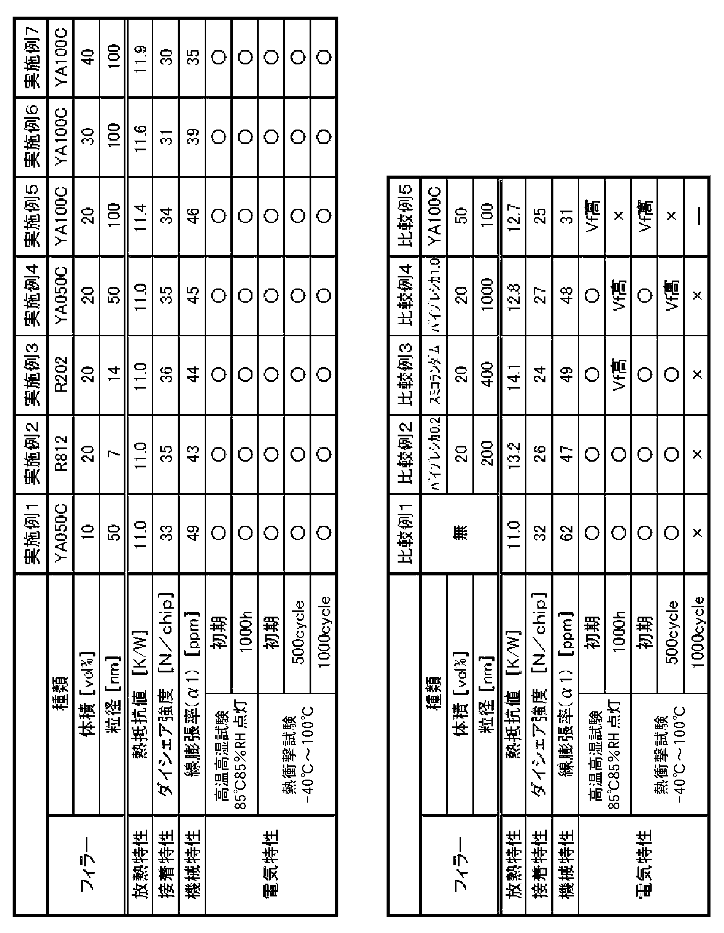
また、図5は、フィラー粒径に対する熱抵抗値を示すグラフである。このグラフより、フィラー粒径を100nm以下とすることにより、熱抵抗値を低下させることが可能であることがわかる。
実施例1からわかるように、バインダー樹脂に対して50nmのフィラーを10vol%添加したACPを用いたLED実装サンプルの熱抵抗値は11.0(K/W)で、フィラーを添加していない比較例1と同等の放熱性を維持した。また、ダイシェア強度は33N/chipで比較例1よりも向上した。線膨張係数は49ppmで比較例1よりも低線膨張化できた。さらに、85℃85%RH環境下での点灯試験では試験1000hにおいて電気接続信頼性も良好であった。また、熱衝撃試験500サイクル、1000サイクル経過後でも良好な電気接続信頼性が得られた。
実施例2からわかるように、バインダー樹脂に対して7nmのフィラーを20vol%添加したACPを用いたLED実装サンプルの熱抵抗値は11.0(K/W)で、比較例1と同等の放熱性を維持した。また、ダイシェア強度は35N/chipで比較例1よりも向上した。線膨張係数は43ppmで比較例1よりも低線膨張化できた。さらに、85℃85%RH環境下での点灯試験では試験1000hにおいて電気接続信頼性も良好であった。また、熱衝撃試験500サイクル、1000サイクル経過後でも良好な電気接続信頼性が得られた。
実施例3からわかるように、バインダー樹脂に対して14nmのフィラーを20vol%添加したACPを用いたLED実装サンプルの熱抵抗値は11.0(K/W)で、比較例1と同等の放熱性を維持した。また、ダイシェア強度は36N/chipで比較例1よりも向上した。線膨張係数は44ppmで比較例1よりも低線膨張化できた。さらに、85℃85%RH環境下での点灯試験では試験1000hにおいて電気接続信頼性も良好であった。また、熱衝撃試験500サイクル、1000サイクル経過後でも良好な電気接続信頼性が得られた。
実施例4からわかるように、バインダー樹脂に対して50nmのフィラーを20vol%添加したACPを用いたLED実装サンプルの熱抵抗値は11.0(K/W)で、比較例1と同等の放熱性を維持した。また、ダイシェア強度は35N/chipで比較例1よりも向上した。線膨張係数は45ppmで比較例1よりも低線膨張化できた。さらに、85℃85%RH環境下での点灯試験では試験1000hにおいて電気接続信頼性も良好であった。また、熱衝撃試験500サイクル、1000サイクル経過後でも良好な電気接続信頼性が得られた。
実施例5からわかるように、バインダー樹脂に対して100nmのフィラーを20vol%添加したACPを用いたLED実装サンプルの熱抵抗値は11.4(K/W)で、比較例1と同等の放熱性を維持した。また、ダイシェア強度は34N/chipで比較例1よりも向上した。線膨張係数は46ppmで比較例1よりも低線膨張化できた。さらに、85℃85%RH環境下での点灯試験では試験1000hにおいて電気接続信頼性も良好であった。また、熱衝撃試験500サイクル、1000サイクル経過後でも良好な電気接続信頼性が得られた。
実施例6からわかるように、バインダー樹脂に対して100nmのフィラーを30vol%添加したACPを用いたLED実装サンプルの熱抵抗値は11.6(K/W)で、比較例1と同等の放熱性を維持した。また、ダイシェア強度は31N/chipで比較例1と同等の接着強度を維持した。線膨張係数は39ppmで比較例1よりも低線膨張化できた。さらに、85℃85%RH環境下での点灯試験では試験1000hにおいて電気接続信頼性も良好であった。また、熱衝撃試験500サイクル、1000サイクル経過後でも良好な電気接続信頼性が得られた。
実施例7からわかるように、バインダー樹脂に対して100nmのフィラーを40vol%添加したACPを用いたLED実装サンプルの熱抵抗値は11.9(K/W)で、比較例1と同等の放熱性を維持した。また、ダイシェア強度は30N/chipで比較例1と同等の接着強度を維持した。線膨張係数は35ppmで比較例1よりも低線膨張化できた。さらに、85℃85%RH環境下での点灯試験では試験1000hにおいて電気接続信頼性も良好であった。また、熱衝撃試験500サイクル、1000サイクル経過後でも良好な電気接続信頼性が得られた。
比較例1からわかるように、バインダー樹脂に対してフィラーを配合していないACPを用いたLED実装サンプルの熱抵抗値は11.0(K/W)であった。また、ダイシェア強度は32N/chipであった。線膨張係数は62ppmであった。さらに、85℃85%RH環境下での点灯試験では試験1000hにおいて電気接続信頼性も良好であった。また、熱衝撃試験500サイクル経過後で良好な電気接続信頼性を得られたが、1000サイクル経過後においてOPENが発生したため良好な電気接続信頼性が得られなかった。
比較例2からわかるように、バインダー樹脂に対して200nmのフィラーを20vol%添加したACPを用いたLED実装サンプルでは、図6に示すように、フィラーの噛み込みが発生し、熱抵抗値は13.2(K/W)で、比較例1よりも放熱性が悪化した。図6のようにフィラーが噛み込まれると、はんだ接合が十分ではなく、熱抵抗率の悪化と接続信頼性が悪化する。また、ダイシェア強度は26N/chipで比較例1よりも悪化した。線膨張係数は47ppmで比較例1よりも低線膨張化できた。85℃85%RH環境下での点灯試験では試験1000hにおいて電気接続信頼性も良好であった。また、熱衝撃試験500サイクル経過後で良好な電気接続信頼性を得られたが、1000サイクル経過後においてOPENが発生したため良好な電気接続信頼性が得られなかった。
比較例3からわかるように、バインダー樹脂に対して400nmのフィラーを20vol%添加したACPを用いたLED実装サンプルでは、フィラーの噛み込みが発生し、熱抵抗値は14.1(K/W)で、比較例1よりも放熱性が悪化した。また、ダイシェア強度は24N/chipで比較例1よりも悪化した。線膨張係数は49ppmで比較例1よりも低線膨張化できた。85℃85%RH環境下での点灯試験では初期の電気特性は良好であったが、試験1000hにおいてVf値の上昇が確認された。また、熱衝撃試験500サイクル経過後で良好な電気接続信頼性を得られたが、1000サイクル経過後においてOPENが発生したため良好な電気接続信頼性が得られなかった。
比較例4からわかるように、バインダー樹脂に対して1000nmのフィラーを20vol%添加したACPを用いたLED実装サンプルでは、フィラーの噛み込みが発生し、熱抵抗値は12.8(K/W)で、比較例1よりも放熱性が悪化した。また、ダイシェア強度は27N/chipで比較例1よりも悪化した。線膨張係数は48ppmで比較例1よりも低線膨張化できた。85℃85%RH環境下での点灯試験では初期の電気特性は良好であったが、試験1000hにおいてVf値の上昇が確認された。また、熱衝撃試験500サイクル経過後でVfの上昇が確認された。さらに、1000サイクル経過後でOPENが発生したため良好な電気接続信頼性が得られなかった。
比較例5からわかるように、バインダー樹脂に対して100nmのフィラーを50vol%添加したACPを用いたLED実装サンプルでは、フィラーの噛み込みが発生し、熱抵抗値は12.7(K/W)で、比較例1よりも放熱性が悪化した。また、ダイシェア強度は25N/chipで比較例1よりも悪化した。線膨張係数は31ppmで比較例1よりも低線膨張化できた。また、初期からVf値が高く、85℃85%RH環境下での点灯試験1000h、熱衝撃試験500サイクル経過後でOPENが発生したため良好な電気接続信頼性が得られなかった。
以上のように、はんだ粒子と導電性粒子を併用した異方性導電接着剤に100nm以下のフィラーを配合することで、LEDパッケージの放熱性・接着特性へ悪影響を与えることなく、低線膨張化することができた。
1…LED実装体(接続構造体) 2、3…端子 10…LED素子(第1の電子部品) 11…素子基板、12…第1導電型クラッド層、12a…第1導電型電極(端子)、13…活性層、14…第2導電型クラッド層、14a…第2導電型電極(端子)、15…パッシベーション、20…基板(第2の電子部品)、21…基材、22…第1導電型用回路パターン、23…第2導電型用回路パターン、30…異方性導電接着剤、31…導電性粒子、32…はんだ粒子、33…バインダー(接着剤成分)、34…無機充填材、101…素子基板、102…第1導電型クラッド層、103…活性層、104…第2導電型クラッド層、105…パッシベーション、201…基材、202…第1導電型用回路パターン、203…第2導電型用回路パターン、301a、301b…ボンディングワイヤ、302…ダイボンド材、303…はんだペースト、304…封止樹脂、305…バインダー、306…導電性粒子、307…電極接続部
Claims (8)
- 樹脂粒子の表面に導電性金属層が形成され、平均粒径が1~10μmである導電性粒子と、
平均粒径が前記導電性粒子の平均粒径の25~400%であるはんだ粒子と、
平均粒径が100nm以下である無機充填材と
が接着剤成分に分散されてなる異方性導電接着剤。 - 前記無機充填材の配合量が、10~40vol%である請求項1記載の異方性導電接着剤。
- 前記導電性粒子の配合量が、1~30vol%であり、
前記はんだ粒子の配合量が、1~30vol%である請求項2記載の異方性導電接着剤。 - 前記接着剤成分が、エポキシ化合物と、酸無水物とを含有する請求項1記載の異方性導電接着剤。
- 線膨張係数が、50ppm以下である請求項1記載の異方性導電接着剤。
- 第1の電子部品の端子と、第2の電子部品の端子とが、樹脂粒子の表面に導電性金属層が形成された導電性粒子と、はんだ粒子と、無機充填材とを含有する異方性導電接着剤を介して電気的に接続されてなり、
前記第1の電子部品の端子と前記第2の電子部品の端子とが、前記導電性粒子により接続されるともに、前記はんだ粒子によりはんだ接合されてなり、
前記無機充填材の平均粒径が、100nm以下である接続構造体。 - 前記第1の電子部品が、LED素子であり、
前記第2の電子部品が、アルミベースのMCPCB基板である請求項6記載の接続構造体。 - 前記異方性導電接着剤の線膨張係数が、50ppm以下であり、
熱抵抗値が、12K/W以下である請求項6又は7のいずれか1項記載の接続構造体。
Applications Claiming Priority (2)
| Application Number | Priority Date | Filing Date | Title |
|---|---|---|---|
| JP2013216239 | 2013-10-17 | ||
| JP2013-216239 | 2013-10-17 |
Publications (1)
| Publication Number | Publication Date |
|---|---|
| WO2015056754A1 true WO2015056754A1 (ja) | 2015-04-23 |
Family
ID=52828195
Family Applications (1)
| Application Number | Title | Priority Date | Filing Date |
|---|---|---|---|
| PCT/JP2014/077598 Ceased WO2015056754A1 (ja) | 2013-10-17 | 2014-10-16 | 異方性導電接着剤及び接続構造体 |
Country Status (3)
| Country | Link |
|---|---|
| JP (1) | JP2015098588A (ja) |
| TW (1) | TW201533212A (ja) |
| WO (1) | WO2015056754A1 (ja) |
Cited By (2)
| Publication number | Priority date | Publication date | Assignee | Title |
|---|---|---|---|---|
| CN112531093A (zh) * | 2020-05-26 | 2021-03-19 | 友达光电股份有限公司 | 发光装置及其制造方法 |
| JP2021068842A (ja) * | 2019-10-25 | 2021-04-30 | デクセリアルズ株式会社 | 接続体の製造方法、異方性導電接合材料、及び接続体 |
Families Citing this family (7)
| Publication number | Priority date | Publication date | Assignee | Title |
|---|---|---|---|---|
| KR102605942B1 (ko) * | 2015-08-24 | 2023-11-27 | 세키스이가가쿠 고교가부시키가이샤 | 도전 재료 및 접속 구조체 |
| JP6519407B2 (ja) * | 2015-08-26 | 2019-05-29 | 日亜化学工業株式会社 | 発光装置及び発光装置の製造方法 |
| JP2017122144A (ja) * | 2016-01-05 | 2017-07-13 | デクセリアルズ株式会社 | 接着剤組成物 |
| KR102428039B1 (ko) * | 2016-10-06 | 2022-08-03 | 세키스이가가쿠 고교가부시키가이샤 | 도전 재료, 접속 구조체 및 접속 구조체의 제조 방법 |
| JP2018088498A (ja) * | 2016-11-29 | 2018-06-07 | デクセリアルズ株式会社 | 異方性導電接着剤 |
| JP2021103608A (ja) * | 2019-12-24 | 2021-07-15 | デクセリアルズ株式会社 | 異方性導電接着剤 |
| WO2023182046A1 (ja) * | 2022-03-22 | 2023-09-28 | デクセリアルズ株式会社 | エステル化合物及びその製造方法、並びに熱伝導性組成物及び熱伝導性シート |
Citations (15)
| Publication number | Priority date | Publication date | Assignee | Title |
|---|---|---|---|---|
| JPS6459786A (en) * | 1987-08-31 | 1989-03-07 | Hitachi Chemical Co Ltd | Connection member of circuit |
| JPH03129607A (ja) * | 1989-10-14 | 1991-06-03 | Sony Chem Corp | 異方性導電膜 |
| JPH04180029A (ja) * | 1990-11-15 | 1992-06-26 | Seiko Epson Corp | 回路の接続構造体 |
| JPH06187834A (ja) * | 1992-12-18 | 1994-07-08 | Sumitomo Bakelite Co Ltd | 異方導電フィルム |
| WO2001071854A1 (fr) * | 2000-03-23 | 2001-09-27 | Sony Corporation | Materiau pour connexion electrique et procede de connexion electrique |
| JP2006108523A (ja) * | 2004-10-08 | 2006-04-20 | Hitachi Chem Co Ltd | 異方性導電フィルムを用いた電気部品の接続方法 |
| JP2007049045A (ja) * | 2005-08-11 | 2007-02-22 | Rohm Co Ltd | 半導体発光素子およびこれを備えた半導体装置 |
| JP2007324417A (ja) * | 2006-06-01 | 2007-12-13 | Sharp Corp | 半導体発光装置とその製造方法 |
| JP2008072038A (ja) * | 2006-09-15 | 2008-03-27 | Matsushita Electric Ind Co Ltd | 電気部品の接続方法 |
| WO2008123087A1 (ja) * | 2007-03-19 | 2008-10-16 | Namics Coropration | 異方性導電ペースト |
| JP2010287836A (ja) * | 2009-06-15 | 2010-12-24 | Hitachi Chem Co Ltd | 半導体加工用接着フィルム積層体 |
| JP2011036901A (ja) * | 2009-08-17 | 2011-02-24 | Tamura Seisakusho Co Ltd | はんだ接合剤組成物 |
| JP2013118181A (ja) * | 2011-11-02 | 2013-06-13 | Sekisui Chem Co Ltd | 異方性導電材料及び接続構造体 |
| JP2013118180A (ja) * | 2011-11-02 | 2013-06-13 | Sekisui Chem Co Ltd | 異方性導電材料及び接続構造体 |
| WO2014046093A1 (ja) * | 2012-09-24 | 2014-03-27 | デクセリアルズ株式会社 | 異方性導電接着剤 |
-
2014
- 2014-10-16 WO PCT/JP2014/077598 patent/WO2015056754A1/ja not_active Ceased
- 2014-10-16 JP JP2014212018A patent/JP2015098588A/ja active Pending
- 2014-10-17 TW TW103135951A patent/TW201533212A/zh unknown
Patent Citations (15)
| Publication number | Priority date | Publication date | Assignee | Title |
|---|---|---|---|---|
| JPS6459786A (en) * | 1987-08-31 | 1989-03-07 | Hitachi Chemical Co Ltd | Connection member of circuit |
| JPH03129607A (ja) * | 1989-10-14 | 1991-06-03 | Sony Chem Corp | 異方性導電膜 |
| JPH04180029A (ja) * | 1990-11-15 | 1992-06-26 | Seiko Epson Corp | 回路の接続構造体 |
| JPH06187834A (ja) * | 1992-12-18 | 1994-07-08 | Sumitomo Bakelite Co Ltd | 異方導電フィルム |
| WO2001071854A1 (fr) * | 2000-03-23 | 2001-09-27 | Sony Corporation | Materiau pour connexion electrique et procede de connexion electrique |
| JP2006108523A (ja) * | 2004-10-08 | 2006-04-20 | Hitachi Chem Co Ltd | 異方性導電フィルムを用いた電気部品の接続方法 |
| JP2007049045A (ja) * | 2005-08-11 | 2007-02-22 | Rohm Co Ltd | 半導体発光素子およびこれを備えた半導体装置 |
| JP2007324417A (ja) * | 2006-06-01 | 2007-12-13 | Sharp Corp | 半導体発光装置とその製造方法 |
| JP2008072038A (ja) * | 2006-09-15 | 2008-03-27 | Matsushita Electric Ind Co Ltd | 電気部品の接続方法 |
| WO2008123087A1 (ja) * | 2007-03-19 | 2008-10-16 | Namics Coropration | 異方性導電ペースト |
| JP2010287836A (ja) * | 2009-06-15 | 2010-12-24 | Hitachi Chem Co Ltd | 半導体加工用接着フィルム積層体 |
| JP2011036901A (ja) * | 2009-08-17 | 2011-02-24 | Tamura Seisakusho Co Ltd | はんだ接合剤組成物 |
| JP2013118181A (ja) * | 2011-11-02 | 2013-06-13 | Sekisui Chem Co Ltd | 異方性導電材料及び接続構造体 |
| JP2013118180A (ja) * | 2011-11-02 | 2013-06-13 | Sekisui Chem Co Ltd | 異方性導電材料及び接続構造体 |
| WO2014046093A1 (ja) * | 2012-09-24 | 2014-03-27 | デクセリアルズ株式会社 | 異方性導電接着剤 |
Cited By (4)
| Publication number | Priority date | Publication date | Assignee | Title |
|---|---|---|---|---|
| JP2021068842A (ja) * | 2019-10-25 | 2021-04-30 | デクセリアルズ株式会社 | 接続体の製造方法、異方性導電接合材料、及び接続体 |
| JP7032367B2 (ja) | 2019-10-25 | 2022-03-08 | デクセリアルズ株式会社 | 接続体の製造方法、異方性導電接合材料、及び接続体 |
| CN112531093A (zh) * | 2020-05-26 | 2021-03-19 | 友达光电股份有限公司 | 发光装置及其制造方法 |
| CN112531093B (zh) * | 2020-05-26 | 2023-08-15 | 友达光电股份有限公司 | 发光装置及其制造方法 |
Also Published As
| Publication number | Publication date |
|---|---|
| TW201533212A (zh) | 2015-09-01 |
| JP2015098588A (ja) | 2015-05-28 |
Similar Documents
| Publication | Publication Date | Title |
|---|---|---|
| KR102159992B1 (ko) | 이방성 도전 접착제 | |
| JP6066643B2 (ja) | 異方性導電接着剤 | |
| WO2015056754A1 (ja) | 異方性導電接着剤及び接続構造体 | |
| JP6176910B2 (ja) | 接続構造体の製造方法 | |
| JP6347635B2 (ja) | 異方性導電接着剤 | |
| WO2015046326A1 (ja) | 発光装置、異方性導電接着剤、発光装置製造方法 | |
| KR102368748B1 (ko) | 접착제 및 접속 구조체 | |
| TWI669721B (zh) | Anisotropic conductive adhesive | |
| JP6430148B2 (ja) | 接着剤及び接続構造体 | |
| JP2014065765A (ja) | 異方性導電接着剤 | |
| WO2021131586A1 (ja) | 異方性導電接着剤 |
Legal Events
| Date | Code | Title | Description |
|---|---|---|---|
| 121 | Ep: the epo has been informed by wipo that ep was designated in this application |
Ref document number: 14854524 Country of ref document: EP Kind code of ref document: A1 |
|
| NENP | Non-entry into the national phase |
Ref country code: DE |
|
| 122 | Ep: pct application non-entry in european phase |
Ref document number: 14854524 Country of ref document: EP Kind code of ref document: A1 |