WO2015056512A1 - 電気接続材料 - Google Patents
電気接続材料 Download PDFInfo
- Publication number
- WO2015056512A1 WO2015056512A1 PCT/JP2014/074510 JP2014074510W WO2015056512A1 WO 2015056512 A1 WO2015056512 A1 WO 2015056512A1 JP 2014074510 W JP2014074510 W JP 2014074510W WO 2015056512 A1 WO2015056512 A1 WO 2015056512A1
- Authority
- WO
- WIPO (PCT)
- Prior art keywords
- resin composition
- polymerizable compound
- polymerization initiator
- composition layer
- epoxy
- Prior art date
- Legal status (The legal status is an assumption and is not a legal conclusion. Google has not performed a legal analysis and makes no representation as to the accuracy of the status listed.)
- Ceased
Links
Images
Classifications
-
- H—ELECTRICITY
- H01—ELECTRIC ELEMENTS
- H01B—CABLES; CONDUCTORS; INSULATORS; SELECTION OF MATERIALS FOR THEIR CONDUCTIVE, INSULATING OR DIELECTRIC PROPERTIES
- H01B5/00—Non-insulated conductors or conductive bodies characterised by their form
- H01B5/14—Non-insulated conductors or conductive bodies characterised by their form comprising conductive layers or films on insulating-supports
-
- C—CHEMISTRY; METALLURGY
- C08—ORGANIC MACROMOLECULAR COMPOUNDS; THEIR PREPARATION OR CHEMICAL WORKING-UP; COMPOSITIONS BASED THEREON
- C08F—MACROMOLECULAR COMPOUNDS OBTAINED BY REACTIONS ONLY INVOLVING CARBON-TO-CARBON UNSATURATED BONDS
- C08F2/00—Processes of polymerisation
- C08F2/44—Polymerisation in the presence of compounding ingredients, e.g. plasticisers, dyestuffs, fillers
-
- C—CHEMISTRY; METALLURGY
- C08—ORGANIC MACROMOLECULAR COMPOUNDS; THEIR PREPARATION OR CHEMICAL WORKING-UP; COMPOSITIONS BASED THEREON
- C08F—MACROMOLECULAR COMPOUNDS OBTAINED BY REACTIONS ONLY INVOLVING CARBON-TO-CARBON UNSATURATED BONDS
- C08F2/00—Processes of polymerisation
- C08F2/46—Polymerisation initiated by wave energy or particle radiation
- C08F2/48—Polymerisation initiated by wave energy or particle radiation by ultraviolet or visible light
-
- C—CHEMISTRY; METALLURGY
- C09—DYES; PAINTS; POLISHES; NATURAL RESINS; ADHESIVES; COMPOSITIONS NOT OTHERWISE PROVIDED FOR; APPLICATIONS OF MATERIALS NOT OTHERWISE PROVIDED FOR
- C09J—ADHESIVES; NON-MECHANICAL ASPECTS OF ADHESIVE PROCESSES IN GENERAL; ADHESIVE PROCESSES NOT PROVIDED FOR ELSEWHERE; USE OF MATERIALS AS ADHESIVES
- C09J163/00—Adhesives based on epoxy resins; Adhesives based on derivatives of epoxy resins
-
- C—CHEMISTRY; METALLURGY
- C09—DYES; PAINTS; POLISHES; NATURAL RESINS; ADHESIVES; COMPOSITIONS NOT OTHERWISE PROVIDED FOR; APPLICATIONS OF MATERIALS NOT OTHERWISE PROVIDED FOR
- C09J—ADHESIVES; NON-MECHANICAL ASPECTS OF ADHESIVE PROCESSES IN GENERAL; ADHESIVE PROCESSES NOT PROVIDED FOR ELSEWHERE; USE OF MATERIALS AS ADHESIVES
- C09J201/00—Adhesives based on unspecified macromolecular compounds
-
- H—ELECTRICITY
- H01—ELECTRIC ELEMENTS
- H01B—CABLES; CONDUCTORS; INSULATORS; SELECTION OF MATERIALS FOR THEIR CONDUCTIVE, INSULATING OR DIELECTRIC PROPERTIES
- H01B1/00—Conductors or conductive bodies characterised by the conductive materials; Selection of materials as conductors
- H01B1/20—Conductive material dispersed in non-conductive organic material
-
- H—ELECTRICITY
- H01—ELECTRIC ELEMENTS
- H01B—CABLES; CONDUCTORS; INSULATORS; SELECTION OF MATERIALS FOR THEIR CONDUCTIVE, INSULATING OR DIELECTRIC PROPERTIES
- H01B1/00—Conductors or conductive bodies characterised by the conductive materials; Selection of materials as conductors
- H01B1/20—Conductive material dispersed in non-conductive organic material
- H01B1/22—Conductive material dispersed in non-conductive organic material the conductive material comprising metals or alloys
-
- H—ELECTRICITY
- H01—ELECTRIC ELEMENTS
- H01B—CABLES; CONDUCTORS; INSULATORS; SELECTION OF MATERIALS FOR THEIR CONDUCTIVE, INSULATING OR DIELECTRIC PROPERTIES
- H01B13/00—Apparatus or processes specially adapted for manufacturing conductors or cables
- H01B13/0026—Apparatus for manufacturing conducting or semi-conducting layers, e.g. deposition of metal
-
- H—ELECTRICITY
- H01—ELECTRIC ELEMENTS
- H01B—CABLES; CONDUCTORS; INSULATORS; SELECTION OF MATERIALS FOR THEIR CONDUCTIVE, INSULATING OR DIELECTRIC PROPERTIES
- H01B3/00—Insulators or insulating bodies characterised by the insulating materials; Selection of materials for their insulating or dielectric properties
- H01B3/18—Insulators or insulating bodies characterised by the insulating materials; Selection of materials for their insulating or dielectric properties mainly consisting of organic substances
- H01B3/30—Insulators or insulating bodies characterised by the insulating materials; Selection of materials for their insulating or dielectric properties mainly consisting of organic substances plastics; resins; waxes
- H01B3/40—Insulators or insulating bodies characterised by the insulating materials; Selection of materials for their insulating or dielectric properties mainly consisting of organic substances plastics; resins; waxes epoxy resins
-
- H—ELECTRICITY
- H01—ELECTRIC ELEMENTS
- H01R—ELECTRICALLY-CONDUCTIVE CONNECTIONS; STRUCTURAL ASSOCIATIONS OF A PLURALITY OF MUTUALLY-INSULATED ELECTRICAL CONNECTING ELEMENTS; COUPLING DEVICES; CURRENT COLLECTORS
- H01R4/00—Electrically-conductive connections between two or more conductive members in direct contact, i.e. touching one another; Means for effecting or maintaining such contact; Electrically-conductive connections having two or more spaced connecting locations for conductors and using contact members penetrating insulation
- H01R4/04—Electrically-conductive connections between two or more conductive members in direct contact, i.e. touching one another; Means for effecting or maintaining such contact; Electrically-conductive connections having two or more spaced connecting locations for conductors and using contact members penetrating insulation using electrically conductive adhesives
-
- H—ELECTRICITY
- H05—ELECTRIC TECHNIQUES NOT OTHERWISE PROVIDED FOR
- H05K—PRINTED CIRCUITS; CASINGS OR CONSTRUCTIONAL DETAILS OF ELECTRIC APPARATUS; MANUFACTURE OF ASSEMBLAGES OF ELECTRICAL COMPONENTS
- H05K1/00—Printed circuits
- H05K1/02—Details
- H05K1/03—Use of materials for the substrate
- H05K1/0313—Organic insulating material
- H05K1/0353—Organic insulating material consisting of two or more materials, e.g. two or more polymers, polymer + filler, + reinforcement
-
- H—ELECTRICITY
- H05—ELECTRIC TECHNIQUES NOT OTHERWISE PROVIDED FOR
- H05K—PRINTED CIRCUITS; CASINGS OR CONSTRUCTIONAL DETAILS OF ELECTRIC APPARATUS; MANUFACTURE OF ASSEMBLAGES OF ELECTRICAL COMPONENTS
- H05K1/00—Printed circuits
- H05K1/02—Details
- H05K1/09—Use of materials for the conductive, e.g. metallic pattern
-
- H—ELECTRICITY
- H05—ELECTRIC TECHNIQUES NOT OTHERWISE PROVIDED FOR
- H05K—PRINTED CIRCUITS; CASINGS OR CONSTRUCTIONAL DETAILS OF ELECTRIC APPARATUS; MANUFACTURE OF ASSEMBLAGES OF ELECTRICAL COMPONENTS
- H05K1/00—Printed circuits
- H05K1/18—Printed circuits structurally associated with non-printed electric components
-
- H—ELECTRICITY
- H05—ELECTRIC TECHNIQUES NOT OTHERWISE PROVIDED FOR
- H05K—PRINTED CIRCUITS; CASINGS OR CONSTRUCTIONAL DETAILS OF ELECTRIC APPARATUS; MANUFACTURE OF ASSEMBLAGES OF ELECTRICAL COMPONENTS
- H05K3/00—Apparatus or processes for manufacturing printed circuits
- H05K3/02—Apparatus or processes for manufacturing printed circuits in which the conductive material is applied to the surface of the insulating support and is thereafter removed from such areas of the surface which are not intended for current conducting or shielding
- H05K3/06—Apparatus or processes for manufacturing printed circuits in which the conductive material is applied to the surface of the insulating support and is thereafter removed from such areas of the surface which are not intended for current conducting or shielding the conductive material being removed chemically or electrolytically, e.g. by photo-etch process
-
- H—ELECTRICITY
- H01—ELECTRIC ELEMENTS
- H01R—ELECTRICALLY-CONDUCTIVE CONNECTIONS; STRUCTURAL ASSOCIATIONS OF A PLURALITY OF MUTUALLY-INSULATED ELECTRICAL CONNECTING ELEMENTS; COUPLING DEVICES; CURRENT COLLECTORS
- H01R12/00—Structural associations of a plurality of mutually-insulated electrical connecting elements, specially adapted for printed circuits, e.g. printed circuit boards [PCB], flat or ribbon cables, or like generally planar structures, e.g. terminal strips, terminal blocks; Coupling devices specially adapted for printed circuits, flat or ribbon cables, or like generally planar structures; Terminals specially adapted for contact with, or insertion into, printed circuits, flat or ribbon cables, or like generally planar structures
- H01R12/50—Fixed connections
- H01R12/51—Fixed connections for rigid printed circuits or like structures
- H01R12/55—Fixed connections for rigid printed circuits or like structures characterised by the terminals
- H01R12/57—Fixed connections for rigid printed circuits or like structures characterised by the terminals surface mounting terminals
-
- H—ELECTRICITY
- H05—ELECTRIC TECHNIQUES NOT OTHERWISE PROVIDED FOR
- H05K—PRINTED CIRCUITS; CASINGS OR CONSTRUCTIONAL DETAILS OF ELECTRIC APPARATUS; MANUFACTURE OF ASSEMBLAGES OF ELECTRICAL COMPONENTS
- H05K3/00—Apparatus or processes for manufacturing printed circuits
- H05K3/30—Assembling printed circuits with electric components, e.g. with resistors
- H05K3/32—Assembling printed circuits with electric components, e.g. with resistors electrically connecting electric components or wires to printed circuits
- H05K3/321—Assembling printed circuits with electric components, e.g. with resistors electrically connecting electric components or wires to printed circuits by conductive adhesives
- H05K3/323—Assembling printed circuits with electric components, e.g. with resistors electrically connecting electric components or wires to printed circuits by conductive adhesives by applying an anisotropic conductive adhesive layer over an array of pads
-
- H—ELECTRICITY
- H10—SEMICONDUCTOR DEVICES; ELECTRIC SOLID-STATE DEVICES NOT OTHERWISE PROVIDED FOR
- H10W—GENERIC PACKAGES, INTERCONNECTIONS, CONNECTORS OR OTHER CONSTRUCTIONAL DETAILS OF DEVICES COVERED BY CLASS H10
- H10W72/00—Interconnections or connectors in packages
- H10W72/01—Manufacture or treatment
- H10W72/013—Manufacture or treatment of die-attach connectors
- H10W72/01304—Manufacture or treatment of die-attach connectors using temporary auxiliary members, e.g. using sacrificial coatings or handle substrates
-
- H—ELECTRICITY
- H10—SEMICONDUCTOR DEVICES; ELECTRIC SOLID-STATE DEVICES NOT OTHERWISE PROVIDED FOR
- H10W—GENERIC PACKAGES, INTERCONNECTIONS, CONNECTORS OR OTHER CONSTRUCTIONAL DETAILS OF DEVICES COVERED BY CLASS H10
- H10W72/00—Interconnections or connectors in packages
- H10W72/01—Manufacture or treatment
- H10W72/013—Manufacture or treatment of die-attach connectors
- H10W72/01315—Forming coatings
-
- H—ELECTRICITY
- H10—SEMICONDUCTOR DEVICES; ELECTRIC SOLID-STATE DEVICES NOT OTHERWISE PROVIDED FOR
- H10W—GENERIC PACKAGES, INTERCONNECTIONS, CONNECTORS OR OTHER CONSTRUCTIONAL DETAILS OF DEVICES COVERED BY CLASS H10
- H10W72/00—Interconnections or connectors in packages
- H10W72/01—Manufacture or treatment
- H10W72/013—Manufacture or treatment of die-attach connectors
- H10W72/01321—Manufacture or treatment of die-attach connectors using local deposition
- H10W72/01323—Manufacture or treatment of die-attach connectors using local deposition in liquid form, e.g. by dispensing droplets or by screen printing
-
- H—ELECTRICITY
- H10—SEMICONDUCTOR DEVICES; ELECTRIC SOLID-STATE DEVICES NOT OTHERWISE PROVIDED FOR
- H10W—GENERIC PACKAGES, INTERCONNECTIONS, CONNECTORS OR OTHER CONSTRUCTIONAL DETAILS OF DEVICES COVERED BY CLASS H10
- H10W72/00—Interconnections or connectors in packages
- H10W72/071—Connecting or disconnecting
- H10W72/072—Connecting or disconnecting of bump connectors
-
- H—ELECTRICITY
- H10—SEMICONDUCTOR DEVICES; ELECTRIC SOLID-STATE DEVICES NOT OTHERWISE PROVIDED FOR
- H10W—GENERIC PACKAGES, INTERCONNECTIONS, CONNECTORS OR OTHER CONSTRUCTIONAL DETAILS OF DEVICES COVERED BY CLASS H10
- H10W72/00—Interconnections or connectors in packages
- H10W72/071—Connecting or disconnecting
- H10W72/073—Connecting or disconnecting of die-attach connectors
-
- H—ELECTRICITY
- H10—SEMICONDUCTOR DEVICES; ELECTRIC SOLID-STATE DEVICES NOT OTHERWISE PROVIDED FOR
- H10W—GENERIC PACKAGES, INTERCONNECTIONS, CONNECTORS OR OTHER CONSTRUCTIONAL DETAILS OF DEVICES COVERED BY CLASS H10
- H10W72/00—Interconnections or connectors in packages
- H10W72/071—Connecting or disconnecting
- H10W72/073—Connecting or disconnecting of die-attach connectors
- H10W72/07331—Connecting techniques
- H10W72/07332—Compression bonding, e.g. thermocompression bonding
-
- H—ELECTRICITY
- H10—SEMICONDUCTOR DEVICES; ELECTRIC SOLID-STATE DEVICES NOT OTHERWISE PROVIDED FOR
- H10W—GENERIC PACKAGES, INTERCONNECTIONS, CONNECTORS OR OTHER CONSTRUCTIONAL DETAILS OF DEVICES COVERED BY CLASS H10
- H10W72/00—Interconnections or connectors in packages
- H10W72/071—Connecting or disconnecting
- H10W72/073—Connecting or disconnecting of die-attach connectors
- H10W72/07331—Connecting techniques
- H10W72/07337—Connecting techniques using a polymer adhesive, e.g. an adhesive based on silicone or epoxy
- H10W72/07338—Connecting techniques using a polymer adhesive, e.g. an adhesive based on silicone or epoxy hardening the adhesive by curing, e.g. thermosetting
-
- H—ELECTRICITY
- H10—SEMICONDUCTOR DEVICES; ELECTRIC SOLID-STATE DEVICES NOT OTHERWISE PROVIDED FOR
- H10W—GENERIC PACKAGES, INTERCONNECTIONS, CONNECTORS OR OTHER CONSTRUCTIONAL DETAILS OF DEVICES COVERED BY CLASS H10
- H10W72/00—Interconnections or connectors in packages
- H10W72/071—Connecting or disconnecting
- H10W72/074—Connecting or disconnecting of anisotropic conductive adhesives
-
- H—ELECTRICITY
- H10—SEMICONDUCTOR DEVICES; ELECTRIC SOLID-STATE DEVICES NOT OTHERWISE PROVIDED FOR
- H10W—GENERIC PACKAGES, INTERCONNECTIONS, CONNECTORS OR OTHER CONSTRUCTIONAL DETAILS OF DEVICES COVERED BY CLASS H10
- H10W72/00—Interconnections or connectors in packages
- H10W72/20—Bump connectors, e.g. solder bumps or copper pillars; Dummy bumps; Thermal bumps
- H10W72/241—Dispositions, e.g. layouts
-
- H—ELECTRICITY
- H10—SEMICONDUCTOR DEVICES; ELECTRIC SOLID-STATE DEVICES NOT OTHERWISE PROVIDED FOR
- H10W—GENERIC PACKAGES, INTERCONNECTIONS, CONNECTORS OR OTHER CONSTRUCTIONAL DETAILS OF DEVICES COVERED BY CLASS H10
- H10W72/00—Interconnections or connectors in packages
- H10W72/20—Bump connectors, e.g. solder bumps or copper pillars; Dummy bumps; Thermal bumps
- H10W72/251—Materials
- H10W72/252—Materials comprising solid metals or solid metalloids, e.g. PbSn, Ag or Cu
-
- H—ELECTRICITY
- H10—SEMICONDUCTOR DEVICES; ELECTRIC SOLID-STATE DEVICES NOT OTHERWISE PROVIDED FOR
- H10W—GENERIC PACKAGES, INTERCONNECTIONS, CONNECTORS OR OTHER CONSTRUCTIONAL DETAILS OF DEVICES COVERED BY CLASS H10
- H10W72/00—Interconnections or connectors in packages
- H10W72/20—Bump connectors, e.g. solder bumps or copper pillars; Dummy bumps; Thermal bumps
- H10W72/261—Functions other than electrical connecting
-
- H—ELECTRICITY
- H10—SEMICONDUCTOR DEVICES; ELECTRIC SOLID-STATE DEVICES NOT OTHERWISE PROVIDED FOR
- H10W—GENERIC PACKAGES, INTERCONNECTIONS, CONNECTORS OR OTHER CONSTRUCTIONAL DETAILS OF DEVICES COVERED BY CLASS H10
- H10W72/00—Interconnections or connectors in packages
- H10W72/30—Die-attach connectors
- H10W72/321—Structures or relative sizes of die-attach connectors
- H10W72/322—Multilayered die-attach connectors, e.g. a coating on a top surface of a core
-
- H—ELECTRICITY
- H10—SEMICONDUCTOR DEVICES; ELECTRIC SOLID-STATE DEVICES NOT OTHERWISE PROVIDED FOR
- H10W—GENERIC PACKAGES, INTERCONNECTIONS, CONNECTORS OR OTHER CONSTRUCTIONAL DETAILS OF DEVICES COVERED BY CLASS H10
- H10W72/00—Interconnections or connectors in packages
- H10W72/30—Die-attach connectors
- H10W72/321—Structures or relative sizes of die-attach connectors
- H10W72/325—Die-attach connectors having a filler embedded in a matrix
-
- H—ELECTRICITY
- H10—SEMICONDUCTOR DEVICES; ELECTRIC SOLID-STATE DEVICES NOT OTHERWISE PROVIDED FOR
- H10W—GENERIC PACKAGES, INTERCONNECTIONS, CONNECTORS OR OTHER CONSTRUCTIONAL DETAILS OF DEVICES COVERED BY CLASS H10
- H10W72/00—Interconnections or connectors in packages
- H10W72/30—Die-attach connectors
- H10W72/351—Materials of die-attach connectors
- H10W72/352—Materials of die-attach connectors comprising metals or metalloids, e.g. solders
-
- H—ELECTRICITY
- H10—SEMICONDUCTOR DEVICES; ELECTRIC SOLID-STATE DEVICES NOT OTHERWISE PROVIDED FOR
- H10W—GENERIC PACKAGES, INTERCONNECTIONS, CONNECTORS OR OTHER CONSTRUCTIONAL DETAILS OF DEVICES COVERED BY CLASS H10
- H10W72/00—Interconnections or connectors in packages
- H10W72/30—Die-attach connectors
- H10W72/351—Materials of die-attach connectors
- H10W72/353—Materials of die-attach connectors not comprising solid metals or solid metalloids, e.g. ceramics
-
- H—ELECTRICITY
- H10—SEMICONDUCTOR DEVICES; ELECTRIC SOLID-STATE DEVICES NOT OTHERWISE PROVIDED FOR
- H10W—GENERIC PACKAGES, INTERCONNECTIONS, CONNECTORS OR OTHER CONSTRUCTIONAL DETAILS OF DEVICES COVERED BY CLASS H10
- H10W72/00—Interconnections or connectors in packages
- H10W72/30—Die-attach connectors
- H10W72/351—Materials of die-attach connectors
- H10W72/353—Materials of die-attach connectors not comprising solid metals or solid metalloids, e.g. ceramics
- H10W72/354—Materials of die-attach connectors not comprising solid metals or solid metalloids, e.g. ceramics comprising polymers
-
- H—ELECTRICITY
- H10—SEMICONDUCTOR DEVICES; ELECTRIC SOLID-STATE DEVICES NOT OTHERWISE PROVIDED FOR
- H10W—GENERIC PACKAGES, INTERCONNECTIONS, CONNECTORS OR OTHER CONSTRUCTIONAL DETAILS OF DEVICES COVERED BY CLASS H10
- H10W74/00—Encapsulations, e.g. protective coatings
- H10W74/10—Encapsulations, e.g. protective coatings characterised by their shape or disposition
- H10W74/15—Encapsulations, e.g. protective coatings characterised by their shape or disposition on active surfaces of flip-chip devices, e.g. underfills
Definitions
- the present invention relates to an electrical connection material such as an anisotropic conductive film, a manufacturing method thereof, and a connection body.
- an anisotropic conductive film composed of conductive particles and a binder resin composition serving as a dispersion medium thereof is widely used as an electrical connection material. Since such an anisotropic conductive film is required to have high adhesive strength, a wide range of epoxy adhesive compositions capable of realizing higher adhesive strength than acrylate adhesive compositions as binder resin compositions. in use. Usually, such an epoxy adhesive composition is obtained by blending an anionic curing agent or a cationic curing agent with an epoxy compound.
- an epoxy-based adhesive composition comprising an acrylate-based radical polymerizable composition that gives a cured product having a relatively superior stress relaxation capability to an epoxy-based adhesive composition using a cationic curing agent. It has been proposed to impart stress relaxation ability without reducing the high adhesive strength of the film (Patent Document 1).
- An object of the present invention is to solve the above-described problems of the conventional technology, and suppress the occurrence of warpage in an electrical connection portion such as an anisotropic conductive connection portion, and also an anisotropic conductive connection and the like.
- An object of the present invention is to provide an electrical connection material such as an anisotropic conductive film which does not lower the conduction reliability of a connection body obtained by electrical connection.
- the present inventor has an electrical connection material such as an anisotropic conductive film having a structure in which a conductive particle-containing layer is sandwiched between insulating thermosetting resin composition layers, and the conductive particle-containing layer contains conductive particles.
- Adopting a B-stage by photocuring a resin composition layer in which an epoxy non-radical polymerizable compound is blended in an acrylate radical polymerizable composition without using it together with a curing agent for an epoxy compound Thus, the inventors have found that the above-described object can be achieved and have completed the present invention.
- the present invention provides an electrical connection material in which the conductive particle-containing layer is sandwiched between the first insulating thermosetting resin composition layer and the second insulating thermosetting resin composition layer, preferably anisotropic.
- Conductive film, Conductive particle-containing layer is a photo-radical polymerization of light-irradiated conductive particle-containing resin composition layer containing acrylate radical polymerizable compound, photo radical polymerization initiator, epoxy non-radical polymerizable compound, and conductive particles. It was made into B stage, The first insulating thermosetting resin composition layer and the second insulating thermosetting resin composition layer each contain an epoxy-based non-radical polymerizable compound and a thermal cationic polymerization initiator or a thermal anionic polymerization initiator. An electrical connection material is provided.
- the present invention is also a method for producing the above-described electrical connection material of the present invention, preferably an anisotropic conductive film,
- a conductive particle-containing resin composition containing an acrylate radical polymerizable compound, a photo radical polymerization initiator, an epoxy non-radical polymerizable compound, and conductive particles is formed, and the resulting film is irradiated with light.
- a first insulating thermosetting resin composition layer containing, an epoxy non-radical polymerizable compound and a thermal cationic polymerization initiator or a thermal anionic polymerization initiator on the other surface The manufacturing method which has a process of laminating a heat-curable thermosetting resin composition layer is provided.
- the present invention provides an electrical connection between the terminal of the first electrical component and the terminal of the second electrical component by thermocompression bonding via the electrical connection material of the present invention described above, preferably an anisotropic conductive film, preferably Provides a connection body formed by anisotropic conductive connection.
- the conductive particle-containing layer is sandwiched between the first insulating thermosetting resin composition layer and the second insulating thermosetting resin composition layer.
- the conductive particle-containing layer has a structure.
- the curing shrinkage rates of the first insulating thermosetting resin composition layer and the second insulating thermosetting resin composition layer are matched to the same level, an anisotropic conductive film, etc. It is possible to suppress the occurrence of warpage in a connection body made using the electrical connection material.
- the conductive particle-containing layer is irradiated with light by irradiating a conductive particle-containing resin composition layer containing an acrylate radical polymerizable compound, a photo radical polymerization initiator, an epoxy non-radical polymerizable compound, and conductive particles. B-staged by radical polymerization. Therefore, in electrical connection such as anisotropic conductive connection, it becomes difficult for the conductive particles to flow from between the terminals to be connected (connection portion), and it is possible to contribute to improvement of conduction reliability.
- stress relaxation capability can be expressed in the entire electrical connection material such as an anisotropic conductive film, contributing to the suppression of warpage in a connection body made using an electrical connection material such as an anisotropic conductive film. It is also possible to do.
- this conductive particle-containing layer does not contain a polymerization initiator that polymerizes an epoxy non-radically polymerizable compound. Therefore, the B-staged conductive particle-containing layer contains an unpolymerized epoxy-based non-radically polymerizable compound. If a liquid epoxy compound is used, electrical connection such as anisotropic conductive connection is performed. In this case, it is possible to ensure the fluidity necessary to push the conductive particles.
- the epoxy non-radically polymerizable compound contained in the conductive particle-containing layer is obtained by subjecting the first and second insulating thermosetting resin composition layers to thermocompression bonding during electrical connection such as anisotropic conductive connection.
- the cationic polymerization or the anionic polymerization can be carried out by thermal cationic polymerization or thermal anionic polymerization that occurs in the above.
- an electroconductive particle content layer can fully be hardened, and the fall of the conduction reliability of the connection object created using electric connection materials, such as an anisotropic conductive film, can be controlled.
- the electrical connection material of this invention is useful as an anisotropic conductive film, it is useful also as an anisotropic conductive paste, a normal conductive film, and a conductive paste.
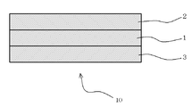
- FIG. 1 is a cross-sectional view of an anisotropic conductive film which is a preferred embodiment of the electrical connection material of the present invention.
- the conductive particle-containing layer 1 has a first insulating thermosetting resin composition layer 2 and a second insulating thermosetting resin composition. It has a structure sandwiched between layers 3.
- the conductive particle-containing layer 1 is formed by light irradiation of a conductive particle-containing resin composition layer containing an acrylate radical polymerizable compound, a photo radical polymerization initiator, an epoxy non-radical polymerizable compound, and conductive particles. B-staged by radical polymerization.
- “B stage” means a state in which the curable resin composition is semi-cured and flows or softens by heating.
- the conductive particle-containing resin composition layer which is a precursor of the conductive particle-containing layer 1 before photoradical polymerization, is composed of an acrylate radical polymerizable compound, a photo radical polymerization initiator, an epoxy non-radical polymerizable compound, and conductive particles. However, it does not contain a polymerization initiator for polymerizing the epoxy non-radically polymerizable compound. This is because epoxy non-radicals are formed by polymerization of the first insulating thermosetting resin composition layer 2 and the second insulating thermosetting resin composition layer 3 laminated on both surfaces of the conductive particle-containing layer 1. This is because the polymerizable compound is polymerized.
- the reaction rate of the acrylate radical polymerizable compound in the photo radical polymerization generated by light irradiation is preferably 70% or more. If the reaction rate is 70% or more, the effect of suppressing the flow of particles at the time of connection can be sufficiently obtained.
- the reaction rate can be measured by a known method such as FT-IR. The case where the reaction rate is 100% is also within the scope of the present invention.
- the conductive particle-containing layer 1 contains an unpolymerized epoxy-based non-radically polymerizable compound, the conductive particle-containing layer 1 As a whole, it can be said that it is not a fully cured state but a B stage state.
- the light irradiation conditions (light source, light wavelength, light intensity, light amount, temperature, etc.) can be set as appropriate.
- Examples of the acrylate-based radical polymerizable compound include monofunctional or polyfunctional (meth) acrylate (where (meth) acrylate is a term including acrylate and methacrylate).
- Monofunctional (meth) acrylate compounds include methyl (meth) acrylate, ethyl (meth) acrylate, n or i-propyl (meth) acrylate, n, i, sec or tert-butyl (meth) acrylate, 2-ethylhexyl ( And (meth) acrylate, benzyl (meth) acrylate, and dicyclopentanyl acrylate compounds.
- Polyfunctional (meth) acrylate compounds include ethylene glycol di (meth) acrylate, diethylene glycol di (meth) acrylate, 1,6-hexanediol di (meth) acrylate, propylene glycol di (meth) acrylate, dipropylene glycol di ( Bifunctional (meth) acrylate compounds such as (meth) acrylate, 1,2-cyclohexanediol di (meth) acrylate, neopentyl glycol di (meth) acrylate, dicyclopentadiene dimethacrylate, glycerin tri (meth) acrylate, trimethylol Examples of trifunctional (meth) acrylate compounds such as propane tri (meth) acrylate, pentaerythritol tri (meth) acrylate, tris (2-acryloyloxyethyl) isocyanurate It can be.
- epoxy-modified, urethane-modified, ethylene oxide-modified, and propylene oxide-modified products can also be used.
- bisphenol A type epoxy acrylate can be preferably used from the viewpoint of connection stability after curing.
- the photo radical polymerization initiator can be appropriately selected from known photo radical polymerization initiators. Examples include acetophenone photopolymerization initiators, benzyl ketal photopolymerization initiators, ⁇ -alkylaminophenone photopolymerization initiators, and phosphorus photopolymerization initiators. Specifically, 2-hydroxy-2-cyclohexylacetophenone (IRGACURE 184, BASF Japan Ltd.), ⁇ -hydroxy- ⁇ , ⁇ ′-dimethylacetophenone (Darocur) as an acetophenone photopolymerization initiator.
- acetophenone photopolymerization initiators include acetophenone photopolymerization initiators, benzyl ketal photopolymerization initiators, ⁇ -alkylaminophenone photopolymerization initiators, and phosphorus photopolymerization initiators.
- 2-hydroxy-2-cyclohexylacetophenone IRGACURE 184, BASF Japan Ltd.
- benzyl ketal photopolymerization initiators examples include benzophenone, fluorenone, dibenzosuberone, 4-aminobenzophenone, 4,4'-diaminobenzophenone, 4-hydroxybenzophenone, 4-chlorobenzophenone, 4,4'-dichlorobenzophenone, etc. It is done. Further, 2-benzyl-2-dimethylamino-1- (4-morpholinophenyl) -butanone-1 (IRGACURE 369, BASF Japan Ltd.) was used as an ⁇ -alkylaminophenone photopolymerization initiator. Can be used.
- phosphorous photopolymerization initiators bis (2,4,6-trimethylbenzoyl) -phenylphosphine oxide (IRGACURE 819, BASF Japan Ltd.), (2,4,6-trimethylbenzoyl) -diphenyl Phosphine oxide (DAROCURE TPO, BASF Japan Ltd.) etc. are mentioned.
- the compounding amount of the photo radical polymerization initiator is preferably 0.1 to 40 parts by mass, more preferably 0.5 to 30 parts by mass with respect to 100 parts by mass of the acrylate radical polymerizable compound. If it is this range, radical photopolymerization can fully advance and the fall of the mechanical strength of the electroconductive particle content layer 1 can be suppressed.
- a combination of the acrylate radical polymerizable compound and the photo radical polymerization initiator a combination of a bisphenol A type epoxy acrylate and an ⁇ -alkylaminophenone photo polymerization initiator can be exemplified.
- the epoxy-based non-radical polymerizable compound may be liquid or solid, and the epoxy equivalent is usually about 100 to 4000, and there is no radical polymerizable unsaturated bond in the molecule, and two or more epoxy groups are present.
- the compound which has can be mentioned.
- a bisphenol A type epoxy compound, a phenol novolac type epoxy compound, a cresol novolac type epoxy compound, an ester type epoxy compound, an alicyclic epoxy compound, or the like can be preferably used. These compounds include monomers and oligomers.
- the compounding amount of the epoxy non-radically polymerizable compound is preferably 3 to 250 parts by mass, more preferably 10 to 150 parts by mass with respect to 100 parts by mass of the acrylate radical polymerizable compound. If it is this range, an adhesive force can be improved and the change of an excessive curvature can be suppressed.
- the conductive particle-containing layer 1 includes a phenoxy resin, an epoxy resin, an unsaturated polyester resin, a saturated polyester resin, and a urethane as a film forming resin.
- Resins, butadiene resins, polyimide resins, polyamide resins, polyolefin resins, and the like can be included.
- the blending amount of such a film-forming resin component is preferably 10 to 200 parts by mass, more preferably 20 to 150 parts per 100 parts by mass in total of the acrylate radical polymerizable compound and the epoxy non-radical polymerizable compound. Part by mass. If it is this range, the handleability before hardening can be improved and the residual stress after hardening which also becomes a factor of curvature can be suppressed.
- conductive particles constituting a known anisotropic conductive film can be employed.
- examples thereof include metal particles such as nickel, and metal-coated resin particles in which a metal plating film such as nickel is formed on the surface of the resin core.
- An insulating thin film may be formed as necessary.
- the average particle size of such conductive particles is preferably 1 to 20 ⁇ m, more preferably 2 to 10 ⁇ m, from the viewpoint of electrical conductivity retention.
- the blending amount of the conductive particles is preferably 2 to 200 parts by mass with respect to a total of 100 parts by mass of the acrylate radical polymerizable compound, the epoxy non-radical polymerizable compound, and the film-forming resin blended as necessary. More preferred is 5 to 150 parts by mass. If it is this range, conduction
- Conductive particle density in the conductive particle-containing layer 1, from the viewpoint of securing the short-circuit prevention of conduction preferably from 1000 to 150,000 / mm 2, more preferably from 2000 to 100,000 / mm 2.
- the conductive particles in the conductive particle-containing layer 1 may be present in a form in which the conductive particles are uniformly mixed in the conductive particle-containing resin composition and formed into a single layer using a known technique such as a transfer mold. It is good also as a form arranged regularly by.
- the layer thickness of the conductive particle-containing layer 1 is preferably 1 to 20 ⁇ m, more preferably 2 to 10 ⁇ m, and even more preferably 3 to 8 ⁇ m. If it is this range, particle
- Each of these resin composition layers independently contains an epoxy non-radical polymerizable compound and a thermal cationic polymerization initiator or a thermal anionic polymerization initiator.
- the epoxy-based non-radical polymerizable compound may be liquid or solid, and the epoxy equivalent is usually about 100 to 4000, and there is no radical polymerizable unsaturated bond in the molecule, and two or more epoxy groups are present.
- the compound which has can be mentioned.
- a bisphenol A type epoxy compound, a phenol novolac type epoxy compound, a cresol novolac type epoxy compound, an ester type epoxy compound, an alicyclic epoxy compound, or the like can be preferably used. These compounds include monomers and oligomers.
- a particularly preferred epoxy-based non-radically polymerizable compound is a bisphenol A type epoxy compound from the viewpoint of connection stability after curing.
- thermal cationic polymerization initiator a known thermal cationic polymerization initiator for initiating cationic polymerization of an epoxy compound can be used.
- known iodonium salts, sulfonium salts, phosphonium salts, ferrocenes, etc. can be used.
- Aromatic sulfonium salts that can be used and exhibit good potential with respect to temperature can be preferably used.
- thermal cationic polymerization initiator examples include diphenyliodonium hexafluoroantimonate, diphenyliodonium hexafluorophosphate, diphenyliodonium hexafluoroborate, triphenylsulfonium hexafluoroantimonate, triphenylsulfonium hexafluorophosphate, triphenyls.
- Rufonium hexafluoroborate is exemplified.
- the amount of the thermal cationic polymerization initiator is preferably 0.1 to 40 parts by mass, more preferably 0.5 to 30 parts by mass with respect to parts.
- thermal anion polymerization initiator a known thermal anion polymerization initiator for initiating anionic polymerization of an epoxy compound can be used.
- an aliphatic amine compound, an aromatic amine compound, a secondary or tertiary amine Compounds, imidazole compounds, polymercaptan compounds, boron trifluoride-amine complexes, dicyandiamide, organic acid hydrazides, etc., preferably encapsulated imidazole compounds showing good potential with respect to temperature can do.
- Specific examples include NovaCure HX3941HP manufactured by Asahi Kasei E-Materials Corporation.
- the amount of the thermal anionic polymerization initiator is preferably 0.1 to 200 parts by mass, more preferably 0.5 to 150 parts by mass with respect to parts.
- the difference in cure shrinkage between the first insulating thermosetting resin composition layer 2 and the second insulating thermosetting resin composition layer 3 was created using the anisotropic conductive film of the present invention. In order to further suppress the warpage of the connection body, it is preferably 10% or less.
- the cure shrinkage rate can be measured according to JISK6901.
- the cure shrinkage of each layer is preferably within 10%, more preferably within 5%, and even more preferably within 3%.
- the layer thicknesses of the first insulating thermosetting resin composition layer 2 and the second insulating thermosetting resin composition layer 3 are each preferably 0.1 to 30 ⁇ m, more preferably 1 to 20 ⁇ m. If it is this range, particle
- the electrical connection material of the present invention has been described by taking an anisotropic conductive film as an example.
- the electrical connection material of the present invention includes an anisotropic conductive film, anisotropic conductive paste, conductive paste, conductive film, etc. Can take the form.
- the electrical connection material such as the anisotropic conductive film of the present invention can be produced by a production method having Step 1 and Step 2 described below.
- a conductive particle-containing resin composition containing an acrylate radical polymerizable compound, a photo radical polymerization initiator, an epoxy non-radical polymerizable compound, and conductive particles is formed, and light is applied to the resulting film.
- a conductive particle-containing layer by photoradical polymerization and B-stage.
- the conductive particle-containing resin composition is composed of an acrylate radical polymerizable compound, a photo radical polymerization initiator, an epoxy non-radical polymerizable compound, conductive particles, and other film forming components blended as necessary. It can prepare by mixing with a component uniformly by well-known methods, for example, a planetary mixer etc. The film formation can also be performed by a known means such as a doctor blade method. In this case, the conductive particle-containing resin composition layer in an uncured state is formed by forming a conductive particle-containing resin composition on a release-treated base sheet (for example, a peel-treated polyester sheet) and drying it as necessary. Can be formed.
- a release-treated base sheet for example, a peel-treated polyester sheet
- the conductive particle-containing resin composition layer thus formed is irradiated with light such as ultraviolet rays to photoradically polymerize the acrylate radical polymerizable compound.
- the reaction rate of the acrylate radical polymerizable compound is 70. % Or more, preferably 90% or more.
- a B-staged conductive particle-containing layer is formed.
- a second insulating thermosetting resin composition layer containing an epoxy non-radical polymerizable compound and a thermal cationic polymerization initiator or a thermal anionic polymerization initiator is laminated on the surface. Thereby, electrical connection materials, such as the anisotropic conductive film of this invention, are obtained.
- the first insulating thermosetting resin composition layer and the second insulating thermosetting resin composition layer can be prepared as follows. First of all, together with other components such as an epoxy non-radically polymerizable compound and a thermal cationic polymerization initiator or a thermal anionic polymerization initiator and a film-forming component blended as necessary, it is uniform by a known method such as a planetary mixer. Insulating thermosetting resin compositions are respectively prepared by mixing them. A first insulating thermosetting resin composition in an uncured state by depositing this resin composition on a release-treated base sheet by a known means such as a doctor blade method and drying it as necessary. A layer and a second insulating thermosetting resin composition layer are prepared.
- the first insulating thermosetting resin composition layer is overlaid on the previously formed conductive particle-containing layer and pressed.
- the anisotropic conductive film of the present invention is peeled off by peeling off the peeling base sheet on the conductive particle-containing layer side, overlaying the second insulating thermosetting resin composition layer, and pressing the resulting laminate.
- An electrical connection material such as is obtained.
- the conductive particle-containing layer peeled off from the release treatment base sheet was sandwiched between the first insulating thermosetting resin composition layer and the second insulating thermosetting resin composition layer, and the resulting laminate was obtained.
- An electrical connection material such as the anisotropic conductive film of the present invention can also be obtained by pressure bonding an object.
- the electrical connection material such as the anisotropic conductive film of the present invention includes terminals (for example, bumps) of the first electrical component (for example, IC chip) and terminals (for example, bumps) of the second electrical component (for example, wiring board). Between the first and second electrical components and by electrical connection, preferably anisotropic conductive connection, from the first or second electrical component side.
- Examples 1-7, Comparative Examples 1-4 Formation of first insulating thermosetting resin composition layer
- a first insulating thermosetting resin composition mixed solution of 50% solid content is prepared using toluene, and this mixed solution is applied onto a release PET base sheet. It apply
- Second insulating thermosetting resin composition layer (Formation of second insulating thermosetting resin composition layer) According to the composition shown in Table 1 (unit: parts by mass), a second insulating resin composition mixed solution of 50% solid content is prepared using toluene, and this mixed solution is dried on a peeled PET base sheet. It apply
- Thermocompression bonding conditions 180 ° C., 80 MPa, 5 seconds IC chip size: 1.5 mm ⁇ 20 mm, 0.5 mmt IC chip bump: gold-plated bump, 30 ⁇ m ⁇ 85 ⁇ m, bump height 15 ⁇ m, bump pitch 50 ⁇ m Size of glass substrate provided with 200 nm thick ITO pattern electrode: 50 mm ⁇ 30 mm, 0.3 mmt (1737F, Corning)
- connection body was measured for “initial conduction resistance”, “conduction resistance after high temperature and high humidity load test (conduction reliability)”, and “warping of the connection body”. The obtained results are shown in Table 1.
- Initial conduction resistance The initial conduction resistance of the connection body immediately after preparation was measured using a commercially available resistance measuring instrument. Practically, it is desired to be 10 ⁇ or less.
- connection warping Regarding the warpage of the connection body, the surface of the glass substrate on which the IC chip is not mounted was measured using a commercially available three-dimensional shape measurement system (Keyence Co., Ltd.) with a width of 20 mm corresponding to the back side of the IC chip. . It is desirable that the warpage is within 10 ⁇ m.
- the anisotropic conductive films of Examples 1 to 7 had excellent conduction reliability and little warpage.
- the anisotropic conductive film of Example 4 whose rigidity is comparatively low because the blending amount of acrylate is comparatively small, and the anisotropic conductive film of Example 6 whose comparatively low rigidity is low because the reaction rate is comparatively low
- the relatively low rigidity of the anisotropic conductive film is less likely to warp.
- the anisotropic conductive films of Examples 5 and 7 having relatively high rigidity are easily warped.
- Comparative Examples 1, 2, and 4 light irradiation was not performed on the conductive particle-containing layer, and thus there was a problem in conduction reliability.
- Comparative Example 3 although light irradiation was performed on the conductive particle-containing layer, there was a problem in conduction reliability because no photoradical polymerization initiator was contained. Further, since it contained a thermal radical polymerization initiator, it was immediately cured at the time of anisotropic conductive connection and warped greatly.
- the electrical connection material such as the anisotropic conductive film of the present invention
- the conduction reliability of the connected body is not lowered. Therefore, the anisotropic conductive film of the present invention is useful when flip-chip mounting an electrical component such as an IC chip on another electrical component such as a wiring board.
Landscapes
- Chemical & Material Sciences (AREA)
- Organic Chemistry (AREA)
- Engineering & Computer Science (AREA)
- Health & Medical Sciences (AREA)
- Chemical Kinetics & Catalysis (AREA)
- Medicinal Chemistry (AREA)
- Polymers & Plastics (AREA)
- Spectroscopy & Molecular Physics (AREA)
- Physics & Mathematics (AREA)
- Microelectronics & Electronic Packaging (AREA)
- Dispersion Chemistry (AREA)
- Manufacturing & Machinery (AREA)
- Non-Insulated Conductors (AREA)
- Adhesives Or Adhesive Processes (AREA)
- Adhesive Tapes (AREA)
- Polymerisation Methods In General (AREA)
- Electric Connection Of Electric Components To Printed Circuits (AREA)
- Wire Bonding (AREA)
- Organic Insulating Materials (AREA)
Abstract
Description
導電粒子含有層が、アクリレート系ラジカル重合性化合物と、光ラジカル重合開始剤と、エポキシ系非ラジカル重合性化合物と、導電粒子とを含有する導電粒子含有樹脂組成物層を光照射により光ラジカル重合させてBステージ化したものであり、
第1の絶縁性熱硬化型樹脂組成物層及び第2の絶縁性熱硬化型樹脂組成物層が、それぞれエポキシ系非ラジカル重合性化合物と熱カチオン重合開始剤又は熱アニオン重合開始剤とを含有していることを特徴とする電気接続材料を提供する。
アクリレート系ラジカル重合性化合物と、光ラジカル重合開始剤と、エポキシ系非ラジカル重合性化合物と、導電粒子とを含有する導電粒子含有樹脂組成物を成膜し、得られた膜に対し光を照射して光ラジカル重合させBステージ化することにより導電粒子含有層を形成する工程、及び
導電粒子含有層の片面に、エポキシ系非ラジカル重合性化合物と熱カチオン重合開始剤又は熱アニオン重合開始剤とを含有している第1の絶縁性熱硬化型樹脂組成物層、他面にエポキシ系非ラジカル重合性化合物と熱カチオン重合開始剤又は熱アニオン重合開始剤とを含有している第2の絶縁性熱硬化型樹脂組成物層を積層する工程
を有する製造方法を提供する。
図1に示すように、本発明の異方性導電フィルム10は、導電粒子含有層1が、第1の絶縁性熱硬化型樹脂組成物層2と第2の絶縁性熱硬化型樹脂組成物層3とで挟持された構造を有する。
この導電粒子含有層1は、アクリレート系ラジカル重合性化合物と、光ラジカル重合開始剤と、エポキシ系非ラジカル重合性化合物と、導電粒子とを含有する導電粒子含有樹脂組成物層を光照射により光ラジカル重合させてBステージ化したものである。ここで、“Bステージ”とは硬化型樹脂組成物が半硬化した状態であって、加熱により流動もしくは軟化する状態を意味する。
これらの樹脂組成物層は、それぞれ独立的に、エポキシ系非ラジカル重合性化合物と熱カチオン重合開始剤又は熱アニオン重合開始剤とを含有する。
本発明の異方性導電フィルム等の電気接続材料は、以下に説明する工程1と工程2とを有する製造方法により製造することができる。
まず、アクリレート系ラジカル重合性化合物と、光ラジカル重合開始剤と、エポキシ系非ラジカル重合性化合物と、導電粒子とを含有する導電粒子含有樹脂組成物を成膜し、得られた膜に対し光を照射して光ラジカル重合させBステージ化することにより導電粒子含有層を形成する。
次に、導電粒子含有層の片面に、エポキシ系非ラジカル重合性化合物と熱カチオン重合開始剤又は熱アニオン重合開始剤とを含有している第1の絶縁性熱硬化型樹脂組成物層、他面にエポキシ系非ラジカル重合性化合物と熱カチオン重合開始剤又は熱アニオン重合開始剤とを含有している第2の絶縁性熱硬化型樹脂組成物層を積層する。これにより、本発明の異方性導電フィルム等の電気接続材料が得られる。
本発明の異方性導電フィルム等の電気接続材料は、第1の電気部品(例えば、ICチップ)の端子(例えばバンプ)と、第2の電気部品(例えば配線基板)の端子(例えばバンプ、パッド)との間に配置し、第1又は第2の電気部品側から熱圧着により電気接続、好ましくは異方性導電接続することにより接続体を与えることができる。
(第1の絶縁性熱硬化型樹脂組成物層の形成)
表1に示す配合(単位:質量部)に従って、トルエンを用いて50%固形分の第1の絶縁性熱硬化型樹脂組成物混合液を調製し、この混合液を剥離PETベースシート上に、乾燥厚が8μmとなるように塗布し、80℃で5分間乾燥することにより、第1の絶縁性熱硬化型樹脂組成物層を形成した。
表1に示す配合(単位:質量部)に従って、トルエンを用いて50%固形分の第2の絶縁性樹脂組成物混合液を調製し、この混合液を剥離PETベースシート上に、乾燥厚が8μmとなるように塗布し、80℃で5分間乾燥することにより、第2の絶縁性熱硬化型樹脂組成物層を形成した。
表1に示す配合(単位:質量部)に従って、トルエンを用いて50%固形分の導電粒子含有樹脂組成物混合液を調製し、この混合液を剥離PETベースシート上に、乾燥厚が6μmとなるように塗布し、80℃で5分間乾燥し、続いて、紫外線を表1の積算光量となるように照射して光ラジカル重合させることにより導電粒子含有層を形成した。この導電粒子含有層におけるアクリレート系ラジカル重合性化合物の反応率を、FT-IR(FT/IR-4100、日本分光(株))を用いて測定し、得られた結果を表1に示した。
第1の絶縁性熱硬化型樹脂組成物層に導電粒子含有層を重ね合わせ、ラミネートした後、導電粒子含有層側の剥離PETベースシートを剥がし、導電粒子含有層を露出させた。その露出した導電粒子含有層に第2の絶縁性熱硬化型樹脂組成物層を重ね合わせ、剥離PETベースシート上から、40℃、0.1Paの条件でラミネートすることにより、異方性導電フィルムを得た。
(接続体の作成)
各実施例及び比較例で作成した異方性導電フィルムを用いて、ICチップのバンプとガラス基板のITOパターン電極との間を、熱圧着により異方性導電接続した。なお、異方性接続時には第一の絶縁性樹脂組成物層をICチップ側に配置した。
ICチップのサイズ:1.5mm×20mm、0.5mmt
ICチップのバンプ:金メッキバンプ、30μm×85μm、バンプ高さ15μm、バンプピッチ50μm
200nm厚のITOパターン電極が設けられたガラス基板のサイズ:50mm×30mm、0.3mmt(1737F、コーニング社)
得られた接続体について、以下に説明するように、「初期導通抵抗」、「高温高湿負荷試験後の導通抵抗(導通信頼性)」、「接続体の反り」について測定した。得られた結果を表1に示す。
作成直後の接続体の初期導通抵抗を市販の抵抗測定器を用いて測定した。実用上、10Ω以下であることが望まれる。
接続体を、85℃、85%Rhに維持されたチャンバー中で1000時間放置した後の接続体の導通抵抗を市販の抵抗測定器を用いて測定した。実用上、15Ω以下であることが望まれる。
接続体の反りについては、ICチップが実装されていない側のガラス基板表面を、ICチップの裏側に相当する巾20mmを、市販の三次元形状測定システム((株)キーエンス)を用いて測定した。反りが10μm以内であることが望まれる。

実施例1~7の異方性導電フィルムは、導通信頼性に優れ、反りも少ないものであった。なお、アクリレートの配合量が比較的少ないために剛性が比較的低い実施例4の異方性導電フィルムと、反応率が比較的低いために剛性が比較的低い実施例6の異方性導電フィルムとの結果から、異方性導電フィルムの剛性が比較的低い方が反り難いことが分かる。また逆に、剛性が比較的高い実施例5や実施例7の異方性導電フィルムの場合、反り易くなっていることがわかる。
2 第1の絶縁性熱硬化型樹脂組成物層
3 第2の絶縁性熱硬化型樹脂組成物層
Claims (8)
- 導電粒子含有層が、第1の絶縁性熱硬化型樹脂組成物層と第2の絶縁性熱硬化型樹脂組成物層とで挟持された電気接続材料であって、
導電粒子含有層が、アクリレート系ラジカル重合性化合物と、光ラジカル重合開始剤と、エポキシ系非ラジカル重合性化合物と、導電粒子とを含有する導電粒子含有樹脂組成物層を光照射により光ラジカル重合させてBステージ化したものであり、
第1の絶縁性熱硬化型樹脂組成物層及び第2の絶縁性熱硬化型樹脂組成物層が、それぞれエポキシ系非ラジカル重合性化合物と熱カチオン重合開始剤又は熱アニオン重合開始剤とを含有していることを特徴とする電気接続材料。 - 導電粒子含有層中において、アクリレート系ラジカル重合性化合物の反応率が70%以上である請求項1記載の電気接続材料。
- アクリレート系ラジカル重合性化合物が、ビスフェノールA型エポキシアクリレートであり、光ラジカル重合開始剤が、α-アルキルアミノフェノン系光重合開始剤である請求項1又は2記載の電気接続材料。
- エポキシ系非ラジカル重合性化合物が、ビスフェノールA型エポキシ化合物であり、熱カチオン重合開始剤が、芳香族スルホニウム塩である請求項1~3のいずれかに記載の電気接続材料。
- 第1の絶縁性熱硬化型樹脂組成物層と第2の絶縁性熱硬化型樹脂組成物層との間の硬化収縮率差が10%以下である請求項1~4のいずれかに記載の電気接続材料。
- 請求項1記載の電気接続材料の製造方法であって、
アクリレート系ラジカル重合性化合物と、光ラジカル重合開始剤と、エポキシ系非ラジカル重合性化合物と、導電粒子とを含有する導電粒子含有樹脂組成物を成膜し、得られた膜に対し光を照射して光ラジカル重合させBステージ化することにより導電粒子含有層を形成する工程、及び
導電粒子含有層の片面に、エポキシ系非ラジカル重合性化合物と熱カチオン重合開始剤又は熱アニオン重合開始剤とを含有している第1の絶縁性熱硬化型樹脂組成物層、他面にエポキシ系非ラジカル重合性化合物と熱カチオン重合開始剤又は熱アニオン重合開始剤とを含有している第2の絶縁性熱硬化型樹脂組成物層を積層する工程
を有する製造方法。 - 導電粒子含有樹脂組成物の膜に対し、アクリレート系ラジカル重合性化合物の反応率が70%以上となるように光を照射する請求項6記載の製造方法。
- 第1の電気部品の端子と第2の電気部品の端子とを、請求項1~5のいずれかに記載の電気接続材料を介して熱圧着により電気接続してなる接続体。
Priority Applications (3)
| Application Number | Priority Date | Filing Date | Title |
|---|---|---|---|
| US15/027,422 US10154587B2 (en) | 2013-10-15 | 2014-09-17 | Electrical connection material |
| KR1020167008851A KR101828192B1 (ko) | 2013-10-15 | 2014-09-17 | 전기 접속 재료 |
| CN201480054982.0A CN105594064B (zh) | 2013-10-15 | 2014-09-17 | 电连接材料、其制备方法及连接体 |
Applications Claiming Priority (2)
| Application Number | Priority Date | Filing Date | Title |
|---|---|---|---|
| JP2013215095A JP6187126B2 (ja) | 2013-10-15 | 2013-10-15 | 電気接続材料 |
| JP2013-215095 | 2013-10-15 |
Publications (1)
| Publication Number | Publication Date |
|---|---|
| WO2015056512A1 true WO2015056512A1 (ja) | 2015-04-23 |
Family
ID=52827965
Family Applications (1)
| Application Number | Title | Priority Date | Filing Date |
|---|---|---|---|
| PCT/JP2014/074510 Ceased WO2015056512A1 (ja) | 2013-10-15 | 2014-09-17 | 電気接続材料 |
Country Status (6)
| Country | Link |
|---|---|
| US (1) | US10154587B2 (ja) |
| JP (1) | JP6187126B2 (ja) |
| KR (1) | KR101828192B1 (ja) |
| CN (1) | CN105594064B (ja) |
| TW (1) | TWI627639B (ja) |
| WO (1) | WO2015056512A1 (ja) |
Families Citing this family (4)
| Publication number | Priority date | Publication date | Assignee | Title |
|---|---|---|---|---|
| JP6750197B2 (ja) * | 2015-07-13 | 2020-09-02 | デクセリアルズ株式会社 | 異方性導電フィルム及び接続構造体 |
| CN114787307B (zh) * | 2019-12-03 | 2024-11-22 | 迪睿合株式会社 | 各向异性导电膜 |
| KR20230056827A (ko) * | 2021-10-20 | 2023-04-28 | 에이치엔에스하이텍 (주) | 도전입자의 유동성을 제어한 이방도전성 접착필름의 제조방법 |
| KR20230056826A (ko) * | 2021-10-20 | 2023-04-28 | 에이치엔에스하이텍 (주) | 도전입자의 유동성을 제어한 이방도전성 접착필름 |
Citations (12)
| Publication number | Priority date | Publication date | Assignee | Title |
|---|---|---|---|---|
| JPH08148212A (ja) * | 1994-11-25 | 1996-06-07 | Hitachi Chem Co Ltd | 接続部材及び該接続部材を用いた電極の接続構造・接続法 |
| JPH08148210A (ja) * | 1994-11-25 | 1996-06-07 | Hitachi Chem Co Ltd | 接続部材 |
| JPH08148213A (ja) * | 1994-11-25 | 1996-06-07 | Hitachi Chem Co Ltd | 接続部材、該接続部材を用いた電極の接続構造及び接続方法 |
| JPH11273771A (ja) * | 1998-03-26 | 1999-10-08 | Hitachi Chem Co Ltd | 接続部材 |
| JP2003342338A (ja) * | 2002-03-18 | 2003-12-03 | Dainippon Printing Co Ltd | 樹脂組成物および光学素子 |
| WO2007083810A1 (ja) * | 2006-01-23 | 2007-07-26 | Hitachi Chemical Co., Ltd. | 接着剤組成物、フィルム状接着剤、接着シート、並びにそれを用いた半導体装置 |
| JP2009242771A (ja) * | 2008-03-11 | 2009-10-22 | Hitachi Chem Co Ltd | 感光性接着剤組成物、接着シート、接着剤パターン、接着剤層付半導体ウェハ、並びに半導体装置及びその製造方法 |
| JP2011070931A (ja) * | 2009-09-25 | 2011-04-07 | Sekisui Chem Co Ltd | 異方性導電材料、接続構造体の製造方法及び接続構造体 |
| JP2013058413A (ja) * | 2011-09-08 | 2013-03-28 | Sekisui Chem Co Ltd | 絶縁材料、積層体、接続構造体、積層体の製造方法及び接続構造体の製造方法 |
| JP2013057017A (ja) * | 2011-09-08 | 2013-03-28 | Sekisui Chem Co Ltd | 絶縁材料、積層体、接続構造体、積層体の製造方法及び接続構造体の製造方法 |
| JP2013140756A (ja) * | 2012-01-06 | 2013-07-18 | Sekisui Chem Co Ltd | 絶縁材料、多層フィルム、積層体、接続構造体、積層体の製造方法及び接続構造体の製造方法 |
| JP2013143291A (ja) * | 2012-01-11 | 2013-07-22 | Sekisui Chem Co Ltd | 絶縁材料、多層フィルム、積層体、接続構造体、積層体の製造方法及び接続構造体の製造方法 |
Family Cites Families (5)
| Publication number | Priority date | Publication date | Assignee | Title |
|---|---|---|---|---|
| EP1489117B1 (en) | 2002-03-18 | 2007-05-09 | Dai Nippon Printing Co., Ltd. | Resin composition and optical element |
| KR100601341B1 (ko) * | 2004-06-23 | 2006-07-14 | 엘에스전선 주식회사 | 이방 도전성 접착제 및 이를 이용한 접착필름 |
| JP4534716B2 (ja) | 2004-10-26 | 2010-09-01 | 日立化成工業株式会社 | 回路接続材料並びに回路端子の接続構造体及び接続方法 |
| JP5754378B2 (ja) * | 2010-01-22 | 2015-07-29 | コニカミノルタ株式会社 | インクジェットヘッドの製造方法 |
| WO2012137838A1 (ja) * | 2011-04-08 | 2012-10-11 | 太陽インキ製造株式会社 | 感光性組成物、その硬化皮膜及びそれらを用いたプリント配線板 |
-
2013
- 2013-10-15 JP JP2013215095A patent/JP6187126B2/ja active Active
-
2014
- 2014-09-17 KR KR1020167008851A patent/KR101828192B1/ko active Active
- 2014-09-17 WO PCT/JP2014/074510 patent/WO2015056512A1/ja not_active Ceased
- 2014-09-17 CN CN201480054982.0A patent/CN105594064B/zh active Active
- 2014-09-17 US US15/027,422 patent/US10154587B2/en active Active
- 2014-10-09 TW TW103135171A patent/TWI627639B/zh active
Patent Citations (12)
| Publication number | Priority date | Publication date | Assignee | Title |
|---|---|---|---|---|
| JPH08148212A (ja) * | 1994-11-25 | 1996-06-07 | Hitachi Chem Co Ltd | 接続部材及び該接続部材を用いた電極の接続構造・接続法 |
| JPH08148210A (ja) * | 1994-11-25 | 1996-06-07 | Hitachi Chem Co Ltd | 接続部材 |
| JPH08148213A (ja) * | 1994-11-25 | 1996-06-07 | Hitachi Chem Co Ltd | 接続部材、該接続部材を用いた電極の接続構造及び接続方法 |
| JPH11273771A (ja) * | 1998-03-26 | 1999-10-08 | Hitachi Chem Co Ltd | 接続部材 |
| JP2003342338A (ja) * | 2002-03-18 | 2003-12-03 | Dainippon Printing Co Ltd | 樹脂組成物および光学素子 |
| WO2007083810A1 (ja) * | 2006-01-23 | 2007-07-26 | Hitachi Chemical Co., Ltd. | 接着剤組成物、フィルム状接着剤、接着シート、並びにそれを用いた半導体装置 |
| JP2009242771A (ja) * | 2008-03-11 | 2009-10-22 | Hitachi Chem Co Ltd | 感光性接着剤組成物、接着シート、接着剤パターン、接着剤層付半導体ウェハ、並びに半導体装置及びその製造方法 |
| JP2011070931A (ja) * | 2009-09-25 | 2011-04-07 | Sekisui Chem Co Ltd | 異方性導電材料、接続構造体の製造方法及び接続構造体 |
| JP2013058413A (ja) * | 2011-09-08 | 2013-03-28 | Sekisui Chem Co Ltd | 絶縁材料、積層体、接続構造体、積層体の製造方法及び接続構造体の製造方法 |
| JP2013057017A (ja) * | 2011-09-08 | 2013-03-28 | Sekisui Chem Co Ltd | 絶縁材料、積層体、接続構造体、積層体の製造方法及び接続構造体の製造方法 |
| JP2013140756A (ja) * | 2012-01-06 | 2013-07-18 | Sekisui Chem Co Ltd | 絶縁材料、多層フィルム、積層体、接続構造体、積層体の製造方法及び接続構造体の製造方法 |
| JP2013143291A (ja) * | 2012-01-11 | 2013-07-22 | Sekisui Chem Co Ltd | 絶縁材料、多層フィルム、積層体、接続構造体、積層体の製造方法及び接続構造体の製造方法 |
Also Published As
| Publication number | Publication date |
|---|---|
| TW201530563A (zh) | 2015-08-01 |
| JP6187126B2 (ja) | 2017-08-30 |
| KR101828192B1 (ko) | 2018-02-09 |
| CN105594064B (zh) | 2019-03-05 |
| KR20160052674A (ko) | 2016-05-12 |
| TWI627639B (zh) | 2018-06-21 |
| JP2015079603A (ja) | 2015-04-23 |
| US20160255724A1 (en) | 2016-09-01 |
| CN105594064A (zh) | 2016-05-18 |
| US10154587B2 (en) | 2018-12-11 |
Similar Documents
| Publication | Publication Date | Title |
|---|---|---|
| JP6372543B2 (ja) | 異方性導電フィルム及びその製造方法 | |
| JP7170612B2 (ja) | 異方性導電フィルムの製造方法及び異方性導電フィルム | |
| WO2014021457A1 (ja) | 異方性導電フィルム及びその製造方法 | |
| JP6187126B2 (ja) | 電気接続材料 | |
| CN105940564A (zh) | 各向异性导电膜及其制造方法 | |
| JP2016103634A (ja) | 光硬化系異方性導電接着剤、接続体の製造方法及び電子部品の接続方法 | |
| CN106715622B (zh) | 自由基聚合型粘接剂组合物以及电连接体的制造方法 | |
| CN103502379A (zh) | 各向异性导电连接材料、膜层叠体、连接方法及连接结构体 | |
| WO2015119090A1 (ja) | 異方性導電フィルム及びその製造方法 | |
| JP2014202821A (ja) | 液晶表示素子の製造方法及び接合材料 | |
| JP6232855B2 (ja) | ラジカル重合型接着剤組成物、及び電気接続体の製造方法 | |
| CN103748167B (zh) | 热阳离子聚合性组合物、各向异性导电粘接膜、连接结构体及其制造方法 | |
| TWI651195B (zh) | 異向性導電膜及其製造方法 | |
| HK1224826A1 (en) | Electrical connection material, method for producing the same and connected body | |
| WO2015119098A1 (ja) | 異方性導電フィルム及びその製造方法 | |
| HK1224826B (zh) | 电连接材料、其制备方法及连接体 |
Legal Events
| Date | Code | Title | Description |
|---|---|---|---|
| 121 | Ep: the epo has been informed by wipo that ep was designated in this application |
Ref document number: 14853605 Country of ref document: EP Kind code of ref document: A1 |
|
| DPE2 | Request for preliminary examination filed before expiration of 19th month from priority date (pct application filed from 20040101) | ||
| ENP | Entry into the national phase |
Ref document number: 20167008851 Country of ref document: KR Kind code of ref document: A |
|
| WWE | Wipo information: entry into national phase |
Ref document number: 15027422 Country of ref document: US |
|
| NENP | Non-entry into the national phase |
Ref country code: DE |
|
| 122 | Ep: pct application non-entry in european phase |
Ref document number: 14853605 Country of ref document: EP Kind code of ref document: A1 |