WO2015037348A1 - 炭化珪素半導体装置 - Google Patents
炭化珪素半導体装置 Download PDFInfo
- Publication number
- WO2015037348A1 WO2015037348A1 PCT/JP2014/069797 JP2014069797W WO2015037348A1 WO 2015037348 A1 WO2015037348 A1 WO 2015037348A1 JP 2014069797 W JP2014069797 W JP 2014069797W WO 2015037348 A1 WO2015037348 A1 WO 2015037348A1
- Authority
- WO
- WIPO (PCT)
- Prior art keywords
- electrode
- silicon carbide
- gate
- semiconductor device
- schottky
- Prior art date
- Legal status (The legal status is an assumption and is not a legal conclusion. Google has not performed a legal analysis and makes no representation as to the accuracy of the status listed.)
- Ceased
Links
Images




Classifications
-
- H—ELECTRICITY
- H10—SEMICONDUCTOR DEVICES; ELECTRIC SOLID-STATE DEVICES NOT OTHERWISE PROVIDED FOR
- H10D—INORGANIC ELECTRIC SEMICONDUCTOR DEVICES
- H10D84/00—Integrated devices formed in or on semiconductor substrates that comprise only semiconducting layers, e.g. on Si wafers or on GaAs-on-Si wafers
- H10D84/101—Integrated devices comprising main components and built-in components, e.g. IGBT having built-in freewheel diode
- H10D84/141—VDMOS having built-in components
- H10D84/146—VDMOS having built-in components the built-in components being Schottky barrier diodes
-
- H—ELECTRICITY
- H10—SEMICONDUCTOR DEVICES; ELECTRIC SOLID-STATE DEVICES NOT OTHERWISE PROVIDED FOR
- H10D—INORGANIC ELECTRIC SEMICONDUCTOR DEVICES
- H10D30/00—Field-effect transistors [FET]
- H10D30/60—Insulated-gate field-effect transistors [IGFET]
- H10D30/64—Double-diffused metal-oxide semiconductor [DMOS] FETs
- H10D30/66—Vertical DMOS [VDMOS] FETs
- H10D30/668—Vertical DMOS [VDMOS] FETs having trench gate electrodes, e.g. UMOS transistors
-
- H—ELECTRICITY
- H10—SEMICONDUCTOR DEVICES; ELECTRIC SOLID-STATE DEVICES NOT OTHERWISE PROVIDED FOR
- H10D—INORGANIC ELECTRIC SEMICONDUCTOR DEVICES
- H10D62/00—Semiconductor bodies, or regions thereof, of devices having potential barriers
- H10D62/80—Semiconductor bodies, or regions thereof, of devices having potential barriers characterised by the materials
- H10D62/83—Semiconductor bodies, or regions thereof, of devices having potential barriers characterised by the materials being Group IV materials, e.g. B-doped Si or undoped Ge
- H10D62/832—Semiconductor bodies, or regions thereof, of devices having potential barriers characterised by the materials being Group IV materials, e.g. B-doped Si or undoped Ge being Group IV materials comprising two or more elements, e.g. SiGe
- H10D62/8325—Silicon carbide
-
- H—ELECTRICITY
- H10—SEMICONDUCTOR DEVICES; ELECTRIC SOLID-STATE DEVICES NOT OTHERWISE PROVIDED FOR
- H10D—INORGANIC ELECTRIC SEMICONDUCTOR DEVICES
- H10D64/00—Electrodes of devices having potential barriers
- H10D64/01—Manufacture or treatment
- H10D64/012—Manufacture or treatment of electrodes comprising a Schottky barrier to a semiconductor
- H10D64/0121—Manufacture or treatment of electrodes comprising a Schottky barrier to a semiconductor to Group IV semiconductors
- H10D64/0123—Manufacture or treatment of electrodes comprising a Schottky barrier to a semiconductor to Group IV semiconductors to silicon carbide
-
- H—ELECTRICITY
- H10—SEMICONDUCTOR DEVICES; ELECTRIC SOLID-STATE DEVICES NOT OTHERWISE PROVIDED FOR
- H10D—INORGANIC ELECTRIC SEMICONDUCTOR DEVICES
- H10D64/00—Electrodes of devices having potential barriers
- H10D64/60—Electrodes characterised by their materials
- H10D64/64—Electrodes comprising a Schottky barrier to a semiconductor
-
- H—ELECTRICITY
- H10—SEMICONDUCTOR DEVICES; ELECTRIC SOLID-STATE DEVICES NOT OTHERWISE PROVIDED FOR
- H10D—INORGANIC ELECTRIC SEMICONDUCTOR DEVICES
- H10D84/00—Integrated devices formed in or on semiconductor substrates that comprise only semiconducting layers, e.g. on Si wafers or on GaAs-on-Si wafers
- H10D84/80—Integrated devices formed in or on semiconductor substrates that comprise only semiconducting layers, e.g. on Si wafers or on GaAs-on-Si wafers characterised by the integration of at least one component covered by groups H10D12/00 or H10D30/00, e.g. integration of IGFETs
- H10D84/811—Combinations of field-effect devices and one or more diodes, capacitors or resistors
-
- H—ELECTRICITY
- H10—SEMICONDUCTOR DEVICES; ELECTRIC SOLID-STATE DEVICES NOT OTHERWISE PROVIDED FOR
- H10D—INORGANIC ELECTRIC SEMICONDUCTOR DEVICES
- H10D12/00—Bipolar devices controlled by the field effect, e.g. insulated-gate bipolar transistors [IGBT]
- H10D12/01—Manufacture or treatment
- H10D12/031—Manufacture or treatment of IGBTs
-
- H—ELECTRICITY
- H10—SEMICONDUCTOR DEVICES; ELECTRIC SOLID-STATE DEVICES NOT OTHERWISE PROVIDED FOR
- H10D—INORGANIC ELECTRIC SEMICONDUCTOR DEVICES
- H10D62/00—Semiconductor bodies, or regions thereof, of devices having potential barriers
- H10D62/40—Crystalline structures
- H10D62/405—Orientations of crystalline planes
-
- H—ELECTRICITY
- H10—SEMICONDUCTOR DEVICES; ELECTRIC SOLID-STATE DEVICES NOT OTHERWISE PROVIDED FOR
- H10D—INORGANIC ELECTRIC SEMICONDUCTOR DEVICES
- H10D8/00—Diodes
- H10D8/01—Manufacture or treatment
- H10D8/051—Manufacture or treatment of Schottky diodes
-
- H—ELECTRICITY
- H10—SEMICONDUCTOR DEVICES; ELECTRIC SOLID-STATE DEVICES NOT OTHERWISE PROVIDED FOR
- H10D—INORGANIC ELECTRIC SEMICONDUCTOR DEVICES
- H10D8/00—Diodes
- H10D8/60—Schottky-barrier diodes
Definitions
- the present invention relates to a silicon carbide semiconductor device. More specifically, the present invention relates to a silicon carbide semiconductor device including a transistor element and a Schottky barrier diode.
- SiC silicon carbide
- SBD Schottky barrier diode
- a silicon carbide semiconductor device has a DMOSFET region and an SBD region.
- the SBD region is a region different from the DMOSFET region.
- the SBD is composed of a portion of the drain region of the field effect transistor that is not covered with the gate insulating film and a metal.
- the SBD is formed between two cells of a MOSFET.
- Japanese Unexamined Patent Application Publication No. 2009-194127 does not specifically disclose the arrangement of SBD regions in a semiconductor device.
- a semiconductor device is realized in the form of a semiconductor chip.
- the SBD region and the DMOSFET region By arranging both the SBD region and the DMOSFET region in the semiconductor device, there arises a problem that the area of the semiconductor chip increases.
- the SBD is integrated with the transistor cell. This increases the size of the transistor cell.
- an SBD is disposed between a plurality of transistor cells. For this reason, the space
- An object of the present invention is to provide a silicon carbide semiconductor device capable of integrating transistor elements and Schottky barrier diodes while avoiding a decrease in active region.
- a silicon carbide semiconductor device includes a silicon carbide layer having a first main surface and a second main surface located on the opposite side to the first main surface.
- the silicon carbide layer has a first conductivity type, a drift layer that defines the first main surface of the silicon carbide layer, and a second conductivity type that is provided in the drift layer and is different from the first conductivity type.
- a body region provided with at least one opening exposing the drift layer.
- a silicon carbide semiconductor device includes: a gate insulating film disposed on a first main surface of a silicon carbide layer and having a first contact hole for exposing the first main surface at a position corresponding to the opening;
- the Schottky electrode that is Schottky-bonded to the drift layer, the gate electrode that is disposed on the gate insulating film, and the gate insulating film, the gate electrode, and the Schottky electrode are covered through the first contact hole and the opening.
- a gate pad electrode electrically connected to the electrode.
- the present invention it is possible to provide a silicon carbide semiconductor device capable of integrating transistor elements and Schottky barrier diodes while avoiding a decrease in active region.
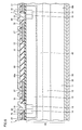
- FIG. 1 is a plan view schematically showing a configuration of silicon carbide semiconductor device 1 according to a first embodiment of the present invention.
- FIG. 2 is a cross-sectional view taken along line II-II in FIG. It is a top view which shows arrangement
- 1 is an equivalent circuit diagram of a silicon carbide semiconductor device 1 according to a first embodiment. It is a circuit diagram showing an example of an inverter circuit configured by silicon carbide semiconductor device 1 according to the first embodiment. It is a top view which shows roughly the structure of 1 A of silicon carbide semiconductor devices which concern on the 2nd Embodiment of this invention.
- FIG. 1 is a plan view schematically showing a configuration of silicon carbide semiconductor device 1 according to a first embodiment of the present invention.
- FIG. 2 is a cross-sectional view taken along line II-II in FIG. It is a top view which shows
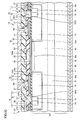
- FIG. 8 is a partial cross-sectional view of silicon carbide semiconductor device 1A taken along line VIII-VIII in FIG.
- FIG. 5 is a cross-sectional view schematically showing a state in which a reverse bias voltage is applied between the drain electrode and the source pad electrode in the configuration shown in FIG. 4. It is sectional drawing which showed typically the state in which the reverse bias voltage was applied to 1 A of silicon carbide semiconductor devices which concern on 2nd Embodiment.
- FIG. 7 is a plan view schematically showing a configuration of a silicon carbide semiconductor device 1B according to a third embodiment of the present invention.
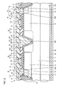
- FIG. 12 is a partial cross-sectional view taken along line XII-XII in FIG.
- FIG. 6 is a plan view showing another embodiment of the arrangement of the Schottky electrode 25.
- FIG. 6 is a plan view showing still another embodiment of the arrangement of the Schottky electrode 25.
- a silicon carbide semiconductor device (1, 1A, 1B) includes a first main surface (10a) and a first main surface (10a) positioned opposite to the first main surface (10a).
- a silicon carbide layer (10) having two main surfaces (10b) is provided.
- the silicon carbide layer (10) has a first conductivity type, and is provided on the drift layer (12) defining the first main surface (10a) of the silicon carbide layer (10) and the drift layer (12).
- a body region (13) having a second conductivity type different from the first conductivity type and provided with at least one opening (30a) exposing the drift layer (12).
- Silicon carbide semiconductor devices (1, 1A, 1B) are arranged on first main surface (10a) of silicon carbide layer (10), and first main surface (10a) is formed on opening (30a).
- a Schottky junction is formed on the drift layer (12) through the gate insulating film (15) in which the first contact hole (GH1) to be exposed is formed, the first contact hole (GH1), and the opening (30a).
- the Schottky electrode (25), the gate electrode (27) disposed on the gate insulating film (15), the gate insulating film (15), the gate electrode (27), and the Schottky electrode (25) are covered.
- the insulating layer (70) so as to overlap the Schottky electrode (25) in a plan view with the insulating layer (70) disposed and having the second contact hole for exposing the gate electrode (27) formed In It is location, and a gate electrode (27) electrically connected to the gates pad electrode (59) through the second contact hole.
- the gate pad electrode occupies a relatively large area in the semiconductor chip.
- a Schottky barrier diode is formed under the gate pad electrode. No transistor element is formed below the gate pad electrode. For this reason, reduction of the active region can be prevented.
- plan view corresponds to viewing the first main surface (or the second main surface) along the normal direction of the first main surface.
- the opening (30a) is disposed inside the first contact hole (GH1).
- the Schottky electrode (25) is Schottky joined to both the drift layer (12) and the body region (13).
- the Schottky electrode is also Schottky joined to the first region, the Schottky electrode can directly inject and withdraw carriers from the first region. Therefore, the breakdown voltage can be ensured more reliably.
- the depletion layer can be reduced more quickly by injecting carriers from the Schottky electrode into the body region.
- the reduction of the depletion layer is also referred to as “cancellation of depletion”.
- the depletion layer when a reverse bias voltage is applied between the drift layer and the body region, the depletion layer can be expanded more quickly by extracting carriers from the Schottky electrode. Thereby, a withstand voltage can be ensured.
- the silicon carbide layer (10) is disposed in the body region (13), the first region (14) having the first conductivity type, and the body region (13), And a second region (18) having a second conductivity type.
- the insulating layer (70) is disposed so as to cover the gate insulating film (15) and the gate electrode (27), the third contact hole for exposing the Schottky electrode (25), the first and second The first interlayer insulating film (71) in which the fourth contact holes for exposing the regions (14, 18) are formed, and the second interlayer insulating film (71) disposed on the first interlayer insulating film (71). Interlayer insulating film (72).
- the silicon carbide semiconductor device (1, 1A, 1B) is disposed on the first interlayer insulating film (71), and is electrically connected to the Schottky electrode (25) through the third contact hole. And a source pad electrode electrically connected to the first and second regions (14, 18) through the four contact holes.
- the transistor and the free wheel diode can be integrated in one semiconductor chip.
- a circuit including a transistor and a free wheel diode, such as an inverter circuit can be realized with a smaller and simpler configuration.
- At least one opening (30a) is a plurality of openings separated from each other by a distance.
- the gate electrode (27) is electrically connected to the gate pad electrode (59) at the outer periphery of the gate pad electrode (59).
- the plurality of openings are arranged on the inner side of the gate electrode (27) and are arranged so as to surround the central portion (40, 45) of the gate pad electrode (59).
- the plurality of openings are arranged at intervals from each other, thereby preventing a region inside the plurality of openings and a region outside the plurality of openings from being divided. be able to. Therefore, the potential of one of these two regions (for example, a region outside the plurality of openings) can be prevented from becoming a floating potential.
- the possibility of damage to the Schottky barrier diode can be reduced.
- the probe needle may come into contact with the gate pad electrode.
- a wire is connected to the gate pad electrode.
- an impact is likely to be applied to the central portion of the gate pad electrode.
- the length of the interval between the plurality of openings (30a) is constant. According to this structure, it can prevent that the area
- the opening (30a) has a groove (TR) that passes through the body region (13) and reaches the drift layer (12).
- the Schottky electrode (25) is disposed so as to cover the inner peripheral surface of the groove (TR).
- the area of the Schottky electrode to be Schottky joined to the silicon carbide layer can be increased. Therefore, more carriers can be injected and extracted through the Schottky electrode.
- the first conductivity type is n-type
- the second conductivity type is p-type. According to this configuration, the ease of manufacturing the silicon carbide semiconductor device can be improved.
- FIG. 1 is a plan view schematically showing a configuration of silicon carbide semiconductor device 1 according to the first embodiment of the present invention.
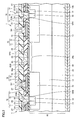
- FIG. 2 is a sectional view taken along line II-II in FIG. 1 and 2
- silicon carbide semiconductor device 1 according to one embodiment of the present invention includes a silicon carbide layer 10, a gate insulating film 15, a source electrode 16, a gate electrode 27, and a Schottky electrode. 25, an insulating layer 70, a gate pad electrode 59, a gate runner 66, a source pad electrode 65, a drain electrode 20, and a back surface protective electrode 50.
- Silicon carbide layer 10 has a first main surface 10a and a second main surface 10b.
- the second main surface 10b is located on the opposite side to the first main surface 10a.
- Silicon carbide layer 10 has an n + substrate 11 and a drift layer 12.
- N + substrate 11 is made of, for example, polytype 4H hexagonal silicon carbide.
- the n + substrate 11 contains a high concentration of impurities (donor).
- the concentration of impurities contained in n + substrate 11 is, for example, about 1.0 ⁇ 10 18 cm ⁇ 3 .
- the type of impurity is, for example, N (nitrogen).
- the drift layer 12 is disposed on the n + substrate 11.
- Drift layer 12 is a layer formed by, for example, epitaxial growth.
- Drift layer 12 is made of, for example, polytype 4H hexagonal silicon carbide.
- the surface of drift layer 12 defines first main surface 10a of silicon carbide layer 10.
- the impurity concentration in the drift layer 12 is lower than the impurity concentration in the n + substrate 11.
- the impurity concentration contained in the drift layer 12 is about 7.5 ⁇ 10 15 cm ⁇ 3 .
- the thickness of the drift layer 12 is, for example, about 10 ⁇ m or more and about 35 ⁇ m or less.
- the impurity contained in the drift layer 12 is, for example, nitrogen.
- silicon carbide semiconductor device 1 includes a plurality of transistor elements 7.
- the transistor element 7 is a MOSFET (Metal Oxide Semiconductor Field Effect Transistor).
- a body region 13 is arranged in the drift layer 12 to constitute a MOSFET.
- source region 14 (first region) and p + region 18 (second region) are arranged in body region 13.
- the body region 13 is a region having a p-type different from the n-type.
- the impurity concentration in the deep part of the body region is about 1 ⁇ 10 18 cm ⁇ 3 .
- the thickness of body region 13 is not less than about 0.5 ⁇ m and not more than about 1.0 ⁇ m, for example.
- an opening 30a is provided in a part of the body region 13 located below the gate pad electrode 59. Opening 30a exposes drift layer 12 to first main surface 10a of the silicon carbide layer. That is, the conductivity type of the region below the opening 30a is n-type.
- the source region 14 is a region having n type.
- the concentration of impurities contained in the source region 14 is higher than the concentration of impurities contained in the drift layer 12.
- Source region 14 contains, for example, an impurity such as P (phosphorus) at a concentration of about 1 ⁇ 10 20 cm ⁇ 3 .
- the p + region 18 is a region having a p-type.
- the p + region 18 is disposed in contact with the source region 14.
- the concentration of impurities contained in p + region 18 is higher than the concentration of impurities contained in body region 13.
- the p + region 18 contains impurities such as aluminum and boron at a concentration of about 1 ⁇ 10 20 cm ⁇ 3 , for example.
- the gate insulating film 15 is provided at a position facing the channel region CH formed in the body region 13. Gate insulating film 15 is in contact with body region 13, source region 14, and drift layer 12 at first main surface 10 a of silicon carbide layer 10. Gate insulating film 15 is made of, for example, silicon dioxide. The thickness of the gate insulating film 15 (the dimension of the gate insulating film 15 along the normal direction of the first main surface 10a) is, for example, about 50 nm.
- a contact hole GH 1 (first contact hole) is formed at a position overlapping the opening 30 a, and a contact hole GH 2 is formed at a position overlapping the source region 14 and the p + region 18.
- Contact holes GH1 and GH2 expose first main surface 10a of silicon carbide layer 10. More specifically, the contact hole GH1 exposes the drift layer 12 through the opening 30a. Contact hole GH2 exposes source region 14 and p + region 18.
- the Schottky electrode 25 is disposed under the gate pad electrode 59.
- Schottky electrode 25 is Schottky joined to drift layer 12 through contact hole GH1 and opening 30a.
- the Schottky electrode 25 and the silicon carbide layer 10 form a Schottky barrier diode (SBD) under the gate pad electrode 59.
- SBD Schottky barrier diode
- the material of Schottky electrode 25 is not particularly limited as long as it is a metal that can achieve a Schottky junction with drift layer 12, that is, the silicon carbide semiconductor layer.
- a metal that can achieve a Schottky junction with drift layer 12 that is, the silicon carbide semiconductor layer.
- the gate electrode 27 is disposed on the gate insulating film 15. Gate electrode 27 faces drift layer 12, source region 14, and body region 13 so as to extend from the source region 14 of transistor element 7 to the other source region 14.
- the gate electrode 27 is made of a conductor such as polysilicon doped with impurities or aluminum.
- the insulating layer 70 is disposed so as to cover the gate insulating film 15, the gate electrode 27, and the Schottky electrode 25.
- a contact hole SH (second contact hole) for exposing the gate electrode 27 is formed in the insulating layer 70.
- the insulating layer 70 includes a first interlayer insulating film 71 and a second interlayer insulating film 72.
- the first interlayer insulating film 71 is disposed so as to cover the gate insulating film 15 and the gate electrode 27.
- the first interlayer insulating film 71 is made of silicon dioxide.
- the thickness of first interlayer insulating film 71 is, for example, about 1 ⁇ m.
- the second interlayer insulating film 72 is disposed on the first interlayer insulating film 71.
- the second interlayer insulating film 72 is made of silicon dioxide.
- the thickness of second interlayer insulating film 72 is, for example, about 1 ⁇ m.
- the second interlayer insulating film 72 may be a film having higher strength than the first interlayer insulating film 71.
- the second interlayer insulating film 72 may be a film made of silicon nitride (SiN).
- the contact hole SH is a contact hole that penetrates the first interlayer insulating film 71 and the second interlayer insulating film 72.
- a contact hole SHa third contact hole for exposing the Schottky electrode 25, and the source region 14 and the p + region 18 are exposed.
- Contact hole SHb fourth contact hole is formed.
- the contact holes SHb and GH2 are contact holes that penetrate the first interlayer insulating film 71 and the gate insulating film 15.
- Source electrode 16 is arranged in contact holes SHb and GH2 and contacts source region 14 and p + region 18. Thereby, source electrode 16 is electrically connected to source region 14 and p + region 18.
- the source electrode 16 is made of a material having nickel and silicon.
- the source electrode 16 may be made of a material having titanium, aluminum, and silicon.
- source electrode 16 is in ohmic contact with source region 14 and p + region 18.
- the source pad electrode 65 is disposed on the first interlayer insulating film 71.
- Source pad electrode 65 is made of, for example, aluminum.
- the source pad electrode 65 is electrically connected to the Schottky electrode 25 through the contact hole SHa. Further, the source pad electrode 65 is electrically connected to the source electrode 16 through the contact holes SHb and GH2.
- the gate pad electrode 59 and the gate runner 66 are disposed on the second interlayer insulating film 72.
- Gate pad electrode 59 and gate runner 66 are made of aluminum, for example. However, the gate runner 66 is not shown in FIG.
- the gate pad electrode 59 is disposed on the second interlayer insulating film 72 so as to cover the Schottky electrode 25. As shown in FIG. 1, the gate pad electrode 59 overlaps the Schottky electrode 25 in plan view.
- the gate pad electrode 59 is electrically connected to the gate electrode 27 through a contact hole SH formed in the insulating layer 70 (the first interlayer insulating film 71 and the second interlayer insulating film 72).
- Drain electrode 20 is in contact with second main surface 10b of silicon carbide layer 10. Thereby, the drain electrode 20 is electrically connected to the n + substrate 11.
- the drain electrode 20 may have a configuration similar to that of the source electrode 16, for example.
- the drain electrode 20 may be made of another material capable of ohmic contact with the n + substrate 11 such as nickel.
- the back surface protective electrode 50 is disposed in contact with the drain electrode 20.
- the back surface protective electrode 50 is made of, for example, titanium, nickel, silver, or an alloy thereof.
- the drain electrode 20 is the drain electrode of the MOSFET and the cathode of the SBD.
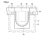
- FIG. 3 is a plan view showing the arrangement of the gate pad electrode, the gate electrode, and the Schottky electrode.
- gate electrode 27 overlaps with gate pad electrode 59 at the outer periphery of gate pad electrode 59 in plan view. In other words, the gate electrode 27 is not formed in a region corresponding to the central portion of the gate pad electrode 59.
- the gate electrode 27 is electrically connected to the gate pad electrode 59 at the outer periphery of the gate pad electrode 59. As described above, the gate pad electrode 59 is electrically connected to the gate electrode 27 through the contact hole SH formed in the insulating layer 70 (not shown in FIG. 3).
- the gate runner 66 is connected to the gate pad electrode 59 and to the gate electrode 27 through the contact hole SH.
- a capacitor is formed by the gate electrode 27, the gate insulating film 15 (see FIG. 2), and the body region 13. As the area of the gate electrode 27 increases, the capacitance value of the capacitor increases. As the capacitance value increases, the delay time of the signal transmitted through the gate electrode 27 increases. In order to avoid such a problem, the gate electrode 27 is formed below the gate pad electrode 59 so as to have an area as small as possible while ensuring electrical connection with the gate pad electrode 59.
- the gate electrode 27 is formed so as to overlap the outer peripheral portion of the gate pad electrode 59 immediately below the gate pad electrode 59. Further, the gate runner 66 is disposed so as to surround the gate electrode 27 and is electrically connected to the gate electrode 27.
- the Schottky electrode 25 is disposed inside the gate electrode 27.
- the Schottky electrode 25 is arranged so as to be surrounded by the body region 13. That is, there is no discontinuous portion in the body region 13. Therefore, it is possible to prevent the body region 13 from generating a portion where the potential is floating.
- FIG. 4 is a diagram showing a general structure below the gate pad electrode. Referring to FIG. 4, body region 13 is present below gate pad electrode 59 through first interlayer insulating film 71 and gate insulating film 15.
- the gate pad electrode 59 occupies a relatively large area in the semiconductor chip. However, no MOSFET is formed in the region immediately below the gate pad electrode 59.
- the probe needle when testing a silicon carbide semiconductor device, the probe needle may come into contact with the gate pad electrode. In the wire bonding step, a wire is connected to the gate pad electrode. In these cases, a relatively large force is applied to the gate pad electrode 59. When an element is manufactured in a region under the gate pad electrode 59, there is a concern that the element is damaged by an impact applied to the gate pad electrode. Therefore, in the structure shown in FIG. 4, an element such as a MOSFET is not formed below the gate pad electrode 59.
- the Schottky electrode 25 is formed below the gate pad electrode 59.
- an SBD is formed below the gate pad electrode 59.
- the region below the gate pad electrode 59 is a region where no transistor element is formed. By forming the SBD in this region, it is possible to prevent a decrease in the active region. Since the SBD is composed of the Schottky electrode 25 and the silicon carbide layer 10, the structure is simple. Therefore, the SBD can be disposed below the gate pad electrode 59.
- the element when an element is manufactured in the region under the gate pad electrode 59, there is a concern that the element may be damaged by an impact applied to the gate pad electrode.
- two interlayer insulating films 71 and 72 are stacked between the gate pad electrode 59 and the Schottky electrode 25. Therefore, the SBD formed below the gate pad electrode 59 can be protected from an impact applied to the gate pad electrode 59.
- FIG. 5 is an equivalent circuit diagram of silicon carbide semiconductor device 1 according to the first embodiment.
- silicon carbide semiconductor device 1 includes a MOS transistor M1 and a Schottky barrier diode D1.
- the MOS transistor M1 represents an integrated transistor element 7.
- the drain electrode of the MOS transistor M1 and the cathode electrode of the Schottky barrier diode D1 are electrically connected.
- the drain electrode of the MOS transistor M1 and the cathode electrode of the Schottky barrier diode D1 are realized by the drain electrode 20.
- the source electrode of the MOS transistor M1 and the anode electrode of the Schottky barrier diode D1 are electrically connected.
- the source electrode of the MOS transistor M1 is realized by the source electrode 16 (and the source pad electrode 65) shown in FIG.
- the anode electrode of the Schottky barrier diode D1 is realized by the Schottky electrode 25.
- the Schottky electrode 25 is electrically connected to the source of the MOSFET through the source electrode 16 and the source pad electrode 65.
- FIG. 6 is a circuit diagram showing an example of an inverter circuit configured by silicon carbide semiconductor device 1 according to the first embodiment.
- inverter circuit 101 is, for example, a single-phase inverter.
- the inverter circuit 101 is connected to the positive electrode and the negative electrode of the DC power supply 8 via the positive electrode terminal 5 and the negative electrode terminal 6, respectively.
- the inverter circuit 101 converts DC power supplied from the DC power supply 8 into single-phase AC.
- Single phase load 9A is an inductive load, for example, a single phase motor.
- the type of the single-phase load 9A is not particularly limited.
- Inverter circuit 101 includes silicon carbide semiconductor devices 1-1 to 1-4.
- the configuration of each of silicon carbide semiconductor devices 1-1 to 1-4 is the same as the configuration shown in FIG. Therefore, each of silicon carbide semiconductor devices 1-1 to 1-4 can be realized by silicon carbide semiconductor device 1 according to the present embodiment.
- Silicon carbide semiconductor devices 1-1 and 1-2 are connected in series between positive electrode terminal 5 and negative electrode terminal 6.
- silicon carbide semiconductor devices 1-3 and 1-4 are connected in series between positive electrode terminal 5 and negative electrode terminal 6.
- the inverter circuit 101 may be a three-phase inverter.
- two silicon carbide semiconductor devices connected in series between positive electrode terminal 5 and negative electrode terminal 6 may be added to the configuration shown in FIG.
- a large current such as a surge current can be generated. This surge current may damage the MOS transistor.
- a freewheeling diode is connected in antiparallel to the MOS transistor.
- the freewheeling diode is realized by a chip different from the MOS transistor or a discrete element.
- the MOS transistor and the SBD are integrated on one semiconductor chip. Therefore, the inverter circuit can be realized with a smaller and simpler configuration. Therefore, it is possible to construct a system that is superior in cost.
- the SBD When the SBD is disposed inside a region where the transistor elements 7 are integrated (referred to as an element region), the number of transistor elements disposed in the element region is reduced. That is, the area of the active region of the silicon carbide semiconductor device is reduced.
- the SBD is formed in the region below the gate pad electrode 59. While the region below the gate pad electrode 59 has a relatively large area, no transistor element is formed. Therefore, the formation of the SBD in this region can avoid a decrease in the active region.
- the plurality of openings 30a are formed in the body region 13, and the Schottky electrode 25 is Schottky-joined to the drift layer 12 in each of the plurality of openings 30a.
- an SBD having a sufficient size can be realized, so that a larger amount of current can flow through the SBD.
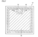
- FIG. 7 is a plan view schematically showing a configuration of silicon carbide semiconductor device 1A according to the second embodiment of the present invention.
- the configuration of silicon carbide semiconductor device 1 ⁇ / b> A is basically the same as that of silicon carbide semiconductor device 1 according to the first embodiment.
- Silicon carbide semiconductor device 1A according to the second embodiment is different from silicon carbide semiconductor device 1 according to the first embodiment in the arrangement of Schottky electrodes.
- this point will be described in detail.
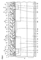
- FIG. 8 is a partial cross-sectional view of silicon carbide semiconductor device 1A taken along line VIII-VIII in FIG. 7 and 8, Schottky electrode 25 is arranged to cover both drift layer 12 and body region 13. In other words, the opening (30a) is disposed inside the first contact hole (GH1).
- the end portion 25 a of the Schottky electrode 25 covers the body region 13. Therefore, the Schottky electrode 25 is Schottky joined to both the body region 13 and the drift layer 12.
- the arrangement of the Schottky electrode 25 (in other words, the opening 30a) in the second embodiment is the same as the arrangement shown in FIG.
- the Schottky electrode 25 is joined not only to the drift layer 12 but also to the body region 13.
- This configuration can improve the switching characteristics of the silicon carbide semiconductor device 1A. Thereby, the breakdown voltage of silicon carbide semiconductor device 1A can be further increased. This effect will be described in more detail with reference to the drawings.
- FIG. 9 is a cross-sectional view schematically showing a state in which a reverse bias voltage is applied between the drain electrode and the source pad electrode in the configuration shown in FIG.
- the voltage between drain electrode 20 and source pad electrode 65 is set such that the potential of drain electrode 20 is higher than the potential of source pad electrode 65 when the MOSFET (transistor element 7) is off. Is applied.
- Such a state can occur during the operation of the inverter circuit 101 shown in FIG. In this case, the depletion layer 40 extends from the interface (junction) between the drift layer 12 and the body region 13.
- source pad electrode 65 cannot be arranged below gate pad electrode 59. Therefore, body region 13 is connected to source pad electrode 65 around gate pad electrode 59. Holes are injected into and extracted from body region 13 by p + region 18 and source pad electrode 65. However, the portion of the body region 13 below the gate pad electrode 59 is relatively far from the position where the source pad electrode 65 and the body region 13 are electrically connected (that is, the position of the p + region 18).
- the breakdown voltage of the transistor element 7 may be reduced.
- the reliability of the oxide film is likely to decrease as the impurity concentration in the p-type region increases.
- FIG. 10 is a cross-sectional view schematically showing a state in which a reverse bias voltage is applied to silicon carbide semiconductor device 1A according to the second embodiment.
- holes are injected from Schottky electrode 25.
- depletion of the portion of the body region 13 below the gate pad electrode 59 can be released in a short time without increasing the impurity concentration of the body region 13.
- the potential of the Schottky electrode 25 becomes lower than the potential of the drain electrode 20. In this case, electrons are extracted from the drift layer 12 by the drain electrode 20. On the other hand, holes are extracted from the body region 13 by the source pad electrode 65 and the Schottky electrode 25. With the Schottky electrode 25, the portion below the gate pad electrode 59 in the body region 13 can be depleted in a shorter time. By spreading the depletion layer 40 as soon as possible, the strength of the electric field applied to the depletion layer 40 can be lowered. Therefore, the breakdown voltage of silicon carbide semiconductor device 1A (MOSFET) can be improved.
- MOSFET silicon carbide semiconductor device 1A
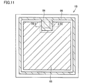
- FIG. 11 is a plan view schematically showing a configuration of silicon carbide semiconductor device 1B according to the third embodiment of the present invention.
- the configuration of silicon carbide semiconductor device 1 ⁇ / b> B is basically the same as that of silicon carbide semiconductor device 1 according to the first embodiment.
- Silicon carbide semiconductor device 1B according to the third embodiment is different from silicon carbide semiconductor device 1 according to the first embodiment in the cross-sectional shape of SBD.
- SBD cross-sectional shape of SBD
- FIG. 12 is a partial cross-sectional view taken along line XII-XII in FIG.
- opening 30a has a groove (trench TR).
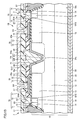
- Trench TR has side wall surface SW and bottom surface BT. That is, the opening 30a has a side wall surface SW and a bottom surface BT.
- Side wall surface SW is a surface inclined with respect to main surface 10a of silicon carbide layer 10 so as to approach main surface 10b of silicon carbide layer 10.
- the two opposing side wall surfaces SW expand in a tapered shape toward the first main surface 10a of the silicon carbide layer 10.
- Side wall surface SW is, for example, a surface inclined by 50 degrees or more and 80 degrees or less with respect to the ⁇ 000-1 ⁇ plane. More specifically, the side wall surface SW is macroscopically viewed in the plane orientations ⁇ 0-33-8 ⁇ , ⁇ 0-11-2 ⁇ , ⁇ 0-11-4 ⁇ and ⁇ 0-11-1 ⁇ . Any of the following. Note that “macroscopic” means ignoring a fine structure having a dimension on the order of atomic spacing. As such a macroscopic off-angle measurement, for example, a general method using X-ray diffraction can be used.
- Such an opening 30a can be formed by, for example, thermal etching.
- thermal etching is an etching process that is performed by exposing an object to be etched to an etching gas at a high temperature, and is a process that has substantially no physical etching action.
- the thermal etching process gas contains a halogen element. More preferably, the halogen element is chlorine or fluorine.
- a process gas containing at least one of Cl 2 , BCl 3, CF 4 , and SF 6 can be used as the process gas, and in particular, Cl 2 can be preferably used.
- the process gas preferably further contains oxygen gas.
- the process gas may contain a carrier gas.
- the carrier gas can be, for example, nitrogen gas, argon gas or helium gas.
- the heat treatment temperature of the thermal etching is preferably 700 ° C. or higher and 1200 ° C. or lower.
- the lower limit of this temperature is more preferably 800 ° C, and still more preferably 900 ° C.
- the etching rate can be set to a sufficiently practical value.
- the upper limit of this temperature is more preferably 1100 ° C., still more preferably 1000 ° C.
- the etching rate of SiC is, for example, about 70 ⁇ m / hour.
- Schottky electrode 25 is arranged so as to cover the inner peripheral surface (side wall surface SW and bottom surface BT) of trench TR. As shown in FIG. 15, the opening 30 a may be filled with the Schottky electrode 25.
- the third embodiment an effect similar to that of the first embodiment can be achieved.
- the area of the Schottky electrode 25 that is Schottky joined to the drift layer 12 can be increased. Therefore, more carriers can be injected and extracted through the Schottky electrode.
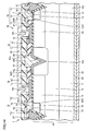
- FIG. 13 is a cross-sectional view showing another configuration of silicon carbide semiconductor device 1B according to the third embodiment.
- end 25a of Schottky electrode 25 covers body region 13.
- the Schottky electrode 25 is Schottky joined to the body region 13 at the end 25 a of the Schottky electrode 25.
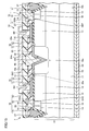
- FIG. 14 is a diagram showing still another configuration of the silicon carbide semiconductor device according to the third embodiment.
- bottom surface BT may be omitted from opening 30a. That is, the cross-sectional shape of the opening 30a may be V-shaped. According to such a configuration, the size of the opening 30a can be reduced.
- FIG. 15 is a diagram showing still another configuration of the silicon carbide semiconductor device according to the third embodiment.
- bottom surface BT is omitted from opening 30a.
- the end portion 25 a of the Schottky electrode 25 covers the body region 13.
- the size of the SBD can be reduced.
- the depletion layer 40 can be expanded more quickly. By expanding the depletion layer 40 earlier, the breakdown voltage can be further improved.
- a forward bias is applied to the SBD, depletion of the body region 13 and the drift region can be released earlier.
- the arrangement of the Schottky electrode 25 in plan view is not limited to the arrangement shown in FIG.
- FIG. 16 is a plan view showing another embodiment of the arrangement of the Schottky electrode 25.
- Schottky electrode 25 and opening 30a overlap each other.
- the plurality of Schottky electrodes 25 (in other words, the plurality of openings 30 a) are located inside the gate electrode 27 in a plan view and are disposed so as to surround the central portion 80 of the gate pad electrode 59.
- the central portion 80 is a region of the gate pad electrode 59 to which a wire (not shown) is connected.
- a strong force may be applied to the central portion 80 during wire bonding.
- a plurality of Schottky electrodes 25 are arranged so as to avoid the central portion 80 of the gate pad electrode 59. Thereby, the possibility that the SBD is damaged due to the impact on the gate pad electrode 59 can be further reduced.
- the plurality of Schottky electrodes 25 are separated at a constant interval a1.
- the drift layer 12 is exposed in the opening 30a.
- the region immediately below the opening 30a is an n-type region. For this reason, when one continuous (in other words, unbroken) opening is formed in the body region 13, the body region 13 is divided into a region inside the opening and a region outside the opening.
- the region outside the opening is given a potential by the source electrode 16 and the source pad electrode 65.
- the potential in the region inside the opening is a floating potential.
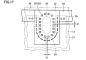
- FIG. 17 is a plan view showing still another embodiment of the arrangement of the Schottky electrode 25.
- the Schottky electrode 25 (opening 30a) shown in FIG. 17 is smaller than the Schottky electrode 25 (opening 30a) shown in FIG.
- the number of Schottky electrodes 25 (openings 30a) increases, and the gap portion also increases. Therefore, the potential difference between the region inside the plurality of openings 30a and the region outside the plurality of openings 30a can be further reduced.
- the plurality of Schottky electrodes 25 are not limited to one that surrounds the central portion 80 in a single layer.
- the plurality of Schottky electrodes 25 may double surround the central portion 80.
- the number of openings 30a may be singular. Also in this case, the opening 30a only needs to have a break in order to avoid the potential in the region inside the opening 30a from becoming a floating potential.
- the MOSFET is exemplified as the transistor disposed in the silicon carbide semiconductor device.
- the transistor element arranged in the silicon carbide semiconductor device according to this embodiment only needs to have a drift layer and a body region. Therefore, the transistor element may be, for example, an IGBT (Insulated Gate Bipolar Transistor).
- silicon carbide layer 10 includes n + substrate 11 and n-type drift layer 12.
- Silicon carbide layer 10 is an n-type silicon carbide layer as a whole. That is, in the above embodiment, the first conductivity type that is the conductivity type of silicon carbide layer 10 is n-type, and the second conductivity type that is the conductivity type of body region 13 is p-type. By forming the p-type region in the n-type silicon carbide layer, the ease of manufacturing the silicon carbide semiconductor device can be improved. However, the first conductivity type may be p-type and the second conductivity type may be n-type.
- 1, 1A, 1B Silicon carbide semiconductor device 5 positive terminal, 6 negative terminal, 7 transistor element, 8 DC power supply, 9A single phase load, 10 silicon carbide layer, 10a first main surface, 10b second main surface, 11 n + substrate, 12 drift layer, 13 body region, 14 source region, 15 gate insulating film, 16 source electrode, 18 p + region, 20 drain electrode, 25 Schottky electrode, 25a end (Schottky electrode), 27 Gate electrode, 30a opening, 40 depletion layer, 50 back surface protection electrode, 59 gate pad electrode, 65 source pad electrode, 66 gate runner, 70 insulating layer, 71 first interlayer insulating film, 72 second interlayer insulating film, 80 center portion (gate pad electrode), 101 inverter circuit, BT bottom surface, CH channel region, D1 Schottky barrier diode, GH1, GH , SH, SHa, SHb contact hole, M1 MOS transistor, SW side wall surface, TR trench, a1 interval.
Landscapes
- Electrodes Of Semiconductors (AREA)
- Drying Of Semiconductors (AREA)
Abstract
活性領域の減少を避けつつトランジスタ素子とショットキーバリアダイオードとを集積化することが可能な炭化珪素半導体装置を提供する。炭化珪素半導体装置(1)は、炭化珪素層(10)と、ゲート絶縁膜(15)と、第1のコンタクトホール(GH1)および開口部(30a)を通じて、ドリフト層(12)にショットキー接合されたショットキー電極(25)と、ゲート絶縁膜(15)上に配置されたゲート電極(27)と、ゲート絶縁膜(15)、ゲート電極(27)およびショットキー電極(25)を覆うように配置されて、ゲート電極(27)を露出させるための第2のコンタクトホールが形成された絶縁層(70)と、平面視においてショットキー電極(25)と重なるように、絶縁層(70)上に配置されて、第2のコンタクトホールを通じてゲート電極(27)と電気的に接続されたゲートパッド電極(59)とを備える。
Description
本発明は、炭化珪素半導体装置に関する。より特定的には、本発明は、トランジスタ素子とショットキーバリアダイオードとを備えた炭化珪素半導体装置に関する。
近年、半導体装置を構成する材料に炭化珪素(SiC)を採用することが進められつつある。炭化珪素基板を採用した半導体装置として、トランジスタ素子とショットキーバリアダイオード(以下、SBDとも呼ぶ)とを集積化した半導体装置が提案されている。
たとえば特開2009-194127号公報(特許文献1)によれば、炭化珪素半導体装置は、DMOSFET領域と、SBD領域とを有する。SBD領域は、DMOSFET領域とは異なる領域である。たとえば特開2003-229570号公報(特許文献2)によれば、SBDは、電界効果トランジスタのドレイン領域のうちのゲート絶縁膜に覆われていない部分と、金属とによって構成される。たとえば特開2009-88326号公報(特許文献3)によれば、SBDは、MOSFETの2つのセルの間に形成される。
特開2009-194127号公報は、半導体装置におけるSBD領域の配置を具体的に開示していない。一般に、半導体装置は半導体チップの形態で実現される。SBD領域とDMOSFET領域との両方を半導体装置に配置することにより、半導体チップの面積が増大するという問題が発生する。
一方、特開2003-229570号公報によれば、SBDがトランジスタセルに一体化される。このため、トランジスタセルのサイズが大きくなる。特開2003-229570号公報によれば、複数のトランジスタセルの間にSBDが配置される。このため、複数のトランジスタセル同士の間隔が大きくなる。これらの構成によれば、MOSFETの活性領域、すなわちMOSFETにおいて電流を流すことに寄与する領域の面積が減少する。言い換えると、ある大きさの電流を流すために必要な半導体チップの面積が増加する。
本発明の目的は、活性領域の減少を避けつつトランジスタ素子とショットキーバリアダイオードとを集積化することが可能な炭化珪素半導体装置を提供することである。
本発明の一局面に係る炭化珪素半導体装置は、第1の主面と、第1の主面に対して反対側に位置する第2の主面とを有する炭化珪素層を備える。炭化珪素層は、第1の導電型を有し、炭化珪素層の第1の主面を規定するドリフト層と、ドリフト層に設けられて、第1の導電型とは異なる第2の導電型を有し、ドリフト層を露出させる少なくとも1つの開口部が設けられたボディ領域とを含む。炭化珪素半導体装置は、炭化珪素層第1の主面上に配置されて、開口部に対応する位置に第1の主面を露出させるための第1のコンタクトホールが形成されたゲート絶縁膜と、第1のコンタクトホールおよび開口部を通じて、ドリフト層にショットキー接合されたショットキー電極と、ゲート絶縁膜上に配置されたゲート電極と、ゲート絶縁膜、ゲート電極およびショットキー電極を覆うように配置されて、ゲート電極を露出させるための第2のコンタクトホールが形成された絶縁層と、平面視においてショットキー電極と重なるように、絶縁層上に配置されて、第2のコンタクトホールを通じてゲート電極と電気的に接続されたゲートパッド電極とを備える。
本発明によれば、活性領域の減少を避けつつトランジスタ素子とショットキーバリアダイオードとを集積化することが可能な炭化珪素半導体装置を提供することができる。
[本願発明の実施形態の説明]
最初に本発明の実施形態を列記して説明する。
最初に本発明の実施形態を列記して説明する。
(1)本発明の実施形態に係る炭化珪素半導体装置(1,1A,1B)は、第1の主面(10a)と、第1の主面(10a)に対して反対側に位置する第2の主面(10b)とを有する炭化珪素層(10)を備える。炭化珪素層(10)は、第1の導電型を有し、炭化珪素層(10)の第1の主面(10a)を規定するドリフト層(12)と、ドリフト層(12)に設けられて、第1の導電型とは異なる第2の導電型を有し、ドリフト層(12)を露出させる少なくとも1つの開口部(30a)が設けられたボディ領域(13)とを含む。炭化珪素半導体装置(1,1A,1B)は、炭化珪素層(10)の第1の主面(10a)上に配置されて、開口部(30a)上に第1の主面(10a)を露出させるための第1のコンタクトホール(GH1)が形成されたゲート絶縁膜(15)と、第1のコンタクトホール(GH1)および開口部(30a)を通じて、ドリフト層(12)にショットキー接合されたショットキー電極(25)と、ゲート絶縁膜(15)上に配置されたゲート電極(27)と、ゲート絶縁膜(15)、ゲート電極(27)およびショットキー電極(25)を覆うように配置されて、ゲート電極(27)を露出させるための第2のコンタクトホールが形成された絶縁層(70)と、平面視においてショットキー電極(25)と重なるように、絶縁層(70)上に配置されて、第2のコンタクトホールを通じてゲート電極(27)と電気的に接続されたゲートパッド電極(59)とを備える。
この構成によれば、活性領域の減少を避けつつトランジスタ素子とショットキーバリアダイオードとを集積化することが可能な炭化珪素半導体装置を実現することができる。ゲートパッド電極は、半導体チップにおいて比較的大きな面積を占める。このゲートパッド電極の下方にショットキー電極を配置することにより、ゲートパッド電極の下にショットキーバリアダイオードが形成される。ゲートパッド電極の下方にはトランジスタ素子が形成されていない。このため、活性領域の減少を防ぐことができる。
なお、「平面視」とは、第1の主面の法線方向に沿って第1の主面(あるいは第2の主面)を見ることに相当する。
(2)好ましくは、開口部(30a)は、第1のコンタクトホール(GH1)の内側に配置される。ショットキー電極(25)は、ドリフト層(12)とボディ領域(13)との両方にショットキー接合される。
この構成によれば、ショットキー電極が第1の領域にもショットキー接合されているので、ショットキー電極が第1の領域に対して直接的にキャリアを注入および引き抜くことができる。したがって、より確実に耐圧を確保することができる。
ドリフト層とボディ領域との間に空乏層が存在する場合、ショットキー電極からボディ領域に対してキャリアを注入することで、空乏層をより速やかに縮小することができる。なお、この明細書では、空乏層の縮小を「空乏化の解除」とも呼ぶ。
一方、ドリフト層とボディ領域との間に逆バイアス電圧を印加する場合、ショットキー電極からキャリアを引き抜くことにより、空乏層をより速やかに広げることができる。これにより、耐圧を確保することができる。
(3)好ましくは、炭化珪素層(10)は、ボディ領域(13)に配置されて、第1の導電型を有する第1の領域(14)と、ボディ領域(13)に配置されて、第2の導電型を有する第2の領域(18)とをさらに含む。絶縁層(70)は、ゲート絶縁膜(15)およびゲート電極(27)を覆うように配置されて、ショットキー電極(25)を露出させるための第3のコンタクトホールと、第1および第2の領域(14,18)を露出させるための第4のコンタクトホールとが形成された第1の層間絶縁膜(71)と、第1の層間絶縁膜(71)の上に配置される第2の層間絶縁膜(72)とを含む。炭化珪素半導体装置(1,1A,1B)は、第1の層間絶縁膜(71)上に配置されて、第3のコンタクトホールを通じてショットキー電極(25)と電気的に接続されるとともに、第4のコンタクトホールを通じて第1および第2の領域(14,18)に電気的に接続されるソースパッド電極とをさらに備える。
この構成によれば、1つの半導体チップの中に、トランジスタとフリーホイールダイオードとを集積化することができる。これにより、インバータ回路のような、トランジスタとフリーホイールダイオードとを含む回路を、より小型かつ簡素な構成で実現することができる。
(4)好ましくは、少なくとも1つの開口部(30a)は、間隔によって互いに分離された、複数の開口部である。ゲート電極(27)は、ゲートパッド電極(59)の外周部においてゲートパッド電極(59)と電気的に接続される。平面視において、複数の開口部は、ゲート電極(27)よりも内側に位置するとともに、ゲートパッド電極(59)の中央部(40,45)を囲むように並べられる。
この構成によれば、複数の開口部を、互いに間隔を設けて配置することにより、複数の開口部よりも内側の領域と、複数の開口部よりも外側の領域とが分断されることを防ぐことができる。したがって、これら2つの領域の一方(たとえば複数の開口部よりも外側の領域)の電位が浮遊電位になることを防ぐことができる。
さらに、ショットキーバリアダイオードが損傷する可能性を小さくすることができる。たとえば炭化珪素半導体装置の試験時に、ゲートパッド電極にプローブ針が接触することがある。また、ワイヤボンディング工程において、ゲートパッド電極にワイヤが接続される。これらの場合には、ゲートパッド電極の中央部に衝撃が加わりやすい。ゲートパッド電極の中央部を避けてショットキーバリアダイオードが配置されることにより、ショットキーバリアダイオードが衝撃により損傷する可能性を小さくすることができる。
(5)好ましくは、複数の開口部(30a)の間の間隔の長さは、一定である。
この構成によれば、複数の開口部よりも外側の領域とが分断されることを防ぐことができる。
この構成によれば、複数の開口部よりも外側の領域とが分断されることを防ぐことができる。
(6)好ましくは、開口部(30a)は、ボディ領域(13)を貫通してドリフト層(12)に達する溝(TR)を有する。ショットキー電極(25)は、溝(TR)の内周面を覆うように配置される。
この構成によれば、炭化珪素層とショットキー接合されるショットキー電極の面積を大きくすることができる。したがって、ショットキー電極を通じて、より多くのキャリアを注入および引き抜くことができる。
(7)好ましくは、第1の導電型は、n型であり、第2の導電型は、p型である。
この構成によれば、炭化珪素半導体装置の製造しやすさを向上することができる。
この構成によれば、炭化珪素半導体装置の製造しやすさを向上することができる。
[本願発明の実施形態の詳細]
以下、図面に基づいて本発明の実施の形態を説明する。なお、以下の図面において同一または相当する部分には同一の参照番号を付し、その説明は繰返さない。また、本明細書中の結晶学的記載においては、個別方位を[]、集合方位を<>、個別面を()、集合面を{}でそれぞれ示している。また、負の指数については、結晶学上、”-”(バー)を数字の上に付けることになっているが、本明細書中では、数字の前に負の符号を付けている。また角度の記載には、全方位角を360度とする系を用いている。
以下、図面に基づいて本発明の実施の形態を説明する。なお、以下の図面において同一または相当する部分には同一の参照番号を付し、その説明は繰返さない。また、本明細書中の結晶学的記載においては、個別方位を[]、集合方位を<>、個別面を()、集合面を{}でそれぞれ示している。また、負の指数については、結晶学上、”-”(バー)を数字の上に付けることになっているが、本明細書中では、数字の前に負の符号を付けている。また角度の記載には、全方位角を360度とする系を用いている。
<第1の実施の形態>
図1は、本発明の第1の実施の形態に係る炭化珪素半導体装置1の構成を概略的に示す平面図である。図2は、図1のII-II線に沿った断面図である。図1および図2を参照して、本発明の一実施形態に係る炭化珪素半導体装置1は、炭化珪素層10と、ゲート絶縁膜15と、ソース電極16と、ゲート電極27と、ショットキー電極25と、絶縁層70と、ゲートパッド電極59と、ゲートランナ66と、ソースパッド電極65と、ドレイン電極20と、裏面保護電極50とを有する。
図1は、本発明の第1の実施の形態に係る炭化珪素半導体装置1の構成を概略的に示す平面図である。図2は、図1のII-II線に沿った断面図である。図1および図2を参照して、本発明の一実施形態に係る炭化珪素半導体装置1は、炭化珪素層10と、ゲート絶縁膜15と、ソース電極16と、ゲート電極27と、ショットキー電極25と、絶縁層70と、ゲートパッド電極59と、ゲートランナ66と、ソースパッド電極65と、ドレイン電極20と、裏面保護電極50とを有する。
炭化珪素層10は、第1の主面10aと、第2の主面10bとを有する。第2の主面10bは、第1の主面10aに対して反対側に位置する。
炭化珪素層10は、n+基板11と、ドリフト層12とを有する。n+基板11は、たとえばポリタイプ4Hの六方晶炭化珪素からなる。n+基板11は、高濃度の不純物(ドナー)を含む。n+基板11に含まれる不純物の濃度は、たとえば1.0×1018cm-3程度である。不純物の種類は、たとえばN(窒素)である。
ドリフト層12は、n+基板11の上に配置される。ドリフト層12は、たとえばエピタキシャル成長によって形成された層である。ドリフト層12は、たとえばポリタイプ4Hの六方晶炭化珪素からなる。ドリフト層12の表面は、炭化珪素層10の第1の主面10aを規定する。
ドリフト層12における不純物濃度は、n+基板11における不純物濃度よりも低い。たとえばドリフト層12に含まれる不純物濃度は7.5×1015cm-3程度である。ドリフト層12の厚みは、たとえば10μm程度以上35μm程度以下である。ドリフト層12に含まれる不純物は、たとえば窒素である。
この実施の形態において、炭化珪素半導体装置1は、複数のトランジスタ素子7を含む。トランジスタ素子7は、MOSFET(Metal Oxide Semiconductor Field Effect Transistor)である。MOSFETを構成するために、ボディ領域13がドリフト層12に配置される。さらに、ソース領域14(第1の領域)およびp+領域18(第2の領域)がボディ領域13に配置される。
ボディ領域13は、n型とは異なるp型を有する領域である。ボディ領域の深部における不純物濃度は1×1018cm-3程度である。ボディ領域13の厚みは、たとえば0.5μm程度以上1.0μm程度以下である。
図2に示されるように、ゲートパッド電極59の下方に位置するボディ領域13の一部において、開口部30aが設けられる。開口部30aは、ドリフト層12を、炭化珪素層の第1の主面10aに露出させる。すなわち、開口部30aの下の領域の導電型はn型である。
ソース領域14は、n型を有する領域である。ソース領域14に含まれる不純物の濃度は、ドリフト層12に含まれる不純物の濃度よりも高い。ソース領域14は、たとえばP(リン)などの不純物を、たとえば1×1020cm-3程度の濃度で含んでいる。
p+領域18は、p型を有する領域である。p+領域18はソース領域14と接するように配置される。p+領域18に含まれる不純物の濃度は、ボディ領域13に含まれる不純物の濃度よりも高い。p+領域18は、たとえばアルミニウムやホウ素などの不純物を、たとえば1×1020cm-3程度の濃度で含んでいる。
ゲート絶縁膜15は、ボディ領域13に形成されるチャネル領域CHと対向する位置に設けられる。ゲート絶縁膜15は、炭化珪素層10の第1の主面10aにおいて、ボディ領域13、ソース領域14、およびドリフト層12に接する。ゲート絶縁膜15はたとえば二酸化珪素からなる。ゲート絶縁膜15の厚み(第1の主面10aの法線方向に沿ったゲート絶縁膜15の寸法)は、たとえば50nm程度である。
ゲート絶縁膜15において、開口部30aと重なる位置に、コンタクトホールGH1(第1のコンタクトホール)が形成されるとともに、ソース領域14およびp+領域18と重なる位置にコンタクトホールGH2が形成される。コンタクトホールGH1,GH2は、炭化珪素層10の第1の主面10aを露出させる。より具体的にはコンタクトホールGH1は、開口部30aを通じてドリフト層12を露出させる。コンタクトホールGH2は、ソース領域14およびp+領域18を露出させる。
ショットキー電極25は、ゲートパッド電極59の下に配置される。ショットキー電極25は、コンタクトホールGH1および開口部30aを通じて、ドリフト層12にショットキー接合される。ショットキー電極25および炭化珪素層10とにより、ゲートパッド電極59の下に、ショットキーバリアダイオード(SBD)が形成される。
ショットキー電極25の材料は、ドリフト層12すなわち炭化珪素半導体層との間でショットキー接合を達成できる金属であれば特に限定されず、たとえば、チタン(Ti)、ニッケル(Ni)、窒化チタン(TiN)、金(Au)、モリブデン(Mo)およびタングステン(W)などである。
ゲート電極27は、ゲート絶縁膜15上に配置される。ゲート電極27は、トランジスタ素子7のソース領域14上から他方のソース領域14上にまで延在するように、ドリフト層12、ソース領域14およびボディ領域13と対向する。ゲート電極27は、たとえば不純物が添加されたポリシリコン、あるいはアルミニウムなどの導電体からなっている。
絶縁層70は、ゲート絶縁膜15、ゲート電極27およびショットキー電極25を覆うように配置される。絶縁層70には、ゲート電極27を露出させるためのコンタクトホールSH(第2のコンタクトホール)が形成される。
より具体的には、絶縁層70は、第1の層間絶縁膜71と、第2の層間絶縁膜72とを含む。第1の層間絶縁膜71は、ゲート絶縁膜15およびゲート電極27を覆うように配置される。たとえば第1の層間絶縁膜71は、二酸化珪素からなる。第1の層間絶縁膜71の厚みはたとえば1μm程度である。
第2の層間絶縁膜72は、第1の層間絶縁膜71の上に配置される。たとえば第2の層間絶縁膜72は、二酸化珪素からなる。第2の層間絶縁膜72の厚みはたとえば1μm程度である。なお、第2の層間絶縁膜72は、第1の層間絶縁膜71よりも高い強度を有する膜であってもよい。たとえば、第2の層間絶縁膜72は、窒化珪素(SiN)からなる膜であってもよい。
コンタクトホールSHは、第1の層間絶縁膜71および第2の層間絶縁膜72を貫通するコンタクトホールである。第1の層間絶縁膜71には、コンタクトホールSHに加えて、ショットキー電極25を露出させるためのコンタクトホールSHa(第3のコンタクトホール)と、ソース領域14およびp+領域18を露出させるためのコンタクトホールSHb(第4のコンタクトホール)とが形成される。コンタクトホールSHb,GH2は、第1の層間絶縁膜71およびゲート絶縁膜15を貫通するコンタクトホールである。
ソース電極16は、コンタクトホールSHb,GH2に配置されてソース領域14およびp+領域18に接触する。これにより、ソース電極16は、ソース領域14およびp+領域18に電気的に接続される。好ましくは、ソース電極16は、ニッケルおよびシリコンを有する材料からなる。ソース電極16は、チタン、アルミニウムおよびシリコンを有する材料からなっていてもよい。好ましくは、ソース電極16はソース領域14およびp+領域18とオーミック接合している。
ソースパッド電極65は、第1の層間絶縁膜71上に配置される。ソースパッド電極65はたとえばアルミニウムからなる。ソースパッド電極65は、コンタクトホールSHaを通じてショットキー電極25に電気的に接続される。さらに、ソースパッド電極65は、コンタクトホールSHb,GH2を通じてソース電極16に電気的に接続される。
ゲートパッド電極59およびゲートランナ66は、第2の層間絶縁膜72上に配置される。ゲートパッド電極59およびゲートランナ66は、たとえばアルミニウムからなる。ただし図2ではゲートランナ66は示されていない。
ゲートパッド電極59は、ショットキー電極25を覆うように、第2の層間絶縁膜72上に配置される。図1に示されるように、平面視においてゲートパッド電極59は、ショットキー電極25と重なる。
ゲートパッド電極59は、絶縁層70(第1の層間絶縁膜71および第2の層間絶縁膜72)に形成されたコンタクトホールSHを通じて、ゲート電極27と電気的に接続される。
ドレイン電極20は、炭化珪素層10の第2の主面10bに接触する。これにより、ドレイン電極20はn+基板11と電気的に接続されている。ドレイン電極20は、たとえば上記ソース電極16と同様の構成を有していてもよい。あるいは、ドレイン電極20は、たとえばニッケルなど、n+基板11とオーミック接合可能な他の材料からなっていてもよい。
裏面保護電極50は、ドレイン電極20に接して配置される。裏面保護電極50は、たとえばチタン、ニッケル、銀やそれらの合金からなる。
ショットキー電極25とソースパッド電極65とが電気的に接続されることで、MOSFETのソースとSBDのアノードとが電気的に接続される。一方、ドレイン電極20は、MOSFETのドレイン電極であるとともに、SBDのカソードでもある。
図3は、ゲートパッド電極、ゲート電極およびショットキー電極の配置を示す平面図である。図3を参照して、平面視において、ゲート電極27は、ゲートパッド電極59の外周部においてゲートパッド電極59と重なる。言い換えると、ゲート電極27は、ゲートパッド電極59の中央部に対応する領域には形成されていない。
ゲート電極27は、ゲートパッド電極59の外周部においてゲートパッド電極59と電気的に接続される。上記の通り、絶縁層70(図3には示さず)に形成されたコンタクトホールSHを通じてゲートパッド電極59がゲート電極27に電気的に接続される。
同様に、ゲートランナ66は、ゲートパッド電極59に接続されるとともに、コンタクトホールSHを通じてゲート電極27に接続される。
ゲート電極27、ゲート絶縁膜15(図2を参照)およびボディ領域13により、キャパシタが形成される。ゲート電極27の面積が大きくなるほど、キャパシタの容量値が大きくなる。容量値が大きいほど、ゲート電極27を伝達する信号の遅延時間が大きくなる。このような問題を回避するために、ゲート電極27は、ゲートパッド電極59の下方において、ゲートパッド電極59との電気的な接続を確保しつつ、できるだけ小さな面積を有するように形成される。
したがって、この実施の形態では、ゲート電極27は、ゲートパッド電極59の直下において、ゲートパッド電極59の外周部と重なるよう形成される。さらに、ゲートランナ66がゲート電極27を囲むように配置されるとともにゲート電極27に電気的に接続される。
ショットキー電極25は、ゲート電極27よりも内側に配置される。平面視において、ショットキー電極25は、ボディ領域13に囲まれるよう配置される。すなわち、ボディ領域13には不連続な部分が存在しない。したがって、ボディ領域13に、電位が浮遊する部分が発生することを防止できる。
図4は、ゲートパッド電極の下方の一般的な構造を示した図である。図4を参照して、ゲートパッド電極59の下方には、第1の層間絶縁膜71、およびゲート絶縁膜15を介してボディ領域13が存在する。
MOSFETのドレインおよびソースの間に逆バイアス電圧が印加された場合に、素子の保護の観点から、ゲートパッド電極59の下に高電界が生じることは望ましくない。このためにゲートパッド電極59の下は、ドリフト層12およびボディ領域13によって形成されたpn接合により保護される。
図1に示されるように、ゲートパッド電極59は、半導体チップにおいて比較的大きな面積を占める。しかしながら、ゲートパッド電極59の直下の領域には、MOSFETは形成されていない。
たとえば炭化珪素半導体装置の試験時に、ゲートパッド電極にプローブ針が接触することがある。また、ワイヤボンディング工程において、ゲートパッド電極にワイヤが接続される。これらの場合には、ゲートパッド電極59に比較的大きな力が加わる。ゲートパッド電極59下の領域に素子を作製すると、ゲートパッド電極に加わる衝撃によって素子が損傷することが懸念される。このため、図4に示された構造では、ゲートパッド電極59の下方にMOSFET等の素子が形成されていない。
一方、この実施の形態では、ゲートパッド電極59の下方においてショットキー電極25が形成される。これにより、ゲートパッド電極59の下方にSBDが形成される。上記のように、ゲートパッド電極59の下方の領域は、トランジスタ素子が形成されていない領域である。この領域にSBDを形成することによって、活性領域の減少を防ぐことができる。SBDは、ショットキー電極25と炭化珪素層10とにより構成されるので構造が単純である。したがって、ゲートパッド電極59の下方にSBDを配置することを実現できる。
上記のように、ゲートパッド電極59下の領域に素子を作製すると、ゲートパッド電極に加わる衝撃によって素子が損傷することが懸念される。この実施の形態では、ゲートパッド電極59とショットキー電極25との間に、2つの層間絶縁膜71,72が積まれている。したがって、ゲートパッド電極59の下方に形成されたSBDを、ゲートパッド電極59に加わる衝撃から保護することができる。
図5は、第1の実施の形態に係る炭化珪素半導体装置1の等価回路図である。図5を参照して、炭化珪素半導体装置1は、MOSトランジスタM1と、ショットキーバリアダイオードD1とを有する。
MOSトランジスタM1は、集積化されたトランジスタ素子7を表わしている。MOSトランジスタM1のドレイン電極と、ショットキーバリアダイオードD1のカソード電極とは電気的に接続される。MOSトランジスタM1のドレイン電極と、ショットキーバリアダイオードD1のカソード電極とは、ドレイン電極20によって実現される。
MOSトランジスタM1のソース電極と、ショットキーバリアダイオードD1のアノード電極とは電気的に接続される。MOSトランジスタM1のソース電極は図2に示すソース電極16(およびソースパッド電極65)によって実現される。一方、ショットキーバリアダイオードD1のアノード電極は、ショットキー電極25によって実現される。このショットキー電極25は、ソース電極16およびソースパッド電極65を通じてMOSFETのソースに電気的に接続される。
図6は、第1の実施の形態に係る炭化珪素半導体装置1によって構成されたインバータ回路の一例を示した回路図である。図6を参照して、インバータ回路101はたとえば単相インバータである。インバータ回路101は、正極端子5および負極端子6を介して、直流電源8の正極および負極にそれぞれ接続される。インバータ回路101は、直流電源8から供給される直流電力を単相交流に変換する。単相負荷9Aは、誘導性負荷であり、たとえば単相モータである。ただし単相負荷9Aの種類は特に限定されるものではない。
インバータ回路101は、炭化珪素半導体装置1-1~1-4を含む。炭化珪素半導体装置1-1~1-4の各々の構成は、図5に示される構成と同じである。したがって炭化珪素半導体装置1-1~1-4の各々を、この実施の形態に係る炭化珪素半導体装置1によって実現することができる。
炭化珪素半導体装置1-1,1-2は、正極端子5と負極端子6との間に直列に接続される。同じく、炭化珪素半導体装置1-3,1-4は、正極端子5と負極端子6との間に直列に接続される。
なお、インバータ回路101は、三相インバータでもよい。この場合、正極端子5と負極端子6との間に直列に接続される2つの炭化珪素半導体装置を、図6に示す構成に追加すればよい。
インダクタンス成分を含む負荷、すなわち誘導性負荷をスイッチングする際に、サージ電流のような大電流が発生しうる。このサージ電流により、MOSトランジスタが損傷する可能性がある。MOSトランジスタの損傷を回避するために、フリーホイールダイオードがMOSトランジスタに逆並列に接続される。
多くの例では、フリーホイールダイオードは、MOSトランジスタとは別のチップ、あるいはディスクリート素子によって実現される。一方、この実施の形態では、MOSトランジスタとSBDとが1つの半導体チップに集積化されている。したがって、インバータ回路を、より小型かつ簡素な構成で実現することができる。したがって、コスト面で優れたシステムを構築することが可能になる。
トランジスタ素子7が集積化された領域(素子領域と呼ぶ)の内部にSBDを配置すると、素子領域に配置されるトランジスタ素子の数が減少する。すなわち、炭化珪素半導体装置の活性領域の面積が減少する。
この実施の形態によれば、ゲートパッド電極59の下方の領域にSBDが形成される。ゲートパッド電極59の下方の領域は比較的大きな面積を有する一方で、トランジスタ素子が形成されていない。したがって、この領域にSBDを形成することにより、活性領域の減少を避けることができる。
さらにこの実施の形態によれば、ボディ領域13に複数の開口部30aが形成されるとともに、複数の開口部30aの各々において、ショットキー電極25がドリフト層12にショットキー接合される。これにより、十分なサイズを有するSBDを実現することができるので、SBDにより多くの電流を流すことができる。
<第2の実施の形態>
図7は、本発明の第2の実施の形態に係る炭化珪素半導体装置1Aの構成を概略的に示す平面図である。図1および図7を参照して、炭化珪素半導体装置1Aの構成は、基本的には、第1の実施の形態に係る炭化珪素半導体装置1と同様である。ショットキー電極の配置の点において、第2の実施の形態に係る炭化珪素半導体装置1Aは、第1の実施の形態に係る炭化珪素半導体装置1と相違する。以下、この点について詳細に説明する。
図7は、本発明の第2の実施の形態に係る炭化珪素半導体装置1Aの構成を概略的に示す平面図である。図1および図7を参照して、炭化珪素半導体装置1Aの構成は、基本的には、第1の実施の形態に係る炭化珪素半導体装置1と同様である。ショットキー電極の配置の点において、第2の実施の形態に係る炭化珪素半導体装置1Aは、第1の実施の形態に係る炭化珪素半導体装置1と相違する。以下、この点について詳細に説明する。
図8は、図7のVIII-VIII線に沿った、炭化珪素半導体装置1Aの一部断面図である。図7および図8を参照して、ショットキー電極25は、ドリフト層12とボディ領域13との両方を覆うように配置される。言い換えると、開口部(30a)は、第1のコンタクトホール(GH1)の内側に配置される。
ショットキー電極25の端部25aは、ボディ領域13に被さっている。したがって、ショットキー電極25は、ボディ領域13およびドリフト層12の両方にショットキー接合される。
なお、第2の実施の形態におけるショットキー電極25(言い換えると開口部30a)の配置は、図3に示される配置と同様である。
第2の実施の形態によれば、第1の実施の形態と同様の効果を達成することができる。特に、第2の実施の形態によれば、ショットキー電極25がドリフト層12だけでなくボディ領域13にもショットキー接合されている。
この構成により、炭化珪素半導体装置1Aのスイッチング特性を改善することができる。これにより、炭化珪素半導体装置1Aの耐圧をより高めることができる。この効果について、図面を参照して更に詳細に説明する。
図9は、図4に示した構成において、ドレイン電極とソースパッド電極との間に逆バイアス電圧が印加された状態を模式的に示した断面図である。図9を参照して、MOSFET(トランジスタ素子7)がオフの状態において、ドレイン電極20の電位がソースパッド電極65の電位よりも高くなるようにドレイン電極20とソースパッド電極65との間に電圧が印加される。このような状態は、図6に示すインバータ回路101の動作中に発生しうる。この場合、ドリフト層12とボディ領域13との境界面(接合部)から空乏層40が広がる。
MOSFETのスイッチング速度が速くなると、p型領域に対して正孔を十分に出し入れすることができない可能性がある。このために、pn接合の空乏化と空乏化の解除との間での円滑な切換えが難しくなる可能性がある。このような場合には、MOSFETのスイッチング速度を遅くしなければならない。
図4に示された構成においては、ソースパッド電極65を、ゲートパッド電極59の下方に配置できない。したがって、ボディ領域13は、ゲートパッド電極59の周囲において、ソースパッド電極65と接続される。p+領域18およびソースパッド電極65によって、ボディ領域13に対する正孔の注入および引抜きが行なわれる。しかし、ボディ領域13におけるゲートパッド電極59の下方の部分は、ソースパッド電極65とボディ領域13とが電気的に接続された位置(すなわちp+領域18の位置)から比較的離れている。
ゲートパッド電極59の下方のボディ領域13を空乏化するためにはゲートパッド電極59の周囲においてボディ領域13に接続されたソースパッド電極65まで正孔を移動させる必要がある。このためボディ領域13の空乏化に要する時間が長くなる。逆に、ボディ領域13の空乏化を解除するためには、ゲートパッド電極59の周囲からソースパッド電極65を介して正孔を注入しなければならないので、ボディ領域13の空乏化を解除するのに要する時間も長くなる。
ボディ領域13の空乏化および空乏化の解除に要する時間が長くなることは、MOSFETのスイッチング速度の向上を難しくする要因となる。pn接合の空乏化に時間がかかると、空乏層が十分に広がらないまま、pn接合に逆バイアス電圧が印加される可能性がある。この場合、空乏層における電界の強度が高くなるため、十分な耐圧を確保できない可能性も生じ得る。
この問題を解決するために、ボディ領域13の不純物濃度を高くすることが考えられる。しかし、ボディ領域13側に空乏層が広がりにくくなるために、トランジスタ素子7の耐圧が低下する可能性がある。また、炭化珪素半導体では、p型領域の表面に酸化膜によって絶縁膜を形成する場合、p型領域の不純物濃度が高くなるほど、その酸化膜の信頼性が低下しやすい。
図10は、第2の実施の形態に係る炭化珪素半導体装置1Aに逆バイアス電圧が印加された状態を模式的に示した断面図である。図10を参照して、この実施の形態によれば、ショットキー電極25から正孔が注入される。これにより、ボディ領域13の不純物濃度を高くしなくても、ボディ領域13におけるゲートパッド電極59の下方の部分の空乏化を短時間で解除することができる。
一方、SBDおよびMOSFETに逆バイアスが印加される場合には、ショットキー電極25の電位がドレイン電極20の電位よりも低くなる。この場合には、ドレイン電極20によって、ドリフト層12から電子が引き抜かれる。一方、ソースパッド電極65およびショットキー電極25によって、ボディ領域13から正孔が引き抜かれる。ショットキー電極25によって、ボディ領域13におけるゲートパッド電極59の下方の部分をより短時間での空乏化することができる。空乏層40をできるだけ早く広げることによって、空乏層40に印加される電界の強度を下げることができる。したがって炭化珪素半導体装置1A(MOSFET)の耐圧を向上させることができる。
<第3の実施の形態>
図11は、本発明の第3の実施の形態に係る炭化珪素半導体装置1Bの構成を概略的に示す平面図である。図1および図11を参照して、炭化珪素半導体装置1Bの構成は、基本的には、第1の実施の形態に係る炭化珪素半導体装置1と同様である。SBDの断面形状の点において第3の実施の形態に係る炭化珪素半導体装置1Bは、第1の実施の形態に係る炭化珪素半導体装置1と相違する。以下、この点について詳細に説明する。
図11は、本発明の第3の実施の形態に係る炭化珪素半導体装置1Bの構成を概略的に示す平面図である。図1および図11を参照して、炭化珪素半導体装置1Bの構成は、基本的には、第1の実施の形態に係る炭化珪素半導体装置1と同様である。SBDの断面形状の点において第3の実施の形態に係る炭化珪素半導体装置1Bは、第1の実施の形態に係る炭化珪素半導体装置1と相違する。以下、この点について詳細に説明する。
図12は、図11のXII-XII線に沿った一部断面図である。図11および図12を参照して、開口部30aは溝(トレンチTR)を有する。トレンチTRは側壁面SWおよび底面BTを有する。すなわち開口部30aは側壁面SWおよび底面BTを有する。
側壁面SWは、炭化珪素層10の主面10bに近づくように、炭化珪素層10の主面10aに対して傾斜した面である。言い換えると、対向する2つの側壁面SWは、炭化珪素層10の第1の主面10aに向かってテーパ状に拡がっている。
側壁面SWは、たとえば{000-1}面に対して50度以上80度以下傾斜した面である。より具体的には、側壁面SWは、巨視的に見て、面方位{0-33-8}、{0-11-2}、{0-11-4}および{0-11-1}のいずれかを有し得る。なお、「巨視的」とは、原子間隔程度の寸法を有する微細構造を無視することを意味する。このように巨視的なオフ角の測定としては、たとえば、一般的なX線回折を用いた方法を用い得る。
このような開口部30a(トレンチTR)は、たとえば熱エッチングにより形成することができる。本明細書において「熱エッチング」とは、エッチングされる対象を高温下でエッチングガスにさらすことによって行なわれるエッチング処理であり、物理的エッチング作用を実質的に有しない処理である。熱エッチングのプロセスガスは、ハロゲン元素を含有する。より好ましくは、ハロゲン元素は塩素またはフッ素である。具体的には、プロセスガスとして、Cl2、BCl3、CF4、およびSF6の少なくともいずれかを含有するプロセスガスを用いることができ、特にCl2を好適に用いることができる。
またプロセスガスは、さらに酸素ガスを含有することが好ましい。またプロセスガスはキャリアガスを含んでいてもよい。キャリアガスとしては、たとえば窒素ガス、アルゴンガスまたはヘリウムガスであり得る。
熱エッチングの熱処理温度は、好ましくは700℃以上1200℃以下である。この温度の下限は、より好ましくは800℃、さらに好ましくは900℃である。これによりエッチング速度を十分実用的な値とすることができる。またこの温度の上限は、より好ましくは1100℃、さらに好ましくは1000℃である。熱処理温度を700℃以上1000℃以下とした場合、SiCのエッチング速度はたとえば70μm/時程度になる。
ショットキー電極25は、トレンチTRの内周面(側壁面SWおよび底面BT)を覆うように配置される。なお、図15に示されるように、開口部30aは、ショットキー電極25によって埋められていてもよい。
第3の実施の形態によれば、第1の実施の形態と同様の効果を達成することができる。特に、第3の実施の形態によれば、ドリフト層12にショットキー接合されるショットキー電極25の面積を大きくすることができる。したがって、ショットキー電極を通じて、より多くのキャリアを注入および引き抜くことができる。
SBDに順方向に電流を流す場合において、より多くのキャリア(電子)をショットキー電極25からドリフト層12に注入することができる。これにより、ドリフト層12における空乏化を速やかに解除することも可能になる。
SBDおよびトランジスタ素子7に逆バイアスが印加される場合には、ショットキー電極25によって、ボディ領域13からより多くの正孔を引き抜くことができる。これにより、空乏層40をより速く広げることができる。
図13は、第3の実施の形態に係る炭化珪素半導体装置1Bの別の構成を示す断面図である。図13を参照して、ショットキー電極25の端部25aは、ボディ領域13に被さっている。ショットキー電極25の端部25aにおいて、ショットキー電極25がボディ領域13にショットキー接合される。これにより、SBDおよびトランジスタ素子に逆バイアスが印加される場合には、ボディ領域13から正孔をより速く引き抜くことができる。一方、SBDに順バイアスが印加される場合には、ボディ領域13およびドリフト領域の空乏化をより早く解除することができる。
図14は、第3の実施の形態に係る炭化珪素半導体装置のさらに別の構成を示した図である。図14を参照して、開口部30aから底面BTが省略されてもよい。すなわち、開口部30aの断面形状がV字形状でもよい。このような構成によれば、開口部30aの寸法を小さくすることができる。
図15は、第3の実施の形態に係る炭化珪素半導体装置のさらに別の構成を示した図である。図15を参照して、開口部30aから底面BTが省略される。さらに、ショットキー電極25の端部25aは、ボディ領域13に被さっている。この構成によれば、SBDの寸法を小さくすることができる。さらに、図13に示した構造と同じく、SBDおよびトランジスタ素子に逆バイアスが印加される場合には、正孔をより早く引き抜くことができる。したがって、空乏層40をより早く広げることができる。空乏層40をより早く広げることにより、耐圧をより向上させることができる。一方、SBDに順バイアスが印加される場合には、ボディ領域13およびドリフト領域の空乏化をより早く解除することができる。
さらに、平面視におけるショットキー電極25の配置(ショットキー電極25の平面レイアウト)は、図3に示された配置に限定されない。
図16は、ショットキー電極25の配置の別の実施形態を示した平面図である。図16を参照して、ショットキー電極25と開口部30aとは重なっている。複数のショットキー電極25(言い換えると複数の開口部30a)は、平面視において、ゲート電極27よりも内側に位置するとともに、ゲートパッド電極59の中央部80を囲むように配置される。中央部80は、図示しないワイヤが接続されるゲートパッド電極59の領域である。
たとえばワイヤボンディングの際に、中央部80に、強い力が加わる可能性がある。図16によれば、ゲートパッド電極59の中央部80を避けるように複数のショットキー電極25が配置される。これにより、ゲートパッド電極59への衝撃によりSBDが損傷する可能性をより低減することができる。
複数のショットキー電極25(言い換えると開口部30a)は一定の間隔a1で分離されている。開口部30aにおいてドリフト層12が露出する。開口部30aの直下の領域は、n型の領域である。このため、連続的な(言い換えると切れ目のない)1つの開口部をボディ領域13に形成すると、ボディ領域13は、開口部よりも内側の領域と、開口部よりも外側の領域とに分断される。
開口部よりも外側の領域は、ソース電極16およびソースパッド電極65によって電位が与えられる。一方、開口部よりも内側の領域の電位は、浮遊電位になる。複数の開口部を間隔を設けて配置することで、これら2つの領域が電気的に接続される。したがって、開口部よりも外側の領域の電位が浮遊電位になることを防ぐことができる。
図17は、ショットキー電極25の配置のさらに別の実施形態を示した平面図である。図17に示されたショットキー電極25(開口部30a)は、図16に示されたショットキー電極25(開口部30a)よりも小さい。これにより、ショットキー電極25(開口部30a)の数が増えるため、ギャップの部分も増える。したがって、複数の開口部30aの内側の領域と、複数の開口部30aの外側の領域との間の電位差をより小さくすることができる。
なお、複数のショットキー電極25は中央部80を一重に囲むものと限定されない。複数のショットキー電極25は、たとえば中央部80を二重に囲んでもよい。
また、開口部30aの数は、単数でもよい。この場合にも、開口部30aよりも内側の領域の電位が浮遊電位になるのを避けるため、開口部30aは切れ目を有していればよい。
また、上記実施の形態では、炭化珪素半導体装置に配置されるトランジスタとしてMOSFETを例示した。しかしながら、この実施の形態にかかる炭化珪素半導体装置に配置されるトランジスタ素子は、ドリフト層およびボディ領域を有していればよい。したがって、トランジスタ素子は、たとえばIGBT(Insulated Gate Bipolar Transistor)などであってもよい。
また、上記実施の形態では、炭化珪素層10は、n+基板11と、n型のドリフト層12とを有する。炭化珪素層10は、全体として、n型の炭化珪素の層である。つまり、上記実施の形態では、炭化珪素層10の導電型である第1の導電型はn型であり、ボディ領域13の導電型である第2の導電型はp型である。p型の領域をn型の炭化珪素層に形成することによって、炭化珪素半導体装置の製造しやすさを向上することができる。しかしながら第1導電型がp型であり、かつ第2導電型がn型であってもよい。
今回開示された実施の形態はすべての点で例示であって、制限的なものではないと考えられるべきである。本発明の範囲は上記した説明ではなく請求の範囲によって示され、請求の範囲と均等の意味、および範囲内でのすべての変更が含まれることが意図される。
1,1A,1B 炭化珪素半導体装置、5 正極端子、6 負極端子、7 トランジスタ素子、8 直流電源、9A 単相負荷、10 炭化珪素層、10a 第1の主面、10b 第2の主面、11 n+基板、12 ドリフト層、13 ボディ領域、14 ソース領域、15 ゲート絶縁膜、16 ソース電極、18 p+領域、20 ドレイン電極、25 ショットキー電極、25a 端部(ショットキー電極)、27 ゲート電極、30a 開口部、40 空乏層、50 裏面保護電極、59 ゲートパッド電極、65 ソースパッド電極、66 ゲートランナ、70 絶縁層、71 第1の層間絶縁膜、72 第2の層間絶縁膜、80 中央部(ゲートパッド電極)、101 インバータ回路、BT 底面、CH チャネル領域、D1 ショットキーバリアダイオード、GH1,GH2,SH,SHa,SHb コンタクトホール、M1 MOSトランジスタ、SW 側壁面、TR トレンチ、a1 間隔。
Claims (7)
- 炭化珪素半導体装置であって、
第1の主面と、前記第1の主面に対して反対側に位置する第2の主面とを有する炭化珪素層を備え、
前記炭化珪素層は、
第1の導電型を有し、前記炭化珪素層の前記第1の主面を規定するドリフト層と、
前記ドリフト層に設けられて、前記第1の導電型とは異なる第2の導電型を有し、前記ドリフト層を露出させる少なくとも1つの開口部が設けられたボディ領域とを含み、
前記炭化珪素半導体装置は、
前記炭化珪素層の前記第1の主面上に配置されて、前記開口部上に前記第1の主面を露出させるための第1のコンタクトホールが形成されたゲート絶縁膜と、
前記第1のコンタクトホールおよび前記開口部を通じて、前記ドリフト層にショットキー接合されたショットキー電極と、
前記ゲート絶縁膜上に配置されたゲート電極と、
前記ゲート絶縁膜、前記ゲート電極および前記ショットキー電極を覆うように配置されて、前記ゲート電極を露出させるための第2のコンタクトホールが形成された絶縁層と、
平面視において前記ショットキー電極と重なるように、前記絶縁層上に配置されて、前記第2のコンタクトホールを通じて前記ゲート電極と電気的に接続されたゲートパッド電極とを備える、炭化珪素半導体装置。 - 前記開口部は、前記第1のコンタクトホールの内側に配置され、
前記ショットキー電極は、前記ドリフト層と前記ボディ領域との両方にショットキー接合される、請求項1に記載の炭化珪素半導体装置。 - 前記炭化珪素層は、
前記ボディ領域に配置されて、前記第1の導電型を有する第1の領域と、
前記ボディ領域に配置されて、前記第2の導電型を有する第2の領域とをさらに含み、
前記絶縁層は、
前記ゲート絶縁膜および前記ゲート電極を覆うように配置されて、前記ショットキー電極を露出させるための第3のコンタクトホールと、前記第1および第2の領域を露出させるための第4のコンタクトホールとが形成された第1の層間絶縁膜と、
前記第1の層間絶縁膜の上に配置される第2の層間絶縁膜とを含み、
前記炭化珪素半導体装置は、
前記第1の層間絶縁膜上に配置されて、前記第3のコンタクトホールを通じて前記ショットキー電極と電気的に接続されるとともに、前記第4のコンタクトホールを通じて前記第1および第2の領域に電気的に接続されるソースパッド電極とをさらに備える、請求項1または請求項2に記載の炭化珪素半導体装置。 - 前記少なくとも1つの開口部は、間隔によって互いに分離された、複数の開口部であり、
前記ゲート電極は、前記ゲートパッド電極の外周部において前記ゲートパッド電極と電気的に接続され、
平面視において、前記複数の開口部は、前記ゲート電極よりも内側に位置するとともに、前記ゲートパッド電極の中央部を囲むように並べられる、請求項1から請求項3のいずれか1項に記載の炭化珪素半導体装置。 - 前記複数の開口部の間の前記間隔の長さは、一定である、請求項4に記載の炭化珪素半導体装置。
- 前記開口部は、前記ボディ領域を貫通して前記ドリフト層に達する溝を有し、
前記ショットキー電極は、前記溝の内周面を覆うように配置される、請求項1から請求項5のいずれか1項に記載の炭化珪素半導体装置。 - 前記第1の導電型は、n型であり、
前記第2の導電型は、p型である、請求項1から請求項6のいずれか1項に記載の炭化珪素半導体装置。
Priority Applications (1)
| Application Number | Priority Date | Filing Date | Title |
|---|---|---|---|
| US15/021,624 US9627525B2 (en) | 2013-09-12 | 2014-07-28 | Silicon carbide semiconductor device |
Applications Claiming Priority (2)
| Application Number | Priority Date | Filing Date | Title |
|---|---|---|---|
| JP2013-189578 | 2013-09-12 | ||
| JP2013189578A JP6244763B2 (ja) | 2013-09-12 | 2013-09-12 | 炭化珪素半導体装置 |
Publications (1)
| Publication Number | Publication Date |
|---|---|
| WO2015037348A1 true WO2015037348A1 (ja) | 2015-03-19 |
Family
ID=52665470
Family Applications (1)
| Application Number | Title | Priority Date | Filing Date |
|---|---|---|---|
| PCT/JP2014/069797 Ceased WO2015037348A1 (ja) | 2013-09-12 | 2014-07-28 | 炭化珪素半導体装置 |
Country Status (3)
| Country | Link |
|---|---|
| US (1) | US9627525B2 (ja) |
| JP (1) | JP6244763B2 (ja) |
| WO (1) | WO2015037348A1 (ja) |
Cited By (1)
| Publication number | Priority date | Publication date | Assignee | Title |
|---|---|---|---|---|
| JP2017168561A (ja) * | 2016-03-15 | 2017-09-21 | 富士電機株式会社 | 半導体装置及びその製造方法 |
Families Citing this family (15)
| Publication number | Priority date | Publication date | Assignee | Title |
|---|---|---|---|---|
| DE102015121566B4 (de) * | 2015-12-10 | 2021-12-09 | Infineon Technologies Ag | Halbleiterbauelemente und eine Schaltung zum Steuern eines Feldeffekttransistors eines Halbleiterbauelements |
| JP6844228B2 (ja) * | 2016-12-02 | 2021-03-17 | 富士電機株式会社 | 半導体装置および半導体装置の製造方法 |
| US11264494B2 (en) | 2017-11-13 | 2022-03-01 | Shindengen Electric Manufacturing Co., Ltd. | Wide-gap semiconductor device |
| TWI804527B (zh) * | 2017-11-15 | 2023-06-11 | 日商Flosfia股份有限公司 | 半導體裝置及半導體系統 |
| CN111357117B (zh) * | 2017-11-15 | 2024-11-15 | 株式会社Flosfia | 半导体装置 |
| US11342435B2 (en) | 2017-12-14 | 2022-05-24 | Shindengen Electric Manufacturing Co., Ltd. | Wide-gap semiconductor device |
| JP7155641B2 (ja) * | 2018-06-14 | 2022-10-19 | 富士電機株式会社 | 半導体装置 |
| DE102018115728B4 (de) | 2018-06-29 | 2021-09-23 | Infineon Technologies Ag | Halbleitervorrichtung, die einen Siliziumcarbidkörper und Transistorzellen enthält |
| JP2020047679A (ja) * | 2018-09-14 | 2020-03-26 | 株式会社東芝 | 半導体装置 |
| JP7061953B2 (ja) * | 2018-11-07 | 2022-05-02 | 三菱電機株式会社 | 炭化珪素半導体装置および電力変換装置 |
| CN113131986B (zh) | 2019-12-31 | 2023-04-25 | 大唐移动通信设备有限公司 | 一种卫星波束偏置处理方法、设备及介质 |
| CN114946037B (zh) | 2020-03-27 | 2026-03-03 | 新电元工业株式会社 | 宽带隙半导体装置及宽带隙半导体装置的制造方法 |
| US12363927B2 (en) | 2020-08-27 | 2025-07-15 | Shindengen Electric Manufacturing Co., Ltd. | Wide gap semiconductor device |
| JP7862255B2 (ja) * | 2022-07-29 | 2026-05-19 | 株式会社東芝 | 半導体チップ及び半導体装置 |
| CN117650165B (zh) * | 2023-10-31 | 2024-05-31 | 海信家电集团股份有限公司 | 半导体装置 |
Citations (2)
| Publication number | Priority date | Publication date | Assignee | Title |
|---|---|---|---|---|
| JP2002299625A (ja) * | 2001-03-29 | 2002-10-11 | Mitsubishi Electric Corp | 炭化珪素半導体からなる半導体装置 |
| JP2009088326A (ja) * | 2007-10-01 | 2009-04-23 | Fuji Electric Device Technology Co Ltd | 半導体装置 |
Family Cites Families (8)
| Publication number | Priority date | Publication date | Assignee | Title |
|---|---|---|---|---|
| JP3826828B2 (ja) * | 2001-11-27 | 2006-09-27 | 日産自動車株式会社 | 炭化珪素半導体を用いた電界効果トランジスタ |
| JP2005011846A (ja) * | 2003-06-16 | 2005-01-13 | Nissan Motor Co Ltd | 半導体装置 |
| JP2009194127A (ja) | 2008-02-14 | 2009-08-27 | Panasonic Corp | 半導体装置およびその製造方法 |
| JP5637093B2 (ja) * | 2011-08-05 | 2014-12-10 | 住友電気工業株式会社 | 炭化珪素半導体装置 |
| WO2013177552A1 (en) * | 2012-05-24 | 2013-11-28 | Microsemi Corporation | Monolithically integrated sic mosfet and schottky barrier diode |
| DE112013004362B4 (de) * | 2012-09-06 | 2018-06-21 | Mitsubishi Electric Corporation | Halbleitervorrichtung |
| JP6021032B2 (ja) * | 2014-05-28 | 2016-11-02 | パナソニックIpマネジメント株式会社 | 半導体素子およびその製造方法 |
| TWI528565B (zh) * | 2014-07-02 | 2016-04-01 | 瀚薪科技股份有限公司 | Silicon carbide semiconductor components |
-
2013
- 2013-09-12 JP JP2013189578A patent/JP6244763B2/ja not_active Expired - Fee Related
-
2014
- 2014-07-28 US US15/021,624 patent/US9627525B2/en not_active Expired - Fee Related
- 2014-07-28 WO PCT/JP2014/069797 patent/WO2015037348A1/ja not_active Ceased
Patent Citations (2)
| Publication number | Priority date | Publication date | Assignee | Title |
|---|---|---|---|---|
| JP2002299625A (ja) * | 2001-03-29 | 2002-10-11 | Mitsubishi Electric Corp | 炭化珪素半導体からなる半導体装置 |
| JP2009088326A (ja) * | 2007-10-01 | 2009-04-23 | Fuji Electric Device Technology Co Ltd | 半導体装置 |
Cited By (1)
| Publication number | Priority date | Publication date | Assignee | Title |
|---|---|---|---|---|
| JP2017168561A (ja) * | 2016-03-15 | 2017-09-21 | 富士電機株式会社 | 半導体装置及びその製造方法 |
Also Published As
| Publication number | Publication date |
|---|---|
| US9627525B2 (en) | 2017-04-18 |
| JP6244763B2 (ja) | 2017-12-13 |
| JP2015056543A (ja) | 2015-03-23 |
| US20160225891A1 (en) | 2016-08-04 |
Similar Documents
| Publication | Publication Date | Title |
|---|---|---|
| JP6244763B2 (ja) | 炭化珪素半導体装置 | |
| JP6244762B2 (ja) | 炭化珪素半導体装置 | |
| JP7683677B2 (ja) | 半導体装置 | |
| US10504785B2 (en) | Semiconductor device | |
| JP7400487B2 (ja) | 半導体装置 | |
| JP7476502B2 (ja) | 半導体装置 | |
| US11527660B2 (en) | Semiconductor device with a lifetime killer region in the substrate | |
| JP7029710B2 (ja) | 半導体装置 | |
| JPWO2019069580A1 (ja) | 半導体装置 | |
| JP2016009712A (ja) | 炭化珪素半導体装置 | |
| JP6650431B2 (ja) | 半導体装置およびその製造方法 | |
| JP7383917B2 (ja) | 半導体装置および半導体装置の製造方法 | |
| JP2022042526A (ja) | 半導体装置 | |
| JP6919713B2 (ja) | 炭化珪素半導体装置および炭化珪素半導体装置の製造方法 | |
| JP2019075411A (ja) | 炭化ケイ素半導体装置、パワーモジュールおよび電力変換装置 | |
| US11133385B2 (en) | Semiconductor device | |
| JP2025078881A (ja) | 半導体装置 | |
| JP2020129624A (ja) | 半導体装置および半導体装置の製造方法 | |
| JP2017092364A (ja) | 半導体装置および半導体装置の製造方法 | |
| US11121221B2 (en) | Semiconductor device | |
| JP7103435B2 (ja) | 半導体装置および半導体装置の製造方法 |
Legal Events
| Date | Code | Title | Description |
|---|---|---|---|
| 121 | Ep: the epo has been informed by wipo that ep was designated in this application |
Ref document number: 14844936 Country of ref document: EP Kind code of ref document: A1 |
|
| WWE | Wipo information: entry into national phase |
Ref document number: 15021624 Country of ref document: US |
|
| NENP | Non-entry into the national phase |
Ref country code: DE |
|
| 122 | Ep: pct application non-entry in european phase |
Ref document number: 14844936 Country of ref document: EP Kind code of ref document: A1 |