WO2015033832A1 - 熱電変換材料、熱電変換素子、熱電発電用物品およびセンサー用電源 - Google Patents
熱電変換材料、熱電変換素子、熱電発電用物品およびセンサー用電源 Download PDFInfo
- Publication number
- WO2015033832A1 WO2015033832A1 PCT/JP2014/072419 JP2014072419W WO2015033832A1 WO 2015033832 A1 WO2015033832 A1 WO 2015033832A1 JP 2014072419 W JP2014072419 W JP 2014072419W WO 2015033832 A1 WO2015033832 A1 WO 2015033832A1
- Authority
- WO
- WIPO (PCT)
- Prior art keywords
- thermoelectric conversion
- ring
- group
- atom
- conversion element
- Prior art date
- Legal status (The legal status is an assumption and is not a legal conclusion. Google has not performed a legal analysis and makes no representation as to the accuracy of the status listed.)
- Ceased
Links
Images


Classifications
-
- C—CHEMISTRY; METALLURGY
- C08—ORGANIC MACROMOLECULAR COMPOUNDS; THEIR PREPARATION OR CHEMICAL WORKING-UP; COMPOSITIONS BASED THEREON
- C08G—MACROMOLECULAR COMPOUNDS OBTAINED OTHERWISE THAN BY REACTIONS ONLY INVOLVING UNSATURATED CARBON-TO-CARBON BONDS
- C08G61/00—Macromolecular compounds obtained by reactions forming a carbon-to-carbon link in the main chain of the macromolecule
- C08G61/12—Macromolecular compounds containing atoms other than carbon in the main chain of the macromolecule
- C08G61/122—Macromolecular compounds containing atoms other than carbon in the main chain of the macromolecule derived from five- or six-membered heterocyclic compounds, other than imides
- C08G61/123—Macromolecular compounds containing atoms other than carbon in the main chain of the macromolecule derived from five- or six-membered heterocyclic compounds, other than imides derived from five-membered heterocyclic compounds
-
- C—CHEMISTRY; METALLURGY
- C08—ORGANIC MACROMOLECULAR COMPOUNDS; THEIR PREPARATION OR CHEMICAL WORKING-UP; COMPOSITIONS BASED THEREON
- C08G—MACROMOLECULAR COMPOUNDS OBTAINED OTHERWISE THAN BY REACTIONS ONLY INVOLVING UNSATURATED CARBON-TO-CARBON BONDS
- C08G61/00—Macromolecular compounds obtained by reactions forming a carbon-to-carbon link in the main chain of the macromolecule
- C08G61/12—Macromolecular compounds containing atoms other than carbon in the main chain of the macromolecule
- C08G61/122—Macromolecular compounds containing atoms other than carbon in the main chain of the macromolecule derived from five- or six-membered heterocyclic compounds, other than imides
- C08G61/123—Macromolecular compounds containing atoms other than carbon in the main chain of the macromolecule derived from five- or six-membered heterocyclic compounds, other than imides derived from five-membered heterocyclic compounds
- C08G61/124—Macromolecular compounds containing atoms other than carbon in the main chain of the macromolecule derived from five- or six-membered heterocyclic compounds, other than imides derived from five-membered heterocyclic compounds with a five-membered ring containing one nitrogen atom in the ring
-
- C—CHEMISTRY; METALLURGY
- C08—ORGANIC MACROMOLECULAR COMPOUNDS; THEIR PREPARATION OR CHEMICAL WORKING-UP; COMPOSITIONS BASED THEREON
- C08G—MACROMOLECULAR COMPOUNDS OBTAINED OTHERWISE THAN BY REACTIONS ONLY INVOLVING UNSATURATED CARBON-TO-CARBON BONDS
- C08G61/00—Macromolecular compounds obtained by reactions forming a carbon-to-carbon link in the main chain of the macromolecule
- C08G61/12—Macromolecular compounds containing atoms other than carbon in the main chain of the macromolecule
- C08G61/122—Macromolecular compounds containing atoms other than carbon in the main chain of the macromolecule derived from five- or six-membered heterocyclic compounds, other than imides
- C08G61/123—Macromolecular compounds containing atoms other than carbon in the main chain of the macromolecule derived from five- or six-membered heterocyclic compounds, other than imides derived from five-membered heterocyclic compounds
- C08G61/126—Macromolecular compounds containing atoms other than carbon in the main chain of the macromolecule derived from five- or six-membered heterocyclic compounds, other than imides derived from five-membered heterocyclic compounds with a five-membered ring containing one sulfur atom in the ring
-
- C—CHEMISTRY; METALLURGY
- C08—ORGANIC MACROMOLECULAR COMPOUNDS; THEIR PREPARATION OR CHEMICAL WORKING-UP; COMPOSITIONS BASED THEREON
- C08G—MACROMOLECULAR COMPOUNDS OBTAINED OTHERWISE THAN BY REACTIONS ONLY INVOLVING UNSATURATED CARBON-TO-CARBON BONDS
- C08G73/00—Macromolecular compounds obtained by reactions forming a linkage containing nitrogen with or without oxygen or carbon in the main chain of the macromolecule, not provided for in groups C08G12/00 - C08G71/00
- C08G73/06—Polycondensates having nitrogen-containing heterocyclic rings in the main chain of the macromolecule
- C08G73/0605—Polycondensates containing five-membered rings, not condensed with other rings, with nitrogen atoms as the only ring hetero atoms
- C08G73/0611—Polycondensates containing five-membered rings, not condensed with other rings, with nitrogen atoms as the only ring hetero atoms with only one nitrogen atom in the ring, e.g. polypyrroles
-
- C—CHEMISTRY; METALLURGY
- C08—ORGANIC MACROMOLECULAR COMPOUNDS; THEIR PREPARATION OR CHEMICAL WORKING-UP; COMPOSITIONS BASED THEREON
- C08G—MACROMOLECULAR COMPOUNDS OBTAINED OTHERWISE THAN BY REACTIONS ONLY INVOLVING UNSATURATED CARBON-TO-CARBON BONDS
- C08G75/00—Macromolecular compounds obtained by reactions forming a linkage containing sulfur with or without nitrogen, oxygen, or carbon in the main chain of the macromolecule
- C08G75/02—Polythioethers
- C08G75/06—Polythioethers from cyclic thioethers
-
- H—ELECTRICITY
- H10—SEMICONDUCTOR DEVICES; ELECTRIC SOLID-STATE DEVICES NOT OTHERWISE PROVIDED FOR
- H10N—ELECTRIC SOLID-STATE DEVICES NOT OTHERWISE PROVIDED FOR
- H10N10/00—Thermoelectric devices comprising a junction of dissimilar materials, i.e. devices exhibiting Seebeck or Peltier effects
- H10N10/80—Constructional details
- H10N10/85—Thermoelectric active materials
- H10N10/851—Thermoelectric active materials comprising inorganic compositions
- H10N10/854—Thermoelectric active materials comprising inorganic compositions comprising only metals
-
- H—ELECTRICITY
- H10—SEMICONDUCTOR DEVICES; ELECTRIC SOLID-STATE DEVICES NOT OTHERWISE PROVIDED FOR
- H10N—ELECTRIC SOLID-STATE DEVICES NOT OTHERWISE PROVIDED FOR
- H10N10/00—Thermoelectric devices comprising a junction of dissimilar materials, i.e. devices exhibiting Seebeck or Peltier effects
- H10N10/80—Constructional details
- H10N10/85—Thermoelectric active materials
- H10N10/856—Thermoelectric active materials comprising organic compositions
-
- H—ELECTRICITY
- H10—SEMICONDUCTOR DEVICES; ELECTRIC SOLID-STATE DEVICES NOT OTHERWISE PROVIDED FOR
- H10N—ELECTRIC SOLID-STATE DEVICES NOT OTHERWISE PROVIDED FOR
- H10N10/00—Thermoelectric devices comprising a junction of dissimilar materials, i.e. devices exhibiting Seebeck or Peltier effects
- H10N10/80—Constructional details
- H10N10/85—Thermoelectric active materials
- H10N10/857—Thermoelectric active materials comprising compositions changing continuously or discontinuously inside the material
-
- C—CHEMISTRY; METALLURGY
- C08—ORGANIC MACROMOLECULAR COMPOUNDS; THEIR PREPARATION OR CHEMICAL WORKING-UP; COMPOSITIONS BASED THEREON
- C08G—MACROMOLECULAR COMPOUNDS OBTAINED OTHERWISE THAN BY REACTIONS ONLY INVOLVING UNSATURATED CARBON-TO-CARBON BONDS
- C08G2261/00—Macromolecular compounds obtained by reactions forming a carbon-to-carbon link in the main chain of the macromolecule
- C08G2261/10—Definition of the polymer structure
- C08G2261/14—Side-groups
- C08G2261/142—Side-chains containing oxygen
- C08G2261/1424—Side-chains containing oxygen containing ether groups, including alkoxy
-
- C—CHEMISTRY; METALLURGY
- C08—ORGANIC MACROMOLECULAR COMPOUNDS; THEIR PREPARATION OR CHEMICAL WORKING-UP; COMPOSITIONS BASED THEREON
- C08G—MACROMOLECULAR COMPOUNDS OBTAINED OTHERWISE THAN BY REACTIONS ONLY INVOLVING UNSATURATED CARBON-TO-CARBON BONDS
- C08G2261/00—Macromolecular compounds obtained by reactions forming a carbon-to-carbon link in the main chain of the macromolecule
- C08G2261/30—Monomer units or repeat units incorporating structural elements in the main chain
- C08G2261/31—Monomer units or repeat units incorporating structural elements in the main chain incorporating aromatic structural elements in the main chain
- C08G2261/314—Condensed aromatic systems, e.g. perylene, anthracene or pyrene
- C08G2261/3142—Condensed aromatic systems, e.g. perylene, anthracene or pyrene fluorene-based, e.g. fluorene, indenofluorene, or spirobifluorene
-
- C—CHEMISTRY; METALLURGY
- C08—ORGANIC MACROMOLECULAR COMPOUNDS; THEIR PREPARATION OR CHEMICAL WORKING-UP; COMPOSITIONS BASED THEREON
- C08G—MACROMOLECULAR COMPOUNDS OBTAINED OTHERWISE THAN BY REACTIONS ONLY INVOLVING UNSATURATED CARBON-TO-CARBON BONDS
- C08G2261/00—Macromolecular compounds obtained by reactions forming a carbon-to-carbon link in the main chain of the macromolecule
- C08G2261/30—Monomer units or repeat units incorporating structural elements in the main chain
- C08G2261/31—Monomer units or repeat units incorporating structural elements in the main chain incorporating aromatic structural elements in the main chain
- C08G2261/316—Monomer units or repeat units incorporating structural elements in the main chain incorporating aromatic structural elements in the main chain bridged by heteroatoms, e.g. N, P, Si or B
- C08G2261/3162—Arylamines
-
- C—CHEMISTRY; METALLURGY
- C08—ORGANIC MACROMOLECULAR COMPOUNDS; THEIR PREPARATION OR CHEMICAL WORKING-UP; COMPOSITIONS BASED THEREON
- C08G—MACROMOLECULAR COMPOUNDS OBTAINED OTHERWISE THAN BY REACTIONS ONLY INVOLVING UNSATURATED CARBON-TO-CARBON BONDS
- C08G2261/00—Macromolecular compounds obtained by reactions forming a carbon-to-carbon link in the main chain of the macromolecule
- C08G2261/30—Monomer units or repeat units incorporating structural elements in the main chain
- C08G2261/32—Monomer units or repeat units incorporating structural elements in the main chain incorporating heteroaromatic structural elements in the main chain
- C08G2261/322—Monomer units or repeat units incorporating structural elements in the main chain incorporating heteroaromatic structural elements in the main chain non-condensed
- C08G2261/3221—Monomer units or repeat units incorporating structural elements in the main chain incorporating heteroaromatic structural elements in the main chain non-condensed containing one or more nitrogen atoms as the only heteroatom, e.g. pyrrole, pyridine or triazole
-
- C—CHEMISTRY; METALLURGY
- C08—ORGANIC MACROMOLECULAR COMPOUNDS; THEIR PREPARATION OR CHEMICAL WORKING-UP; COMPOSITIONS BASED THEREON
- C08G—MACROMOLECULAR COMPOUNDS OBTAINED OTHERWISE THAN BY REACTIONS ONLY INVOLVING UNSATURATED CARBON-TO-CARBON BONDS
- C08G2261/00—Macromolecular compounds obtained by reactions forming a carbon-to-carbon link in the main chain of the macromolecule
- C08G2261/30—Monomer units or repeat units incorporating structural elements in the main chain
- C08G2261/32—Monomer units or repeat units incorporating structural elements in the main chain incorporating heteroaromatic structural elements in the main chain
- C08G2261/322—Monomer units or repeat units incorporating structural elements in the main chain incorporating heteroaromatic structural elements in the main chain non-condensed
- C08G2261/3223—Monomer units or repeat units incorporating structural elements in the main chain incorporating heteroaromatic structural elements in the main chain non-condensed containing one or more sulfur atoms as the only heteroatom, e.g. thiophene
-
- C—CHEMISTRY; METALLURGY
- C08—ORGANIC MACROMOLECULAR COMPOUNDS; THEIR PREPARATION OR CHEMICAL WORKING-UP; COMPOSITIONS BASED THEREON
- C08G—MACROMOLECULAR COMPOUNDS OBTAINED OTHERWISE THAN BY REACTIONS ONLY INVOLVING UNSATURATED CARBON-TO-CARBON BONDS
- C08G2261/00—Macromolecular compounds obtained by reactions forming a carbon-to-carbon link in the main chain of the macromolecule
- C08G2261/30—Monomer units or repeat units incorporating structural elements in the main chain
- C08G2261/34—Monomer units or repeat units incorporating structural elements in the main chain incorporating partially-aromatic structural elements in the main chain
- C08G2261/342—Monomer units or repeat units incorporating structural elements in the main chain incorporating partially-aromatic structural elements in the main chain containing only carbon atoms
- C08G2261/3422—Monomer units or repeat units incorporating structural elements in the main chain incorporating partially-aromatic structural elements in the main chain containing only carbon atoms conjugated, e.g. PPV-type
-
- C—CHEMISTRY; METALLURGY
- C08—ORGANIC MACROMOLECULAR COMPOUNDS; THEIR PREPARATION OR CHEMICAL WORKING-UP; COMPOSITIONS BASED THEREON
- C08G—MACROMOLECULAR COMPOUNDS OBTAINED OTHERWISE THAN BY REACTIONS ONLY INVOLVING UNSATURATED CARBON-TO-CARBON BONDS
- C08G2261/00—Macromolecular compounds obtained by reactions forming a carbon-to-carbon link in the main chain of the macromolecule
- C08G2261/30—Monomer units or repeat units incorporating structural elements in the main chain
- C08G2261/34—Monomer units or repeat units incorporating structural elements in the main chain incorporating partially-aromatic structural elements in the main chain
- C08G2261/344—Monomer units or repeat units incorporating structural elements in the main chain incorporating partially-aromatic structural elements in the main chain containing heteroatoms
-
- C—CHEMISTRY; METALLURGY
- C08—ORGANIC MACROMOLECULAR COMPOUNDS; THEIR PREPARATION OR CHEMICAL WORKING-UP; COMPOSITIONS BASED THEREON
- C08G—MACROMOLECULAR COMPOUNDS OBTAINED OTHERWISE THAN BY REACTIONS ONLY INVOLVING UNSATURATED CARBON-TO-CARBON BONDS
- C08G2261/00—Macromolecular compounds obtained by reactions forming a carbon-to-carbon link in the main chain of the macromolecule
- C08G2261/50—Physical properties
- C08G2261/55—Physical properties thermoelectric
-
- C—CHEMISTRY; METALLURGY
- C08—ORGANIC MACROMOLECULAR COMPOUNDS; THEIR PREPARATION OR CHEMICAL WORKING-UP; COMPOSITIONS BASED THEREON
- C08G—MACROMOLECULAR COMPOUNDS OBTAINED OTHERWISE THAN BY REACTIONS ONLY INVOLVING UNSATURATED CARBON-TO-CARBON BONDS
- C08G2261/00—Macromolecular compounds obtained by reactions forming a carbon-to-carbon link in the main chain of the macromolecule
- C08G2261/70—Post-treatment
- C08G2261/79—Post-treatment doping
- C08G2261/794—Post-treatment doping with polymeric dopants
-
- C—CHEMISTRY; METALLURGY
- C08—ORGANIC MACROMOLECULAR COMPOUNDS; THEIR PREPARATION OR CHEMICAL WORKING-UP; COMPOSITIONS BASED THEREON
- C08G—MACROMOLECULAR COMPOUNDS OBTAINED OTHERWISE THAN BY REACTIONS ONLY INVOLVING UNSATURATED CARBON-TO-CARBON BONDS
- C08G2261/00—Macromolecular compounds obtained by reactions forming a carbon-to-carbon link in the main chain of the macromolecule
- C08G2261/90—Applications
- C08G2261/94—Applications in sensors, e.g. biosensors
Definitions
- the present invention relates to a thermoelectric conversion material and a thermoelectric conversion element, and an article for thermoelectric power generation and a sensor power source using the same.
- thermoelectric conversion materials that can mutually convert heat energy and electrical energy are used in thermoelectric conversion elements such as thermoelectric power generation elements and Peltier elements.
- thermoelectric power generation using thermoelectric conversion materials and thermoelectric conversion elements can directly convert thermal energy into electric power, does not require moving parts, and is used for wristwatches that operate at body temperature, power supplies for remote areas, power supplies for space, etc. ing.
- thermoelectric conversion element (also referred to as a thermoelectric power generation element) manufactured using a thermoelectric conversion material that can mutually convert thermal energy and electrical energy is used.
- thermoelectric conversion materials inorganic thermoelectric conversion materials and organic thermoelectric conversion materials are known, and in recent years, materials using carbon nanotubes or the like are also attracting attention.
- a thermoelectric conversion element for example, a semiconducting material based on at least two types of polymers (for example, refer to Patent Document 1 for a material including a polymer and a filler), and a ⁇ -conjugated structure Examples thereof include nanotubes or nanowires containing a light emitting polymer (Patent Document 2).
- thermoelectric conversion performance and the dispersibility of the nano-conductive material are not sufficient, and there is room for improvement.
- the present invention provides a thermoelectric conversion material and a thermoelectric conversion element that exhibit high dispersibility of a nano-conductive material and exhibits excellent thermoelectric conversion performance, and a thermoelectric power generation article and a sensor power source using the thermoelectric conversion material. Let it be an issue.
- the present inventors have examined the structure and properties of the conjugated ring that forms the main chain of the polymer compound, and as a result, studied the polymer compound in which the conjugated ring that forms the main chain is bonded at a specific bond distance. However, it has been found that coexistence with a nano conductive material having a specific size exhibits excellent thermoelectric conversion performance. In addition, the present inventors have also found that this polymer compound exhibits high interaction with the nanoconductive material and improves the dispersibility of the nanoconductive material. The present invention has been completed based on these findings.
- thermoelectric conversion element having a first electrode, a thermoelectric conversion layer, and a second electrode on a substrate, wherein the thermoelectric conversion layer has an average length in the major axis direction of at least 5 nm.
- thermoelectric conversion element comprising a material and a thermally excited polymer compound having a repeating unit represented by the following formula (1).
- a ring represents a conjugated hydrocarbon ring or a conjugated heterocycle.
- X represents a group having one or more atoms selected from the group consisting of a carbon atom, an oxygen atom, a sulfur atom, a nitrogen atom, a phosphorus atom and a silicon atom as a ring-constituting atom of the A ring.
- the average distance between ring A units is 1.42 mm or less.
- R 11 and R 12 each independently represent a substituent, and may be linked to each other to form a ring. * Represents the bonding position of the repeating unit.
- thermoelectric conversion element according to ⁇ 1>, wherein the thermally excited polymer compound has a repeating unit represented by the following formula (2).
- the B ring represents an aromatic ring.
- Ring B may have a substituent, and an aromatic hydrocarbon ring or an aromatic heterocycle may be condensed.
- a ring and X are synonymous with A ring and X of Formula (1).
- the average distance between ring A units is 1.42 mm or less. * Represents the bonding position of the repeating unit.
- thermoelectric conversion element according to ⁇ 1> or ⁇ 2>, wherein the ring structure of the A ring is a ring structure represented by any one of the following formulas (3) to (8).
- each Y independently represents an atom selected from the group consisting of a carbon atom, a sulfur atom, a nitrogen atom, a phosphorus atom and a silicon atom.
- Two Y in the formulas (7) and (8) may be the same or different.
- n represents an integer of 1 or more.
- R represents an alkyl group or an aryl group.
- * Represents the bonding position of the repeating unit.
- thermoelectric conversion element according to ⁇ 2> or ⁇ 3>, wherein the B ring is a benzene ring or a 5-membered or 6-membered aromatic heterocycle.
- the thermally excited polymer compound has any one of ⁇ 1> to ⁇ 4> having at least one repeating unit selected from the group consisting of an ethenylene group, an ethynylene group, an arylene group, and a heteroarylene group The thermoelectric conversion element as described.
- thermoelectric conversion element according to any one of ⁇ 1> to ⁇ 5>, wherein the thermoelectric conversion layer contains at least one polymer binder selected from a conjugated polymer binder and a non-conjugated polymer binder.
- the nanoconductive material is at least one selected from the group consisting of carbon nanotubes, carbon nanofibers, graphite, graphene, carbon nanoparticles, and metal nanowires
- the thermoelectric conversion element as described in 1.
- thermoelectric conversion element according to any one of ⁇ 1> to ⁇ 8>, wherein the nanoconductive material is a carbon nanotube.
- thermoelectric conversion element according to any one of ⁇ 1> to ⁇ 9>, wherein the thermoelectric conversion layer contains a dopant.
- thermoelectric conversion element according to any one of ⁇ 1> to ⁇ 10>, wherein the base material has flexibility.
- first electrode and the second electrode are each independently formed of aluminum, gold, silver, or copper .
- thermoelectric conversion element comprising a nanoconductive material having an average length in the major axis direction of at least 5 nm and a thermally excited polymer compound having a repeating unit represented by the following formula (1) Thermoelectric conversion material for forming layers.
- a ring represents a conjugated hydrocarbon ring or a conjugated heterocycle.
- X represents a group having one or more atoms selected from the group consisting of a carbon atom, an oxygen atom, a sulfur atom, a nitrogen atom, a phosphorus atom and a silicon atom as a ring-constituting atom of the A ring.
- the average distance between ring A units is 1.42 mm or less.
- R 11 and R 12 each independently represent a substituent, and may be linked to each other to form a ring. * Represents the bonding position of the repeating unit.
- thermoelectric conversion material according to ⁇ 15> wherein the thermally excited polymer compound has a repeating unit represented by the following formula (2).
- the B ring represents an aromatic ring.
- Ring B may have a substituent, and an aromatic hydrocarbon ring or an aromatic heterocycle may be condensed.
- a ring and X are synonymous with A ring and X of Formula (1).
- the average distance between ring A units is 1.42 mm or less. * Represents the bonding position of the repeating unit.
- thermoelectric conversion material according to ⁇ 16> wherein the B ring is a benzene ring or a 5-membered or 6-membered aromatic heterocycle.
- thermoelectric conversion material according to any one of ⁇ 15> to ⁇ 17> which contains at least one polymer binder selected from conjugated polymer binders and non-conjugated polymer binders.
- thermoelectric conversion material according to any one of ⁇ 15> to ⁇ 18> which contains an organic solvent.
- ⁇ 20> The thermoelectric conversion material according to ⁇ 19>, wherein the nanoconductive material is dispersed in an organic solvent.
- the thermally excited polymer compound refers to a compound that is excited by heat in which a repeating unit having a ring having an average inter-unit distance of 1.42 mm or less is incorporated into the main chain.
- the average inter-unit distance L of the A ring means a ring atom directly bonded to the bond forming the main chain of the repeating unit represented by the formula (1), and the ring atom and the bond.
- the average distance between the inter-atomic distances L1 and L2 between adjacent atoms of the directly connected main chain Specifically, it can be obtained from the interatomic distances L1 and L2 by the following formula (I).
- Average inter-unit distance L (interatomic distance L1 + interatomic distance L2) / 2
- the repeating unit directly connected to the repeating unit represented by the formula (1) is not particularly limited as long as it can form a conjugated system of the main chain as described later.
- ethenylene groups are shown in Examples 2 and 3 below.
- the contribution ratio of the pseudoquinoid type resonance structure is defined by the interatomic distance L of the A ring bond.
- the interatomic distances L1 and L2 (unit: ⁇ ) can be calculated from the optimized structure by a Gaussian calculation method (use program name: Gaussian 09 (manufactured by Gaussian), use parameter: B3LYP / 6-31G * ).
- the interatomic distance reflecting the main chain conjugated structure of the polymer compound in order to calculate the interatomic distance reflecting the main chain conjugated structure of the polymer compound, it must have a conjugated length that is long enough as a molecular structure for calculation input, that is, a sufficient number of repetitions. It is necessary to have units. Specifically, as a structure for calculation input, it is necessary that at least four repeating units are connected to both sides of the bond for calculating the interatomic distance L1 or L2. In the present invention, the calculated value when the number of connected repeating units is “total 8” is shown.
- a numerical range expressed using “to” means a range including numerical values described before and after “to” as a lower limit value and an upper limit value.
- the xxx group when the xxx group is referred to as a substituent, the xxx group may have an arbitrary substituent.
- the repeating structure represented by each formula includes different repeating structures as long as they are within the range represented by the formula, even if they are not exactly the same repeating structure. For example, when the repeating structure has an alkyl group as a substituent, the repeating structure represented by each formula may be only a repeating structure having a methyl group. In addition to the repeating structure having a methyl group, other alkyl groups such as ethyl It may contain a repeating structure having a group.
- thermoelectric conversion material and the heat conversion element of the present invention have high dispersibility of the nano-conductive material and exhibit excellent thermoelectric conversion performance. Moreover, the thermoelectric power generation article of the present invention and the sensor power source using the thermoelectric conversion element of the present invention exhibit excellent thermoelectric conversion performance.
- thermoelectric conversion element of this invention It is a figure which shows typically the cross section of an example of the thermoelectric conversion element of this invention.
- the arrows in FIG. 1 indicate the direction of the temperature difference applied when the element is used.
- FIG. 2 shows typically the cross section of another example of the thermoelectric conversion element of this invention.
- the thermoelectric conversion element of the present invention has a first electrode, a thermoelectric conversion layer, and a second electrode on a base material.
- the thermoelectric conversion layer includes a nano-conductive material having an average length in the major axis direction of at least 5 nm, and a thermally excited polymer compound having a repeating unit represented by the above formula (1) (the thermally excited polymer of the present invention). Molecular compound).
- This thermoelectric conversion layer is formed on the base material by the thermoelectric conversion material of the present invention containing the nano-conductive material and the thermally excited polymer compound of the present invention.
- thermoelectric conversion performance of the thermoelectric conversion element of the present invention can be represented by a dimensionless figure of merit ZT represented by the following formula (A) (hereinafter sometimes simply referred to as the figure of merit ZT).
- thermoelectric conversion performance it is important to increase the thermoelectromotive force S and the conductivity ⁇ and lower the thermal conductivity ⁇ for improving the thermoelectric conversion performance.
- factors other than the conductivity ⁇ greatly affect the thermoelectric conversion performance, so even if it is a material that is generally considered to have a high conductivity ⁇ , whether it functions effectively as a thermoelectric conversion material is actually However, it is unknown.
- thermoelectric conversion element functions to transmit the temperature difference in the thickness direction or the surface direction in a state where the temperature difference is generated in the thickness direction or the surface direction of the thermoelectric conversion layer. Therefore, it is necessary to form the thermoelectric conversion layer by molding the thermoelectric conversion material into a shape having a certain thickness. For this reason, when the thermoelectric conversion layer is formed by coating, the thermoelectric conversion material is required to have good coatability and film formability.
- the thermoelectric conversion material of the present invention has good dispersibility of the nanoconductive material and is excellent in applicability and film formability, and is suitable for forming and processing into a thermoelectric conversion layer.
- thermoelectric conversion material of the present invention and then the thermoelectric conversion element of the present invention will be described.
- thermoelectric conversion material of the present invention is a thermoelectric conversion composition for forming a thermoelectric conversion layer of a thermoelectric conversion element, the nanoconductive material having an average length in the major axis direction of at least 5 nm, and the heat of the present invention. Contains an excited polymer compound.
- thermoelectric conversion material of the present invention first, each component used for the thermoelectric conversion material of the present invention will be described.
- the nanoconductive material used in the present invention may be any material having an average length in the major axis direction of at least 5 nm and conductivity. “Nano” means nanometer.
- the average length in the major axis direction refers to the average length in the major axis direction of a non-aggregated nanoconductive material (for example, a non-aggregated state of primary particles or one molecule). This average length is obtained by analyzing 30 nanoconductive materials by image analysis such as a transmission electron microscope (TEM), a scanning electron microscope (SEM), a scanning tunneling microscope (STM), or an atomic force microscope (AFM). It can be obtained by measuring the length in the major axis direction and averaging these.
- TEM transmission electron microscope
- SEM scanning electron microscope
- STM scanning tunneling microscope
- AFM atomic force microscope
- the average length in the major axis direction is not particularly limited as long as it is at least 5 nm, and is preferably 1000 ⁇ m or less, and more preferably 500 ⁇ m or less.
- the average length in the major axis direction of the nanoconductive material is thus large, dispersibility is improved by the thermally excited polymer of the present invention described later. It is considered that a large nanoconductive material having an average length in the major axis direction of at least 5 nm facilitates intermolecular interactions such as ⁇ - ⁇ interaction with the thermally excited polymer of the present invention.
- nanoconductive material used in the present invention examples include conductive carbon materials (hereinafter sometimes referred to as nanocarbon materials), metal materials (hereinafter sometimes referred to as nanometal materials), and the like.
- Nano conductive materials are nano carbon materials and nano metal materials, which will be described later, such as carbon nanotubes (hereinafter also referred to as CNT), carbon nano fibers, graphite, graphene, nano carbon materials of carbon nanoparticles, and metal nano materials.
- a wire is preferable, and a carbon nanotube is particularly preferable from the viewpoint of improving conductivity and improving dispersibility in a solvent.
- the content of the nano conductive material in the thermoelectric conversion material is preferably 2 to 60% by mass, more preferably 5 to 55% by mass in the total solid content of the thermoelectric conversion material in terms of thermoelectric conversion performance. Mass% is particularly preferred.
- a nano electroconductivity material may be used individually by 1 type, and may use 2 or more types together. When two or more types are used together as the nano-conductive material, at least one type of nano-carbon material and nano metal material may be used in combination, or two types of nano-carbon materials or nano-metal materials may be used in combination. .
- Nano-carbon material is a conductive carbon material having the above average length, and one example thereof is a carbon-carbon bond composed of sp 2 hybrid orbitals of carbon atoms.
- carbon nanotubes, carbon nanohorns with carbon nanotubes closed on one side, carbon nanofibers, carbon nanowalls, carbon nanofilaments, carbon nanocoils, vapor grown carbon (VGCF), graphite, graphene, carbon Examples include nanoparticles and cup-shaped nanocarbon materials having holes in the heads of carbon nanotubes.
- various carbon blacks having a graphite-type crystal structure and exhibiting conductivity can be used as the nanocarbon material.
- ketjen black, acetylene black and the like can be mentioned, and specifically, carbon black such as a trade name “Vulcan” manufactured by Cabot Corporation can be used.
- the nanocarbon material used in the present invention is not particularly limited as long as the average length in the major axis direction is at least 5 nm.
- the nanocarbon material is a carbon nanotube, a carbon nanohorn, a carbon nanofiber, a carbon nanofilament, a carbon nanocoil, a vapor growth carbon (VGCF), a cup-shaped nanocarbon material, etc.
- the average length in the major axis direction is preferably 0.01 to 1000 ⁇ m, and more preferably 0.1 to 100 ⁇ m, from the viewpoints of manufacturability, film formability, conductivity, and the like.
- the average diameter is not particularly limited, but is preferably 0.4 to 100 nm, more preferably 50 nm or less, and still more preferably 15 nm or less from the viewpoint of durability, transparency, film formability, conductivity, and the like. It is.
- Carbon nanowalls, graphite, and graphene may have an average length in the long axis direction, that is, an average length of one side of at least 5 nm.
- the upper limit is not particularly limited, but is preferably 80 ⁇ m, for example.
- the carbon nanoparticles need only have an average particle size of at least 5 nm as an average length in the major axis direction.
- the upper limit is not particularly limited, but is preferably 200 nm, for example.
- carbon nanotubes are preferable, and carbon nanotubes are particularly preferable.
- nanocarbon materials can be manufactured by a conventional manufacturing method. Specifically, catalytic hydrogen reduction of carbon dioxide, arc discharge method, laser evaporation method, chemical vapor deposition method (hereinafter referred to as CVD method), vapor phase growth method, vapor phase flow method, high temperature and high pressure of carbon monoxide And HiPco method, oil furnace method, etc., in which the reaction is performed with an iron catalyst and grown in a gas phase.
- CVD method chemical vapor deposition method
- the nanocarbon material produced in this way can be used as it is, or a material purified by washing, centrifugation, filtration, oxidation, chromatography, or the like can be used.
- the nanocarbon material should be pulverized using a ball-type kneading device such as a ball mill, vibration mill, sand mill, roll mill, etc., or cut short by chemical or physical treatment, etc., as necessary. You can also.
- a ball-type kneading device such as a ball mill, vibration mill, sand mill, roll mill, etc., or cut short by chemical or physical treatment, etc., as necessary. You can also.
- CNT is a single-layer CNT in which a single carbon film (graphene sheet) is wound in a cylindrical shape, a double-layer CNT in which two graphene sheets are wound in a concentric shape, and a plurality of graphene sheets in a concentric shape
- multi-walled CNTs wound around In the present invention, single-walled CNTs, double-walled CNTs, and multilayered CNTs may be used alone, or two or more kinds may be used in combination. In particular, it is preferable to use single-walled CNT and double-walled CNT having excellent properties in terms of conductivity and semiconductor properties, and more preferably single-walled CNT.
- the symmetry of the helical structure based on the hexagonal orientation of graphene on the graphene sheet is called axial chiral
- the two-dimensional lattice vector from the reference point of a 6-membered ring on graphene is chiral. It is called a vector.
- the (n, m) obtained by indexing this chiral vector is called a chiral index, and is divided into metallicity and semiconductivity by this chiral index.
- a material having nm that is a multiple of 3 indicates metallic properties
- a material that is not a multiple of 3 indicates semiconductor properties.
- the single-walled CNT used in the present invention may be semiconducting or metallic, and both may be used in combination.
- the CNT may contain a metal or the like.
- CNT can be produced by an arc discharge method, a CVD method, a laser ablation method, or the like.
- the CNT used in the present invention may be obtained by any method, but is preferably obtained by an arc discharge method and a CVD method.
- fullerenes, graphite, and amorphous carbon may be produced as by-products at the same time. You may refine
- the method for purifying CNTs is not particularly limited. In addition to the above-described purification methods, acid treatment with nitric acid, sulfuric acid or the like and ultrasonic treatment are effective for removing impurities. In addition, it is more preferable to perform separation and removal using a filter from the viewpoint of improving purity.
- CNTs are generally obtained in a string shape, they may be cut into a desired length depending on the application.
- CNTs can be cut into short fibers by acid treatment with nitric acid, sulfuric acid or the like, ultrasonic treatment, freeze pulverization method or the like.
- not only cut CNTs but also CNTs produced in the form of short fibers in advance can be used in the same manner.
- Such short fibrous CNTs are formed by, for example, forming a catalytic metal such as iron or cobalt on a substrate, and thermally decomposing a carbon compound at 700 to 900 ° C. on the surface by CVD to cause vapor growth of the CNTs.
- a shape oriented in the direction perpendicular to the substrate surface is obtained.
- the short fiber CNTs thus produced can be taken out by a method such as peeling off from the substrate.
- the short fibrous CNTs can be obtained by supporting a catalytic metal on a porous support such as porous silicon or an anodic oxide film of alumina and growing the CNTs on the surface by the CVD method.
- Nanometal material used in the present invention is a fibrous or particulate metal material having the above average length. Specifically, a fibrous metal material (also referred to as metal fiber), a particulate metal material (also referred to as metal nanoparticle), and the like can be given. The metal nanowire described later is preferable as the nanometal material.
- the metal fiber preferably has a solid structure or a hollow structure.
- the metal fibers used in the present invention may have an average length in the major axis direction of at least 5 nm.
- metal fibers metal fibers having a solid structure with an average length in the minor axis direction of 1 to 1,000 nm and an average length in the major axis direction of 1 to 100 ⁇ m are called metal nanowires.
- a metal fiber having an average length of 1 to 1,000 nm and an average length in the major axis direction of 0.1 to 1,000 ⁇ m and having a hollow structure is called a metal nanotube.
- the metal fiber material may be any metal having conductivity, and can be appropriately selected according to the purpose.
- the material of the metal fiber is, for example, at least one metal selected from the group consisting of the fourth period, the fifth period, and the sixth period of the Long Periodic Table (International Pure and Applied Chemical Association (IUPAC), 1991 revision).
- at least one metal selected from Group 2 to Group 14 is more preferable, Group 2, Group 8, Group 9, Group 10, Group 11, Group 12, Group 13, and More preferred is at least one metal selected from Group 14.
- metals examples include copper, silver, gold, platinum, palladium, nickel, tin, cobalt, rhodium, iridium, iron, ruthenium, osmium, manganese, molybdenum, tungsten, niobium, tantel, titanium, bismuth, antimony, Lead or an alloy thereof can be used.
- silver and an alloy with silver are preferable in terms of excellent conductivity.
- the metal used in the alloy with silver include platinum, osmium, palladium, and iridium.
- a metal may be used individually by 1 type and may use 2 or more types together.
- the shape of the metal nanowire is not particularly limited as long as the metal nanowire is formed in the above-described metal in a hollow structure, and can be appropriately selected according to the purpose.
- it can take an arbitrary shape such as a columnar shape, a rectangular parallelepiped shape, or a columnar shape having a polygonal cross section.
- the shape is preferably a cylindrical shape from the viewpoint of increasing the transparency of the thermoelectric conversion layer, and preferably has a cross-sectional shape with rounded polygonal corners.
- the cross-sectional shape of the metal nanowire can be examined by observing with a transmission electron microscope (TEM).
- TEM transmission electron microscope
- the average length in the major axis direction of the metal nanowire is preferably 1 ⁇ m or more, more preferably 1 to 40 ⁇ m, further preferably 3 to 35 ⁇ m, and particularly preferably 5 to 30 ⁇ m from the same viewpoint as the nanocarbon material.
- a circle having the arc as an arc is taken into consideration, and a value calculated from the radius and the curvature is taken as the major axis length.
- the average length of the metal nanowires in the minor axis direction (sometimes referred to as “average minor axis diameter” or “average diameter”) is preferably 50 nm or less, more preferably 1 to 50 nm, more preferably 10 to 40 nm. Further preferred is 15 to 35 nm.
- the shortest axis length when the short axis of the metal nanowire is not circular is the longest axis.
- the metal nanowire may be manufactured by any manufacturing method, but the metal ions are reduced while heating in a solvent in which a halogen compound and a dispersion additive are dissolved, as described in JP 2012-230881 A. It is preferable to manufacture by a manufacturing method. Details of halogen compounds, dispersion additives and solvents, heating conditions, and the like are described in Japanese Patent Application Laid-Open No. 2012-230881. In addition to this production method, for example, JP 2009-215594 A, JP 2009-242880 A, JP 2009-299162 A, JP 2010-84173 A, and JP 2010-86714 A. A metal nanowire can also be manufactured by the manufacturing method described in each of the above.
- the shape of the metal nanotube is not particularly limited as long as it is formed of the above-described metal in a hollow structure, and may be a single layer or a multilayer.
- the metal nanotube is preferably a single wall from the viewpoint of excellent electrical conductivity and thermal conductivity.
- the thickness of the metal nanotube (difference between the outer diameter and the inner diameter) is preferably 3 to 80 nm and more preferably 3 to 30 nm from the viewpoints of durability, transparency, film formability, conductivity, and the like.
- the metal nanotubes may have an average length in the major axis direction of at least 5 nm.
- the average length of the metal nanotubes in the long axis direction is preferably 1 to 40 ⁇ m, more preferably 3 to 35 ⁇ m, and even more preferably 5 to 30 ⁇ m.
- the average length of the metal nanotubes in the minor axis direction is preferably the same as the average length of the metal nanowires in the minor axis direction.
- the metal nanotube may be manufactured by any manufacturing method, for example, by the manufacturing method described in US Patent Application Publication No. 2005/0056118.
- the metal nanoparticles may be particulate or powdery metal fine particles formed of the above-mentioned metal, and the surface of the metal fine particles or metal fine particles may be coated with a protective agent, and further the surface coated. May be dispersed in a dispersion medium.
- Preferred examples of the metal used for the metal nanoparticles include silver, copper, gold, palladium, nickel, rhodium and the like. Also, an alloy composed of at least two of these, an alloy of at least one of these and iron, and the like can be used.
- Examples of the two alloys include platinum-gold alloy, platinum-palladium alloy, gold-silver alloy, silver-palladium alloy, palladium-gold alloy, rhodium-palladium alloy, silver-rhodium alloy, copper-palladium alloy, A nickel-palladium alloy is exemplified.
- Examples of alloys with iron include iron-platinum alloys, iron-platinum-copper alloys, iron-platinum-tin alloys, iron-platinum-bismuth alloys, and iron-platinum-lead alloys. These metals or alloys can be used alone or in combination of two or more.
- the metal nanoparticles need only have an average particle size as an average length in the major axis direction of at least 5 nm, and are not particularly limited, but are preferably, for example, 150 nm or less from the viewpoint of excellent conductivity.
- a protective agent described in JP 2012-2222055 A is preferably mentioned. More preferred examples include a protective agent having a linear or branched alkyl chain having 10 to 20 carbon atoms, particularly fatty acids or aliphatic amines, aliphatic thiols or aliphatic alcohols.
- fatty acids or aliphatic amines, aliphatic thiols or aliphatic alcohols are preferably those described in JP-A-2012-2222055.
- the metal nanoparticles may be produced by any production method, for example, gas deposition method, sputtering method, metal vapor synthesis method, colloid method, alkoxide method, coprecipitation method, uniform precipitation method, thermal decomposition. Method, chemical reduction method, amine reduction method and solvent evaporation method.
- gas deposition method for example, gas deposition method, sputtering method, metal vapor synthesis method, colloid method, alkoxide method, coprecipitation method, uniform precipitation method, thermal decomposition.
- Method chemical reduction method, amine reduction method and solvent evaporation method.
- a known reducing agent or the like can be appropriately used in addition to selecting and using the above-mentioned protective agent as necessary.
- the thermally excited polymer compound used in the present invention has a repeating unit represented by the following formula (1).
- a ring represents a conjugated hydrocarbon ring or a conjugated heterocycle.
- X represents a group having one or more atoms selected from the group consisting of a carbon atom, an oxygen atom, a sulfur atom, a nitrogen atom, a phosphorus atom and a silicon atom as a ring-constituting atom of the A ring.
- the average distance between ring A units is 1.42 mm or less.
- R 11 and R 12 each independently represent a substituent, and may be linked to each other to form a ring. * Represents the bonding position of the repeating unit.
- the A ring (main chain) has an endocyclic conjugated resonance structure (extreme structure) and a pseudoquinoid extreme structure that is exocyclic conjugated. be able to.
- the standard interatomic distance is 1.54 ⁇ for a carbon-carbon single bond (C—C) and 1.34 to 1.395 ⁇ for a carbon-carbon double bond (C ⁇ C). Therefore, in the thermally excited polymer compound of the present invention, when the average inter-unit distance of the A ring is 1.42 mm or less, the pseudoquinoid limit structure is stabilized rather than the intracyclic conjugated resonance structure. Higher contribution. In particular, in the repeating unit represented by the formula (2) described later, when the aromatic B ring is condensed to the A ring, the limit structure of the pseudoquinoid type is further stabilized, and the contribution becomes higher. Conceivable.
- the contribution ratio of the resonance structure of such an intraconjugated conjugated type and a pseudoquinoid type can be determined by the average inter-unit distance L. That is, the shorter the average inter-unit distance L is, the higher the double bond property is. Therefore, it can be determined that the pseudoquinoid type resonance structure is more stabilized than the intracyclic conjugated type resonance structure. Due to this increase in double bondability, free rotation of the bond forming the main chain is suppressed, and the planarity of the main chain is enhanced. In the present invention, when the average inter-unit distance L of the A ring is 1.42 mm or less, the optical band gap tends to decrease.
- the single bond property increases, so that it can be determined that the intracyclic conjugated resonance structure is more stabilized.
- the average inter-unit distance L is longer than 1.42 mm, the contribution of the pseudoquinoid structure tends to be small, and the optical band gap tends to increase.
- the average inter-unit distance L of the A ring may be 1.42 mm or less, preferably 1.41 mm or less, and more preferably 1.40 mm or less.
- conjugation extends in the main chain direction, so that carriers can move easily in the molecule through this conjugated chain, and the planarity of the main chain is improved, so that ⁇ orbitals overlap between molecules. Increases and promotes carrier hopping between molecules.
- the carrier mobility is improved because the carrier easily moves both within and between the molecules, and the carrier mobility is further improved as the contribution of the limit structure of the pseudoquinoid type increases.
- the thermally excited polymer compound of the present invention is easily adsorbed to the nanoconductive material, and the carrier transport path between the thermally excited polymer compound of the present invention and the nanoconductive material is formed densely.
- the heat-excited carrier generated in the heat-excited polymer compound of the present invention easily moves to the adsorbed nano-conductive material, improves the diffusibility of the carrier, and increases the conductivity, thereby improving the thermoelectric conversion performance. It is thought that.
- the optical band gap is preferably from 0.1 eV to 1.1 eV, more preferably from 0.1 eV to 1.0 eV, and even more preferably from 0.1 eV to 0.9 eV.
- the optical band gap is a forbidden band, from the top of the valence band (the highest energy band occupied by electrons in the band structure) to the conduction band (the lowest energy band in which electrons are empty). Energy level and energy difference to the bottom.
- the optical band gap is determined by the absorption edge on the long wavelength side of the absorption spectrum of the thermally excited polymer compound of the present invention, and is specifically determined by the following formula (B).
- the absorption long wavelength end means the wavelength (nm) of the absorption end on the long wavelength side in the absorption spectrum.
- the absorption spectrum can be measured with a spectrophotometer. Specifically, the thermally excited polymer compound of the present invention is dissolved in a soluble organic solvent and applied onto a quartz substrate to form a film. The absorption spectrum of this coating film is measured with a spectrophotometer. The wavelength ⁇ 5 (unit: nm) of the absorption edge on the long wavelength side where the absorbance is 5% is obtained with respect to the maximum value of absorbance ( ⁇ max). The optical band gap (unit: eV) is calculated from the equation (B) with the obtained ⁇ 5 as the absorption long wavelength end.
- a UV-Vis-NIR spectrophotometer or the like can be used.
- thermoelectric conversion performance it is effective to improve the thermal excitation probability and increase the generation amount of thermal excitons (thermal excitation carrier amount).
- thermal excitation carrier amount since the heat energy used for thermoelectric conversion is smaller than the light energy, the amount of generated thermal excitons may not be sufficient.
- the thermally excited polymer compound of the present invention has a large contribution of the pseudoquinoid type ultimate structure and has a low optical band gap, so that the thermal excitation probability is improved, and thermal excitation is facilitated even with a smaller amount of heat. .
- the amount of thermally excited carriers on the high temperature side of the thermoelectric conversion element is increased, the thermoelectromotive force (Seebeck coefficient) is increased, and the thermoelectric conversion performance is improved.
- the thermally excited polymer compound of the present invention when used together with a nanoconductive material, the thermally excited polymer compound of the present invention also functions as a dispersion binder for the nanoconductive material, thereby improving the dispersibility of the nanoconductive material. .
- the thermally excited polymer compound of the present invention contributes greatly to the extreme planar structure of the pseudoquinoid type, which makes it easy to adsorb due to intermolecular interactions such as ⁇ - ⁇ interaction with the nanoconductive material. It is considered to be.
- thermoexcited polymer compound of the present invention improves the thermoelectromotive force and conductivity when used in combination with the nano-conductive material, and as a result, the thermoelectric conversion performance is further improved.
- the content of the thermally excited polymer compound of the present invention in the total solid content of the thermoelectric conversion material is preferably 50 to 2000 parts by mass with respect to 100 parts by mass of the nanoconductive material from the viewpoint of thermoelectric conversion performance. More preferred is ⁇ 600 parts by mass.
- the thermally excited polymer compound of the present invention may be used alone or in combination of two or more.
- the thermally excited polymer compound of the present invention has a repeating unit represented by the above formula (1), and the main chain having this repeating unit is a conjugated polymer conjugated with a ⁇ electron or a lone electron pair. .
- the repeating unit represented by the above formula (1) will be described in detail.
- the A ring of the repeating unit is preferably a conjugated heterocycle from the viewpoint of interaction (adsorption) with the nanoconductive material and the conductivity of the polymer.
- X is preferably a group having one atom selected from the group consisting of a carbon atom, a sulfur atom, a nitrogen atom, a phosphorus atom and a silicon atom as a ring atom, and is composed of a carbon atom, a sulfur atom and a nitrogen atom.
- a group having one atom selected from the group as a ring atom is more preferable.
- these atoms have a hydrogen atom or a substituent depending on the valence of the atom.
- the atoms constituting this substituent are not particularly limited, and examples thereof include carbon atoms, oxygen atoms, sulfur atoms, nitrogen atoms, phosphorus atoms, hydrogen atoms, boron atoms, silicon atoms, and selenium atoms. That is, X has a ring member atom and a substituent or a hydrogen atom bonded thereto.
- Y is synonymous with the ring-constituting atom of X, the preferable range is also the same, and R x is a hydrogen atom or a substituent.
- m is an integer of 1 or more, is selected according to the valence of Y, and is preferably 1 or 2.
- the substituent and substituent Rx possessed by X are not particularly limited, and examples thereof include the substituent W described later.
- an alkyl group or an aryl group is preferable.
- the alkyl group may be linear, branched or cyclic, and is preferably a linear alkyl group.
- the number of carbon atoms of the alkyl group is preferably 1-20, more preferably 1-10, and the groups exemplified as the substituent W can be mentioned.
- the aryl group is preferably an aryl group having 6 to 12 carbon atoms, and examples thereof include phenyl.
- the A ring having such a group is not particularly limited, but is preferably a 5- to 7-membered ring, more preferably a 5- or 6-membered ring.
- the ring structure of the A ring (excluding the substituents R 11 and R 12 ) is preferably represented by the following formulas (3) to (8).
- * represents the bonding position of the A ring as a repeating unit.
- Y each independently represents an atom selected from the group consisting of a carbon atom, a sulfur atom, a nitrogen atom, a phosphorus atom and a silicon atom.
- Two Y in the formulas (7) and (8) may be the same or different.
- Y is selected to satisfy the valence of Y in each formula. For example, no carbon atom is selected in formula (3).
- Y is an atom selected from the above group so as to correspond to the above-mentioned preferred X specifically exemplified.
- Y in formula (3) is a sulfur atom
- Y in formula (4) is a carbon atom, sulfur atom or nitrogen atom
- Y in formula (5) is a carbon atom, phosphorus atom or silicon atom.
- Y is a carbon atom.
- R represents an alkyl group or an aryl group, and is synonymous with the alkyl group or aryl group of the substituent R x , and the preferred range is also the same.
- n represents an integer of 1 or more, and is selected according to the valence of Y. It is 2 when Y is a carbon atom.
- R 11 and R 12 each independently represent a substituent.
- the substituent is not particularly limited, and examples thereof include a substituent W described later. However, in terms of thermoelectric conversion characteristics and dispersibility, those that are connected to each other to form a ring are preferable, and those that form an aromatic ring are further included. preferable.
- the repeating structure represented by the formula (1) is preferably represented by the following formula (2).
- a ring and X have the same meanings as A ring and X in Formula (1), and preferred ranges are also the same.
- the average inter-unit distance of the A ring is also synonymous with the A ring of the formula (1), and the preferred range is also the same. * Represents the bonding position of the repeating unit.
- the B ring represents an aromatic ring.
- the B ring may be an aromatic hydrocarbon ring or an aromatic heterocycle, and is preferably a benzene ring or a 5-membered or 6-membered aromatic heterocycle.
- the aromatic hydrocarbon ring may be a monocyclic hydrocarbon ring having aromaticity, and a benzene ring may be mentioned as a basic ring.
- the aromatic heterocycle is not particularly limited as long as it is a monocyclic heterocycle having aromaticity, and a 5-membered aromatic heterocycle or a 6-membered aromatic heterocycle is preferable.
- the hetero atom constituting the heterocycle include a sulfur atom, a nitrogen atom, an oxygen atom, a silicon atom, and a selenium atom.
- An oxygen atom, a sulfur atom, and a nitrogen atom are preferable, and a sulfur atom and a nitrogen atom are more preferable.
- Examples of the 5-membered aromatic heterocycle include thiophene ring, furan ring, pyrrole ring, selenophene ring, imidazole ring, pyrazole ring, oxazole ring, isoxazole ring, thiazole ring, isothiazole ring, triazole ring, thiadiazole ring , Diazole ring, pyridine ring and pyrazine ring.
- Examples of the 6-membered aromatic heterocycle include a pyridine ring, a pyrimidine ring, a pyridazine ring, a pyrazine ring, and a triazine ring.
- thermoelectric conversion performance and dispersibility a thiophene ring, a pyrrole ring, an imidazole ring, a pyrazole ring, a thiadiazole ring, a diazole ring, a pyridine ring, and a pyrazine ring are more preferable.
- the B ring is preferably a benzene ring or a 5- or 6-membered aromatic heterocycle.
- Ring B may be condensed or may have a substituent.
- the ring condensed to the B ring may be an aliphatic ring or an aromatic ring, and may be a hydrocarbon ring or a hetero ring.
- a ring containing an aromatic ring structure is preferable, and a ring containing an aromatic heterocyclic structure is more preferable.
- the aromatic hydrocarbon ring and aromatic hetero ring constituting the ring condensed with the B ring include the above-described aromatic hydrocarbon ring and aromatic hetero ring, and preferred ranges thereof are also the same.
- the number of rings fused to the B ring is not particularly limited, but is preferably 1 or 2.
- the substituent which B ring has is not specifically limited, The substituent W mentioned later is mentioned.
- an alkyl group particularly 1 to 30 carbon atoms
- an alkenyl group particularly 1 to 26 carbon atoms
- an alkoxy group particularly 1 to 26 carbon atoms
- an alkylthio group particularly 1 to 26 carbon atoms
- an alkoxycarbonyl group Particularly preferred are C1-26), aromatic hydrocarbon ring groups, and aromatic heterocyclic groups.
- the thermally excited polymer compound may have at least one repeating unit represented by the formula (1) or (2) as a repeating unit, and may have a plurality of repeating units. Further, as a repeating unit, a repeating unit other than the repeating unit represented by the formula (1) or the formula (2) and the repeating unit represented by the formula (1) or the formula (2), which is a conjugated system of the main chain It may be a copolymer having another repeating unit capable of forming. There may be one or more such repeating units. In addition, when it has a some repeating unit, a copolymerization mode is not specifically limited, Any of block copolymerization, alternating copolymerization, random copolymerization, and graft copolymerization may be sufficient.
- the other repeating unit may be any linking group, atom, or combination thereof capable of forming a conjugated system of the main chain.
- Such another repeating unit is not particularly limited, but is preferably at least one repeating unit selected from the group consisting of an ethenylene group, an ethynylene group, an arylene group, and a heteroarylene group.
- the arylene group preferably has 6 to 20 carbon atoms, more preferably 6 to 15 carbon atoms.
- the arylene group is preferably phenylene or naphthylene.
- the arylene group includes a group having a plurality of aromatic rings bonded to an atom capable of forming a conjugated system of the main chain, preferably a nitrogen atom, and bonded to the main chain by different aromatic rings. Examples of such a group include a divalent group obtained from triphenylamine, which is bonded to the main chain with a different phenyl group.
- the carbon number of the heteroarylene group is preferably 3-20, and more preferably 5-12.
- the heterocycle constituting the heteroarylene group is not particularly limited, but a 5-membered ring or 6-membered ring is preferable. Although it does not specifically limit as a hetero atom which comprises a heterocyclic ring, A sulfur atom, a nitrogen atom, an oxygen atom, a silicon atom, a selenium atom etc. are mentioned suitably.
- heteroarylene group examples include a divalent thiophene ring, a divalent thiazole ring, a divalent oxazole ring, a divalent furan ring, a divalent pyrrole ring, a divalent selenophene ring, and a divalent thiazole ring.
- Examples thereof include a divalent pyrazine ring, a divalent pyridazine ring, a divalent triazine ring, a divalent triazole ring, and a divalent tetrazine ring.
- the arylene group and the heteroarylene group may each be condensed, and the ring condensed to these is synonymous with the above ring condensed to the B ring, and the preferred range is also the same.
- the condensed arylene group or heteroarylene group include fluorene, dithienosilole, cyclopentadithiophene, benzodithiophene, thieno [3,4-b] thiophene, [1] benzothieno [3,2-b. ] [1] Benzothiophene, benzofluorene and the like.
- the connecting position to be connected to the main chain is a ring constituent atom constituting a different ring, even if it is a ring constituent atom constituting the same ring. May be.
- Another repeating unit may have a substituent.
- the substituent that another repeating unit may have has the same meaning as the substituent that the B ring may have, and the preferred range is also the same.
- substituent W examples include the following groups. Alkyl groups (for example, methyl, ethyl, propyl, isopropyl, tert-butyl, pentyl, hexyl, octyl, dodecyl, tridecyl, tetradecyl, pentadecyl, etc.), cycloalkyl groups (for example, cyclopentyl, cyclohexyl, etc.), alkenyl groups (for example, Vinyl, allyl, etc.), alkynyl groups (eg, ethynyl, propargyl, etc.), aromatic hydrocarbon ring groups (also called aromatic carbocycles, aryls, etc.), such as phenyl, p-chlorophenyl, mesityl, tolyl, xylyl, naphthyl, Anthryl, azulenyl, acenaphthenyl, fluoren
- An acyl group for example, acetyl, ethylcarbonyl, propylcarbonyl, pentylcarbonyl, cyclohexylcarbonyl, octylcarbonyl, 2-ethylhexylcarbonyl, dodecylcarbonyl, acryloyl, methacryloyl, phenylcarbonyl, naphthylcarbonyl, pyridylcarbonyl, etc.), an acyloxy group (for example, Acetyloxy, ethylcarbonyloxy, butylcarbonyloxy, octylcarbonyloxy, dodecylcarbonyloxy, phenylcarbonyloxy, etc.), amide groups (eg, methylcarbonylamino, ethylcarbonylamino, dimethylcarbonylamino, propylcarbonylamino, pentylcarbonylamino, Cyclohexylcarbonylamin
- Each of these groups may further have a substituent, and examples of the substituent include the above-described substituents.
- substituents include the above-described substituents. Examples thereof include an aralkyl group in which an alkyl group is substituted with an aryl group, and a hydroxyalkyl group in which an alkyl group is substituted with a hydroxy group.
- thermally excited polymer compound consists of the repeating units shown below.
- the average inter-unit distance L according to the above calculation method for compounds not used in the examples is shown below the repeating unit.
- Ph represents a phenyl group.
- the thermally excited polymer compound preferably has a weight average molecular weight of 5,000 to 300,000, more preferably 10,000 to 200,000.
- the weight average molecular weight can be measured by gel permeation chromatography (GPC).
- GPC gel permeation chromatography
- apparatus “Alliance GPC2000 (manufactured by Waters)”, column: TSKgel GMH 6 -HT ⁇ 2 + TSKgel GMH 6 -HTL ⁇ 2 (both 7.5 mm ID ⁇ 30 cm, manufactured by Tosoh Corporation), column temperature: 140
- the average molecular weight can be determined by using standard polystyrene for the molecular weight composition, and the composition is as follows: ° C, detector: differential refractometer, mobile phase: solvent (for example, o-dichlorobenzene).
- Thermally excited polymer compounds are described in Chem. Rev. Can be synthesized by a method according to the method described in 1997, 97, 173-205, etc.
- the thermoelectric conversion material of the present invention preferably contains a polymer binder in addition to the nano-conductive material and the thermally excited polymer compound. By containing the polymer binder, the thermoelectric conversion performance of the thermoelectric conversion element can be further improved.
- the polymer binder include a conjugated polymer binder and a non-conjugated polymer binder.
- the thermoelectric conversion material of the present invention preferably contains at least one of a conjugated polymer binder and a nonconjugated polymer binder, and more preferably contains both a conjugated polymer binder and a nonconjugated polymer binder.
- thermoelectric conversion material contains both a conjugated polymer binder and a non-conjugated polymer binder, further improvement in thermoelectric conversion performance can be realized. Moreover, you may contain a 2 or more types of conjugated polymer binder or a nonconjugated polymer binder.
- the polymer binder may be a homopolymer or a copolymer. When it is a copolymer, it may be a block copolymer, a random copolymer, an alternating copolymer, or a graft copolymer.
- the content rate of the polymer binder in the thermoelectric conversion material is not particularly limited. From the viewpoint of thermoelectric conversion performance, it is preferably 10 to 80% by mass, more preferably 20 to 70% by mass, and further preferably 30 to 60% by mass in the total solid content of the thermoelectric conversion material, that is, in the thermoelectric conversion layer.
- the content rate of the conjugated polymer binder in the thermoelectric conversion material is not particularly limited. From the viewpoint of thermoelectric conversion performance, it is preferably 15 to 70% by mass, more preferably 25 to 60% by mass, and more preferably 30 to 50% in the total solid content of the thermoelectric conversion material within the range satisfying the content of the polymer binder described above. More preferred is mass%.
- the content rate of the nonconjugated polymer binder in the thermoelectric conversion material is not particularly limited. From the viewpoint of thermoelectric conversion performance, it is preferably 20 to 70% by mass, more preferably 30 to 65% by mass, and more preferably 35 to 60% in the total solid content of the thermoelectric conversion material within the range satisfying the content of the polymer binder described above. More preferred is mass%.
- the conjugated polymer binder is a compound having a structure in which the main chain is conjugated with a ⁇ electron or a lone electron pair, and is not particularly limited as long as it is a conjugated polymer other than the thermally excited polymer compound.
- Examples of such a conjugated structure include a structure in which a single bond and a double bond are alternately connected in a carbon-carbon bond on the main chain.
- the “conjugated polymer binder” as used herein is used in combination with the thermally excited polymer compound, and is a compound different from the thermally excited polymer compound.
- the conjugated polymer binder has a ring forming the main chain
- the average distance between the units of the ring exceeds 1.42 mm.
- poly (3-hexylthiophene) which is a general ⁇ -conjugated polymer, has an average inter-unit distance L of 1.45 mm.
- Such conjugated polymer binders include thiophene compounds, pyrrole compounds, aniline compounds, acetylene compounds, p-arylene compounds, p-arylene vinylene compounds, p-arylene ethynylene compounds, p-fluorenylene vinylene compounds, fluorene compounds.
- Aromatic polyamine compounds also called arylamine compounds
- polyacene compounds also called arylamine compounds
- metal phthalocyanine compounds p-xylylene compounds
- vinylene sulfide compounds m-phenylene compounds
- naphthalene vinylene compounds p-phenylene oxide compounds
- phenylene sulfide A component derived from at least one compound selected from the group consisting of a compound, a furan compound, a selenophene compound, an azo compound, and a metal complex compound is repeatedly formed. Conjugated polymer containing as the like.
- thermoelectric conversion performance it is selected from the group consisting of thiophene compounds, pyrrole compounds, aniline compounds, acetylene compounds, p-phenylene compounds, p-phenylene vinylene compounds, p-phenylene ethynylene compounds, fluorene compounds and arylamine compounds.
- a conjugated polymer containing a constituent derived from at least one compound as a repeating structure is preferable.
- each of the above compounds can have, but considering the compatibility with other components and the type of dispersion medium that can be used, the dispersibility of the conjugated polymer binder in the dispersion medium is improved. It is preferable to select and introduce those which can be obtained.
- an organic solvent is used as a dispersion medium, in addition to a linear, branched or cyclic alkyl group, alkenyl group, alkynyl group, alkoxy group, thioalkyl group, an alkoxyalkyleneoxy group, an alkoxyalkyleneoxyalkyl group, A crown ether group, an aryl group or the like can be preferably used.
- These groups may further have a substituent.
- the number of carbon atoms of the substituent is not particularly limited and is preferably 1 to 12, more preferably 4 to 12.
- a long-chain alkyl group having 6 to 12 carbon atoms, an alkoxy group, a thioalkyl group, an alkoxyalkyleneoxy group, and an alkoxyalkyleneoxyalkyl group are preferable.
- a hydrophilic group such as a carboxylic acid group, a sulfonic acid group, a hydroxyl group, or a phosphoric acid group to the terminal of each monomer or the above substituent.
- An alkoxy group or the like can be introduced as a substituent, which is preferable.
- the number of substituents that can be introduced is not particularly limited, and one or more substituents can be appropriately introduced in consideration of the dispersibility, compatibility, conductivity, and the like of the conjugated polymer binder.
- the “conductive polymer” described in paragraphs [0014] to [0047] of JP2012-251132A can be suitably used, and the contents thereof are preferably incorporated herein. It is.
- the molecular weight of the conjugated polymer binder is preferably 3000 to 200,000, more preferably 5000 to 100,000 in terms of weight average molecular weight.
- the weight average molecular weight can be measured by gel permeation chromatography (GPC). The specific measurement method is the same as described above.
- Non-conjugated polymer binder is a polymer compound that does not exhibit conductivity due to a conjugated structure of a polymer main chain.
- the polymer main chain is composed of a ring, group, or atom selected from an aromatic ring (carbocyclic aromatic ring, heteroaromatic ring), an ethynylene bond, an ethenylene bond, and a heteroatom having a lone pair of electrons. It is a polymer other than the polymer, or a polymer that includes these groups and is incorporated in isolation.
- Such a non-conjugated polymer binder is not particularly limited, and a commonly known non-conjugated polymer binder can be used. From the viewpoint of thermoelectric conversion performance, a structure derived from at least one compound selected from the group consisting of vinyl compounds, (meth) acrylate compounds, carbonate compounds, ester compounds, amide compounds, imide compounds, fluorine compounds and siloxane compounds Nonconjugated conjugates containing components as repeating structures are preferred. These compounds may have a substituent, and examples of the substituent include the same as the substituent of the conjugated polymer binder.
- (meth) acrylate represents both and / or acrylate and methacrylate, and includes a mixture thereof.
- the vinyl compound examples include styrene, vinyl pyrrolidone, vinyl carbazole, vinyl pyridine, vinyl naphthalene, vinyl phenol, vinyl acetate, styrene sulfonic acid, vinyl arylamines such as vinyltriphenylamine, and vinyl tributylamine. And trialkylamines.
- olefins having 2 to 4 carbon atoms ethylene, propylene, butene, etc.
- olefins corresponding to the constituent components of polyolefin can be mentioned.
- (meth) acrylate compounds include unsubstituted alkyl group-containing hydrophobic acrylates such as methyl acrylate, ethyl acrylate, propyl acrylate, and butyl acrylate, 2-hydroxyethyl acrylate, 1-hydroxyethyl acrylate, and 2-hydroxypropyl.
- Acrylate monomers such as acrylates, hydroxyl group-containing acrylates such as 3-hydroxypropyl acrylate, 1-hydroxypropyl acrylate, 4-hydroxybutyl acrylate, 3-hydroxybutyl acrylate, 2-hydroxybutyl acrylate, 1-hydroxybutyl acrylate, and the like
- methacrylate monomers in which the acryloyl group is replaced with a methacryloyl group.
- polycarbonates containing repeating components derived from carbonate compounds are general-purpose polycarbonates composed of bisphenol A and phosgene, Iupizeta (trade name, manufactured by Mitsubishi Gas Chemical Company), Panlite (trade name, manufactured by Teijin Chemicals Ltd.) Etc.
- the compound that can constitute the ester compound include polyalcohols, polycarboxylic acids, and hydroxy acids such as lactic acid.
- Specific examples of polyester include Byron (trade name, manufactured by Toyobo Co., Ltd.) and the like.
- polyamides containing a structural component derived from an amide compound as a repeating structure include PA-100 (trade name, manufactured by T & K TOKA Corporation).
- polyimides containing a constituent component corresponding to an imide compound as a repeating structure include Solpy 6,6-PI (trade name, manufactured by Solpy Kogyo Co., Ltd.).
- fluorine compound include vinylidene fluoride and vinyl fluoride.
- polysiloxane containing a component derived from a siloxane compound as a repeating structure include polydiphenylsiloxane and polyphenylmethylsiloxane.
- the molecular weight of the non-conjugated polymer binder is preferably 5000 to 300,000, more preferably 10,000 to 150,000 in terms of weight average molecular weight.
- the weight average molecular weight can be measured by gel permeation chromatography (GPC). The specific measurement method is the same as described above.
- the thermoelectric conversion material of the present invention preferably contains a dispersion medium, and more preferably the nano-conductive material is dispersed in this dispersion medium.
- the dispersion medium only needs to be able to disperse the nanoconductive material, and water, an organic solvent, and a mixed solvent thereof can be used.
- organic solvents such as alcohol and chloroform
- aprotic polar solvents such as N, N-dimethylformamide (DMF), N-methylpyrrolidone (NMP) and dimethyl sulfoxide (DMSO), chlorobenzene
- Aromatic solvents such as dichlorobenzene, benzene, toluene, xylene, mesitylene, tetralin, tetramethylbenzene, pyridine, ketone solvents such as cyclohexanone, acetone, methylethylkenton, diethyl ether, tetrahydrofuran (THF), t-butyl Ether solvents such as methyl ether, dimethoxyethane and diglyme are preferred, halogen solvents such as chloroform, aprotic polar solvents such as DMF and NMP, dichlorobenzene, xylene, tetralin and
- the dispersion medium is preferably deaerated beforehand.
- the dissolved oxygen concentration in the dispersion medium is preferably 10 ppm or less.
- Examples of the degassing method include a method of irradiating ultrasonic waves under reduced pressure, a method of bubbling an inert gas such as argon, and the like.
- the dispersion medium is preferably dehydrated in advance.
- the amount of water in the dispersion medium is preferably 1000 ppm or less, and more preferably 100 ppm or less.
- a method for dehydrating the dispersion medium a known method such as a method using molecular sieve or distillation can be used.
- the amount of the dispersion medium in the thermoelectric conversion material is preferably 25 to 99.99% by mass, more preferably 30 to 99.95% by mass, and more preferably 30 to 99.99% by mass with respect to the total amount of the thermoelectric conversion material. More preferably, it is 9 mass%.
- the thermoelectric conversion material of the present invention preferably contains a dopant in that the conductivity of the thermoelectric conversion layer can be further improved by increasing the carrier concentration.
- the thermoelectric conversion material contains the dopant. More preferably.
- the dopant is a compound doped in the conjugated polymer binder described above, and protonates the conjugated polymer binder or removes electrons from the ⁇ -conjugated system of the conjugated polymer binder, so that the conjugated polymer binder is positively charged.
- Any material that can be doped may be used. Specifically, the following onium salt compounds, oxidizing agents, acidic compounds, electron acceptor compounds and the like can be used.
- Onium salt compound used as a dopant is preferably a compound (acid generator, acid precursor) that generates an acid upon application of energy such as irradiation of active energy rays (radiation, electromagnetic waves, etc.) or application of heat.
- onium salt compounds include sulfonium salts, iodonium salts, ammonium salts, carbonium salts, phosphonium salts, and the like.
- sulfonium salts, iodonium salts, ammonium salts and carbonium salts are preferable, sulfonium salts, iodonium salts and carbonium salts are more preferable, and sulfonium salts and iodonium salts are particularly preferable.
- anion moiety constituting the salt include a strong acid counter anion.
- the onium salt compound described in JP 2012-251132 A can be suitably used as the onium salt compound, and the contents thereof are preferably incorporated herein.
- acidic compounds include polyphosphoric acid (diphosphoric acid, pyrophosphoric acid, triphosphoric acid, tetraphosphoric acid, metaphosphoric acid, etc.), hydroxy compounds, carboxy compounds, or sulfonic acid compounds, protonic acids (HF, HCl, HNO 3 , H 2 SO 4 , HClO 4 , FSO 3 H, CISO 3 H, CF 3 SO 3 H, various organic acids, amino acids, etc.).
- polyphosphoric acid diphosphoric acid, pyrophosphoric acid, triphosphoric acid, tetraphosphoric acid, metaphosphoric acid, etc.
- hydroxy compounds carboxy compounds
- or sulfonic acid compounds protonic acids (HF, HCl, HNO 3 , H 2 SO 4 , HClO 4 , FSO 3 H, CISO 3 H, CF 3 SO 3 H, various organic acids, amino acids, etc.).
- electron acceptor compounds examples include TCNQ (tetracyanoquinodimethane), tetrafluorotetracyanoquinodimethane, halogenated tetracyanoquinodimethane, 1,1-dicyanovinylene, 1,1,2-tricyanovinylene, benzoquinone.
- the use of dopants is preferable because further improvement in thermoelectric conversion characteristics can be expected due to improvement in conductivity.
- the amount of dopant used is preferably more than 0 parts by weight and less than 80 parts by weight, more preferably more than 0 parts by weight and less than 60 parts by weight with respect to 100 parts by weight of the conjugated polymer. 2 to 50 parts by mass is more preferable, and 5 to 40 parts by mass is even more preferable.
- an onium salt compound is neutral in a state before acid release, and decomposes upon application of energy such as light and heat to generate an acid, and this acid exhibits a doping effect. Therefore, after the thermoelectric conversion material is formed and processed into a desired shape, doping can be performed by light irradiation or the like to develop a doping effect. Furthermore, since it is neutral before acid release, each component such as the conjugated polymer and the nano-conductive material is uniformly dissolved or dispersed in the thermoelectric conversion material without aggregating and precipitating the conjugated polymer. Due to the uniform solubility or dispersibility of this thermoelectric conversion material, it is possible to exhibit excellent conductivity after doping, and furthermore, good coating properties and film formability can be obtained. Excellent.
- the thermoelectric conversion material of the present invention may contain an antioxidant, a light stabilizer, a heat stabilizer, a plasticizer and the like in addition to the above components.
- examples of the antioxidant include Irganox 1010 (manufactured by Ciba-Geigy Japan), Sumilizer GA-80 (manufactured by Sumitomo Chemical Co., Ltd.), Sumilizer GS (manufactured by Sumitomo Chemical Co., Ltd.), and Sumilizer GM (manufactured by Sumitomo Chemical Industries). It is done.
- Examples of the light-resistant stabilizer include TINUVIN 234 (manufactured by BASF), CHIMASSORB 81 (manufactured by BASF), and Siasorb UV-3853 (manufactured by Sun Chemical).
- Examples of the heat stabilizer include IRGANOX 1726 (manufactured by BASF).
- Examples of the plasticizer include Adeka Sizer RS (manufactured by Adeka). The mixing ratio of other components is preferably 5% by mass or less, more preferably 0 to 2% by mass, based on the total solid content of the preliminary mixture.
- thermoelectric conversion material of the present invention can be prepared by mixing the above components.
- it is prepared by mixing a nano-conductive material, a thermally excited polymer compound, and optionally each component in a dispersion medium, and dissolving or dispersing each component.
- each component in the thermoelectric conversion material is preferably a nano-conductive material in a dispersed state, and other components such as a thermally excited polymer compound and a polymer binder are dispersed or dissolved. It is more preferable that components other than the functional material are in a dissolved state.
- the above dispersed state refers to an aggregate state of molecules having a particle size that does not settle in a solvent even after being stored for a long time (as a guide, 1 month or more), thereby evaluating the dispersibility of the thermoelectric conversion material. it can.
- the dissolved state refers to a state in which one molecular state is solvated in the solvent.
- thermoelectric conversion material there is no restriction
- each component may be prepared by stirring, shaking, kneading and dissolving or dispersing in a solvent. Sonication may be performed to promote dissolution and dispersion.
- the dispersibility of the nano-conductive material is increased by heating the solvent to a temperature not lower than room temperature and not higher than the boiling point, extending the dispersion time, or increasing the application strength of stirring, soaking, kneading, ultrasonic waves, etc. Can be increased.
- thermoelectric conversion element has a first electrode, a thermoelectric conversion layer, and a second electrode on a base material, and the thermoelectric conversion layer contains a nano-conductive material and a thermally excited polymer compound.
- thermoelectric conversion element of this invention should just have a 1st electrode, a thermoelectric conversion layer, and a 2nd electrode on a base material, The position of a 1st electrode, a 2nd electrode, and a thermoelectric conversion layer There are no particular limitations on other configurations such as relationships.
- the thermoelectric conversion layer may be disposed on at least one surface thereof so as to be in contact with the first electrode and the second electrode.
- the thermoelectric conversion layer may be sandwiched between the first electrode and the second electrode.
- the thermoelectric conversion element of the present invention has the first electrode, the thermoelectric conversion layer, and the second electrode in this order on the base material.
- thermoelectric conversion element of this invention has the thermoelectric conversion layer laminated
- thermoelectric conversion element of the present invention is the structure of the element shown in FIGS. In FIG. 1 and FIG. 2, the arrows indicate the direction of the temperature difference when the thermoelectric conversion element is used.
- the thermoelectric conversion element 1 shown in FIG. 1 is a thermoelectric conversion material of the present invention between a pair of electrodes including a first electrode 13 and a second electrode 15 on a first substrate 12 and between the electrodes 13 and 15.
- the formed thermoelectric conversion layer 14 is provided.
- a second substrate 16 is disposed on the other surface of the second electrode 15.
- Metal plates 11 and 17 are disposed outside the first substrate 12 and the second substrate 16 so as to face each other.
- the metal plates 11 and 17 are not particularly limited, and are formed of a metal material that is usually used for thermoelectric conversion elements.
- thermoelectric conversion layer of the present invention is provided on the base material in the form of a film (film) with the thermoelectric conversion material of the present invention, and this base material functions as the first base material 12.
- the thermoelectric conversion element 1 is provided with the first electrode 13 or the second electrode 15 on the surfaces of the two base materials 12 and 16 (the surface on which the thermoelectric conversion layer 14 is formed).
- a structure having a thermoelectric conversion layer 14 formed using the thermoelectric conversion material of the present invention in between is preferable.
- thermoelectric conversion element 2 In the thermoelectric conversion element 2 shown in FIG. 2, the first electrode 23 and the second electrode 25 are disposed on the first base material 22 so as to cover both the first electrode 23 and the second electrode 25.
- the thermoelectric conversion layer 24 is formed into a film, and the second substrate 26 is provided on the thermoelectric conversion layer 24.
- the thermoelectric conversion element 2 is the same as the thermoelectric conversion element 1 except for the arrangement positions of the first electrode and the second electrode and the presence or absence of a metal plate.
- thermoelectric conversion layer 14 of the thermoelectric conversion element 1 is covered with the first base material 12 via the first electrode 13.
- One surface of the thermoelectric conversion layer 24 of the thermoelectric conversion element 2 is covered with the first electrode 23, the second electrode 25, and the first base material 22.
- the second base material 16 or 26 is pressure-bonded also to the other surface of the thermoelectric conversion layers 14 or 24.
- the second base material 16 or 26 may be pressure-bonded to the thermoelectric conversion layer 14 or 24 via the second electrode 15. That is, it is preferable that the second electrode 15 is formed in advance on the surface of the second base material 16 used for the thermoelectric conversion element 1 (the pressure contact surface of the thermoelectric conversion layer 14).
- the second base material 16 or 26 may be pressure-bonded to the thermoelectric conversion layer 14 or 24 without using the electrode 15.
- the electrode and the thermoelectric conversion layer are preferably bonded to each other by heating to about 100 ° C. to 200 ° C. from the viewpoint of improving adhesion.
- the base material of the thermoelectric conversion element of the present invention, the first base materials 12 and 22 and the second base materials 16 and 26 in the thermoelectric conversion elements 1 and 2 are base materials such as glass, transparent ceramics, metal, and plastic film. Can be used.
- the base material has flexibility. Specifically, the flexibility in which the number of bending resistances MIT according to the measurement method specified in ASTM D2176 is 10,000 cycles or more. It is preferable to have.
- the substrate having such flexibility is preferably a plastic film.
- polyethylene terephthalate polyethylene isophthalate, polyethylene naphthalate, polybutylene terephthalate, poly (1,4-cyclohexylenedimethylene terephthalate), Polyethylene-2,6-phthalenedicarboxylate, polyester film such as polyester film of bisphenol A and iso and terephthalic acid, ZEONOR film (trade name, manufactured by ZEON Corporation), ARTON film (trade name, manufactured by JSR Corporation), Sumilite Polycycloolefin films such as FS1700 (trade name, manufactured by Sumitomo Bakelite), Kapton (trade name, manufactured by Toray DuPont), Apical (trade name, manufactured by Kaneka), Upilex (trade name, Ube) Sumilite FS1100 (product), polyimide film such as Pomilan (trade name, manufactured by Arakawa Chemical Co., Ltd.), polycarbonate film such as Pure Ace (trade name, manufactured by Teijin Chemicals), Elmec (trade name, manufactured by Kaneka) Name,
- polyethylene terephthalate polyethylene naphthalate
- various polyimides polycarbonate films and the like are preferable from the viewpoints of availability, preferably heat resistance of 100 ° C. or higher, economy and effects.
- a base material in which an electrode is provided on the pressure contact surface with the thermoelectric conversion layer.
- electrode materials for forming the first electrode and the second electrode provided on the substrate transparent electrodes such as ITO and ZnO, metal electrodes such as silver, copper, gold, and aluminum, and carbon materials such as CNT and graphene
- An organic material such as PEDOT / PSS, a conductive paste in which conductive fine particles such as silver and carbon are dispersed, and a conductive paste containing metal nanowires such as silver, copper, and aluminum can be used.
- aluminum, gold, silver or copper is preferable.
- thermoelectric conversion element 1 is configured in the order of the base material 11, the first electrode 13, the thermoelectric conversion layer 14, and the second electrode 15, and the second base material is disposed outside the second electrode 15. Even if 16 adjoins, the 2nd electrode 15 may be exposed to air as the outermost surface, without providing the 2nd substrate 16.
- the thermoelectric conversion element 2 includes a base material 22, a first electrode 23 and a second electrode 25, and a thermoelectric conversion layer 24 in this order.
- a second base material 26 is disposed outside the thermoelectric conversion layer 24. Even if it adjoins, the thermoelectric conversion layer 24 may be exposed to air as the outermost surface, without providing the 2nd base material 26.
- the thickness of the substrate is preferably 30 to 3000 ⁇ m, more preferably 50 to 1000 ⁇ m, and still more preferably 100 to 1000 ⁇ m from the viewpoints of thermal conductivity, handleability, durability, and prevention of breakage of the thermoelectric conversion layer due to external impact. Particularly preferably, the thickness is 200 to 800 ⁇ m.
- thermoelectric conversion layer of the thermoelectric conversion element of the present invention is formed of the thermoelectric conversion material of the present invention, and in addition to these, preferably contains the above-mentioned polymer binder, dopant or decomposition product thereof, metal element, Other components may be contained. These components and contents in the thermoelectric conversion layer are as described above.
- the carrier concentration of the thermoelectric conversion layer is preferably 1 ⁇ 10 23 to 1 ⁇ 10 26 / m 3 , and more preferably 1 ⁇ 10 24 to 5 ⁇ 10 25. preferable. It is generally known that the carrier concentration of a substance affects the thermoelectric conversion performance. When the carrier concentration of the thermoelectric conversion layer is within the above range, good thermoelectric conversion performance can be achieved, which is preferable. When the thermoelectric conversion layer is formed using the thermoelectric conversion material of the present invention, the carrier concentration can be achieved.
- the carrier concentration of the thermoelectric conversion layer can be measured using an electron spin resonance (ESR) analysis method.
- ESR electron spin resonance
- a device such as BRUKER ESR EMXplus type (manufactured by Hitachi High-Technologies Corporation) can be used.
- the layer thickness of the thermoelectric conversion layer is preferably from 0.1 to 1000 ⁇ m, more preferably from 1 to 100 ⁇ m. By setting the film thickness within this range, it is easy to impart a temperature difference and increase in resistance within the film can be prevented.
- a thermoelectric conversion element can be easily manufactured as compared with a photoelectric conversion element such as an organic thin film solar cell element.
- the thermoelectric conversion material of the present invention when used, it is not necessary to consider the light absorption efficiency as compared with the element for organic thin film solar cells, so that it is possible to increase the film thickness by about 100 to 1000 times. Chemical stability against moisture is improved.
- the method for applying the thermoelectric conversion material is not particularly limited.
- a known coating method can be used.
- screen printing is particularly preferable from the viewpoint of excellent adhesion of the thermoelectric conversion layer to the electrode
- inkjet printing is particularly preferable from the viewpoint of excellent film formability of the thermoelectric conversion layer.
- a heating process or a drying process may be provided to distill away the dispersion medium and the like.
- the solvent can be volatilized and the coating film of the thermoelectric conversion material can be dried by heat drying or blowing hot air.
- thermoelectric conversion material contains the above-described onium salt compound as a dopant
- conductivity treatment by irradiating or heating the film with an active energy ray to improve conductivity.
- an acid is generated from the onium salt compound, and this acid protonates the conjugated polymer, thereby doping the conjugated polymer with a positive charge (p-type doping).
- Active energy rays include radiation and electromagnetic waves, and radiation includes particle beams (high-speed particle beams) and electromagnetic radiation.
- Particle rays include alpha rays ( ⁇ rays), beta rays ( ⁇ rays), proton rays, electron rays (which accelerates electrons with an accelerator regardless of nuclear decay), charged particle rays such as deuteron rays,
- Examples of the electromagnetic radiation include gamma rays ( ⁇ rays) and X-rays (X rays, soft X rays).
- the electromagnetic wave examples include radio waves, infrared rays, visible rays, ultraviolet rays (near ultraviolet rays, far ultraviolet rays, extreme ultraviolet rays), X-rays, gamma rays, and the like.
- the line type used in the present invention is not particularly limited.
- an electromagnetic wave having a wavelength near the maximum absorption wavelength of the onium salt compound (acid generator) to be used may be appropriately selected.
- these active energy rays ultraviolet rays, visible rays and infrared rays are preferable from the viewpoint of doping effect and safety, and specifically, the maximum is 240 to 1100 nm, preferably 240 to 850 nm, more preferably 240 to 670 nm. It is a light beam having an emission wavelength.
- a radiation or electromagnetic wave irradiation device For irradiation with active energy rays, a radiation or electromagnetic wave irradiation device is used.
- the wavelength of the radiation or electromagnetic wave to be irradiated is not particularly limited, and a radiation or electromagnetic wave in a wavelength region corresponding to the sensitive wavelength of the onium salt compound to be used may be selected.
- Equipment that can emit radiation or electromagnetic waves includes LED lamps, high-pressure mercury lamps, ultra-high-pressure mercury lamps, deep UV lamps, low-pressure UV lamps and other mercury lamps, halide lamps, xenon flash lamps, metal halide lamps, ArF excimer lamps, and KrF excimer lamps.
- There are exposure apparatuses using a light source such as an excimer lamp, an extreme ultraviolet lamp, an electron beam, or an X-ray lamp.
- Ultraviolet irradiation can be performed using a normal ultraviolet irradiation apparatus, for example, a commercially available ultraviolet irradiation apparatus for curing / adh
- the exposure time and the amount of light may be appropriately selected in consideration of the type of onium salt compound to be used and the doping effect.
- the light intensity is 10 mJ / cm 2 to 10 J / cm 2 , preferably 50 mJ / cm 2 to 5 J / cm 2 .
- the formed film When doping is performed by heating, the formed film may be heated above the temperature at which the onium salt compound generates an acid.
- the heating temperature is preferably 50 to 200 ° C, more preferably 70 to 150 ° C.
- the heating time is preferably 1 to 60 minutes, more preferably 3 to 30 minutes.
- timing of the doping treatment is not particularly limited, it is preferably performed after the thermoelectric conversion material of the present invention is processed, such as film formation.
- thermoelectric conversion layer (also referred to as thermoelectric conversion film) formed of the thermoelectric conversion material of the present invention and the thermoelectric conversion element of the present invention exhibit excellent thermoelectric conversion performance. Furthermore, the thermoelectric conversion layer formed of the thermoelectric conversion material of the present invention is a uniform layer having high dispersibility of the nanoconductive material, few defects such as pinholes, and small performance deterioration.
- thermoelectric conversion material of the present invention is suitably used as a material for a thermoelectric conversion element and a film (conductive film, etc.) of a thermoelectric power generation element
- thermoelectric conversion layer of the present invention is suitably used as a film (conductive film, etc.) of a thermoelectric power generation element. Used.
- thermoelectric power generation article of the present invention uses the thermoelectric conversion element of the present invention as a thermoelectric power generation element.
- the thermoelectric conversion element of the present invention is preferably used for applications such as hot spring thermal generators, solar thermal generators, waste heat generators and other generators, wristwatch power supplies, semiconductor drive power supplies, and (small) sensor power supplies. .
- thermally excited polymer, nanoconductive material, polymer binder and dopant of the present invention used in the examples are shown below.
- Thermally excited polymers 1 to 12 and 101 to 107 having a repeating structure shown below were used. These thermally excited polymers were synthesized by a method according to the above method. “Ph” represents a phenyl group. * Represents a linking site of a repeating structure.
- the thermally excited polymers 101 to 107 are shown below.
- the average inter-unit distance L (calculated value) of the A ring of the repeating unit represented by the above formula (1), and the optical band gap and weight of each thermally excited polymer is as follows.
- the optical band gap of each thermally excited polymer was calculated by the following method.
- the thermally excited polymer was dissolved in a soluble organic solvent and applied on a UV ozone-treated quartz substrate (size: 15 mm ⁇ 15 mm, thickness: 1.1 mm) by a spin coating method.
- the coating film was dried under vacuum conditions for 1 hour to distill off the remaining organic solvent, and then an ultraviolet-visible-near infrared (UV-Vis-NIR) spectrophotometer (manufactured by Shimadzu Corporation, product name: UV-3600) The absorption spectrum was measured at.
- UV-Vis-NIR ultraviolet-visible-near infrared
- the optical band gap (unit: eV) is calculated by calculating the wavelength ⁇ 5 (unit: nm) at the absorption edge on the long wavelength side where the absorbance is 5% with respect to the maximum absorbance value ( ⁇ max), and converting ⁇ 5 into units. did.
- the weight average molecular weight of the thermally excited polymer was determined as a polystyrene converted value by gel permeation chromatography (GPC). Specifically, o-dichlorobenzene was added to the thermally excited polymer, dissolved at 145 ° C., and filtered through a 1.0 ⁇ m sintered filter to prepare a 0.15 w / v% sample solution. It was measured.
- Apparatus “Alliance GPC2000 (Waters)” Column: “TSKgel GMH 6 -HT” — “TSKgel GMH 6 —HT” — “TSKgel GMH 6 —HTL” — “TSKgel GMH 6 —HTL” (both 7.5 mm ID ⁇ 30 cm, manufactured by Tosoh Corporation) Column temperature: 140 ° C Detector: Differential refractometer Mobile phase: o-dichlorobenzene
- the length in the major axis direction of the nano conductive material was calculated by the following method.
- a solvent dispersion of the nano-conductive material (solvent: water, ortho-dichlorobenzene, isopropyl alcohol, etc.) was applied on a glass substrate. After the coating film was dried at 100 ° C. for 10 hours under vacuum, the coating film was peeled off from the glass substrate. The peeled film was observed using a transmission electron microscope (TEM) or a scanning electron microscope (SEM), and the length of 30 nano-conductive materials in the major axis direction was measured by image processing. The average was calculated.
- TEM transmission electron microscope
- SEM scanning electron microscope
- [Polymer binder] Conjugated polymer binder The following binders 1 to 6 and PEDOT: PPS were used as the conjugated polymer binder.
- the conjugated polymer binder 2 was synthesized as follows. 9- (2-ethylhexyl) -9- (2-ethylpentyl) -2,7-bis (trimethylstannyl) -9H-fluorene (3.08 g, 4.38 mmol), methyl 3- (bis (4-bromophenyl) amino) Benzoate (2.02 g, 4.38 mmol) and tetrakistriphenylphosphine palladium (253 mg, 0.219 mmol) were introduced into a 200 mL flask, and the inside of the container was purged with nitrogen.
- Non-conjugated polymer binder The following polymers were used as the non-conjugated polymer binder.
- Polystyrene: 430102 (product number, manufactured by Aldrich, weight average molecular weight 192000)
- Polymethylmethacrylate Wako Pure Chemical Industries, Ltd.
- Polyvinyl acetate Wako Pure Chemical Industries, Ltd.
- Polylactic acid PLA-0015 (trade name, Wako Pure Chemical Industries, Ltd.)
- Polyvinylpyrrolidone Wako Pure Chemical Industries, Ltd.
- Polyimide Solpy 6,6-PI (trade name, manufactured by Solpy Industries)
- Example 1 16 mg of thermally excited polymer and 4 mg of the above single-walled CNT (converted in terms of CNT concentration) were added to 4.0 mL of orthodichlorobenzene, and an ultrasonic water bath with a temperature control function (manufactured by SNDI, US-10KS).
- a dispersion as a thermoelectric conversion material was prepared by dispersing at 35 ° C. for 40 minutes. This dispersion was applied to the surface of electrode 13 of glass substrate 12 (thickness: 0.8 mm) having gold (thickness 20 nm, width: 5 mm) on one side surface as first electrode 13 by screen printing, and 80 ° C. For 45 minutes to remove the solvent.
- thermoelectric conversion layer 14 having a film thickness of 2.2 ⁇ m and a size of 8 mm ⁇ 8 mm was formed by drying at room temperature under vacuum for 10 hours. Thereafter, a glass substrate 16 in which gold is deposited as the second electrode 15 on the thermoelectric conversion layer 14 (the thickness of the electrode 15: 20 nm, the width of the electrode 15: 5 mm, the thickness of the glass substrate 16: 0.8 mm). Were bonded together at 80 ° C. so that the second electrode 15 was opposed to the thermoelectric conversion layer 14, thereby producing the thermoelectric conversion element 101 of the present invention which is the thermoelectric conversion element 1 shown in FIG. 1.
- thermoelectric conversion elements 102 to 119 of the present invention and the comparative thermoelectric conversion elements c101 to c are similar to the thermoelectric conversion element 101 except that the thermally excited polymer, the nano conductive material and the electrode material are changed as shown in Table 1 below. c105 was produced.
- volume average particle diameter is less than 150 nm
- B Volume average particle diameter is 150 nm or more and less than 300 nm
- C Volume average particle diameter is 300 nm or more and less than 600 nm
- D Volume average particle diameter is 600 nm or more, but precipitates and aggregates are visually confirmed Can not.
- E Precipitates and aggregates can be visually confirmed.
- thermoelectric characteristic value (thermoelectromotive force S)
- thermoelectric characteristic value (thermo-electromotive force S) was evaluated by the following method. The results are shown in Table 1.
- thermoelectric conversion element The first electrode 13 of each thermoelectric conversion element was placed on a hot plate maintained at a constant temperature, and a Peltier element for temperature control was placed on the second electrode 15. While keeping the temperature of the hot plate constant (100 ° C.), the temperature of the Peltier element was lowered to give a temperature difference (over 0K to 4K or less) between both electrodes. At this time, the thermoelectromotive force S ( ⁇ V / K) per unit temperature difference is obtained by dividing the thermoelectromotive force ( ⁇ V) generated between both electrodes by the specific temperature difference (K) generated between both electrodes. This value was calculated as the thermoelectric characteristic value of the thermoelectric conversion element. Table 1 shows the calculated thermoelectric characteristic values as relative values to the calculated values of the comparative thermoelectric conversion element c101.
- thermoelectric conversion elements 101 to 119 of the present invention containing the nano-conductive material having an average length in the major axis direction of at least 5 nm and the thermally excited polymer compound of the present invention, In addition to high thermoelectromotive force S, the nano-conductive material was excellent in dispersibility.
- the comparative thermoelectric conversion elements c101 to c105 that do not contain at least one of the nanoconductive material and the thermally excited polymer compound of the present invention have a low thermoelectromotive force or the dispersibility of the nanoconductive material of the present invention. Did not meet the acceptance criteria.
- Example 2 4 mg of thermally excited polymer 1, 2 mg of the above single-walled CNT (converted in CNT concentration), and 4 mg of polystyrene as a polymer binder were added to 4.0 mL of orthodichlorobenzene, and dispersed in an ultrasonic water bath for 40 minutes. This dispersion was applied to the surface of electrode 13 of glass substrate 12 (thickness: 0.8 mm) having gold (thickness 20 nm, width: 5 mm) on one side surface as first electrode 13 by screen printing, and 80 ° C. For 45 minutes to remove the solvent.
- thermoelectric conversion layer 14 having a film thickness of 2.1 ⁇ m and a size of 8 mm ⁇ 8 mm was formed by drying under vacuum at room temperature for 10 hours. Thereafter, a glass substrate 16 in which gold is deposited as the second electrode 15 on the thermoelectric conversion layer 14 (the thickness of the electrode 15: 20 nm, the width of the electrode 15: 5 mm, the thickness of the glass substrate 16: 0.8 mm). Were bonded together at 80 ° C. so that the second electrode 15 faced the thermoelectric conversion layer 14, thereby producing a thermoelectric conversion element 201 of the present invention which is the thermoelectric conversion element 1 shown in FIG. 1.
- thermoelectric conversion elements 202 to 214 of the present invention and the comparative thermoelectric conversion element c201 are the same as the thermoelectric conversion element 201 except that the thermally excited polymer, the polymer binder, and the nano conductive material are changed as shown in Table 2 below. Was made.
- thermoelectric conversion element 212 the use ratio (mass ratio) of binder 2 and polycarbonate was 50:50.
- thermoelectric characteristic value thermoelectric characteristic value (thermoelectromotive force S) was measured.
- the thermoelectric characteristic values (thermoelectromotive force S) shown in Table 2 are relative values with respect to the calculated values of the comparative thermoelectric conversion element c101 produced in Example 1. The results are shown in Table 2.
- thermoelectric conversion elements 201 to 114 of the present invention containing the nanoconductive material having an average length in the major axis direction of at least 5 nm and the thermally excited polymer compound of the present invention, In addition to high thermoelectromotive force, the dispersibility of the nanoconductive material was excellent.
- the comparative thermoelectric conversion element c201 containing no thermally excited polymer compound of the present invention has a low thermoelectromotive force even if it contains a polymer binder, and the dispersibility of the nanoconductive material is also the present invention. Did not meet the acceptance criteria.
- Example 3 Thermally excited polymer 1 4 mg, single-walled CNT 4 mg (converted in terms of CNT concentration), and dopant 1 2 mg were added to 4.0 mL of orthodichlorobenzene and dispersed in an ultrasonic water bath for 40 minutes. This dispersion was applied to the surface of electrode 13 of glass substrate 12 (thickness: 0.8 mm) having gold (thickness 20 nm, width: 5 mm) on one side surface as first electrode 13 by screen printing, and 80 ° C. For 45 minutes to remove the solvent. Thereafter, the thermoelectric conversion layer 14 having a film thickness of 2.2 ⁇ m and a size of 8 mm ⁇ 8 mm was formed by drying at room temperature under vacuum for 10 hours.
- thermoelectric conversion layer 14 was doped by irradiating with ultraviolet rays (light quantity: 1.06 J / cm 2 ) with an ultraviolet irradiator (ECS-401GX, manufactured by Eye Graphics Co., Ltd.). Thereafter, a glass substrate 16 in which gold is deposited as the second electrode 15 on the thermoelectric conversion layer 14 (the thickness of the electrode 15: 20 nm, the width of the electrode 15: 5 mm, the thickness of the glass substrate 16: 0.8 mm). Were bonded together at 80 ° C. so that the second electrode 15 was opposed to the thermoelectric conversion layer 14, thereby producing a thermoelectric conversion element 301 of the present invention which is the thermoelectric conversion element 1 shown in FIG. 1.
- thermoelectric conversion elements 302 to 308 of the present invention were produced in the same manner as the thermoelectric conversion element 301 except that the thermally excited polymer and the dopant were changed as shown in Table 3 below. Note that the thermoelectric conversion element 306 was not subjected to doping treatment by ultraviolet irradiation. In thermoelectric conversion elements 302 and 304, the use ratio (mass ratio) of the thermally excited polymer, the polymer binder, the single-walled CNT, and the dopant was 40: 20: 30: 10.
- thermoelectric characteristic value thermoelectric characteristic value (thermoelectromotive force S) was measured.
- the thermoelectric characteristic values (thermoelectromotive force S) shown in Table 3 are relative values with respect to the calculated values of the comparative thermoelectric conversion element c101 produced in Example 1. The results are shown in Table 3.
- thermoelectric conversion elements 301 to 308 of the present invention containing a nano-conductive material composed of particles having an average length in the major axis direction of at least 5 nm and the thermally excited polymer compound of the present invention are: In each case, in addition to high thermoelectromotive force, the dispersibility of the nanoconductive material was excellent.
Landscapes
- Chemical & Material Sciences (AREA)
- Health & Medical Sciences (AREA)
- Chemical Kinetics & Catalysis (AREA)
- Medicinal Chemistry (AREA)
- Polymers & Plastics (AREA)
- Organic Chemistry (AREA)
- Inorganic Chemistry (AREA)
- Compositions Of Macromolecular Compounds (AREA)
- Polyoxymethylene Polymers And Polymers With Carbon-To-Carbon Bonds (AREA)
Abstract
基材上に第1の電極、熱電変換層および第2の電極を有する熱電変換素子であって、熱電変換層が、長軸方向の平均長さが少なくとも5nmであるナノ導電性材料および下記式(1)で表される繰り返し単位を有する熱励起高分子化合物を含有する熱電変換素子、この熱電変換素子を用いた熱電発電用物品およびセンサー用電源、ならびに、熱電変換層を形成するための熱電変換材料であって、上記ナノ導電性材料と下記式(1)で表される繰り返し単位を有する熱励起高分子化合物を含有する熱電変換材料。 式(1)中、A環は共役炭化水素環または共役ヘテロ環を表す。Xは、炭素原子、酸素原子、硫黄原子、窒素原子、リン原子およびケイ素原子からなる群より選択される1または2以上の原子をA環の環構成原子とする基を表す。A環の平均ユニット間距離は1.42Å以下である。R11およびR12は各々独立に置換基を表し、互いに連結して環を形成していてもよい。*は繰り返し単位の結合位置を表す。
Description
本発明は、熱電変換材料および熱電変換素子、ならびに、これを用いた熱電発電用物品およびセンサー用電源に関する。
熱エネルギーと電気エネルギーを相互に変換することができる熱電変換材料は、熱電発電素子やペルチェ素子のような熱電変換素子に用いられている。熱電変換材料や熱電変換素子を応用した熱電発電は、熱エネルギーを直接電力に変換することができ、可動部を必要とせず、体温で作動する腕時計や僻地用電源、宇宙用電源等に用いられている。
熱電発電には、熱エネルギーと電気エネルギーを相互に変換することができる熱電変換材料を用いて作製された熱電変換素子(熱電発電素子ともいう)が用いられる。熱電変換材料は、無機熱電変換材料および有機熱電変換材料が知られており、近年、カーボンナノチューブ等を用いた材料も注目されている。
このような材料として、熱電変換素子に関するものではないが、例えば、少なくとも2種類のポリマーに基づく半導体性材料(例えば、ポリマーおよび充填材を含むものについて特許文献1参照)、および、π共役構造の発光高分子を含むナノチューブまたはナノワイヤ(特許文献2)が挙げられる。
このような材料として、熱電変換素子に関するものではないが、例えば、少なくとも2種類のポリマーに基づく半導体性材料(例えば、ポリマーおよび充填材を含むものについて特許文献1参照)、および、π共役構造の発光高分子を含むナノチューブまたはナノワイヤ(特許文献2)が挙げられる。
しかし、これら特許文献に記載された材料を用いて熱電変換素子を製造しても、熱電変換性能およびナノ導電性材料の分散性は十分ではなく、改善の余地があった。
本発明は、ナノ導電性材料の分散性が高く、しかも優れた熱電変換性能を発揮する熱電変換材料および熱電変換素子、ならびに、これを用いた熱電発電用物品およびセンサー用電源を提供することを課題とする。
本発明者らは、高分子化合物の主鎖を形成する共役環の構造および性質等に着目して検討したところ、主鎖を形成する共役環が特定の結合距離で結合してなる高分子化合物が、特定の大きさのナノ導電性材料との共存によって、優れた熱電変換性能を発揮することを見出した。しかも、この高分子化合物が、ナノ導電性材料と高い相互作用を発揮して、ナノ導電性材料の分散性を高めることも見出した。本発明は、これらの知見に基づいて完成された。
すなわち、上記の課題は以下の手段により達成された。
<1>基材上に、第1の電極、熱電変換層および第2の電極を有する熱電変換素子であって、熱電変換層が、長軸方向の平均長さが少なくとも5nmであるナノ導電性材料、および、下記式(1)で表される繰り返し単位を有する熱励起高分子化合物を含有する熱電変換素子。
<1>基材上に、第1の電極、熱電変換層および第2の電極を有する熱電変換素子であって、熱電変換層が、長軸方向の平均長さが少なくとも5nmであるナノ導電性材料、および、下記式(1)で表される繰り返し単位を有する熱励起高分子化合物を含有する熱電変換素子。

式(1)中、A環は共役炭化水素環または共役ヘテロ環を表す。Xは、炭素原子、酸素原子、硫黄原子、窒素原子、リン原子およびケイ素原子からなる群より選択される1または2以上の原子をA環の環構成原子とする基を表す。A環の平均ユニット間距離は1.42Å以下である。R11およびR12は各々独立に置換基を表し、互いに連結して環を形成していてもよい。*は繰り返し単位の結合位置を表す。
<2>熱励起高分子化合物が、下記式(2)で表される繰り返し単位を有する<1>に記載の熱電変換素子。

式(2)中、B環は芳香環を表す。B環は置換基を有していてもよく、また芳香族炭化水素環または芳香族ヘテロ環が縮環していてもよい。A環およびXは式(1)のA環およびXと同義である。A環の平均ユニット間距離は1.42Å以下である。*は繰り返し単位の結合位置を表す。
<3>A環の環構造が、下記式(3)~(8)のいずれかの式で表される環構造である<1>または<2>に記載の熱電変換素子。

式(3)~(8)中、Yは、各々独立に、炭素原子、硫黄原子、窒素原子、リン原子およびケイ素原子からなる群より選択される原子を表す。式(7)および(8)における2つのYは同一でも異なっていてもよい。nは1以上の整数を表す。Rは、アルキル基またはアリール基を表す。式(5)においてnが2以上の整数である場合ならびに式(6)および式(8)における複数のRは同一でも異なっていてもよい。*は繰り返し単位の結合位置を表す。
<4>B環が、ベンゼン環または5員もしくは6員の芳香族ヘテロ環である<2>または<3>に記載の熱電変換素子。
<5>熱励起高分子化合物が、エテニレン基、エチニレン基、アリーレン基、ヘテロアリーレン基からなる群より選択される少なくとも1種の繰り返し単位を有する<1>~<4>のいずれか1つに記載の熱電変換素子。
<6>熱電変換層が、共役高分子バインダーおよび非共役高分子バインダーから選ばれる少なくとも1種の高分子バインダーを含有する<1>~<5>のいずれか1つに記載の熱電変換素子。
<7>ナノ導電性材料が、ナノ炭素材料またはナノ金属材料である<1>~<6>のいずれか1つに記載の熱電変換素子。
<8>ナノ導電性材料が、カーボンナノチューブ、カーボンナノファイバー、グラファイト、グラフェン、カーボンナノ粒子および金属ナノワイヤーからなる群より選択される少なくとも1つである<1>~<7>のいずれか1つに記載の熱電変換素子。
<9>ナノ導電性材料が、カーボンナノチューブである<1>~<8>のいずれか1つに記載の熱電変換素子。
<10>熱電変換層が、ドーパントを含有する<1>~<9>のいずれか1つに記載の熱電変換素子。
<11>基材が、フレキシビリティーを有する<1>~<10>のいずれか1つに記載の熱電変換素子。
<12>第1の電極および第2の電極が、各々独立に、アルミニウム、金、銀または銅で形成されてなる<1>~<11>のいずれか1つに記載に記載の熱電変換素子。
<13><1>~<12>のいずれか1つに記載の熱電変換素子を用いた熱電発電用物品。
<14><1>~<12>のいずれか1つに記載の熱電変換素子を用いたセンサー用電源。
<15>長軸方向の平均長さが少なくとも5nmであるナノ導電性材料、および、下記式(1)で表される繰り返し単位を有する熱励起高分子化合物を含有する、熱電変換素子の熱電変換層を形成するための熱電変換材料。
<5>熱励起高分子化合物が、エテニレン基、エチニレン基、アリーレン基、ヘテロアリーレン基からなる群より選択される少なくとも1種の繰り返し単位を有する<1>~<4>のいずれか1つに記載の熱電変換素子。
<6>熱電変換層が、共役高分子バインダーおよび非共役高分子バインダーから選ばれる少なくとも1種の高分子バインダーを含有する<1>~<5>のいずれか1つに記載の熱電変換素子。
<7>ナノ導電性材料が、ナノ炭素材料またはナノ金属材料である<1>~<6>のいずれか1つに記載の熱電変換素子。
<8>ナノ導電性材料が、カーボンナノチューブ、カーボンナノファイバー、グラファイト、グラフェン、カーボンナノ粒子および金属ナノワイヤーからなる群より選択される少なくとも1つである<1>~<7>のいずれか1つに記載の熱電変換素子。
<9>ナノ導電性材料が、カーボンナノチューブである<1>~<8>のいずれか1つに記載の熱電変換素子。
<10>熱電変換層が、ドーパントを含有する<1>~<9>のいずれか1つに記載の熱電変換素子。
<11>基材が、フレキシビリティーを有する<1>~<10>のいずれか1つに記載の熱電変換素子。
<12>第1の電極および第2の電極が、各々独立に、アルミニウム、金、銀または銅で形成されてなる<1>~<11>のいずれか1つに記載に記載の熱電変換素子。
<13><1>~<12>のいずれか1つに記載の熱電変換素子を用いた熱電発電用物品。
<14><1>~<12>のいずれか1つに記載の熱電変換素子を用いたセンサー用電源。
<15>長軸方向の平均長さが少なくとも5nmであるナノ導電性材料、および、下記式(1)で表される繰り返し単位を有する熱励起高分子化合物を含有する、熱電変換素子の熱電変換層を形成するための熱電変換材料。

式(1)中、A環は共役炭化水素環または共役ヘテロ環を表す。Xは、炭素原子、酸素原子、硫黄原子、窒素原子、リン原子およびケイ素原子からなる群より選択される1または2以上の原子をA環の環構成原子とする基を表す。A環の平均ユニット間距離は1.42Å以下である。R11およびR12は各々独立に置換基を表し、互いに連結して環を形成していてもよい。*は繰り返し単位の結合位置を表す。
<16>熱励起高分子化合物が、下記式(2)で表される繰り返し単位を有する<15>に記載の熱電変換材料。

式(2)中、B環は芳香環を表す。B環は置換基を有していてもよく、また芳香族炭化水素環または芳香族ヘテロ環が縮環していてもよい。A環およびXは式(1)のA環およびXと同義である。A環の平均ユニット間距離は1.42Å以下である。*は繰り返し単位の結合位置を表す。
<17>B環が、ベンゼン環または5員もしくは6員の芳香族ヘテロ環である<16>に記載の熱電変換材料。
<18>共役高分子バインダーおよび非共役高分子バインダーから選ばれる少なくとも1種の高分子バインダーを含有する<15>~<17>のいずれか1つに記載の熱電変換材料。
<19>有機溶媒を含む<15>~<18>のいずれか1つに記載の熱電変換材料。
<20>ナノ導電性材料を有機溶媒中に分散してなる<19>に記載の熱電変換材料。
<18>共役高分子バインダーおよび非共役高分子バインダーから選ばれる少なくとも1種の高分子バインダーを含有する<15>~<17>のいずれか1つに記載の熱電変換材料。
<19>有機溶媒を含む<15>~<18>のいずれか1つに記載の熱電変換材料。
<20>ナノ導電性材料を有機溶媒中に分散してなる<19>に記載の熱電変換材料。
本発明において、熱励起高分子化合物とは、平均ユニット間距離が1.42Å以下の環を有する繰り返し単位がこの環で主鎖に組み込まれ、熱により励起する化合物をいう。
本発明において、A環の平均ユニット間距離Lとは、式(1)で表される繰り返し単位の主鎖を形成する結合手が直結する環構成原子と、この環構成原子と上記結合手で直結する主鎖の隣接原子との原子間距離L1およびL2の平均距離をいう。
具体的には、原子間距離L1およびL2から、下記式(I)により、求めることができる。
式(I):平均ユニット間距離L=(原子間距離L1+原子間距離L2)/2
このとき、式(1)で表される繰り返し単位と直結する繰り返し単位は、後述するように、主鎖の共役系を形成可能なものであれば特に限定されない。例えば、下記例2および例3にはエテニレン基が示されている。
本発明において、A環の平均ユニット間距離Lとは、式(1)で表される繰り返し単位の主鎖を形成する結合手が直結する環構成原子と、この環構成原子と上記結合手で直結する主鎖の隣接原子との原子間距離L1およびL2の平均距離をいう。
具体的には、原子間距離L1およびL2から、下記式(I)により、求めることができる。
式(I):平均ユニット間距離L=(原子間距離L1+原子間距離L2)/2
このとき、式(1)で表される繰り返し単位と直結する繰り返し単位は、後述するように、主鎖の共役系を形成可能なものであれば特に限定されない。例えば、下記例2および例3にはエテニレン基が示されている。
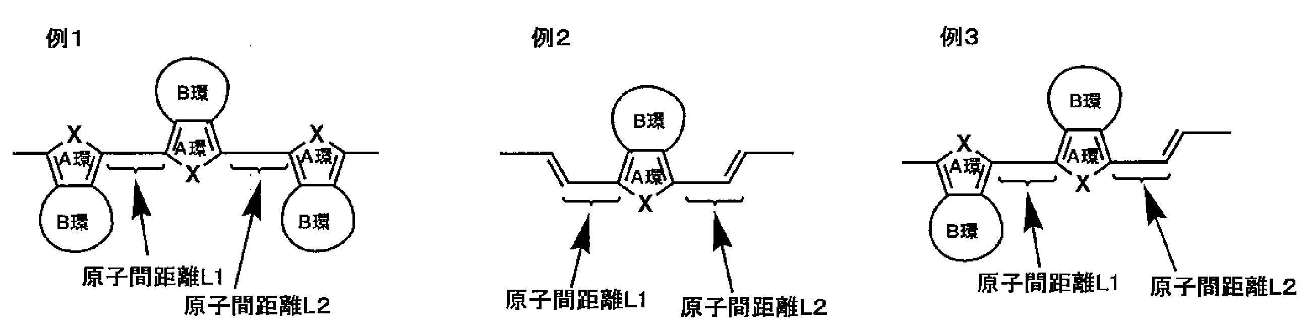
この平均ユニット間距離Lが短くなるほど、A環の結合手で直結する原子間の結合の二重結合性が高まって、A環が後述する擬キノイド型の共鳴構造を形成しやすくなる。
本願発明においては、擬キノイド型の共鳴構造の寄与率を、A環の結合手の原子間距離Lで、規定したものである。
この原子間距離L1およびL2(単位:Å)は、Gaussian計算法(使用プログラム名:Gaussian09(ガウシアン社製)、使用パラメータ:B3LYP/6-31G*)により、最適化された構造から算出できる。なお、高分子化合物の主鎖共役構造を反映させた原子間距離を計算で算出するためには、計算入力用の分子構造として十分な長さの共役長を有すること、すなわち十分な数の繰り返し単位を有することが必要である。具体的には、計算入力用の構造として、原子間距離L1またはL2を算出する結合の両側に、それぞれ少なくとも4個の繰り返し単位が連結していることが必要である。本発明においては、繰り返し単位の連結数が「合計8個」である場合の、計算値を示す。
本願発明においては、擬キノイド型の共鳴構造の寄与率を、A環の結合手の原子間距離Lで、規定したものである。
この原子間距離L1およびL2(単位:Å)は、Gaussian計算法(使用プログラム名:Gaussian09(ガウシアン社製)、使用パラメータ:B3LYP/6-31G*)により、最適化された構造から算出できる。なお、高分子化合物の主鎖共役構造を反映させた原子間距離を計算で算出するためには、計算入力用の分子構造として十分な長さの共役長を有すること、すなわち十分な数の繰り返し単位を有することが必要である。具体的には、計算入力用の構造として、原子間距離L1またはL2を算出する結合の両側に、それぞれ少なくとも4個の繰り返し単位が連結していることが必要である。本発明においては、繰り返し単位の連結数が「合計8個」である場合の、計算値を示す。
本発明において、「~」を用いて表される数値範囲は、「~」の前後に記載される数値を下限値および上限値として含む範囲を意味する。
また、本発明において、置換基に関してxxx基というときには、そのxxx基に任意の置換基を有していてもよい。また、同一の符号で示された基が複数ある場合は、互いに同じであっても異なっていてもよい。
各式で示される繰り返し構造は、まったく同じ繰り返し構造でなくとも、式に示される範囲であれば、異なった繰り返し構造をも含む。例えば、繰り返し構造が置換基としてアルキル基を有する場合、各式で示される繰り返し構造は、メチル基を有する繰り返し構造のみでもよく、メチル基を有する繰り返し構造に加えて、他のアルキル基、例えばエチル基を有する繰り返し構造を含んでいてもよい。
また、本発明において、置換基に関してxxx基というときには、そのxxx基に任意の置換基を有していてもよい。また、同一の符号で示された基が複数ある場合は、互いに同じであっても異なっていてもよい。
各式で示される繰り返し構造は、まったく同じ繰り返し構造でなくとも、式に示される範囲であれば、異なった繰り返し構造をも含む。例えば、繰り返し構造が置換基としてアルキル基を有する場合、各式で示される繰り返し構造は、メチル基を有する繰り返し構造のみでもよく、メチル基を有する繰り返し構造に加えて、他のアルキル基、例えばエチル基を有する繰り返し構造を含んでいてもよい。
本発明の熱電変換材料および熱変換素子は、ナノ導電性材料の分散性が高く、優れた熱電変換性能を発揮する。
また、本発明の熱電変換素子を用いた本発明の熱電発電用物品およびセンサー用電源等は、優れた熱電変換性能を発揮する。
本発明の上記および他の特徴および利点は、下記の記載および添付の図面からより明らかになるであろう。
また、本発明の熱電変換素子を用いた本発明の熱電発電用物品およびセンサー用電源等は、優れた熱電変換性能を発揮する。
本発明の上記および他の特徴および利点は、下記の記載および添付の図面からより明らかになるであろう。
本発明の熱電変換素子は、基材上に、第1の電極、熱電変換層および第2の電極を有する。この熱電変換層は、長軸方向の平均長さが少なくとも5nmであるナノ導電性材料、および、上記式(1)で表される繰り返し単位を有する熱励起高分子化合物(本発明の熱励起高分子化合物)を含有している。この熱電変換層は、上記ナノ導電性材料および上記本発明の熱励起高分子化合物を含有する本発明の熱電変換材料によって、基材上に成形されている。
本発明の熱電変換素子の熱電変換性能は、下記式(A)で示される無次元性能指数ZT(以下、単に性能指数ZTということがある)により表すことができる。
式(A) 性能指数ZT=S2・σ・T/κ
式(A)において、 S(V/K):絶対温度1K当りの熱起電力(ゼーベック係数)
σ(S/m):導電率
κ(W/mK):熱伝導率
T(K):絶対温度
式(A) 性能指数ZT=S2・σ・T/κ
式(A)において、 S(V/K):絶対温度1K当りの熱起電力(ゼーベック係数)
σ(S/m):導電率
κ(W/mK):熱伝導率
T(K):絶対温度
上記式(A)から明らかなように、熱電変換性能の向上には、熱起電力Sおよび導電率σを高めるとともに、熱伝導率κを下げることが重要となる。このように熱電変換性能には、導電率σ以外のファクターが大きく影響するため、一般的に導電率σが高いとされる材料であっても、熱電変換材料として有効に機能するかは実際のところ未知数である。
また、熱電変換素子は、熱電変換層の厚さ方向または面方向に温度差が生じている状態で、厚さ方向または面方向に温度差を伝達するように機能する。したがって、熱電変換材料をある程度の厚みを持った形状に成形して熱電変換層を形成する必要がある。そのため、熱電変換層を塗布により成膜する場合には、熱電変換材料には良好な塗布性や成膜性が要求される。本発明の熱電変換材料は、ナノ導電性材料の分散性が良好で塗布性や成膜性においても優れ、熱電変換層への成形、加工に適する。
以下、本発明の熱電変換材料、次いで本発明の熱電変換素子等について、説明する。
[熱電変換材料]
本発明の熱電変換材料は、熱電変換素子の熱電変換層を形成するための熱電変換組成物であって、長軸方向の平均長さが少なくとも5nmであるナノ導電性材料および上記本発明の熱励起高分子化合物を含有している。
本発明の熱電変換材料は、熱電変換素子の熱電変換層を形成するための熱電変換組成物であって、長軸方向の平均長さが少なくとも5nmであるナノ導電性材料および上記本発明の熱励起高分子化合物を含有している。
まず、本発明の熱電変換材料に用いる各成分について説明する。
<ナノ導電性材料>
本発明に用いるナノ導電性材料は、長軸方向の平均長さが少なくとも5nmであり、導電性を有する材料であればよい。「ナノ」とはナノメートルを意味する。
長軸方向の平均長さは、ナノ導電性材料の非凝集体(例えば一次粒子または分子1個等の凝集していない状態をいう)における長軸方向の長さの平均をいう。この平均長さは、透過型電子顕微鏡(TEM)、走査型電子顕微鏡(SEM)、走査型トンネル顕微鏡(STM)または原子間力顕微鏡(AFM)等の画像解析により、ナノ導電性材料30個の長軸方向の長さを測定し、これらを平均して、求めることができる。
長軸方向の平均長さは、少なくとも5nmであれば特に限定されず、例えば1000μm以下が好ましく、500μm以下がより好ましい。
ナノ導電性材料の長軸方向の平均長さがこのように大きいと後述する本発明の熱励起高分子により分散性が向上する。長軸方向の平均長さが少なくとも5nmの大きなナノ導電性材料が、本発明の熱励起高分子と、π-π相互作用等の分子間相互作用をしやすくなるものと、考えられる。
本発明に用いるナノ導電性材料は、長軸方向の平均長さが少なくとも5nmであり、導電性を有する材料であればよい。「ナノ」とはナノメートルを意味する。
長軸方向の平均長さは、ナノ導電性材料の非凝集体(例えば一次粒子または分子1個等の凝集していない状態をいう)における長軸方向の長さの平均をいう。この平均長さは、透過型電子顕微鏡(TEM)、走査型電子顕微鏡(SEM)、走査型トンネル顕微鏡(STM)または原子間力顕微鏡(AFM)等の画像解析により、ナノ導電性材料30個の長軸方向の長さを測定し、これらを平均して、求めることができる。
長軸方向の平均長さは、少なくとも5nmであれば特に限定されず、例えば1000μm以下が好ましく、500μm以下がより好ましい。
ナノ導電性材料の長軸方向の平均長さがこのように大きいと後述する本発明の熱励起高分子により分散性が向上する。長軸方向の平均長さが少なくとも5nmの大きなナノ導電性材料が、本発明の熱励起高分子と、π-π相互作用等の分子間相互作用をしやすくなるものと、考えられる。
本発明に用いるナノ導電性材料としては、導電性を有する炭素材料(以下、ナノ炭素材料ということがある)、金属材料(以下、ナノ金属材料ということがある)等が挙げられる。
ナノ導電性材料は、ナノ炭素材料およびナノ金属材料の中でも、それぞれ後述する、カーボンナノチューブ(以後、CNTとも称す)、カーボンナノファイバー、グラファイト、グラフェンおよびカーボンナノ粒子のナノ炭素材料、ならびに、金属ナノワイヤーが好ましく、導電性向上および溶媒中での分散性向上の観点で、カーボンナノチューブが特に好ましい。
ナノ導電性材料は、ナノ炭素材料およびナノ金属材料の中でも、それぞれ後述する、カーボンナノチューブ(以後、CNTとも称す)、カーボンナノファイバー、グラファイト、グラフェンおよびカーボンナノ粒子のナノ炭素材料、ならびに、金属ナノワイヤーが好ましく、導電性向上および溶媒中での分散性向上の観点で、カーボンナノチューブが特に好ましい。
熱電変換材料中のナノ導電性材料の含有量は、熱電変換性能の点で、熱電変換材料の全固形分中、2~60質量%が好ましく、5~55質量%がより好ましく、10~50質量%が特に好ましい。
ナノ導電性材料は、1種のみを単独で使用してもよく、2種以上を併用してもよい。ナノ導電性材料として2種以上を併用する場合には、少なくとも1種ずつのナノ炭素材料およびナノ金属材料を併用してもよく、ナノ炭素材料またはナノ金属材料それぞれを2種併用してもよい。
ナノ導電性材料は、1種のみを単独で使用してもよく、2種以上を併用してもよい。ナノ導電性材料として2種以上を併用する場合には、少なくとも1種ずつのナノ炭素材料およびナノ金属材料を併用してもよく、ナノ炭素材料またはナノ金属材料それぞれを2種併用してもよい。
1.ナノ炭素材料
本発明で使用するナノ炭素材料は、上記平均長さの、導電性を有する炭素材料であって、その一例を挙げると、炭素原子のsp2混成軌道で構成される炭素-炭素結合によって炭素原子同士が化学結合してなる導電性材料等である。具体的には、カーボンナノチューブ、カーボンナノチューブの片側が閉じた形をしたカーボンナノホーン、カーボンナノファイバー、カーボンナノウォール、カーボンナノフィラメント、カーボンナノコイル、気相成長カーボン(VGCF)、グラファイト、グラフェン、カーボンナノ粒子、カーボンナノチューブの頭部に穴があいたコップ型のナノカーボン物質等が挙げられる。また、ナノ炭素材料として、グラファイト型の結晶構造を持ち、導電性を示す各種カーボンブラックも用いることができる。例えば、ケッチェンブラック、アセチレンブラック等が挙げられ、具体的には、キャボット社の商品名「バルカン」等のカーボンブラックが挙げられる。
本発明で使用するナノ炭素材料は、上記平均長さの、導電性を有する炭素材料であって、その一例を挙げると、炭素原子のsp2混成軌道で構成される炭素-炭素結合によって炭素原子同士が化学結合してなる導電性材料等である。具体的には、カーボンナノチューブ、カーボンナノチューブの片側が閉じた形をしたカーボンナノホーン、カーボンナノファイバー、カーボンナノウォール、カーボンナノフィラメント、カーボンナノコイル、気相成長カーボン(VGCF)、グラファイト、グラフェン、カーボンナノ粒子、カーボンナノチューブの頭部に穴があいたコップ型のナノカーボン物質等が挙げられる。また、ナノ炭素材料として、グラファイト型の結晶構造を持ち、導電性を示す各種カーボンブラックも用いることができる。例えば、ケッチェンブラック、アセチレンブラック等が挙げられ、具体的には、キャボット社の商品名「バルカン」等のカーボンブラックが挙げられる。
本発明で用いるナノ炭素材料は、長軸方向の平均長さが少なくとも5nmであれば特に限定されない。具体的には、ナノ炭素材料が、カーボンナノチューブ、カーボンナノホーン、カーボンナノファイバー、カーボンナノフィラメント、カーボンナノコイル、気相成長カーボン(VGCF)、コップ型のナノカーボン物質等である場合、特にCNTである場合、長軸方向の平均長さは、製造容易性、成膜性、導電性等の観点から、0.01~1000μmであることが好ましく、0.1~100μmであることがより好ましい。また、平均直径は、特に限定されないが、耐久性、透明性、成膜性、導電性等の観点から、0.4~100nmであることが好ましく、より好ましくは50nm以下、さらに好ましくは15nm以下である。
カーボンナノウォール、グラファイトおよびグラフェンは、長軸方向の平均長さ、すなわち一辺の平均長が、少なくとも5nmであればよい。その上限値は特に限定されないが、例えば、80μmが好ましい。
カーボンナノ粒子は、長軸方向の平均長さとしての平均粒径が少なくとも5nmであればよい。その上限値は特に限定されないが、例えば、200nmが好ましい。
カーボンナノウォール、グラファイトおよびグラフェンは、長軸方向の平均長さ、すなわち一辺の平均長が、少なくとも5nmであればよい。その上限値は特に限定されないが、例えば、80μmが好ましい。
カーボンナノ粒子は、長軸方向の平均長さとしての平均粒径が少なくとも5nmであればよい。その上限値は特に限定されないが、例えば、200nmが好ましい。
ナノ炭素材料は、上述の中でも、カーボンナノチューブ、カーボンナノファイバー、グラファイト、グラフェンおよびカーボンナノ粒子が好ましく、カーボンナノチューブが特に好ましい。
これらのナノ炭素材料は、従来の製造方法によって製造できる。具体的には、二酸化炭素の接触水素還元、アーク放電法、レーザー蒸発法、化学気相成長法(以下、CVD法という)、気相成長法、気相流動法、一酸化炭素を高温高圧化で鉄触媒と共に反応させて気相で成長させるHiPco法、オイルファーネス法等が挙げられる。このようにして製造されたナノ炭素材料は、そのまま用いることもでき、また、洗浄、遠心分離、ろ過、酸化、クロマトグラフ等によって精製されたものを用いることもできる。さらに、ナノ炭素材料は、必要に応じて、ボールミル、振動ミル、サンドミル、ロールミル等のボール型混練装置等を用いて粉砕したもの、化学的、物理的処理によって短く切断されたもの等を用いることもできる。
以下、カーボンナノチューブについて説明する。CNTは、1枚の炭素膜(グラフェン・シート)が円筒状に巻かれた単層CNT、2枚のグラフェン・シートが同心円状に巻かれた2層CNT、および複数のグラフェン・シートが同心円状に巻かれた多層CNTがある。本発明においては、単層CNT、2層CNT、多層CNTを各々単独で用いてもよく、2種以上を併せて用いてもよい。特に、導電性および半導体特性において優れた性質を持つ単層CNTおよび2層CNTを用いることが好ましく、単層CNTを用いることがより好ましい。
単層CNTの場合、グラフェン・シートのグラフェンの六角形の向きに基づく螺旋構造の対称性を軸性カイラルといい、グラフェン上のある6員環の基準点からの2次元格子ベクトルのことをカイラルベクトルという。このカイラルベクトルを指数化した(n,m)をカイラル指数といい、このカイラル指数によって金属性と半導体性に分かれる。具体的には、n-mが3の倍数であるものが金属性を示し、3の倍数でないものが半導体性を示す。
本発明で用いる単層CNTは、半導体性のものであっても、金属性のものであってもよく、両者を併せて用いてもよい。また、CNTには金属等が内包されていてもよい。
単層CNTの場合、グラフェン・シートのグラフェンの六角形の向きに基づく螺旋構造の対称性を軸性カイラルといい、グラフェン上のある6員環の基準点からの2次元格子ベクトルのことをカイラルベクトルという。このカイラルベクトルを指数化した(n,m)をカイラル指数といい、このカイラル指数によって金属性と半導体性に分かれる。具体的には、n-mが3の倍数であるものが金属性を示し、3の倍数でないものが半導体性を示す。
本発明で用いる単層CNTは、半導体性のものであっても、金属性のものであってもよく、両者を併せて用いてもよい。また、CNTには金属等が内包されていてもよい。
CNTはアーク放電法、CVD法、レーザー・アブレーション法等によって製造することができる。本発明に用いられるCNTは、いずれの方法によって得られたものであってもよいが、好ましくはアーク放電法およびCVD法により得られたものである。
CNTを製造する際には、同時にフラーレンやグラファイト、非晶性炭素が副生成物として生じることがある。これら副生成物を除去するために精製してもよい。CNTの精製方法は特に限定されないが、上述の精製法の他に、硝酸、硫酸等による酸処理、超音波処理が不純物の除去には有効である。併せて、フィルターによる分離除去を行うことも、純度を向上させる観点からより好ましい。
CNTを製造する際には、同時にフラーレンやグラファイト、非晶性炭素が副生成物として生じることがある。これら副生成物を除去するために精製してもよい。CNTの精製方法は特に限定されないが、上述の精製法の他に、硝酸、硫酸等による酸処理、超音波処理が不純物の除去には有効である。併せて、フィルターによる分離除去を行うことも、純度を向上させる観点からより好ましい。
精製の後、得られたCNTをそのまま用いることもできる。また、CNTは一般に紐状で得られるため、用途に応じて所望の長さにカットして用いてもよい。CNTは、硝酸、硫酸等による酸処理、超音波処理、凍結粉砕法等により短繊維状にカットすることができる。また、併せてフィルターによる分離を行うことも、純度を向上させる観点から好ましい。
本発明においては、カットしたCNTだけではなく、あらかじめ短繊維状に作製したCNTも同様に使用できる。このような短繊維状CNTは、例えば、基板上に鉄、コバルト等の触媒金属を形成し、その表面にCVD法により700~900℃で炭素化合物を熱分解してCNTを気相成長させることによって、基板表面に垂直方向に配向した形状で得られる。このようにして作製された短繊維状CNTは基板から剥ぎ取る等の方法で取り出すことができる。また、短繊維状CNTはポーラスシリコンのようなポーラスな支持体や、アルミナの陽極酸化膜上に触媒金属を担持させ、その表面にCNTをCVD法にて成長させることもできる。触媒金属を分子内に含む鉄フタロシアニンのような分子を原料とし、アルゴン/水素のガス流中でCVDを行うことによって基板上にCNTを作製する方法でも、配向した短繊維状のCNTを作製することもできる。さらには、エピタキシャル成長法によってSiC単結晶表面に配向した短繊維状CNTを得ることもできる。
本発明においては、カットしたCNTだけではなく、あらかじめ短繊維状に作製したCNTも同様に使用できる。このような短繊維状CNTは、例えば、基板上に鉄、コバルト等の触媒金属を形成し、その表面にCVD法により700~900℃で炭素化合物を熱分解してCNTを気相成長させることによって、基板表面に垂直方向に配向した形状で得られる。このようにして作製された短繊維状CNTは基板から剥ぎ取る等の方法で取り出すことができる。また、短繊維状CNTはポーラスシリコンのようなポーラスな支持体や、アルミナの陽極酸化膜上に触媒金属を担持させ、その表面にCNTをCVD法にて成長させることもできる。触媒金属を分子内に含む鉄フタロシアニンのような分子を原料とし、アルゴン/水素のガス流中でCVDを行うことによって基板上にCNTを作製する方法でも、配向した短繊維状のCNTを作製することもできる。さらには、エピタキシャル成長法によってSiC単結晶表面に配向した短繊維状CNTを得ることもできる。
2.ナノ金属材料
本発明で使用するナノ金属材料は、上記平均長さの、繊維状または粒子状の金属材料等である。具体的には、繊維状の金属材料(金属繊維ともいう)、粒子状の金属材料(金属ナノ粒子ともいう)等が挙げられる。ナノ金属材料は、後述する金属ナノワイヤーが好ましい。
本発明で使用するナノ金属材料は、上記平均長さの、繊維状または粒子状の金属材料等である。具体的には、繊維状の金属材料(金属繊維ともいう)、粒子状の金属材料(金属ナノ粒子ともいう)等が挙げられる。ナノ金属材料は、後述する金属ナノワイヤーが好ましい。
金属繊維は、中実構造または中空構造であるのが好ましい。本発明に用いる金属繊維は、長軸方向の平均長さが少なくとも5nmであればよい。金属繊維のうち、短軸方向の平均長さが1~1,000nmであって長軸方向の平均長さが1~100μmの中実構造を持つ金属繊維を金属ナノワイヤーといい、短軸方向の平均長さが1~1,000nm、長軸方向の平均長さが0.1~1,000μmであって中空構造を持つ金属繊維を金属ナノチューブという。
金属繊維の材料は、導電性を有する金属であればよく、目的に応じて適宜選択することができる。金属繊維の材料は、例えば、長周期律表(国際純正および応用化学連合(IUPAC)、1991改訂)の第4周期、第5周期および第6周期からなる群から選ばれる少なくとも1種の金属が好ましく、第2族~第14族から選ばれる少なくとも1種の金属がより好ましく、第2族、第8族、第9族、第10族、第11族、第12族、第13族、および第14族から選ばれる少なくとも1種の金属がさらに好ましい。
このような金属として、例えば、銅、銀、金、白金、パラジウム、ニッケル、錫、コバルト、ロジウム、イリジウム、鉄、ルテニウム、オスミウム、マンガン、モリブデン、タングステン、ニオブ、タンテル、チタン、ビスマス、アンチモン、鉛、またはこれらの合金等が挙げられる。これらの中でも、導電性に優れる点で、銀、および銀との合金が好ましい。銀との合金で使用する金属としては、白金、オスミウム、パラジウム、イリジウム等が挙げられる。金属は、1種単独で使用してもよく、2種以上を併用してもよい。
このような金属として、例えば、銅、銀、金、白金、パラジウム、ニッケル、錫、コバルト、ロジウム、イリジウム、鉄、ルテニウム、オスミウム、マンガン、モリブデン、タングステン、ニオブ、タンテル、チタン、ビスマス、アンチモン、鉛、またはこれらの合金等が挙げられる。これらの中でも、導電性に優れる点で、銀、および銀との合金が好ましい。銀との合金で使用する金属としては、白金、オスミウム、パラジウム、イリジウム等が挙げられる。金属は、1種単独で使用してもよく、2種以上を併用してもよい。
金属ナノワイヤーは、上述の金属で中空構造に形成されていれば、その形状は特に限定されず、目的に応じて適宜選択することができる。例えば、円柱状、直方体状、断面が多角形となる柱状など任意の形状をとることができる。その形状は、熱電変換層の透明性が高くなる点で、円柱状が好ましく、また、断面の多角形の角が丸まっている断面形状を有することが好ましい。金属ナノワイヤーの断面形状は、透過型電子顕微鏡(TEM)で観察することにより調べることができる。
金属ナノワイヤーの長軸方向の平均長さは、上記ナノ炭素材料と同じ観点から、1μm以上が好ましく、1~40μmがより好ましく、3~35μmがさらに好ましく、5~30μmが特に好ましい。なお、金属ナノワイヤーが曲がっている場合、それを弧とする円を考慮し、その半径および曲率から算出される値を長軸長さとする。
金属ナノワイヤーの短軸方向の平均長さ(「平均短軸径」または「平均直径」と称することがある)は、同様に、50nm以下が好ましく、1~50nmがより好ましく、10~40nmがさらに好ましく、15~35nmが特に好ましい。なお、金属ナノワイヤーの短軸が円形でない場合の短軸長さは、最も長いものを短軸長さとする。
金属ナノワイヤーの短軸方向の平均長さ(「平均短軸径」または「平均直径」と称することがある)は、同様に、50nm以下が好ましく、1~50nmがより好ましく、10~40nmがさらに好ましく、15~35nmが特に好ましい。なお、金属ナノワイヤーの短軸が円形でない場合の短軸長さは、最も長いものを短軸長さとする。
金属ナノワイヤーは、いかなる製造方法で製造してもよいが、特開2012-230881号公報に記載されている、ハロゲン化合物と分散添加剤とを溶解した溶媒中で加熱しながら金属イオンを還元する製造方法で製造するのが好ましい。ハロゲン化合物、分散添加剤および溶媒ならびに加熱条件等の詳細は特開2012-230881号公報に記載されている。また、この製造方法以外にも、例えば、特開2009-215594号公報、特開2009-242880号公報、特開2009-299162号公報、特開2010-84173号公報、特開2010-86714号公報等にそれぞれ記載の製造方法によって、金属ナノワイヤーを製造することもできる。
金属ナノチューブは、上述の金属で中空構造に形成されていれば、その形状は特に限定されず、また単層であっても多層であってもよい。導電性および熱伝導性に優れる点で、金属ナノチューブは単層であるのが好ましい。
金属ナノチューブの厚み(外径と内径との差)は、耐久性、透明性、成膜性、導電性等の観点から、3~80nmが好ましく、3~30nmがより好ましい。金属ナノチューブは、長軸方向の平均長さが少なくとも5nmであればよい。金属ナノチューブの長軸方向の平均長さは、上記ナノ炭素材料と同じ観点から、1~40μmが好ましく、3~35μmがより好ましく、5~30μmがさらに好ましい。金属ナノチューブの短軸方向の平均長さは、金属ナノワイヤーの短軸方向の平均長さと同じであるのが好ましい。
金属ナノチューブの厚み(外径と内径との差)は、耐久性、透明性、成膜性、導電性等の観点から、3~80nmが好ましく、3~30nmがより好ましい。金属ナノチューブは、長軸方向の平均長さが少なくとも5nmであればよい。金属ナノチューブの長軸方向の平均長さは、上記ナノ炭素材料と同じ観点から、1~40μmが好ましく、3~35μmがより好ましく、5~30μmがさらに好ましい。金属ナノチューブの短軸方向の平均長さは、金属ナノワイヤーの短軸方向の平均長さと同じであるのが好ましい。
金属ナノチューブは、いかなる製造方法で製造してもよく、例えば、米国特許出願公開第2005/0056118号明細書に記載の製造方法等で製造することができる。
金属ナノ粒子は、上述の金属で形成された、粒子状または粉末状の金属微粒子であればよく、金属微粒子、金属微粒子の表面を保護剤で被覆したものでもよく、さらに、表面を被覆したものを分散媒体中に分散させたものでもよい。金属ナノ粒子に使用される金属としては、上述した中でも、銀、銅、金、パラジウム、ニッケル、ロジウムなどが好ましく挙げられる。また、これらの少なくとも2種からなる合金、これらの少なくとも1種と鉄との合金等も使用できる。2種からなる合金としては、例えば、白金-金合金、白金-パラジウム合金、金-銀合金、銀-パラジウム合金、パラジウム-金合金、ロジウム-パラジウム合金、銀-ロジウム合金、銅-パラジウム合金、ニッケル-パラジウム合金等が挙げられる。また、鉄との合金としては、例えば、鉄-白金合金、鉄-白金-銅合金、鉄-白金-スズ合金、鉄-白金-ビスマス合金および鉄-白金-鉛合金等が挙げられる。これらの金属または合金は、単独でまたは2種以上組み合わせて用いることができる。
金属ナノ粒子は、長軸方向の平均長さとしての平均粒径が少なくとも5nmであればよく、特に限定されないが、導電性に優れる点で、例えば150nm以下が好ましい。
金属微粒子の保護剤は、例えば、特開2012-222055号公報に記載の保護剤が好適に挙げられる。炭素数10~20の直鎖状または分枝状のアルキル鎖を有する保護剤、特に脂肪酸類または脂肪族アミン類、脂肪族チオール類もしくは脂肪族アルコール類等がさらに好適に挙げられる。ここで、炭素数が10~20であると、金属ナノ粒子の保存安定性が高く、かつ導電性にも優れる。脂肪酸類脂肪族アミン類、脂肪族チオール類および脂肪族アルコール類は、特開2012-222055号公報に記載のものが好適である。
金属ナノ粒子は、いかなる製造方法で製造されてもよく、製造方法として、例えば、ガス中蒸着法、スパッタリング法、金属蒸気合成法、コロイド法、アルコキシド法、共沈法、均一沈殿法、熱分解法、化学還元法、アミン還元法および溶媒蒸発法等が挙げられる。これら製造方法は、それぞれ特有の特徴を備えるが、特に大量生産を目的とする場合には化学還元法、アミン還元法を用いるのが好ましい。これらの製造方法を実施するに当たっては、必要に応じて上述の保護剤を選択して使用するほか、公知の還元剤等を適宜用いることができる。
<熱励起高分子化合物>
本発明に用いる熱励起高分子化合物は、下記式(1)で表される繰り返し単位を有する。
本発明に用いる熱励起高分子化合物は、下記式(1)で表される繰り返し単位を有する。

式(1)中、A環は共役炭化水素環または共役ヘテロ環を表す。Xは、炭素原子、酸素原子、硫黄原子、窒素原子、リン原子およびケイ素原子からなる群より選択される1または2以上の原子をA環の環構成原子とする基を表す。A環の平均ユニット間距離は1.42Å以下である。R11およびR12は各々独立に置換基を表し、互いに連結して環を形成していてもよい。*は繰り返し単位の結合位置を表す。
本発明の熱励起高分子化合物は、下記のように、A環(主鎖)が、環内共役型の共鳴構造(極限構造)と、環外共役である擬キノイド型の極限構造とをとることができる。
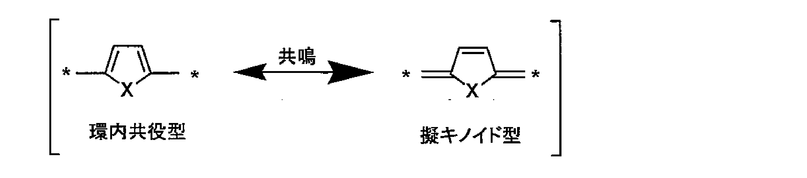
標準的な原子間距離は、炭素-炭素の単結合(C-C)の場合1.54Åであり、炭素-炭素の二重結合(C=C)の場合1.34~1.395Åであることから、本発明の熱励起高分子化合物において、A環の平均ユニット間距離が1.42Å以下であると、環内共役型の共鳴構造よりも擬キノイド型の極限構造が安定化され、その寄与が高くなる。
特に、後述する式(2)で表される繰り返し単位は、A環に芳香族環のB環が縮環しており、擬キノイド型の極限構造がさらに安定化され、その寄与がより高くなると考えられる。
特に、後述する式(2)で表される繰り返し単位は、A環に芳香族環のB環が縮環しており、擬キノイド型の極限構造がさらに安定化され、その寄与がより高くなると考えられる。
このような環内共役型と擬キノイド型の共鳴構造の寄与率は、上記平均ユニット間距離Lによって判断することができる。すなわち、平均ユニット間距離Lが短くなるほど、二重結合性が高まるため、環内共役型の共鳴構造よりも擬キノイド型の共鳴構造の方が安定化されていると判断することができる。この二重結合性の増加により、主鎖を形成する結合の自由回転が抑えられ、主鎖の平面性が高くなる。また、本発明において、A環の平均ユニット間距離Lが1.42Å以下である場合、光学バンドギャップが低下する傾向がある。
逆に、平均ユニット間距離Lが長くなるほど、単結合性(一重結合性)が高まるため、環内共役型の共鳴構造の方が安定化されていると判断することができる。平均ユニット間距離Lが1.42Åよりも長い場合、擬キノイド構造の寄与が小さくなり、光学バンドギャップが増加する傾向がある。
本発明において、A環の平均ユニット間距離Lは、1.42Å以下であればよく、1.41Å以下が好ましく、1.40Å以下がより好ましい。
擬キノイド型の極限構造においては、主鎖方向に共役が伸びることから、この共役鎖を通じてキャリアが分子内で動きやすく、また主鎖の平面性が向上するため分子間でのπ軌道の重なりが大きくなり、分子間でのキャリアホッピングが促進される。このように分子内および分子間の両方でキャリアが動きやすくなるため、キャリア移動度が向上すると考えられており、この擬キノイド型の極限構造の寄与が大きくなるほどキャリア移動度はさらに向上する。加えて、本発明の熱励起高分子化合物はナノ導電性材料に吸着しやすく、本発明の熱励起高分子化合物とナノ導電性材料とのキャリア輸送経路が密に形成される。その結果、本発明の熱励起高分子化合物で発生した熱励起キャリアが吸着したナノ導電性材料に移動しやすく、キャリアの拡散性が向上して、導電率も増大するため、熱電変換性能が向上すると考えられる。
本発明では、光学バンドギャップは、0.1eV以上1.1eV以下が好ましく、0.1eV以上1.0eV以下がより好ましく、0.1eV以上0.9eV以下がさらに好ましい。
ここで、光学バンドギャップとは、禁制帯のことであり、価電子帯(バンド構造における電子に占有された最も高いエネルギーバンド)の頂上から、伝導帯(電子が空の最も低いエネルギーバンド)の底までのエネルギー準位およびエネルギー差である。
本発明において、光学バンドギャップとは、本発明の熱励起高分子化合物の吸収スペクトルの長波長側の吸収端により定まるものをいい、具体的には、下記式(B)により求められる。
式(B) 光学バンドギャップ(eV)=1240/吸収長波長端(nm)
本発明において、光学バンドギャップとは、本発明の熱励起高分子化合物の吸収スペクトルの長波長側の吸収端により定まるものをいい、具体的には、下記式(B)により求められる。
式(B) 光学バンドギャップ(eV)=1240/吸収長波長端(nm)
式(B)において、吸収長波長端は、吸収スペクトルにおける長波長側の吸収端の波長(nm)をいう。吸収スペクトルは、分光光度計により測定できる。
具体的には、本発明の熱励起高分子化合物を可溶性の有機溶媒に溶解させ、石英基板上に塗布し成膜する。この塗布膜の吸収スペクトルを分光光度計で測定する。吸光度の極大値(λmax)に対し、吸光度が5%となる長波長側の吸収端の波長λ5(単位:nm)を求める。求めたλ5を吸収長波長端として、式(B)から光学バンドギャップ(単位:eV)を算出する。分光光度計としては、紫外可視近赤外(UV-Vis-NIR)分光光度計等を用いることができる。
具体的には、本発明の熱励起高分子化合物を可溶性の有機溶媒に溶解させ、石英基板上に塗布し成膜する。この塗布膜の吸収スペクトルを分光光度計で測定する。吸光度の極大値(λmax)に対し、吸光度が5%となる長波長側の吸収端の波長λ5(単位:nm)を求める。求めたλ5を吸収長波長端として、式(B)から光学バンドギャップ(単位:eV)を算出する。分光光度計としては、紫外可視近赤外(UV-Vis-NIR)分光光度計等を用いることができる。
熱電変換性能の向上には、熱励起確率を向上させ、熱励起子の発生量(熱励起キャリア量)を増やすことが有効である。しかしながら、熱電変換に用いる熱エネルギーは、光エネルギーに比べて小さいため、熱励起子の発生量が十分でないことがある。
本発明の熱励起高分子化合物は、擬キノイド型の極限構造の寄与が大きく、低い光学バンドギャップを有することから、熱励起確率が向上し、しかもより少ない熱量であっても熱励起しやすくなる。その結果、熱電変換素子の高温側における熱励起キャリア量が増加し、熱起電力(ゼーベック係数)が増大して、熱電変換性能が向上すると考えられる。
さらに、本発明の熱励起高分子化合物をナノ導電性材料とともに用いると、本発明の熱励起高分子化合物がナノ導電性材料の分散バインダーとしても機能し、ナノ導電性材料の分散性が向上する。
本発明の熱励起高分子化合物は、平面性の高い擬キノイド型の極限構造の寄与が大きく、これにより、ナノ導電性材料と、π-π相互作用等の分子間相互作用により、吸着しやすくなるものと考えられる。
本発明の熱励起高分子化合物は、平面性の高い擬キノイド型の極限構造の寄与が大きく、これにより、ナノ導電性材料と、π-π相互作用等の分子間相互作用により、吸着しやすくなるものと考えられる。
このように、本発明の熱励起高分子化合物は、上記ナノ導電性材料と併用することにより、熱起電力と導電率とが向上し、その結果、熱電変換性能がより一層向上すると考えられる。
熱電変換材料の全固形分中の、本発明の熱励起高分子化合物の含有率は、熱電変換性能の点から、ナノ導電性材料100質量部に対して、50~2000質量部が好ましく、80~600質量部がより好ましい。
本発明の熱電変換材料には、本発明の熱励起高分子化合物を1種単独で使用してもよく、2種以上を併用してもよい。
本発明の熱電変換材料には、本発明の熱励起高分子化合物を1種単独で使用してもよく、2種以上を併用してもよい。
本発明の熱励起高分子化合物は、上記式(1)で表される繰り返し単位を有し、この繰り返し単位を有してなる主鎖はπ電子または孤立電子対で共役する共役高分子である。
以下、上記式(1)で表される繰り返し単位を詳細に説明する。
以下、上記式(1)で表される繰り返し単位を詳細に説明する。
この繰り返し単位のA環は、ナノ導電性材料との相互作用(吸着性)の観点およびポリマーの導電性の観点で、共役ヘテロ環が好ましい。
Xは、炭素原子、硫黄原子、窒素原子、リン原子およびケイ素原子からなる群より選択される1つの原子を環構成原子とする基であるのが好ましく、炭素原子、硫黄原子および窒素原子からなる群より選択される1つの原子を環構成原子とする基がより好ましい。
Xにおいて、これらの原子は、原子の価数により、水素原子または置換基を有する。この置換基を構成する原子は、特に限定されず、炭素原子、酸素原子、硫黄原子、窒素原子、リン原子、水素原子、ホウ素原子、ケイ素原子、セレン原子等が挙げられる。すなわち、Xは、環構成原子と、これに結合する置換基または水素原子とを有している。
Xにおいて、これらの原子は、原子の価数により、水素原子または置換基を有する。この置換基を構成する原子は、特に限定されず、炭素原子、酸素原子、硫黄原子、窒素原子、リン原子、水素原子、ホウ素原子、ケイ素原子、セレン原子等が挙げられる。すなわち、Xは、環構成原子と、これに結合する置換基または水素原子とを有している。
Xとして、例えば、-Y(=O)m-、-Y(=S)-、-YRx
m-、-Y(=CRx
2)-、-Y(―OH)m-、-Y(―OR)m-、-Y(―SR)m-等の基が挙げられ、これら基を2つ以上組み合わせた基、これら基と-O-とを組み合わせた基が挙げられる。中でも、-Y(=O)m-、-YRx
m-、-Y(=CRx
2)-、および、これら基を2つ以上組み合わせた基が好ましく、-Y(=O)m-、-YRx
m-、-Y(=CRx
2)-、-Y(=O)-Y(=O)-および-YRx
m-YRx
m-がさらに好ましい。ここで、YはXの環構成原子と同義であり、好ましい範囲も同じであり、Rxは水素原子または置換基である。mは1以上の整数であり、Yの原子価に応じて選択され、好ましくは1または2である。
Xは、具体的には、-C(=O)-、-C(=S)-、-CRx
2-、-C(=CRx
2)-、-S(=O)-、-S(=O)2-、-N(→O)-(-N(=O)-とも表記する)、-P(=O)R-、-PR-、―P(OR)3―、―SiR2-、―Si(OR)2-、―SiR2-SiR2-等の基が挙げられ、これら基を2つ以上組み合わせた基、または、これら基と-O-とを組み合わせた基が挙げられる。中でも、Xは、-C(=O)-、-CRx
2-、-C(=CRx
2)-、-C(=O)-C(=O)-、-CRx
2-CRx
2-、-S(=O)-、-S(=O)2-、-N(→O)-が好ましい。
Xが有する置換基および置換基Rxは、特に限定されず、後述する置換基Wが挙げられる。中でも、アルキル基またはアリール基が好ましい。
アルキル基は、直鎖、分岐、環状のいずれでもよく、直鎖アルキル基が好ましい。アルキル基の炭素原子数は、1~20が好ましく、1~10がより好ましく、置換基Wで例示する基が挙げられる。
アリール基は、炭素数6~12のアリール基が好ましく、例えば、フェニルが挙げられる。
アルキル基は、直鎖、分岐、環状のいずれでもよく、直鎖アルキル基が好ましい。アルキル基の炭素原子数は、1~20が好ましく、1~10がより好ましく、置換基Wで例示する基が挙げられる。
アリール基は、炭素数6~12のアリール基が好ましく、例えば、フェニルが挙げられる。
このような基を有するA環は、特に限定されないが、5~7員環が好ましく、5員環または6員環がさらに好ましい。
A環の環構造(置換基R11およびR12を除く)は、下記式(3)~(8)で表されるのが好ましい。各式において、*は繰り返し単位としてのA環の結合位置を表す。
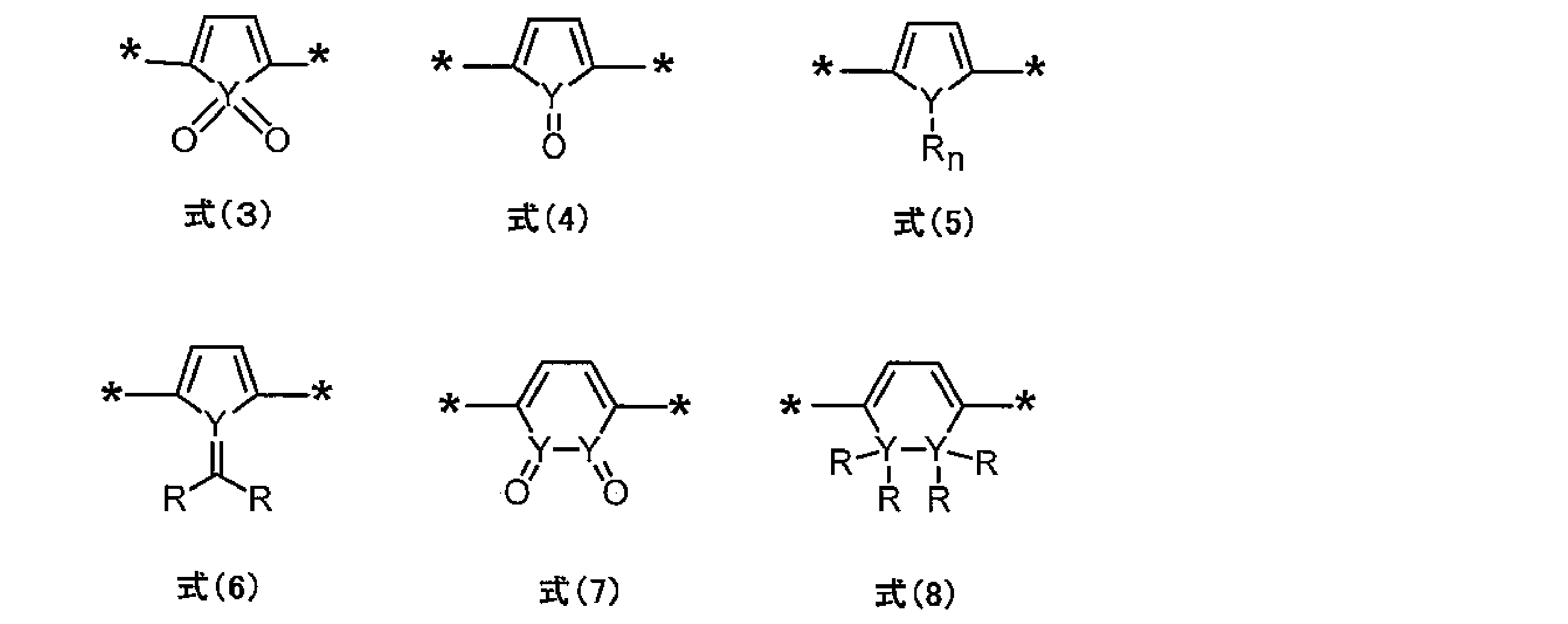
式(3)~式(8)において、Yは、各々独立に、炭素原子、硫黄原子、窒素原子、リン原子およびケイ素原子からなる群より選択される原子を表す。式(7)および(8)における2つのYは同一でも異なっていてもよい。なお、Yは各式におけるYの原子価を満たすように選択される。例えば、式(3)において炭素原子は選択されない。
式(3)~式(8)において、Yは、具体的に例示した上記の好ましいXに対応するように、上記群から原子が選択される。好ましくは、式(3)においてYは硫黄原子であり、式(4)においてYは炭素原子、硫黄原子または窒素原子であり、式(5)においてYは炭素原子、リン原子またはケイ素原子であり、式(6)~式(8)各々においてYは炭素原子である。
式(3)~式(8)において、Yは、具体的に例示した上記の好ましいXに対応するように、上記群から原子が選択される。好ましくは、式(3)においてYは硫黄原子であり、式(4)においてYは炭素原子、硫黄原子または窒素原子であり、式(5)においてYは炭素原子、リン原子またはケイ素原子であり、式(6)~式(8)各々においてYは炭素原子である。
Rは、アルキル基またはアリール基を表し、上記置換基Rxのアルキル基またはアリール基と同義であり、好ましい範囲も同じである。式(5)においてnが2以上の整数である場合ならびに式(6)および式(8)における複数のRは同一でも異なっていてもよい。
nは、1以上の整数を表し、Yの原子価に応じて選択される。Yが炭素原子である場合は2である。
nは、1以上の整数を表し、Yの原子価に応じて選択される。Yが炭素原子である場合は2である。
式(1)において、R11およびR12は、各々独立に、置換基を表す。この置換基は、特に限定されず、後述する置換基Wが挙げられるが、熱電変換特性および分散性の点で、互いに連結して環を形成するものが好ましく、芳香環を形成するものがさらに好ましい。この場合、式(1)で表される繰り返し構造は、下記式(2)で表されるのが好ましい。

式(2)において、A環およびXは式(1)のA環およびXと同義であり、好ましい範囲も同じである。A環の平均ユニット間距離も式(1)のA環と同義であり、好ましい範囲も同じである。*は繰り返し単位の結合位置を表す。
式(2)において、B環は芳香環を表す。B環は、芳香族炭化水素環であっても芳香族ヘテロ環であってもよく、ベンゼン環または5員もしくは6員の芳香族ヘテロ環が好ましい。
芳香族炭化水素環としては、芳香族性を有する単環の炭化水素環であればよく、その基本となる環としてベンゼン環が挙げられる。
芳香族ヘテロ環としては、芳香族性を有する単環のヘテロ環であれば特に限定されないが、5員環の芳香族ヘテロ環または6員環の芳香族ヘテロ環が好適に挙げられる。ヘテロ環を構成するヘテロ原子としては、硫黄原子、窒素原子、酸素原子、ケイ素原子、セレン原子等が挙げられ、酸素原子、硫黄原子、窒素原子が好ましく、硫黄原子、窒素原子がより好ましい。5員環の芳香族ヘテロ環としては、例えば、チオフェン環、フラン環、ピロール環、セレノフェン環、イミダゾール環、ピラゾール環、オキサゾール環、イソオキサゾール環、チアゾール環、イソチアゾール環、トリアゾール環、チアジアゾール環、ジアゾール環、ピリジン環、ピラジン環が挙げられる。6員環の芳香族ヘテロ環としては、例えば、ピリジン環、ピリミジン環、ピリダジン環、ピラジン環、トリアジン環が挙げられる。中でも、熱電変換性能および分散性の点で、チオフェン環、ピロール環、イミダゾール環、ピラゾール環、チアジアゾール環、ジアゾール環、ピリジン環、ピラジン環がさらに好ましい。
B環は、ベンゼン環または5員もしくは6員の芳香族ヘテロ環が好ましい。
B環は、ベンゼン環または5員もしくは6員の芳香族ヘテロ環が好ましい。
B環は、縮環していてもよく、また置換基を有していてもよい。
B環に縮環する環は、脂肪族環であっても芳香族環であってもよく、また炭化水素環であってもヘテロ環であってもよい。なかでも、芳香族環構造を含む環が好ましく、芳香族へテロ環構造を含む環がより好ましい。B環に縮合する環を構成する芳香族炭化水素環、芳香族へテロ環としては、上述の芳香族炭化水素環、芳香族へテロ環が挙げられ、好ましい範囲も同様である。B環に縮環する環の数は、特に限定されないが、1個または2個であるのが好ましい。
B環に縮環する環は、脂肪族環であっても芳香族環であってもよく、また炭化水素環であってもヘテロ環であってもよい。なかでも、芳香族環構造を含む環が好ましく、芳香族へテロ環構造を含む環がより好ましい。B環に縮合する環を構成する芳香族炭化水素環、芳香族へテロ環としては、上述の芳香族炭化水素環、芳香族へテロ環が挙げられ、好ましい範囲も同様である。B環に縮環する環の数は、特に限定されないが、1個または2個であるのが好ましい。
B環が有する置換基は、特に限定されず、後述する置換基Wが挙げられる。中でも、アルキル基(特に炭素数1~30)、アルケニル基(特に炭素数1~26)、アルコキシ基(特に炭素数1~26)、アルキルチオ基(特に炭素数1~26)、アルコキシカルボニル基(特に炭素数1~26)、芳香族炭化水素環基、芳香族ヘテロ環基が好ましい。
上記熱励起高分子化合物は、繰り返し単位として、式(1)または式(2)で表される繰り返し単位を少なくとも1つ有していればよく、複数有していてもよい。
また、繰り返し単位として、式(1)または式(2)で表される繰り返し単位と、式(1)または式(2)で表される繰り返し単位以外の繰り返し単位であって主鎖の共役系を形成可能な別の繰り返し単位とを有する共重合体であってもよい。このような繰り返し単位は1つであっても複数であってもよい。
なお、複数の繰り返し単位を有する場合には、共重合様式は、特に限定されず、ブロック共重合、交互共重合、ランダム共重合、グラフト共重合のいずれでもよい。
また、繰り返し単位として、式(1)または式(2)で表される繰り返し単位と、式(1)または式(2)で表される繰り返し単位以外の繰り返し単位であって主鎖の共役系を形成可能な別の繰り返し単位とを有する共重合体であってもよい。このような繰り返し単位は1つであっても複数であってもよい。
なお、複数の繰り返し単位を有する場合には、共重合様式は、特に限定されず、ブロック共重合、交互共重合、ランダム共重合、グラフト共重合のいずれでもよい。
上記別の繰り返し単位は、主鎖の共役系を形成可能な連結基、原子またはこれらを組合せたものであればよい。このような別の繰り返し単位は、特に限定されないが、エテニレン基、エチニレン基、アリーレン基およびヘテロアリーレン基からなる群より選択される少なくとも1種の繰り返し単位が好ましい。
アリーレン基の炭素数は6~20が好ましく、6~15がより好ましい。アリーレン基は好ましくはフェニレン、ナフチレンである。
アリーレン基は、主鎖の共役系を形成可能な原子、好ましくは窒素原子に結合した複数の芳香環を有し、異なる芳香環で主鎖に結合する基を含む。このような基として、例えば、異なるフェニル基で主鎖に結合する、トリフェニルアミンから得られる2価の基が挙げられる。
アリーレン基は、主鎖の共役系を形成可能な原子、好ましくは窒素原子に結合した複数の芳香環を有し、異なる芳香環で主鎖に結合する基を含む。このような基として、例えば、異なるフェニル基で主鎖に結合する、トリフェニルアミンから得られる2価の基が挙げられる。
また、ヘテロアリーレン基の炭素数は3~20が好ましく、5~12がより好ましい。ヘテロアリーレン基を構成するヘテロ環は、特に限定されないが、5員環または6員環が好ましい。ヘテロ環を構成するヘテロ原子としては、特に限定されないが、硫黄原子、窒素原子、酸素原子、ケイ素原子、セレン原子等が好適に挙げられる。ヘテロアリーレン基の好ましい例としては、2価のチオフェン環、2価のチアゾール環、2価のオキサゾール環、2価のフラン環、2価のピロール環、2価のセレノフェン環、2価のチアゾール環、2価のオキサゾール環、2価のホスホール環、2価のホスホリン環、2価のチアジアゾール環、2価のオキサジアゾール環、2価のピラゾール環、2価のイミダゾール環、2価のピリジン環、2価のピラジン環、2価のピリダジン環、2価のトリアジン環、2価のトリアゾール環、2価のテトラジン環が挙げられる。
アリーレン基およびヘテロアリーレン基は、それぞれ、縮環していてもよく、これらに縮環する環はB環に縮環する上記環と同義であり、好ましい範囲も同じである。縮環したアリーレン基またはヘテロアリーレン基となるものとしては、例えば、フルオレン、ジチエノシロール、シクロペンタジチオフェン、ベンゾジチオフェン、チエノ[3,4-b]チオフェン、[1]ベンゾチエノ[3,2-b][1]ベンゾチオフェン、ベンゾフルオレン等が挙げられる。なお、アリーレン基およびヘテロアリーレン基が縮環している場合に、主鎖と連結する連結位置は、同一の環を構成する環構成原子であっても、異なる環を構成する環構成原子であってもよい。
別の繰り返し単位は置換基を有していてもよい。別の繰り返し単位が有していてもよい置換基はB環が有していてもよい上記置換基と同義であり、好ましい範囲も同じである。
置換基Wとしては、下記の基が挙げられる。
アルキル基(例えば、メチル、エチル、プロピル、イソプロピル、tert-ブチル、ペンチル、ヘキシル、オクチル、ドデシル、トリデシル、テトラデシル、ペンタデシル等)、シクロアルキル基(例えば、シクロペンチル、シクロヘキシル等)、アルケニル基(例えば、ビニル、アリル等)、アルキニル基(例えば、エチニル、プロパルギル等)、芳香族炭化水素環基(芳香族炭素環、アリール等ともいい、例えば、フェニル、p-クロロフェニル、メシチル、トリル、キシリル、ナフチル、アントリル、アズレニル、アセナフテニル、フルオレニル、フェナントリル、インデニル、ピレニル、ビフェニリル等)、芳香族へテロ環基(5または6員環の芳香族へテロ環基が好ましく、また環構成ヘテロ原子は、硫黄原子、窒素原子、酸素原子、ケイ素原子、ホウ素、セレン原子が好ましく、例えば、ピリジル、ピリミジニル、フリル、ピロリル、イミダゾリル、ベンゾイミダゾリル、ピラゾリル、ピラジニル、トリアゾリル(例えば、1,2,4-トリアゾール-1-イル、1,2,3-トリアゾール-1-イル等)、オキサゾリル、ベンゾオキサゾリル、チアゾリル、イソオキサゾリル、イソチアゾリル、フラザニル、チエニル、キノリル、ベンゾフリル、ジベンゾフリル、ベンゾチエニル、ジベンゾチエニル、インドリル、カルバゾリル、カルボリニル、ジアザカルバゾリル(上記カルボリニル基のカルボリン環を構成する炭素原子の一つが窒素原子で置き換わったものを示す)、キノキサリニル、ピリダジニル、トリアジニル、キナゾリニル、フタラジニル、ボロール、アザボリン等)、ヘテロ環基(芳香族でないヘテロ環基で、飽和環であっても不飽和環であってもよく、5または6員環が好ましく、また環構成ヘテロ原子は、硫黄原子、窒素原子、酸素原子、ケイ素原子、セレン原子が好ましく、例えば、ピロリジル、イミダゾリジル、モルホリル、オキサゾリジル等)、アルコキシ基(例えば、メトキシ、エトキシ、プロピルオキシ、ペンチルオキシ、ヘキシルオキシ、オクチルオキシ、ドデシルオキシ等)、シクロアルコキシ基(例えば、シクロペンチルオキシ、シクロヘキシルオキシ等)、アリールオキシ基(例えば、フェノキシ、ナフチルオキシ等)、アルキルチオ基(例えば、メチルチオ、エチルチオ、プロピルチオ、ペンチルチオ、ヘキシルチオ、オクチルチオ、ドデシルチオ等)、シクロアルキルチオ基(例えば、シクロペンチルチオ、シクロヘキシルチオ等)、アリールチオ基(例えば、フェニルチオ、ナフチルチオ等)、アルコキシカルボニル基(例えば、メチルオキシカルボニル、エチルオキシカルボニル、ブチルオキシカルボニル、オクチルオキシカルボニル、ドデシルオキシカルボニル等)、アリールオキシカルボニル基(例えば、フェニルオキシカルボニル、ナフチルオキシカルボニル等)、スルファモイル基(例えば、アミノスルホニル、メチルアミノスルホニル、ジメチルアミノスルホニル、ブチルアミノスルホニル、ヘキシルアミノスルホニル、シクロヘキシルアミノスルホニル、オクチルアミノスルホニル、ドデシルアミノスルホニル、フェニルアミノスルホニル、ナフチルアミノスルホニル、2-ピリジルアミノスルホニル等)、
アルキル基(例えば、メチル、エチル、プロピル、イソプロピル、tert-ブチル、ペンチル、ヘキシル、オクチル、ドデシル、トリデシル、テトラデシル、ペンタデシル等)、シクロアルキル基(例えば、シクロペンチル、シクロヘキシル等)、アルケニル基(例えば、ビニル、アリル等)、アルキニル基(例えば、エチニル、プロパルギル等)、芳香族炭化水素環基(芳香族炭素環、アリール等ともいい、例えば、フェニル、p-クロロフェニル、メシチル、トリル、キシリル、ナフチル、アントリル、アズレニル、アセナフテニル、フルオレニル、フェナントリル、インデニル、ピレニル、ビフェニリル等)、芳香族へテロ環基(5または6員環の芳香族へテロ環基が好ましく、また環構成ヘテロ原子は、硫黄原子、窒素原子、酸素原子、ケイ素原子、ホウ素、セレン原子が好ましく、例えば、ピリジル、ピリミジニル、フリル、ピロリル、イミダゾリル、ベンゾイミダゾリル、ピラゾリル、ピラジニル、トリアゾリル(例えば、1,2,4-トリアゾール-1-イル、1,2,3-トリアゾール-1-イル等)、オキサゾリル、ベンゾオキサゾリル、チアゾリル、イソオキサゾリル、イソチアゾリル、フラザニル、チエニル、キノリル、ベンゾフリル、ジベンゾフリル、ベンゾチエニル、ジベンゾチエニル、インドリル、カルバゾリル、カルボリニル、ジアザカルバゾリル(上記カルボリニル基のカルボリン環を構成する炭素原子の一つが窒素原子で置き換わったものを示す)、キノキサリニル、ピリダジニル、トリアジニル、キナゾリニル、フタラジニル、ボロール、アザボリン等)、ヘテロ環基(芳香族でないヘテロ環基で、飽和環であっても不飽和環であってもよく、5または6員環が好ましく、また環構成ヘテロ原子は、硫黄原子、窒素原子、酸素原子、ケイ素原子、セレン原子が好ましく、例えば、ピロリジル、イミダゾリジル、モルホリル、オキサゾリジル等)、アルコキシ基(例えば、メトキシ、エトキシ、プロピルオキシ、ペンチルオキシ、ヘキシルオキシ、オクチルオキシ、ドデシルオキシ等)、シクロアルコキシ基(例えば、シクロペンチルオキシ、シクロヘキシルオキシ等)、アリールオキシ基(例えば、フェノキシ、ナフチルオキシ等)、アルキルチオ基(例えば、メチルチオ、エチルチオ、プロピルチオ、ペンチルチオ、ヘキシルチオ、オクチルチオ、ドデシルチオ等)、シクロアルキルチオ基(例えば、シクロペンチルチオ、シクロヘキシルチオ等)、アリールチオ基(例えば、フェニルチオ、ナフチルチオ等)、アルコキシカルボニル基(例えば、メチルオキシカルボニル、エチルオキシカルボニル、ブチルオキシカルボニル、オクチルオキシカルボニル、ドデシルオキシカルボニル等)、アリールオキシカルボニル基(例えば、フェニルオキシカルボニル、ナフチルオキシカルボニル等)、スルファモイル基(例えば、アミノスルホニル、メチルアミノスルホニル、ジメチルアミノスルホニル、ブチルアミノスルホニル、ヘキシルアミノスルホニル、シクロヘキシルアミノスルホニル、オクチルアミノスルホニル、ドデシルアミノスルホニル、フェニルアミノスルホニル、ナフチルアミノスルホニル、2-ピリジルアミノスルホニル等)、
アシル基(例えば、アセチル、エチルカルボニル、プロピルカルボニル、ペンチルカルボニル、シクロヘキシルカルボニル、オクチルカルボニル、2-エチルヘキシルカルボニル、ドデシルカルボニル、アクリロイル、メタクリロイル、フェニルカルボニル、ナフチルカルボニル、ピリジルカルボニル等)、アシルオキシ基(例えば、アセチルオキシ、エチルカルボニルオキシ、ブチルカルボニルオキシ、オクチルカルボニルオキシ、ドデシルカルボニルオキシ、フェニルカルボニルオキシ等)、アミド基(例えば、メチルカルボニルアミノ、エチルカルボニルアミノ、ジメチルカルボニルアミノ、プロピルカルボニルアミノ、ペンチルカルボニルアミノ、シクロヘキシルカルボニルアミノ、2-エチルヘキシルカルボニルアミノ、オクチルカルボニルアミノ、ドデシルカルボニルアミノ、フェニルカルボニルアミノ、ナフチルカルボニルアミノ等)、カルバモイル基(例えば、アミノカルボニル、メチルアミノカルボニル、ジメチルアミノカルボニル、プロピルアミノカルボニル、ペンチルアミノカルボニル、シクロヘキシルアミノカルボニル、オクチルアミノカルボニル、2-エチルヘキシルアミノカルボニル、ドデシルアミノカルボニル、フェニルアミノカルボニル、ナフチルアミノカルボニル、2-ピリジルアミノカルボニル等)、ウレイド基(例えば、メチルウレイド、エチルウレイド、ペンチルウレイド、シクロヘキシルウレイド、オクチルウレイド、ドデシルウレイド、フェニルウレイド、ナフチルウレイド、2-ピリジルアミノウレイド等)、スルフィニル基(例えば、メチルスルフィニル、エチルスルフィニル、ブチルスルフィニル、シクロヘキシルスルフィニル、2-エチルヘキシルスルフィニル、ドデシルスルフィニル、フェニルスルフィニル、ナフチルスルフィニル、2-ピリジルスルフィニル等)、アルキルスルホニル基(例えば、メチルスルホニル、エチルスルホニル、ブチルスルホニル、シクロヘキシルスルホニル、2-エチルヘキシルスルホニル、ドデシルスルホニル等)、アリールスルホニル基またはヘテロアリールスルホニル基(例えば、フェニルスルホニル、ナフチルスルホニル、2-ピリジルスルホニル等)、アミノ基(アミノ基、アルキルアミノ基、アルケニルアミノ基、アリールアミノ基、ヘテロ環アミノ基を含み、例えば、アミノ、エチルアミノ、ジメチルアミノ、ブチルアミノ、シクロペンチルアミノ、2-エチルヘキシルアミノ、ドデシルアミノ、アニリノ、ナフチルアミノ、2-ピリジルアミノ等)、シアノ基、ニトロ基、ヒドロキシ基、メルカプト基、シリル基(例えば、トリメチルシリル、トリイソプロピルシリル、トリフェニルシリル、フェニルジエチルシリル等)等が挙げられる。
これらの各基は、さらに置換基を有していてもよく、この置換基としては上記の置換基が挙げられる。例えば、アルキル基にアリール基が置換したアラルキル基、アルキル基にヒドロキシ基が置換したヒドロキシアルキル基等が挙げられる。
これらの各基は、さらに置換基を有していてもよく、この置換基としては上記の置換基が挙げられる。例えば、アルキル基にアリール基が置換したアラルキル基、アルキル基にヒドロキシ基が置換したヒドロキシアルキル基等が挙げられる。
以下に、熱励起高分子化合物の具体例を示すが、本発明はこれらに限定されるものではない。下記に示す熱励起高分子化合物は下記に示す繰り返し単位からなる。実施例にて用いていない化合物の、上記計算法による平均ユニット間距離Lを繰り返し単位の下方に示す。なお、「Ph」はフェニル基を表す。
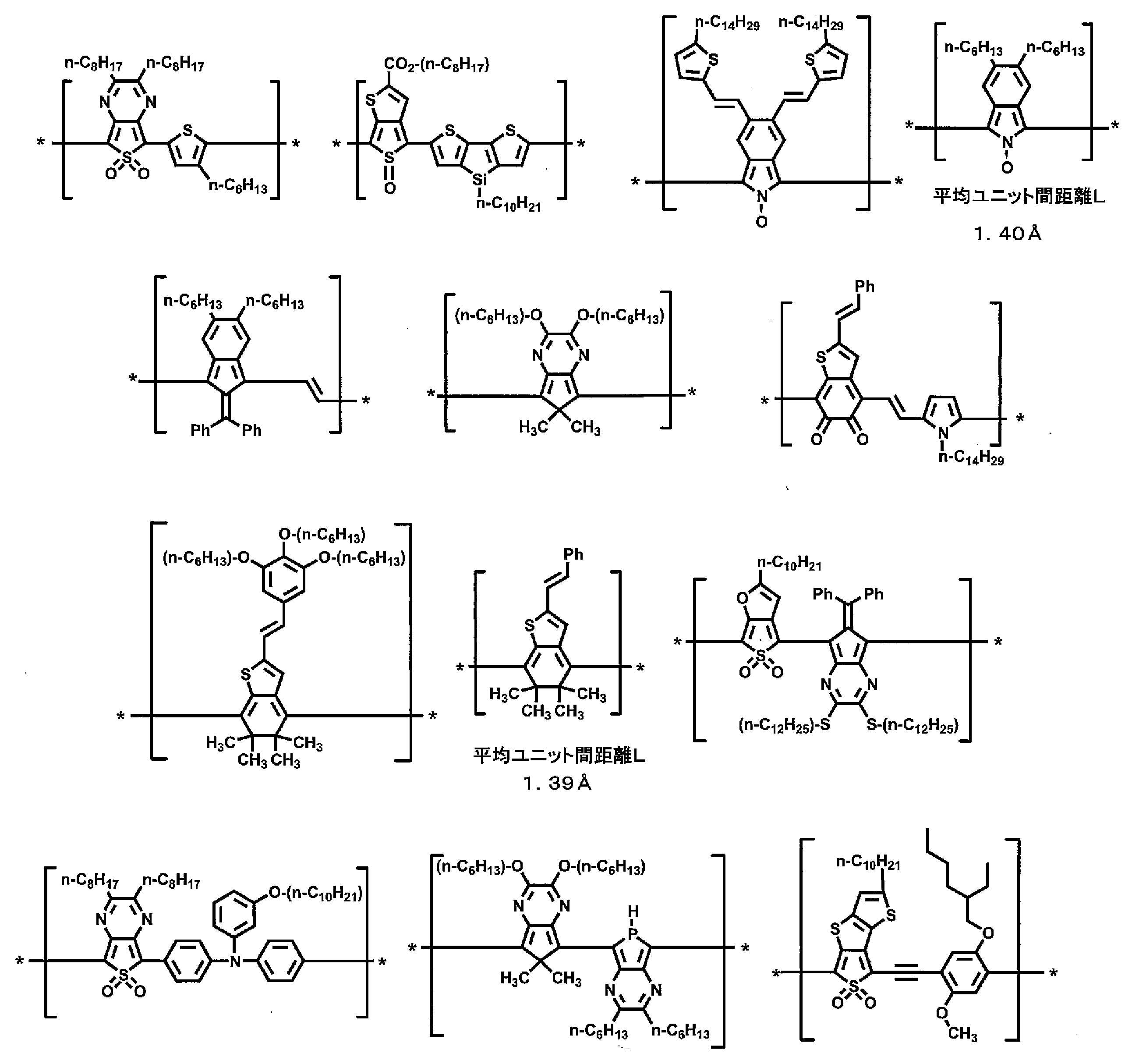
熱励起高分子化合物は、重量平均分子量が5000~30万が好ましく、1万~20万がより好ましい。
重量平均分子量は、ゲル浸透クロマトグラフィー(GPC)により測定できる。例えば、装置:「Alliance GPC2000(Waters社製)」、カラム:TSKgel GMH6-HT×2+TSKgel GMH6-HTL×2(いずれも7.5mmI.D.×30cm、東ソー社製)、カラム温度:140℃、検出器:示差屈折率計、移動相:溶媒(例えばo-ジクロロベンゼン)の構成・条件にて行い、分子量の構成は標準ポリスチレンを用いて平均分子量を求めることができる。
重量平均分子量は、ゲル浸透クロマトグラフィー(GPC)により測定できる。例えば、装置:「Alliance GPC2000(Waters社製)」、カラム:TSKgel GMH6-HT×2+TSKgel GMH6-HTL×2(いずれも7.5mmI.D.×30cm、東ソー社製)、カラム温度:140℃、検出器:示差屈折率計、移動相:溶媒(例えばo-ジクロロベンゼン)の構成・条件にて行い、分子量の構成は標準ポリスチレンを用いて平均分子量を求めることができる。
熱励起高分子化合物は、Chem. Rev. 1997,97,173-205等に記載された方法に準じた方法で合成することができる。
<高分子バインダー>
本発明の熱電変換材料は、ナノ導電性材料および上記熱励起高分子化合物に加えて、高分子バインダーを含有していることが好ましい。高分子バインダーを含有することで、熱電変換素子の熱電変換性能を一層向上できる。
高分子バインダーとしては、共役高分子バインダー、および非共役高分子バインダーが挙げられる。本発明の熱電変換材料は、共役高分子バインダーおよび非共役高分子バインダーの少なくとも一方を含有することが好ましく、共役高分子バインダーと非共役高分子バインダーの両方を含有することがより好ましい。熱電変換材料が共役高分子バインダーと非共役高分子バインダーの両方を含有すると、より一層の熱電変換性能の向上が実現できる。また、2種以上の共役高分子バインダーまたは非共役高分子バインダーを含有してもよい。
本発明の熱電変換材料は、ナノ導電性材料および上記熱励起高分子化合物に加えて、高分子バインダーを含有していることが好ましい。高分子バインダーを含有することで、熱電変換素子の熱電変換性能を一層向上できる。
高分子バインダーとしては、共役高分子バインダー、および非共役高分子バインダーが挙げられる。本発明の熱電変換材料は、共役高分子バインダーおよび非共役高分子バインダーの少なくとも一方を含有することが好ましく、共役高分子バインダーと非共役高分子バインダーの両方を含有することがより好ましい。熱電変換材料が共役高分子バインダーと非共役高分子バインダーの両方を含有すると、より一層の熱電変換性能の向上が実現できる。また、2種以上の共役高分子バインダーまたは非共役高分子バインダーを含有してもよい。
高分子バインダーは、単独重合体であっても、共重合体であってもよい。共重合体であるときは、ブロック共重合体、ランダム共重合体、交互共重合体であってもよく、またグラフト共重合体などであってもよい。
熱電変換材料中の高分子バインダーの含有率は、特に限定されない。熱電変換性能の点から、熱電変換材料の全固形分中、すなわち熱電変換層中、10~80質量%が好ましく、20~70質量%がより好ましく、30~60質量%がさらに好ましい。
熱電変換材料中の共役高分子バインダーの含有率は、特に限定されない。熱電変換性能の点から、上述の高分子バインダーの含有率を満たす範囲内において、熱電変換材料の全固形分中、15~70質量%が好ましく、25~60質量%がより好ましく、30~50質量%がさらに好ましい。
同様に、熱電変換材料中の非共役高分子バインダーの含有率は、特に限定されない。熱電変換性能の点から、上述の高分子バインダーの含有率を満たす範囲内において、熱電変換材料の全固形分中、20~70質量%が好ましく、30~65質量%がより好ましく、35~60質量%がさらに好ましい。
熱電変換材料中の共役高分子バインダーの含有率は、特に限定されない。熱電変換性能の点から、上述の高分子バインダーの含有率を満たす範囲内において、熱電変換材料の全固形分中、15~70質量%が好ましく、25~60質量%がより好ましく、30~50質量%がさらに好ましい。
同様に、熱電変換材料中の非共役高分子バインダーの含有率は、特に限定されない。熱電変換性能の点から、上述の高分子バインダーの含有率を満たす範囲内において、熱電変換材料の全固形分中、20~70質量%が好ましく、30~65質量%がより好ましく、35~60質量%がさらに好ましい。
1.共役高分子バインダー
共役高分子バインダーは、主鎖がπ電子または孤立電子対で共役する構造を有する化合物であって、上記熱励起高分子化合物以外の共役高分子であれば特に限定されない。このような共役構造として、例えば、主鎖上の炭素-炭素結合において、一重結合と二重結合とが交互に連なる構造が挙げられる。
ここでいう「共役高分子バインダー」は、上記熱励起高分子化合物と併用するものであり、上記熱励起高分子化合物とは異なった化合物である。
例えば、共役高分子バインダーが主鎖を形成する環を有している場合には、この環の平均ユニット間距離は1.42Åを越えるものである。具体的には、一般的なπ共役ポリマーであるポリ(3-ヘキシルチオフェン)は平均ユニット間距離Lが1.45Åである。
共役高分子バインダーは、主鎖がπ電子または孤立電子対で共役する構造を有する化合物であって、上記熱励起高分子化合物以外の共役高分子であれば特に限定されない。このような共役構造として、例えば、主鎖上の炭素-炭素結合において、一重結合と二重結合とが交互に連なる構造が挙げられる。
ここでいう「共役高分子バインダー」は、上記熱励起高分子化合物と併用するものであり、上記熱励起高分子化合物とは異なった化合物である。
例えば、共役高分子バインダーが主鎖を形成する環を有している場合には、この環の平均ユニット間距離は1.42Åを越えるものである。具体的には、一般的なπ共役ポリマーであるポリ(3-ヘキシルチオフェン)は平均ユニット間距離Lが1.45Åである。
このような共役高分子バインダーとしては、チオフェン化合物、ピロール化合物、アニリン化合物、アセチレン化合物、p-アリーレン化合物、p-アリーレンビニレン化合物、p-アリーレンエチニレン化合物、p-フルオレニレンビニレン化合物、フルオレン化合物、芳香族ポリアミン化合物(アリールアミン化合物ともいう)、ポリアセン化合物、ポリフェナントレン化合物、金属フタロシアニン化合物、p-キシリレン化合物、ビニレンスルフィド化合物、m-フェニレン化合物、ナフタレンビニレン化合物、p-フェニレンオキシド化合物、フェニレンスルフィド化合物、フラン化合物、セレノフェン化合物、アゾ化合物および金属錯体化合物からなる群より選択される少なくとも1種の化合物に由来する構成成分を繰り返し構造として含む共役高分子が挙げられる。
中でも熱電変換性能の観点から、チオフェン化合物、ピロール化合物、アニリン化合物、アセチレン化合物、p-フェニレン化合物、p-フェニレンビニレン化合物、p-フェニレンエチニレン化合物、フルオレン化合物およびアリールアミン化合物からなる群より選択される少なくとも1種の化合物に由来する構成成分を繰り返し構造として含む共役高分子が好ましい。
上記各化合物が有しうる置換基としては特に制限はないが、他の成分との相溶性、用いうる分散媒の種類等を考慮して、分散媒への共役高分子バインダーの分散性を高めうるものを適宜選択して導入することが好ましい。
置換基の一例として、分散媒として有機溶媒を用いる場合、直鎖、分岐または環状のアルキル基、アルケニル基、アルキニル基、アルコキシ基、チオアルキル基のほか、アルコキシアルキレンオキシ基、アルコキシアルキレンオキシアルキル基、クラウンエーテル基、アリール基等を好ましく用いることができる。これらの基は、さらに置換基を有してもよい。また、置換基の炭素数は、特に制限なく、好ましくは1~12、より好ましくは4~12である。特に炭素数6~12の長鎖のアルキル基、アルコキシ基、チオアルキル基、アルコキシアルキレンオキシ基、アルコキシアルキレンオキシアルキル基が好ましい。
一方、分散媒として水系媒体を用いる場合は、各モノマーの末端または上記置換基にさらに、カルボン酸基、スルホン酸基、水酸基、リン酸基等の親水性基を導入することが好ましい。他にも、ジアルキルアミノ基、モノアルキルアミノ基、アミノ基、カルボキシル基、エステル基、アミド基、カルバメート基、ニトロ基、シアノ基、イソシアネート基、イソシアノ基、ハロゲン原子、パーフルオロアルキル基、パーフルオロアルコキシ基などを置換基として導入することができ、好ましい。
導入されうる置換基の数も特に制限されず、共役高分子バインダーの分散性や相溶性、導電性等を考慮して、1個または複数個の置換基を適宜導入することができる。
置換基の一例として、分散媒として有機溶媒を用いる場合、直鎖、分岐または環状のアルキル基、アルケニル基、アルキニル基、アルコキシ基、チオアルキル基のほか、アルコキシアルキレンオキシ基、アルコキシアルキレンオキシアルキル基、クラウンエーテル基、アリール基等を好ましく用いることができる。これらの基は、さらに置換基を有してもよい。また、置換基の炭素数は、特に制限なく、好ましくは1~12、より好ましくは4~12である。特に炭素数6~12の長鎖のアルキル基、アルコキシ基、チオアルキル基、アルコキシアルキレンオキシ基、アルコキシアルキレンオキシアルキル基が好ましい。
一方、分散媒として水系媒体を用いる場合は、各モノマーの末端または上記置換基にさらに、カルボン酸基、スルホン酸基、水酸基、リン酸基等の親水性基を導入することが好ましい。他にも、ジアルキルアミノ基、モノアルキルアミノ基、アミノ基、カルボキシル基、エステル基、アミド基、カルバメート基、ニトロ基、シアノ基、イソシアネート基、イソシアノ基、ハロゲン原子、パーフルオロアルキル基、パーフルオロアルコキシ基などを置換基として導入することができ、好ましい。
導入されうる置換基の数も特に制限されず、共役高分子バインダーの分散性や相溶性、導電性等を考慮して、1個または複数個の置換基を適宜導入することができる。
上記共役高分子バインダーは、特開2012-251132号公報の段落[0014]~[0047]に記載の「導電性高分子」を好適に用いることができ、好ましくはこの内容は本願明細書に組み込まれる。
共役高分子バインダーの分子量は、重量平均分子量で3000~20万が好ましく、5000~10万がより好ましい。重量平均分子量は、ゲル浸透クロマトグラフィー(GPC)により測定できる。具体的な測定法は上記と同様である。
2.非共役高分子バインダー
非共役高分子バインダーは、ポリマー主鎖の共役構造で導電性を示さない高分子化合物である。好ましくは、ポリマー主鎖が、芳香環(炭素環系芳香環、ヘテロ芳香環)、エチニレン結合、エテニレン結合および孤立電子対を有するヘテロ原子から選択される環、基、または原子から構成されている高分子以外の高分子、または、これらの基を含んでも孤立して組み込まれている高分子である。
このような非共役高分子バインダーとしては、特に限定されず、通常知られている非共役高分子バインダーを用いることができる。熱電変換性能の観点からは、ビニル化合物、(メタ)アクリレート化合物、カーボネート化合物、エステル化合物、アミド化合物、イミド化合物、フッ素化合物およびシロキサン化合物からなる群より選択される少なくとも1種の化合物に由来する構成成分を繰り返し構造として含む非共役高分が好ましい。これらの化合物は置換基を有していてもよく、置換基としては、共役高分子バインダーの置換基と同じものが挙げられる。
非共役高分子バインダーは、ポリマー主鎖の共役構造で導電性を示さない高分子化合物である。好ましくは、ポリマー主鎖が、芳香環(炭素環系芳香環、ヘテロ芳香環)、エチニレン結合、エテニレン結合および孤立電子対を有するヘテロ原子から選択される環、基、または原子から構成されている高分子以外の高分子、または、これらの基を含んでも孤立して組み込まれている高分子である。
このような非共役高分子バインダーとしては、特に限定されず、通常知られている非共役高分子バインダーを用いることができる。熱電変換性能の観点からは、ビニル化合物、(メタ)アクリレート化合物、カーボネート化合物、エステル化合物、アミド化合物、イミド化合物、フッ素化合物およびシロキサン化合物からなる群より選択される少なくとも1種の化合物に由来する構成成分を繰り返し構造として含む非共役高分が好ましい。これらの化合物は置換基を有していてもよく、置換基としては、共役高分子バインダーの置換基と同じものが挙げられる。
本発明において、「(メタ)アクリレート」はアクリレートおよびメタクリレートの双方またはいずれかを表すものであり、これらの混合物をも包含するものである。
ビニル化合物は、具体的には、スチレン、ビニルピロリドン、ビニルカルバゾール、ビニルピリジン、ビニルナフタレン、ビニルフェノール、酢酸ビニル、スチレンスルホン酸、ビニルトリフェニルアミン等のビニルアリールアミン類、ビニルトリブチルアミン等のビニルトリアルキルアミン類等が挙げられる。また、これら以外に、例えば、ポリオレフィンの構成成分に対応するオレフィンである炭素数2~4のオレフィン(エチレン、プロピレン、ブテン等)が挙げられる。
(メタ)アクリレート化合物は、具体的には、メチルアクリレート、エチルアクリレート、プロピルアクリレート、ブチルアクリレート等の無置換アルキル基含有疎水性アクリレート、2-ヒドロキシエチルアクリレート、1-ヒドロキシエチルアクリレート、2-ヒドロキシプロピルアクリレート、3-ヒドロキシプロピルアクリレート、1-ヒドロキシプロピルアクリレート、4-ヒドロキシブチルアクリレート、3-ヒドロキシブチルアクリレート、2-ヒドロキシブチルアクリレート、1-ヒドロキシブチルアクリレート等の水酸基含有アクリレート等のアクリレートモノマー、これらのモノマーのアクリロイル基をメタクリロイル基に換えたメタクリレートモノマー等が挙げられる。
カーボネート化合物に由来する構成成分を繰り返し構造として含むポリカーボネートの具体例として、ビスフェノールAとホスゲンからなる汎用ポリカーボネート、ユピゼータ(商品名、三菱ガス化学社製)、パンライト(商品名、帝人化成社製)等が挙げられる。
エステル化合物を構成しうる化合物として、ポリアルコールおよびポリカルボン酸、乳酸等のヒドロキシ酸が挙げられる。ポリエステルの具体例として、バイロン(商品名、東洋紡績社製)等が挙げられる。
アミド化合物に由来する構成成分を繰り返し構造として含むポリアミドの具体例として、PA-100(商品名、株式会社T&K TOKA製)等が挙げられる。
イミド化合物に対応する構成成分を繰り返し構造として含むポリイミドの具体例として、ソルピー6,6-PI(商品名、ソルピー工業社製)等が挙げられる。
フッ素化合物として、具体的には、フッ化ビニリデン、フッ化ビニル等が挙げられる。
シロキサン化合物に由来する構成成分を繰り返し構造として含むポリシロキサンとして、具体的には、ポリジフェニルシロキサン、ポリフェニルメチルシロキサン等が挙げられる。
エステル化合物を構成しうる化合物として、ポリアルコールおよびポリカルボン酸、乳酸等のヒドロキシ酸が挙げられる。ポリエステルの具体例として、バイロン(商品名、東洋紡績社製)等が挙げられる。
アミド化合物に由来する構成成分を繰り返し構造として含むポリアミドの具体例として、PA-100(商品名、株式会社T&K TOKA製)等が挙げられる。
イミド化合物に対応する構成成分を繰り返し構造として含むポリイミドの具体例として、ソルピー6,6-PI(商品名、ソルピー工業社製)等が挙げられる。
フッ素化合物として、具体的には、フッ化ビニリデン、フッ化ビニル等が挙げられる。
シロキサン化合物に由来する構成成分を繰り返し構造として含むポリシロキサンとして、具体的には、ポリジフェニルシロキサン、ポリフェニルメチルシロキサン等が挙げられる。
非共役高分子バインダーの分子量は、重量平均分子量で5000~30万が好ましく、1万~15万がより好ましい。重量平均分子量は、ゲル浸透クロマトグラフィー(GPC)により測定できる。具体的な測定法は上記と同様である。
<分散媒>
本発明の熱電変換材料は、分散媒を含有するのが好ましく、この分散媒にナノ導電性材料が分散されているのがより好ましい。
分散媒は、ナノ導電性材料を分散できればよく、水、有機溶媒およびこれらの混合溶媒を用いることができる。好ましくは有機溶媒であり、アルコール、クロロホルム等の脂肪族ハロゲン溶媒、N,N-ジメチルホルムアミド(DMF)、N-メチルピロリドン(NMP)、ジメチルスルホキシド(DMSO)等の非プロトン性の極性溶媒、クロロベンゼン、ジクロロベンゼン、ベンゼン、トルエン、キシレン、メシチレン、テトラリン、テトラメチルベンゼン、ピリジン等の芳香族溶媒、シクロヘキサノン、アセトン、メチルエチルケントン等のケトン溶媒、ジエチルエーテル、テトラヒドルフラン(THF)、t-ブチルメチルエーテル、ジメトキシエタン、ジグライム等のエーテル溶媒等が好ましく、クロロホルム等のハロゲン溶媒、DMF、NMP等の非プロトン性の極性溶媒、ジクロロベンゼン、キシレン、テトラリン、テトラメチルベンゼン等の芳香族溶媒、THF等のエーテル溶媒等がより好ましい。
本発明の熱電変換材料には分散媒を1種単独でまたは2種以上組み合わせて使用することができる。
本発明の熱電変換材料は、分散媒を含有するのが好ましく、この分散媒にナノ導電性材料が分散されているのがより好ましい。
分散媒は、ナノ導電性材料を分散できればよく、水、有機溶媒およびこれらの混合溶媒を用いることができる。好ましくは有機溶媒であり、アルコール、クロロホルム等の脂肪族ハロゲン溶媒、N,N-ジメチルホルムアミド(DMF)、N-メチルピロリドン(NMP)、ジメチルスルホキシド(DMSO)等の非プロトン性の極性溶媒、クロロベンゼン、ジクロロベンゼン、ベンゼン、トルエン、キシレン、メシチレン、テトラリン、テトラメチルベンゼン、ピリジン等の芳香族溶媒、シクロヘキサノン、アセトン、メチルエチルケントン等のケトン溶媒、ジエチルエーテル、テトラヒドルフラン(THF)、t-ブチルメチルエーテル、ジメトキシエタン、ジグライム等のエーテル溶媒等が好ましく、クロロホルム等のハロゲン溶媒、DMF、NMP等の非プロトン性の極性溶媒、ジクロロベンゼン、キシレン、テトラリン、テトラメチルベンゼン等の芳香族溶媒、THF等のエーテル溶媒等がより好ましい。
本発明の熱電変換材料には分散媒を1種単独でまたは2種以上組み合わせて使用することができる。
また、分散媒は、あらかじめ脱気しておくことが好ましい。分散媒中における溶存酸素濃度を、10ppm以下とすることが好ましい。脱気の方法としては、減圧下超音波を照射する方法、アルゴン等の不活性ガスをバブリングする方法等が挙げられる。
さらに、分散媒は、あらかじめ脱水しておくことが好ましい。分散媒中における水分量を、1000ppm以下とすることが好ましく、100ppm以下とすることがより好ましい。分散媒の脱水方法としては、モレキュラーシーブを用いる方法、蒸留等、公知の方法を用いることができる。
さらに、分散媒は、あらかじめ脱水しておくことが好ましい。分散媒中における水分量を、1000ppm以下とすることが好ましく、100ppm以下とすることがより好ましい。分散媒の脱水方法としては、モレキュラーシーブを用いる方法、蒸留等、公知の方法を用いることができる。
熱電変換材料中の分散媒量は、熱電変換材料の全量に対して、25~99.99質量%であることが好ましく、30~99.95質量%であることがより好ましく、30~99.9質量%であることがさらに好ましい。
<ドーパント>
本発明の熱電変換材料は、キャリア濃度の増加によって熱電変換層の導電性をさらに向上させることができる点で、ドーパントを含有するのが好ましく、上記共役高分子バインダーを含有する場合はドーパントを含有するのがより好ましい。
ドーパントは、上述の共役高分子バインダーにドープされる化合物で、この共役高分子バインダーをプロトン化する或いは共役高分子バインダーのπ共役系から電子を取り除くことで、共役高分子バインダーを正の電荷でドーピング(p型ドーピング)することができるものであればよい。具体的には、下記のオニウム塩化合物、酸化剤、酸性化合物、電子受容体化合物等を用いることができる。
本発明の熱電変換材料は、キャリア濃度の増加によって熱電変換層の導電性をさらに向上させることができる点で、ドーパントを含有するのが好ましく、上記共役高分子バインダーを含有する場合はドーパントを含有するのがより好ましい。
ドーパントは、上述の共役高分子バインダーにドープされる化合物で、この共役高分子バインダーをプロトン化する或いは共役高分子バインダーのπ共役系から電子を取り除くことで、共役高分子バインダーを正の電荷でドーピング(p型ドーピング)することができるものであればよい。具体的には、下記のオニウム塩化合物、酸化剤、酸性化合物、電子受容体化合物等を用いることができる。
1.オニウム塩化合物
ドーパントとして用いるオニウム塩化合物は、活性エネルギー線(放射線や電磁波等)の照射、熱の付与等のエネルギー付与によって酸を発生する化合物(酸発生剤、酸前駆体)であることが好ましい。このようなオニウム塩化合物として、スルホニウム塩、ヨードニウム塩、アンモニウム塩、カルボニウム塩、ホスホニウム塩等が挙げられる。なかでも、スルホニウム塩、ヨードニウム塩、アンモニウム塩、カルボニウム塩が好ましく、スルホニウム塩、ヨードニウム塩、カルボニウム塩がより好ましく、スルホニウム塩、ヨードニウム塩が特に好ましい。当該塩を構成するアニオン部分としては、強酸の対アニオンが挙げられる。
上記オニウム塩化合物として具体的には、特開2012-251132号公報に記載のオニウム塩化合物を好適に用いることができ、好ましくはこの内容は本願明細書に組み込まれる。
ドーパントとして用いるオニウム塩化合物は、活性エネルギー線(放射線や電磁波等)の照射、熱の付与等のエネルギー付与によって酸を発生する化合物(酸発生剤、酸前駆体)であることが好ましい。このようなオニウム塩化合物として、スルホニウム塩、ヨードニウム塩、アンモニウム塩、カルボニウム塩、ホスホニウム塩等が挙げられる。なかでも、スルホニウム塩、ヨードニウム塩、アンモニウム塩、カルボニウム塩が好ましく、スルホニウム塩、ヨードニウム塩、カルボニウム塩がより好ましく、スルホニウム塩、ヨードニウム塩が特に好ましい。当該塩を構成するアニオン部分としては、強酸の対アニオンが挙げられる。
上記オニウム塩化合物として具体的には、特開2012-251132号公報に記載のオニウム塩化合物を好適に用いることができ、好ましくはこの内容は本願明細書に組み込まれる。
2.酸化剤、酸性化合物、電子受容体化合物
本発明でドーパントとして用いる酸化剤としては、ハロゲン(Cl2,Br2,I2,ICl,ICl3,IBr,IF)、ルイス酸(PF5,AsF5,SbF5,BF3,BCl3,BBr3,SO3)、遷移金属化合物(FeCl3,FeOCl,TiCl4,ZrCl4,HfCl4,NbF5,NbCl5,TaCl5,MoF5,MoCl5,WF6,WCl6,UF6,LnCl3(Ln=La,Ce,Pr,Nd,Sm等のランタノイド)、その他、O2,O3,XeOF4,(NO2 +)(SbF6 -),(NO2 +)(SbCl6 -),(NO2 +)(BF4 -),FSO2OOSO2F,AgClO4,H2IrCl6,La(NO3)3・6H2O等が挙げられる。
本発明でドーパントとして用いる酸化剤としては、ハロゲン(Cl2,Br2,I2,ICl,ICl3,IBr,IF)、ルイス酸(PF5,AsF5,SbF5,BF3,BCl3,BBr3,SO3)、遷移金属化合物(FeCl3,FeOCl,TiCl4,ZrCl4,HfCl4,NbF5,NbCl5,TaCl5,MoF5,MoCl5,WF6,WCl6,UF6,LnCl3(Ln=La,Ce,Pr,Nd,Sm等のランタノイド)、その他、O2,O3,XeOF4,(NO2 +)(SbF6 -),(NO2 +)(SbCl6 -),(NO2 +)(BF4 -),FSO2OOSO2F,AgClO4,H2IrCl6,La(NO3)3・6H2O等が挙げられる。
酸性化合物としては、ポリリン酸(二リン酸、ピロリン酸、三リン酸、四リン酸、メタリン酸等)、ヒドロキシ化合物、カルボキシ化合物、またはスルホン酸化合物、プロトン酸(HF,HCl,HNO3,H2SO4,HClO4,FSO3H,CISO3H,CF3SO3H,各種有機酸,アミノ酸等)が挙げられる。
電子受容体化合物としては、TCNQ(テトラシアノキノジメタン)、テトラフルオロテトラシアノキノジメタン、ハロゲン化テトラシアノキノジメタン、1,1-ジシアノビニレン、1,1,2-トリシアノビニレン、ベンゾキノン、ペンタフルオロフェノール、ジシアノフルオレノン、シアノ-フルオロアルキルスルホニル-フルオレノン、ピリジン、ピラジン、トリアジン、テトラジン、ピリドピラジン、ベンゾチアジアゾール、ヘテロサイクリックチアジアゾール、ポルフィリン、フタロシアニン、ボロンキノレート化合物、ボロンジケトネート化合物、ボロンジイソインドメテン化合物、カルボラン化合物、その他ホウ素原子含有化合物、または、Chemistry Letters,1991,p.1707-1710に記載の電子受容性化合物等が挙げられる。
本発明において、これらのドーパントを用いることは必須ではないが、ドーパントを使用すると導電率向上により熱電変換特性の更なる向上が期待でき、好ましい。ドーパントを使用する場合、1種類単独でまたは2種類以上を組み合わせて使用することができる。ドーパントの使用量は、最適なキャリア濃度のコントロールの観点から、共役高分子100質量部に対して0質量部を超え80質量部以下が好ましく、0質量部を超え60質量部以下がより好ましく、2~50質量部がさらに好ましく、5~40質量部がよりさらに好ましい。
熱電変換材料の分散性や成膜性向上の観点から、上記ドーパントの中でも、オニウム塩化合物を用いることが好ましい。オニウム塩化合物は、酸放出前の状態では中性で、光や熱等のエネルギー付与により分解して酸を発生し、この酸によりドーピング効果が発現する。そのため、熱電変換材料を所望の形状に成形・加工した後に、光照射等によりドーピングを行って、ドーピング効果を発現させることができる。さらに、酸放出前は中性であるため、共役高分子を凝集・析出等させることなく、共役高分子やナノ導電性材料等の各成分が熱電変換材料中に均一に溶解または分散する。この熱電変換材料の均一溶解性または分散性により、ドーピング後には優れた導電性を発揮でき、さらに、良好な塗布性や成膜性が得られるため、熱電変換層等の成形・加工性にも優れる。
<他の成分>
本発明の熱電変換材料は、上記成分の他に、酸化防止剤、対光安定剤、耐熱安定剤、可塑剤等を含有していてもよい。
酸化防止剤としては、イルガノックス1010(日本チバガイギー社製)、スミライザーGA-80(住友化学工業社製)、スミライザーGS(住友化学工業社製)、スミライザーGM(住友化学工業社製)等が挙げられる。耐光安定剤としては、TINUVIN 234(BASF社製)、CHIMASSORB 81(BASF社製)、サイアソーブUV-3853(サンケミカル社製)等が挙げられる。耐熱安定剤としては、IRGANOX 1726(BASF社製)が挙げられる。可塑剤としては、アデカサイザーRS(アデカ社製)等が挙げられる。
他の成分の混合率は、予備混合物の全固形分中、5質量%以下が好ましく、0~2質量%がさらに好ましい。
本発明の熱電変換材料は、上記成分の他に、酸化防止剤、対光安定剤、耐熱安定剤、可塑剤等を含有していてもよい。
酸化防止剤としては、イルガノックス1010(日本チバガイギー社製)、スミライザーGA-80(住友化学工業社製)、スミライザーGS(住友化学工業社製)、スミライザーGM(住友化学工業社製)等が挙げられる。耐光安定剤としては、TINUVIN 234(BASF社製)、CHIMASSORB 81(BASF社製)、サイアソーブUV-3853(サンケミカル社製)等が挙げられる。耐熱安定剤としては、IRGANOX 1726(BASF社製)が挙げられる。可塑剤としては、アデカサイザーRS(アデカ社製)等が挙げられる。
他の成分の混合率は、予備混合物の全固形分中、5質量%以下が好ましく、0~2質量%がさらに好ましい。
<熱電変換材料の調製>
本発明の熱電変換材料は、上記の各成分を混合して調製することができる。好ましくは、分散媒にナノ導電性材料、熱励起高分子化合物、所望により各成分を混合して、各成分を溶解または分散させて調製する。このとき、熱電変換材料中の各成分は、ナノ導電性材料が分散状態で、かつ、熱励起高分子化合物、高分子バインダー等の他の成分が分散または溶解しているのが好ましく、ナノ導電性材料以外の成分が溶解状態であることがより好ましい。ナノ導電性材料以外の成分が溶解状態であると、粒界による導電率の低下抑制効果が得られるため好ましい。なお、上記分散状態とは、長時間(目安としては1ヶ月以上)保存しても溶媒中で沈降しない程度の粒径を有する分子の集合状態をいい、これによって熱電変換材料の分散性を評価できる。また、溶解状態とは溶媒中にて1個の分子状態で溶媒和している状態をいう。
本発明の熱電変換材料は、上記の各成分を混合して調製することができる。好ましくは、分散媒にナノ導電性材料、熱励起高分子化合物、所望により各成分を混合して、各成分を溶解または分散させて調製する。このとき、熱電変換材料中の各成分は、ナノ導電性材料が分散状態で、かつ、熱励起高分子化合物、高分子バインダー等の他の成分が分散または溶解しているのが好ましく、ナノ導電性材料以外の成分が溶解状態であることがより好ましい。ナノ導電性材料以外の成分が溶解状態であると、粒界による導電率の低下抑制効果が得られるため好ましい。なお、上記分散状態とは、長時間(目安としては1ヶ月以上)保存しても溶媒中で沈降しない程度の粒径を有する分子の集合状態をいい、これによって熱電変換材料の分散性を評価できる。また、溶解状態とは溶媒中にて1個の分子状態で溶媒和している状態をいう。
熱電変換材料の調製方法に特に制限はなく、通常の混合装置等を用いて常温常圧下で行うことができる。例えば、各成分を溶媒中で撹拌、振とう、混練して溶解または分散させて調製すればよい。溶解や分散を促進するため超音波処理を行ってもよい。
また、上記分散工程において溶媒を室温以上沸点以下の温度まで加熱する、分散時間を延ばす、または撹拌、浸とう、混練、超音波等の印加強度を上げる等によって、ナノ導電性材料の分散性を高めることができる。
また、上記分散工程において溶媒を室温以上沸点以下の温度まで加熱する、分散時間を延ばす、または撹拌、浸とう、混練、超音波等の印加強度を上げる等によって、ナノ導電性材料の分散性を高めることができる。
[熱電変換素子]
本発明の熱電変換素子は、基材上に、第1の電極、熱電変換層および第2の電極を有し、熱電変換層はナノ導電性材料および熱励起高分子化合物を含有している。
本発明の熱電変換素子は、基材上に、第1の電極、熱電変換層および第2の電極を有し、熱電変換層はナノ導電性材料および熱励起高分子化合物を含有している。
本発明の熱電変換素子は、基材上に、第1の電極、熱電変換層および第2の電極を有するものであればよく、第1の電極および第2の電極と熱電変換層との位置関係等、その他の構成については特に限定されない。本発明の熱電変換素子において、熱電変換層は、その少なくとも一方の面に第1の電極および第2の電極に接するように配置されていればよい。例えば、熱電変換層が第1の電極および第2の電極で挟まれる態様であってもよい。この場合、本発明の熱電変換素子は基材上に第1の電極、熱電変換層および第2の電極をこの順に有している。また、熱電変換層がその一方の面に第1の電極および第2の電極に接するように配置される態様であってもよい。この場合、本発明の熱電変換素子は基材上に互いに離間して形成された第1の電極および第2の電極に積層された熱電変換層を有している。
本発明の熱電変換素子の一例として、図1および図2に示す素子の構造が挙げられる。図1および図2中、矢印は、熱電変換素子の使用時における温度差の向きを示す。
図1に示す熱電変換素子1は、第1の基材12上に、第1の電極13および第2の電極15を含む一対の電極と、電極13および15間に本発明の熱電変換材料で形成された熱電変換層14とを備えている。第2の電極15の他方の表面には第2の基材16が配設されている。第1の基材12および第2の基材16の外側には、互いに対向するように、金属板11および17が配設されている。金属板11および17は、特に限定されず、熱電変換素子に通常用いられる金属材料で形成されている。
本発明の熱電変換素子は、基材上に電極を介して本発明の熱電変換材料で熱電変換層を膜(フィルム)状に設け、この基材を第1の基材12として機能させることが好ましい。すなわち、熱電変換素子1は、2枚の基材12および16の表面(熱電変換層14の形成面)に、第1の電極13または第2の電極15が設けられ、これら電極13および15の間に本発明の熱電変換材料を用いて形成された熱電変換層14を有する構造であることが好ましい。
図1に示す熱電変換素子1は、第1の基材12上に、第1の電極13および第2の電極15を含む一対の電極と、電極13および15間に本発明の熱電変換材料で形成された熱電変換層14とを備えている。第2の電極15の他方の表面には第2の基材16が配設されている。第1の基材12および第2の基材16の外側には、互いに対向するように、金属板11および17が配設されている。金属板11および17は、特に限定されず、熱電変換素子に通常用いられる金属材料で形成されている。
本発明の熱電変換素子は、基材上に電極を介して本発明の熱電変換材料で熱電変換層を膜(フィルム)状に設け、この基材を第1の基材12として機能させることが好ましい。すなわち、熱電変換素子1は、2枚の基材12および16の表面(熱電変換層14の形成面)に、第1の電極13または第2の電極15が設けられ、これら電極13および15の間に本発明の熱電変換材料を用いて形成された熱電変換層14を有する構造であることが好ましい。
図2に示す熱電変換素子2は、第1の基材22上に、第1の電極23および第2の電極25が配設され、第1の電極23および第2の電極25を共に覆うように熱電変換層24が製膜され、この熱電変換層24上に第2の基材26が設けられている。熱電変換素子2は、第1の電極および第2の電極の配設位置、金属板の有無以外は熱電変換素子1と同様である。
熱電変換素子1の熱電変換層14は、一方の表面が第1の電極13を介して第1の基材12で覆われている。また、熱電変換素子2の熱電変換層24は、一方の表面が第1の電極23および第2の電極25ならびに第1の基材22で覆われている。熱電変換層14または24の他方の表面にも第2の基材16または26を圧着させることが、熱電変換層14および24の保護の観点から好ましい。この場合、第2の基材16または26は、第2の電極15を介して熱電変換層14または24に圧着されてもよい。すなわち、熱電変換素子1に使用される第2の基材16の表面(熱電変換層14の圧着面)には第2の電極15が予め形成されているのが好ましい。また、第2の基材16または26は電極15を介することなく熱電変換層14または24に圧着されてもよい。熱電変換素子1および2において、電極と熱電変換層との圧着は、密着性向上の観点から100℃~200℃程度に加熱して行うことが好ましい。
本発明の熱電変換素子の基材、熱電変換素子1および2における第1の基材12、22および第2の基材16、26は、ガラス、透明セラミックス、金属、プラスチックフィルム等の基材を用いることができる。本発明の熱電変換素子において、基材はフレキシビリティーを有しているのが好ましく、具体的には、ASTM D2176に規定の測定法による耐屈曲回数MITが1万サイクル以上であるフレキシビリティーを有しているのが好ましい。このようなフレキシビリティーを有する基材は、プラスチックフィルムが好ましく、具体的には、ポリエチレンテレフタレート、ポリエチレンイソフタレート、ポリエチレンナフタレート、ポリブチレンテレフタレート、ポリ(1,4-シクロヘキシレンジメチレンテレフタレート)、ポリエチレン-2,6-フタレンジカルボキシレート、ビスフェノールAとイソおよびテレフタル酸のポリエステルフィルム等のポリエステルフィルム、ゼオノアフィルム(商品名、日本ゼオン社製)、アートンフィルム(商品名、JSR社製)、スミライトFS1700(商品名、住友ベークライト社製)等のポリシクロオレフィンフィルム、カプトン(商品名、東レ・デュポン社製)、アピカル(商品名、カネカ社製)、ユーピレックス(商品名、宇部興産社製)、ポミラン(商品名、荒川化学社製)等のポリイミドフィルム、ピュアエース(商品名、帝人化成社製)、エルメック(商品名、カネカ社製)等のポリカーボネートフィルム、スミライトFS1100(商品名、住友ベークライト社製)等のポリエーテルエーテルケトンフィルム、トレリナ(商品名、東レ社製)等のポリフェニルスルフィドフィルム等が挙げられる。使用条件や環境により適宜選択させるが入手の容易性、好ましくは100℃以上の耐熱性、経済性および効果の観点から、市販のポリエチレンテレフタレート、ポリエチレンナフタレート、各種ポリイミドやポリカーボネートフィルム等が好ましい。
特に、熱電変換層との圧着面に電極を設けた基材を用いることが好ましい。この基材上に設ける第1の電極および第2の電極を形成する電極材料としては、ITO、ZnO等の透明電極、銀、銅、金、アルミニウム等の金属電極、CNT、グラフェン等の炭素材料、PEDOT/PSS等の有機材料、銀、カーボン等の導電性微粒子を分散した導電性ペースト、銀、銅、アルミニウム等の金属ナノワイヤーを含有する導電性ペースト等が使用できる。これらの中でも、アルミニウム、金、銀または銅であるのが好ましい。このとき、熱電変換素子1は、基材11、第1の電極13、熱電変換層14および第2の電極15の順に構成されており、第2の電極15の外側には第2の基材16が隣接していても、第2の基材16を設けることなく第2の電極15が最表面として空気に晒されていてもよい。また、熱電変換素子2は、基材22、第1の電極23および第2の電極25、熱電変換層24の順に構成されており、熱電変換層24の外側には第2の基材26が隣接していても、第2の基材26を設けることなく熱電変換層24が最表面として空気に晒されていてもよい。
基材の厚さは、熱伝導率、取扱い性、耐久性、外部衝撃による熱電変換層の破損防止等の点から、好ましくは30~3000μm、より好ましくは50~1000μm、さらに好ましくは100~1000μm、特に好ましくは200~800μmである。
本発明の熱電変換素子の熱電変換層は、本発明の熱電変換材料で形成され、これらに加えて、上述の高分子バインダーを含有しているのが好ましく、ドーパントまたはその分解物、金属元素、その他の成分を含有していてもよい。熱電変換層におけるこれら成分および含有率は上述した通りである。
本発明の熱電変換素子は、熱電変換層のキャリア濃度が、1×10²³~1×1026個/m3であることが好ましく、1×1024~5×1025個であることがより好ましい。 物質のキャリア濃度は、その熱電変換性能に影響を与えることが一般に知られており、熱電変換層のキャリア濃度が上記範囲内であると、良好な熱電変換性能を達成することができ、好ましい。本発明の熱電変換材料を用いて熱電変換層を形成すると、上記キャリア濃度を達成することが可能となる。
熱電変換層のキャリア濃度は、電子スピン共鳴(Electron Spin Resonance:ESR)分析法を用いて測定することができる。ESR測定には、例えば、BRUKER ESR EMXplus型(日立ハイテクノロジーズ社製)等の装置を用いることができる。
熱電変換層のキャリア濃度は、電子スピン共鳴(Electron Spin Resonance:ESR)分析法を用いて測定することができる。ESR測定には、例えば、BRUKER ESR EMXplus型(日立ハイテクノロジーズ社製)等の装置を用いることができる。
熱電変換層の層厚は、0.1~1000μmが好ましく、1~100μmがより好ましい。膜厚をこの範囲にすることで、温度差を付与しやすく、膜内の抵抗の増大を防ぐことができる。
一般に、熱電変換素子では、有機薄膜太陽電池用素子等の光電変換素子と比べて、簡便に素子を製造できる。特に、本発明の熱電変換材料を用いると有機薄膜太陽電池用素子と比較して光吸収効率を考慮する必要がないため100~1000倍程度の厚膜化が可能であり、空気中の酸素や水分に対する化学的な安定性が向上する。
一般に、熱電変換素子では、有機薄膜太陽電池用素子等の光電変換素子と比べて、簡便に素子を製造できる。特に、本発明の熱電変換材料を用いると有機薄膜太陽電池用素子と比較して光吸収効率を考慮する必要がないため100~1000倍程度の厚膜化が可能であり、空気中の酸素や水分に対する化学的な安定性が向上する。
熱電変換材料の塗布方法は、特に限定されず、例えば、スピンコート、エクストルージョンダイコート、ブレードコート、バーコート、スクリーン印刷、ステンシル印刷、ロールコート、カーテンコート、スプレーコート、ディップコート、インクジェット印刷法等、公知の塗布方法を用いることができる。この中でも特に、熱電変換層の電極への密着性に優れる観点でスクリーン印刷が、また熱電変換層の成膜性に優れる点でインクジェット印刷法特に好ましい。
熱電変換材料を塗布した後、必要に応じて、加熱工程や乾燥工程を設けて分散媒等を留去してもよい。例えば、加熱乾燥、熱風を吹き付けることにより、溶媒を揮発させて熱電変換材料の塗膜を乾燥させることができる。
熱電変換材料を塗布した後、必要に応じて、加熱工程や乾燥工程を設けて分散媒等を留去してもよい。例えば、加熱乾燥、熱風を吹き付けることにより、溶媒を揮発させて熱電変換材料の塗膜を乾燥させることができる。
(エネルギー付与によるドーピング)
熱電変換材料がドーパントとして上述のオニウム塩化合物を含有する場合は、成膜後、当該膜に活性エネルギー線を照射または加熱してドーピング処理を行い、導電性を向上させることが好ましい。この処理によって、オニウム塩化合物から酸が発生し、この酸が共役高分子をプロトン化することにより当該共役高分子が正の電荷でドーピング(p型ドーピング)される。
熱電変換材料がドーパントとして上述のオニウム塩化合物を含有する場合は、成膜後、当該膜に活性エネルギー線を照射または加熱してドーピング処理を行い、導電性を向上させることが好ましい。この処理によって、オニウム塩化合物から酸が発生し、この酸が共役高分子をプロトン化することにより当該共役高分子が正の電荷でドーピング(p型ドーピング)される。
活性エネルギー線には、放射線や電磁波が包含され、放射線には粒子線(高速粒子線)と電磁放射線が包含される。粒子線としては、アルファ線(α線)、ベータ線(β線)、陽子線、電子線(原子核崩壊によらず加速器で電子を加速するものを指す)、重陽子線等の荷電粒子線、非荷電粒子線である中性子線、宇宙線等が挙げられ、電磁放射線としては、ガンマ線(γ線)、エックス線(X線、軟X線)が挙げられる。電磁波としては、電波、赤外線、可視光線、紫外線(近紫外線、遠紫外線、極紫外線)、X線、ガンマ線等が挙げられる。本発明において用いる線種は特に限定されず、例えば、使用するオニウム塩化合物(酸発生剤)の極大吸収波長付近の波長を有する電磁波を適宜選べばよい。
これらの活性エネルギー線のうち、ドーピング効果および安全性の観点から好ましいのは紫外線、可視光線、赤外線であり、具体的には240~1100nm、好ましくは240~850nm、より好ましくは240~670nmに極大発光波長を有する光線である。
これらの活性エネルギー線のうち、ドーピング効果および安全性の観点から好ましいのは紫外線、可視光線、赤外線であり、具体的には240~1100nm、好ましくは240~850nm、より好ましくは240~670nmに極大発光波長を有する光線である。
活性エネルギー線の照射には、放射線または電磁波照射装置が用いられる。照射する放射線または電磁波の波長は特に限定されず、使用するオニウム塩化合物の感応波長に対応する波長領域の放射線または電磁波を照射できるものを選べばよい。
放射線または電磁波を照射できる装置としては、LEDランプ、高圧水銀ランプ、超高圧水銀ランプ、DeepUVランプ、低圧UVランプ等の水銀ランプ、ハライドランプ、キセノンフラッシュランプ、メタルハライドランプ、ArFエキシマランプ、KrFエキシマランプ等のエキシマランプ、極端紫外光ランプ、電子ビーム、X線ランプを光源とする露光装置がある。紫外線照射は、通常の紫外線照射装置、例えば、市販の硬化/接着/露光用の紫外線照射装置(ウシオ電機社製、SP9-250UB等)を用いて行うことができる。
放射線または電磁波を照射できる装置としては、LEDランプ、高圧水銀ランプ、超高圧水銀ランプ、DeepUVランプ、低圧UVランプ等の水銀ランプ、ハライドランプ、キセノンフラッシュランプ、メタルハライドランプ、ArFエキシマランプ、KrFエキシマランプ等のエキシマランプ、極端紫外光ランプ、電子ビーム、X線ランプを光源とする露光装置がある。紫外線照射は、通常の紫外線照射装置、例えば、市販の硬化/接着/露光用の紫外線照射装置(ウシオ電機社製、SP9-250UB等)を用いて行うことができる。
露光時間および光量は、用いるオニウム塩化合物の種類およびドーピング効果を考慮して適宜選択すればよい。具体的には、光量10mJ/cm2~10J/cm2、好ましくは50mJ/cm2~5J/cm2で行うことが挙げられる。
加熱によってドーピングを行う場合は、成膜した膜を、オニウム塩化合物が酸を発生する温度以上で加熱すればよい。加熱温度として、好ましくは50~200℃、より好ましくは70~150℃である。加熱時間は、好ましくは1~60分、より好ましくは3~30分である。
ドーピング処理の時期は特に限定されないが、本発明の熱電変換材料を成膜等、加工処理した後に行うことが好ましい。
本発明の熱電変換材料で形成される熱電変換層(熱電変換膜ともいう)および本発明の熱電変換素子は、優れた熱電変換性能を示す。さらに、本発明の熱電変換材料で形成される熱電変換層は、ナノ導電性材料の分散性が高く、ピンホール等の欠陥が少なく、しかも性能劣化も小さい均一な層になる。
したがって、本発明の熱電変換材料は熱電変換素子および熱電発電素子の膜(導電性膜等)の材料として、また本発明の熱電変換層は熱電発電素子の膜(導電性膜等)として好適に用いられる。
本発明の熱電発電用物品は、熱電発電素子として本発明の熱電変換素子を用いる。具体的には、温泉熱発電機、太陽熱発電機、廃熱発電機等の発電機、腕時計用電源、半導体駆動電源、(小型)センサー用電源等の用途に本発明の熱電変換素子を用いることが好ましい。
以下、実施例によって本発明をより詳しく説明するが、本発明はそれらに限定されない。
実施例に用いた、本発明の熱励起高分子、ナノ導電性材料、高分子バインダーおよびドーパントを下記に示す。
[本発明の熱励起高分子]
下記に示す繰り返し構造からなる熱励起高分子1~12および101~107を用いた。これらの熱励起高分子は上記方法に準じた方法で合成した。
なお、「Ph」はフェニル基を表す。*は繰り返し構造の連結部位を表す。
下記に示す繰り返し構造からなる熱励起高分子1~12および101~107を用いた。これらの熱励起高分子は上記方法に準じた方法で合成した。
なお、「Ph」はフェニル基を表す。*は繰り返し構造の連結部位を表す。
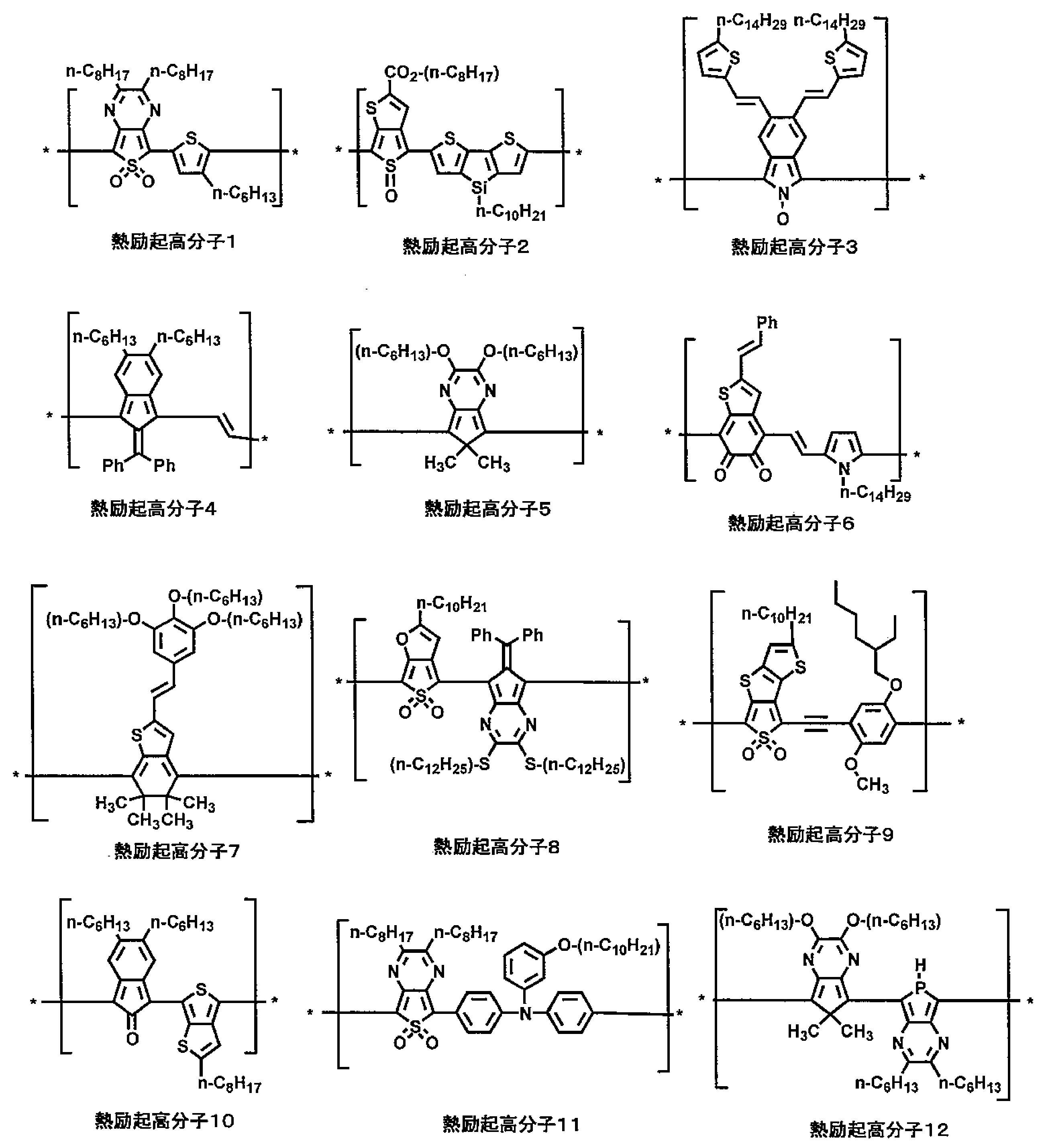
熱励起高分子101~107を以下に示す。
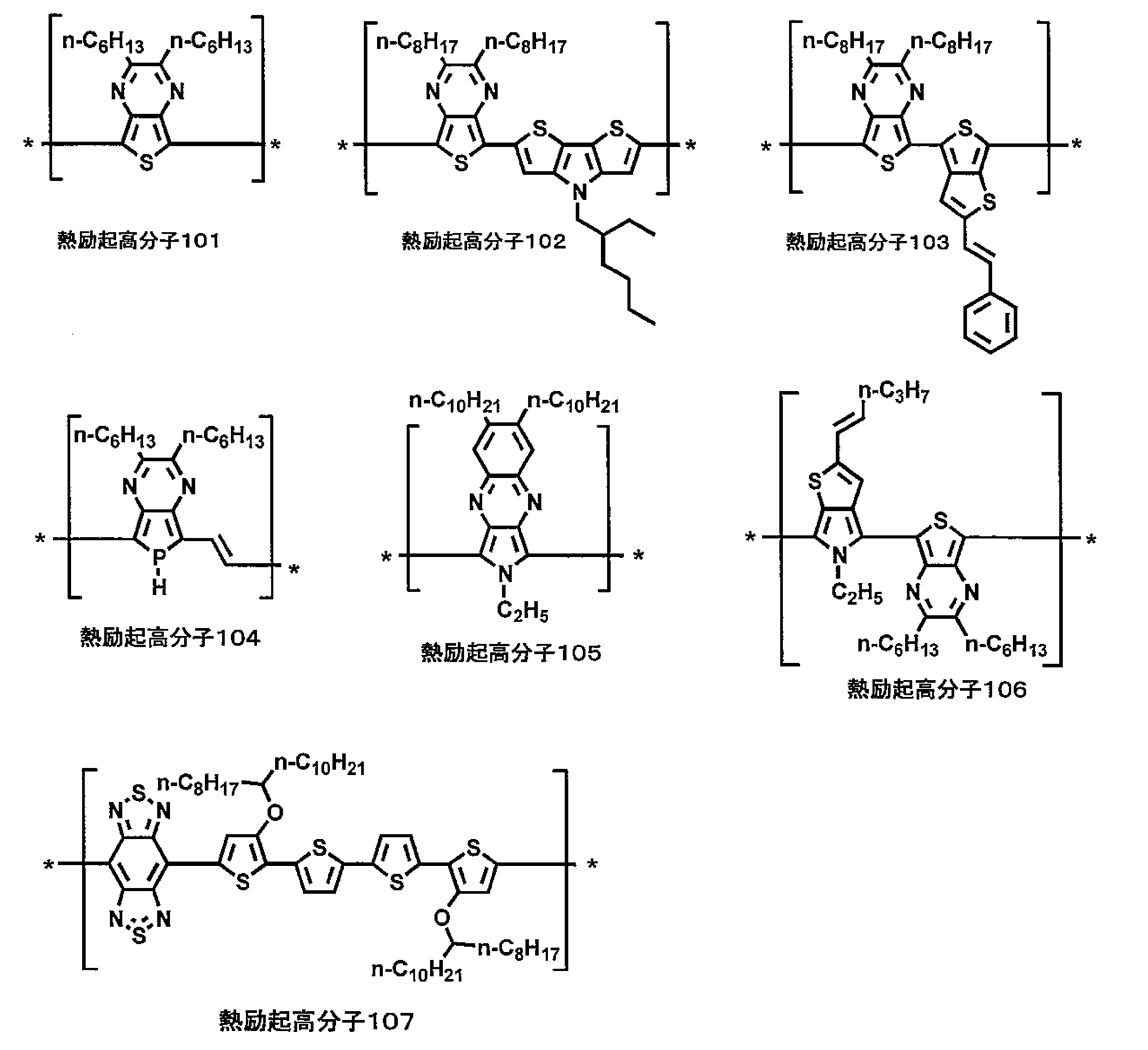
熱励起高分子1~12および101~107において、上記式(1)に示される繰り返し単位のA環の平均ユニット間距離L(計算値)、ならびに、各熱励起高分子の光学バンドギャップおよび重量平均分子量は下記の通りである。
熱励起高分子1:A環の平均ユニット間距離L(計算値)=1.36Å、光学バンドギャップ=0.3eV以下、重量平均分子量=13000
熱励起高分子2:A環の平均ユニット間距離L(計算値)=1.39Å、光学バンドギャップ=0.7eV、重量平均分子量=17000
熱励起高分子3:A環の平均ユニット間距離L(計算値)=1.40Å、光学バンドギャップ=0.7eV、重量平均分子量=27000
熱励起高分子4:A環の平均ユニット間距離L(計算値)=1.35Å、光学バンドギャップ=0.3eV以下、重量平均分子量=11000
熱励起高分子5:A環の平均ユニット間距離L(計算値)=1.36Å、光学バンドギャップ=0.3eV以下、重量平均分子量=16000
熱励起高分子6:A環の平均ユニット間距離L(計算値)=1.41Å、光学バンドギャップ=1.0eV、重量平均分子量=49000
熱励起高分子7:A環の平均ユニット間距離L(計算値)=1.38Å、光学バンドギャップ=0.6eV、重量平均分子量=27000
熱励起高分子8:A環の平均ユニット間距離L(計算値)=1.37Å、光学バンドギャップ=0.4eV、重量平均分子量=20000
熱励起高分子9:A環の平均ユニット間距離L(計算値)=1.40Å、光学バンドギャップ=0.9eV、重量平均分子量=61000
熱励起高分子10:A環の平均ユニット間距離L(計算値)=1.39Å、光学バンドギャップ=0.8eV、重量平均分子量=48000
熱励起高分子11:A環の平均ユニット間距離L(計算値)=1.42Å、光学バンドギャップ=1.1eV、重量平均分子量=39000
熱励起高分子12:A環の平均ユニット間距離L(計算値)=1.39Å、光学バンドギャップ=0.8eV、重量平均分子量=16000
熱励起高分子1:A環の平均ユニット間距離L(計算値)=1.36Å、光学バンドギャップ=0.3eV以下、重量平均分子量=13000
熱励起高分子2:A環の平均ユニット間距離L(計算値)=1.39Å、光学バンドギャップ=0.7eV、重量平均分子量=17000
熱励起高分子3:A環の平均ユニット間距離L(計算値)=1.40Å、光学バンドギャップ=0.7eV、重量平均分子量=27000
熱励起高分子4:A環の平均ユニット間距離L(計算値)=1.35Å、光学バンドギャップ=0.3eV以下、重量平均分子量=11000
熱励起高分子5:A環の平均ユニット間距離L(計算値)=1.36Å、光学バンドギャップ=0.3eV以下、重量平均分子量=16000
熱励起高分子6:A環の平均ユニット間距離L(計算値)=1.41Å、光学バンドギャップ=1.0eV、重量平均分子量=49000
熱励起高分子7:A環の平均ユニット間距離L(計算値)=1.38Å、光学バンドギャップ=0.6eV、重量平均分子量=27000
熱励起高分子8:A環の平均ユニット間距離L(計算値)=1.37Å、光学バンドギャップ=0.4eV、重量平均分子量=20000
熱励起高分子9:A環の平均ユニット間距離L(計算値)=1.40Å、光学バンドギャップ=0.9eV、重量平均分子量=61000
熱励起高分子10:A環の平均ユニット間距離L(計算値)=1.39Å、光学バンドギャップ=0.8eV、重量平均分子量=48000
熱励起高分子11:A環の平均ユニット間距離L(計算値)=1.42Å、光学バンドギャップ=1.1eV、重量平均分子量=39000
熱励起高分子12:A環の平均ユニット間距離L(計算値)=1.39Å、光学バンドギャップ=0.8eV、重量平均分子量=16000
熱励起高分子101:A環の平均ユニット間距離L(計算値)=1.42Å、光学バンドギャップ=1.1eV、重量平均分子量=22000
熱励起高分子102:A環の平均ユニット間距離L(計算値)=1.40Å、光学バンドギャップ=0.9eV、重量平均分子量=59000
熱励起高分子103:A環の平均ユニット間距離L(計算値)=1.41Å、光学バンドギャップ=1.0eV、重量平均分子量=35000
熱励起高分子104:A環の平均ユニット間距離L(計算値)=1.40Å、光学バンドギャップ=0.9eV、重量平均分子量=36000
熱励起高分子105:A環の平均ユニット間距離L(計算値)=1.42Å、光学バンドギャップ=1.1eV、重量平均分子量=14000
熱励起高分子106:A環の平均ユニット間距離L(計算値)=1.39Å、光学バンドギャップ=0.8eV、重量平均分子量=34000
熱励起高分子107:A環の平均ユニット間距離L(計算値)=1.38Å、光学バンドギャップ=0.6eV、重量平均分子量=32000
熱励起高分子102:A環の平均ユニット間距離L(計算値)=1.40Å、光学バンドギャップ=0.9eV、重量平均分子量=59000
熱励起高分子103:A環の平均ユニット間距離L(計算値)=1.41Å、光学バンドギャップ=1.0eV、重量平均分子量=35000
熱励起高分子104:A環の平均ユニット間距離L(計算値)=1.40Å、光学バンドギャップ=0.9eV、重量平均分子量=36000
熱励起高分子105:A環の平均ユニット間距離L(計算値)=1.42Å、光学バンドギャップ=1.1eV、重量平均分子量=14000
熱励起高分子106:A環の平均ユニット間距離L(計算値)=1.39Å、光学バンドギャップ=0.8eV、重量平均分子量=34000
熱励起高分子107:A環の平均ユニット間距離L(計算値)=1.38Å、光学バンドギャップ=0.6eV、重量平均分子量=32000
<A環の平均ユニット間距離Lの計算>
上述の計算法により算出した。すなわち、Gaussian計算法(使用プログラム名:Gaussian09(ガウシアン社製)、使用パラメータ:B3LYP/6-31G*)により、最適化された構造から原子間距離L1およびL2を算出し、上記式(I)による平均値を、A環の平均ユニット間距離L(計算値)とした。
上述の計算法により算出した。すなわち、Gaussian計算法(使用プログラム名:Gaussian09(ガウシアン社製)、使用パラメータ:B3LYP/6-31G*)により、最適化された構造から原子間距離L1およびL2を算出し、上記式(I)による平均値を、A環の平均ユニット間距離L(計算値)とした。
<光学バンドギャップの測定>
各熱励起高分子の光学バンドギャップは、下記の方法で算出した。
熱励起高分子を可溶性の有機溶媒に溶解させ、UVオゾン処理した石英基板(大きさ:15mm×15mm、厚み:1.1mm)上にスピンコート法で塗布した。塗布膜を真空条件下で1時間乾燥させて残存有機溶媒を留去した後、紫外可視近赤外(UV-Vis-NIR)分光光度計(株式会社島津製作所製、製品名:UV-3600)で吸収スペクトルを測定した。吸光度の極大値(λmax)に対し、吸光度が5%となる長波長側の吸収端の波長λ5(単位:nm)を求め、λ5を単位変換することにより光学バンドギャップ(単位:eV)を算出した。
各熱励起高分子の光学バンドギャップは、下記の方法で算出した。
熱励起高分子を可溶性の有機溶媒に溶解させ、UVオゾン処理した石英基板(大きさ:15mm×15mm、厚み:1.1mm)上にスピンコート法で塗布した。塗布膜を真空条件下で1時間乾燥させて残存有機溶媒を留去した後、紫外可視近赤外(UV-Vis-NIR)分光光度計(株式会社島津製作所製、製品名:UV-3600)で吸収スペクトルを測定した。吸光度の極大値(λmax)に対し、吸光度が5%となる長波長側の吸収端の波長λ5(単位:nm)を求め、λ5を単位変換することにより光学バンドギャップ(単位:eV)を算出した。
<重量平均分子量の測定>
熱励起高分子の重量平均分子量は、ゲル浸透クロマトグラフィー(GPC)によるポリスチレン換算値として求めた。
詳細には、熱励起高分子にo―ジクロロベンゼンを加えて145℃で溶解し、1.0μmの焼結フィルターでろ過して0.15w/v%の試料溶液を調製し、下記条件にて測定した。
装置:「Alliance GPC2000(Waters社製)」
カラム:「TSKgel GMH6-HT」-「TSKgel GMH6-HT」-「TSKgel GMH6-HTL」-「TSKgel GMH6-HTL」(いずれも7.5mmI.D.×30cm、東ソー社製)
カラム温度:140℃
検出器:示差屈折率計
移動相:o-ジクロロベンゼン
熱励起高分子の重量平均分子量は、ゲル浸透クロマトグラフィー(GPC)によるポリスチレン換算値として求めた。
詳細には、熱励起高分子にo―ジクロロベンゼンを加えて145℃で溶解し、1.0μmの焼結フィルターでろ過して0.15w/v%の試料溶液を調製し、下記条件にて測定した。
装置:「Alliance GPC2000(Waters社製)」
カラム:「TSKgel GMH6-HT」-「TSKgel GMH6-HT」-「TSKgel GMH6-HTL」-「TSKgel GMH6-HTL」(いずれも7.5mmI.D.×30cm、東ソー社製)
カラム温度:140℃
検出器:示差屈折率計
移動相:o-ジクロロベンゼン
[ナノ導電性材料]
単層CNT:「ASP-100F」(商品名、Hanwha Nanotech社製、分散物(CNT濃度60質量%)、長軸方向の平均長さ:約5~20μm、平均直径:約1.0~1.2nm)
グラファイト:「AGB-5」(商品名、伊藤黒鉛工業社製、一辺の平均長さ:5μm)
カーボンナノファイバー:「VGCF-X」(商品名、昭和電工社製、長軸方向の平均長さ:150nm)
グラフェン:「F-GF1205-AB」(商品名、SPI Supplies社製、一辺の平均長さ:10nm以上)
カーボンブラック:「ケッチェンブラックEC600JD」(商品名、ライオン社製、平均粒径:10nm以上)
カーボンナノ粒子:ナノダイヤモンドPL-D-G(商品名、PlasmaChem社製、平均粒径:10nm以上)
銀ナノワイヤー:特開2012-230881号公報に記載の調製法2に基づいて作製したもの(平均短軸長さ23nm、平均長軸長さ32μm)
ニッケルナノチューブ:特許第4374439号公報に記載の実施例1に基づく方法で作製したもの(直径100nm、長さ6μm)
金ナノ粒子:741973(製品番号、シグマアルドリッチ社製、粒径約30nm)
単層CNT:「ASP-100F」(商品名、Hanwha Nanotech社製、分散物(CNT濃度60質量%)、長軸方向の平均長さ:約5~20μm、平均直径:約1.0~1.2nm)
グラファイト:「AGB-5」(商品名、伊藤黒鉛工業社製、一辺の平均長さ:5μm)
カーボンナノファイバー:「VGCF-X」(商品名、昭和電工社製、長軸方向の平均長さ:150nm)
グラフェン:「F-GF1205-AB」(商品名、SPI Supplies社製、一辺の平均長さ:10nm以上)
カーボンブラック:「ケッチェンブラックEC600JD」(商品名、ライオン社製、平均粒径:10nm以上)
カーボンナノ粒子:ナノダイヤモンドPL-D-G(商品名、PlasmaChem社製、平均粒径:10nm以上)
銀ナノワイヤー:特開2012-230881号公報に記載の調製法2に基づいて作製したもの(平均短軸長さ23nm、平均長軸長さ32μm)
ニッケルナノチューブ:特許第4374439号公報に記載の実施例1に基づく方法で作製したもの(直径100nm、長さ6μm)
金ナノ粒子:741973(製品番号、シグマアルドリッチ社製、粒径約30nm)
<長軸方向の長さの測定>
ナノ導電性材料の長軸方向の長さは、下記の方法で算出した。
ナノ導電性材料の溶媒分散液(溶媒:水、オルト-ジクロロベンゼン、イソプロピルアルコール等)をガラス基板上に塗布した。塗布膜を真空下、100℃にて10時間乾燥させた後、塗布膜をガラス基板上から剥離させた。この剥離させた膜を、透過型電子顕微鏡(TEM)または走査型電子顕微鏡(SEM)を用いて観察し、ナノ導電性材料30個の長軸方向の長さを画像処理により測定し、これらの平均を算出した。
ナノ導電性材料の長軸方向の長さは、下記の方法で算出した。
ナノ導電性材料の溶媒分散液(溶媒:水、オルト-ジクロロベンゼン、イソプロピルアルコール等)をガラス基板上に塗布した。塗布膜を真空下、100℃にて10時間乾燥させた後、塗布膜をガラス基板上から剥離させた。この剥離させた膜を、透過型電子顕微鏡(TEM)または走査型電子顕微鏡(SEM)を用いて観察し、ナノ導電性材料30個の長軸方向の長さを画像処理により測定し、これらの平均を算出した。
[高分子バインダー]
1.共役高分子バインダー
共役高分子バインダーとして、下記バインダー1~6およびPEDOT:PPSを用いた。
1.共役高分子バインダー
共役高分子バインダーとして、下記バインダー1~6およびPEDOT:PPSを用いた。

共役高分子バインダー1~6およびPEDOT:PPSの上記繰り返し構造において、*は繰り返し構造の連結部位を表す。
共役高分子バインダー1~6の光学バンドギャップおよび重量平均分子量は下記の通りである。光学バンドギャップおよび重量平均分子量は上記熱励起高分子と同様にして測定した。
バインダー1:光学バンドギャップ=2.0eV、重量平均分子量=53000
バインダー2:光学バンドギャップ=2.0eV以上、重量平均分子量=20000
バインダー3:光学バンドギャップ=2.1eV、重量平均分子量=19000
バインダー4:光学バンドギャップ=2.0eV以上、重量平均分子量=41000
バインダー5:光学バンドギャップ=2.0eV以上、重量平均分子量=34000
バインダー6:光学バンドギャップ=2.0eV以上、重量平均分子量=26000
PEDOT:PSS:ポリ(3,4-エチレンジオキシチオフェン)ポリ(スチレンスルホネート)、エイチ・シー・スタルク社製、商品名「Baytron P」、PEDOT/PSS約1.3質量%の水分散物)、PEDOT/PSS(質量比)=1/2.5、光学バンドギャップ=約0eV
共役高分子バインダー1~6の光学バンドギャップおよび重量平均分子量は下記の通りである。光学バンドギャップおよび重量平均分子量は上記熱励起高分子と同様にして測定した。
バインダー1:光学バンドギャップ=2.0eV、重量平均分子量=53000
バインダー2:光学バンドギャップ=2.0eV以上、重量平均分子量=20000
バインダー3:光学バンドギャップ=2.1eV、重量平均分子量=19000
バインダー4:光学バンドギャップ=2.0eV以上、重量平均分子量=41000
バインダー5:光学バンドギャップ=2.0eV以上、重量平均分子量=34000
バインダー6:光学バンドギャップ=2.0eV以上、重量平均分子量=26000
PEDOT:PSS:ポリ(3,4-エチレンジオキシチオフェン)ポリ(スチレンスルホネート)、エイチ・シー・スタルク社製、商品名「Baytron P」、PEDOT/PSS約1.3質量%の水分散物)、PEDOT/PSS(質量比)=1/2.5、光学バンドギャップ=約0eV
<共役高分子バインダー2の合成例>
上記共役高分子バインダー2は、下記のように合成した。
9-(2-ethylhexyl)-9-(2-ethylpentyl)-2,7-bis(trimethylstannyl)-9H-fluorene(3.08g、4.38mmol)、methyl 3-(bis(4-bromophenyl)amino)benzoate(2.02g、4.38mmol)、テトラキストリフェニルホスフィンパラジウム(253mg、0.219mmol)を200mLのフラスコ内に導入し、容器内を窒素置換した。この容器内に、溶媒としてトルエン(35mL)およびN,N-ジメチルホルムアミド(9mL)を、シリンジを用いて添加した後、120℃のオイルバスにて窒素雰囲気下、24時間加熱撹拌して反応させた。反応液を室温まで冷却した後、セライト濾過して不溶成分を除去した。得られた濾液をメタノール中に少量ずつ滴下し、固形物を析出させた後、固形物を濾過により分取した。この固形物を、ソックスレー抽出器を用いてアセトン溶媒により10時間加熱洗浄し、不純物を除去した。最後にこの固形物を真空下にて10時間乾燥させることにより、目的とする共役高分子バインダー2を得た(収量2.21g、収率73%)。
上記共役高分子バインダー2は、下記のように合成した。
9-(2-ethylhexyl)-9-(2-ethylpentyl)-2,7-bis(trimethylstannyl)-9H-fluorene(3.08g、4.38mmol)、methyl 3-(bis(4-bromophenyl)amino)benzoate(2.02g、4.38mmol)、テトラキストリフェニルホスフィンパラジウム(253mg、0.219mmol)を200mLのフラスコ内に導入し、容器内を窒素置換した。この容器内に、溶媒としてトルエン(35mL)およびN,N-ジメチルホルムアミド(9mL)を、シリンジを用いて添加した後、120℃のオイルバスにて窒素雰囲気下、24時間加熱撹拌して反応させた。反応液を室温まで冷却した後、セライト濾過して不溶成分を除去した。得られた濾液をメタノール中に少量ずつ滴下し、固形物を析出させた後、固形物を濾過により分取した。この固形物を、ソックスレー抽出器を用いてアセトン溶媒により10時間加熱洗浄し、不純物を除去した。最後にこの固形物を真空下にて10時間乾燥させることにより、目的とする共役高分子バインダー2を得た(収量2.21g、収率73%)。
2.非共役高分子バインダー
非共役高分子バインダーとして、下記のポリマーを用いた。
ポリスチレン:430102(製品番号、アルドリッチ社製、重量平均分子量=192000)
ポリメチルメタクリレート:和光純薬工業社製
ポリ酢酸ビニル:和光純薬工業社製
ポリ乳酸:PLA-0015(商品名、和光純薬工業社製)
ポリビニルピロリドン:和光純薬工業社製
ポリイミド:ソルピー6,6-PI(商品名、ソルピー工業社製)
ポリカーボネート:ユピゼータPCZ-300(商品名、三菱ガス化学社製)
非共役高分子バインダーとして、下記のポリマーを用いた。
ポリスチレン:430102(製品番号、アルドリッチ社製、重量平均分子量=192000)
ポリメチルメタクリレート:和光純薬工業社製
ポリ酢酸ビニル:和光純薬工業社製
ポリ乳酸:PLA-0015(商品名、和光純薬工業社製)
ポリビニルピロリドン:和光純薬工業社製
ポリイミド:ソルピー6,6-PI(商品名、ソルピー工業社製)
ポリカーボネート:ユピゼータPCZ-300(商品名、三菱ガス化学社製)
[ドーパント]
ドーパントとして、下記の化合物1~4を用いた。
ドーパントとして、下記の化合物1~4を用いた。
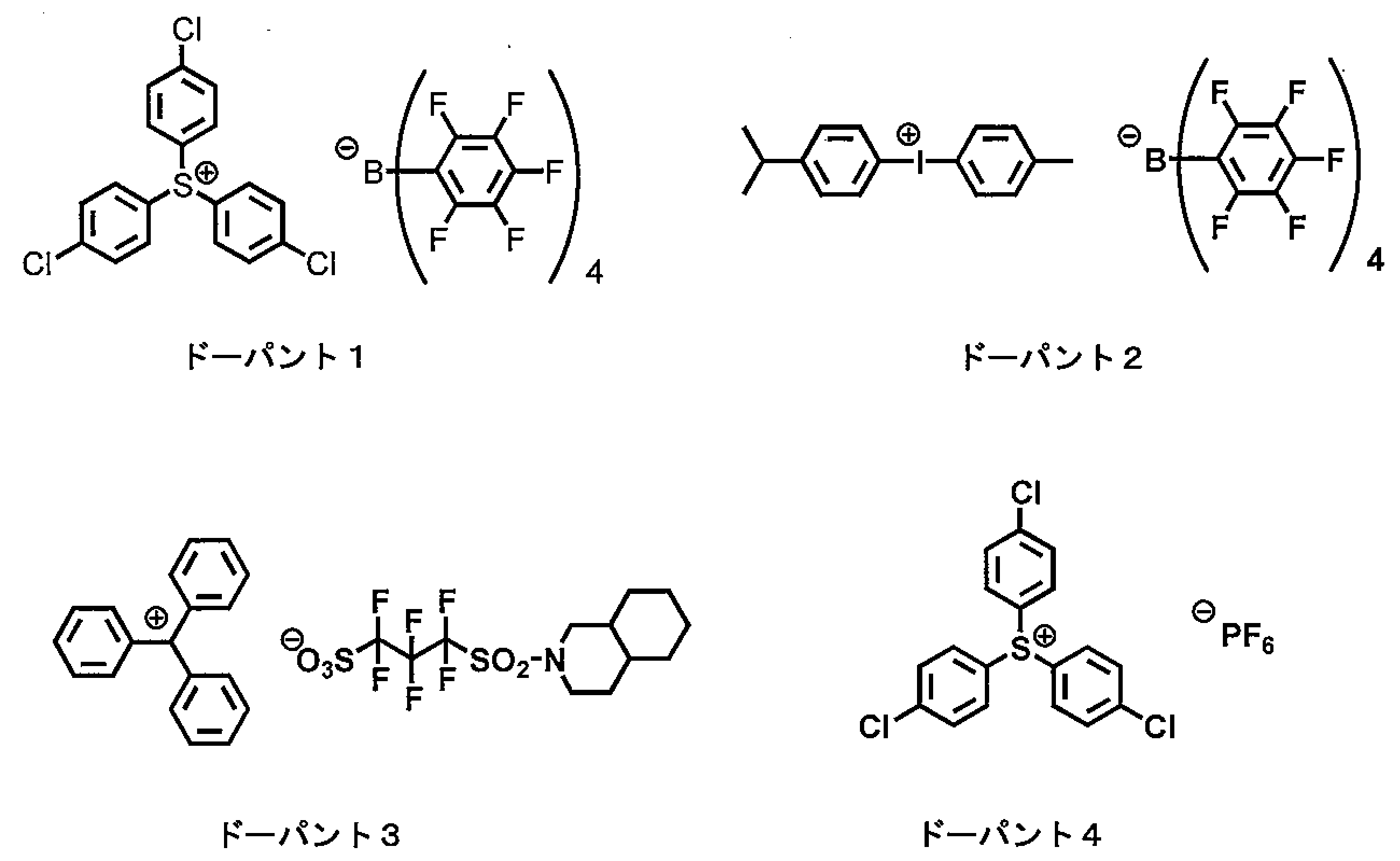
実施例1
熱励起高分子1 6mg、および、上記単層CNT 4mg(CNT濃度換算)を、オルトジクロロベンゼン4.0mL中に添加し、温度制御機能付き超音波水浴(エスエヌディ社製、US-10KS)にて35℃で40分間分散させて熱電変換材料としての分散液を調製した。この分散液を、第一の電極13として金(厚み20nm、幅:5mm)を片側表面に有するガラス基材12(厚み:0.8mm)の電極13表面にスクリーン印刷法で塗布し、80℃にて45分間加熱して溶媒を除去した。その後、室温真空下にて10時間乾燥させることにより膜厚2.2μm、大きさ8mm×8mmの熱電変換層14を形成した。その後、熱電変換層14の上部に、第2の電極15として金を蒸着したガラス基材16(電極15の厚み:20nm、電極15の幅:5mm、ガラス基材16の厚み:0.8mm)を、第2の電極15が熱電変換層14に対向するように、80℃にて貼り合わせて、図1に示される熱電変換素子1である本発明の熱電変換素子101を作製した。
熱励起高分子1 6mg、および、上記単層CNT 4mg(CNT濃度換算)を、オルトジクロロベンゼン4.0mL中に添加し、温度制御機能付き超音波水浴(エスエヌディ社製、US-10KS)にて35℃で40分間分散させて熱電変換材料としての分散液を調製した。この分散液を、第一の電極13として金(厚み20nm、幅:5mm)を片側表面に有するガラス基材12(厚み:0.8mm)の電極13表面にスクリーン印刷法で塗布し、80℃にて45分間加熱して溶媒を除去した。その後、室温真空下にて10時間乾燥させることにより膜厚2.2μm、大きさ8mm×8mmの熱電変換層14を形成した。その後、熱電変換層14の上部に、第2の電極15として金を蒸着したガラス基材16(電極15の厚み:20nm、電極15の幅:5mm、ガラス基材16の厚み:0.8mm)を、第2の電極15が熱電変換層14に対向するように、80℃にて貼り合わせて、図1に示される熱電変換素子1である本発明の熱電変換素子101を作製した。
熱励起高分子、ナノ導電性材料および電極材料を下記表1に示すように変更した以外は熱電変換素子101と同様にして、本発明の熱電変換素子102~119および比較の熱電変換素子c101~c105を作製した。
[ナノ導電性材料の分散性評価]
上記で得られた超音波分散後の分散液におけるナノ導電性材料(単層CNT)の分散性を次のように評価した。結果を表1に示す。
マイクロトラックMT3300型レーザー回折散乱式粒度分布測定装置(日機装社製)を用い、0.1~2000μmの範囲を測定し、50%累積頻度となるときの体積平均粒径(D50)を算出した。この体積平均粒径の値から下記のように、単層CNTの分散性を下記A~Eの5ランクに分類した。実用上、A~Cの基準を満たすことが好ましい。
A:体積平均粒径が150nm未満
B:体積平均粒径が150nm以上300nm未満
C:体積平均粒径が300nm以上600nm未満
D:体積平均粒径が600nm以上だが沈殿物や凝集物が目視で確認できない。
E:沈殿物や凝集物が目視で確認できる。
上記で得られた超音波分散後の分散液におけるナノ導電性材料(単層CNT)の分散性を次のように評価した。結果を表1に示す。
マイクロトラックMT3300型レーザー回折散乱式粒度分布測定装置(日機装社製)を用い、0.1~2000μmの範囲を測定し、50%累積頻度となるときの体積平均粒径(D50)を算出した。この体積平均粒径の値から下記のように、単層CNTの分散性を下記A~Eの5ランクに分類した。実用上、A~Cの基準を満たすことが好ましい。
A:体積平均粒径が150nm未満
B:体積平均粒径が150nm以上300nm未満
C:体積平均粒径が300nm以上600nm未満
D:体積平均粒径が600nm以上だが沈殿物や凝集物が目視で確認できない。
E:沈殿物や凝集物が目視で確認できる。
[熱電特性値(熱起電力S)の測定]
各熱電変換素子について、下記の方法により、熱電特性値(熱起電力S)を評価した。結果を表1に示す。
各熱電変換素子について、下記の方法により、熱電特性値(熱起電力S)を評価した。結果を表1に示す。
各熱電変換素子の第1の電極13を一定温度に保ったホットプレート上に設置し、第2の電極15上に温度制御用のペルチェ素子を設置した。ホットプレートの温度を一定(100℃)に保ちつつ、ペルチェ素子の温度を低下させることにより両電極間に温度差(0Kを超え4K以下の範囲)を付与した。この時、両電極間に発生した熱起電力(μV)を両電極間に生じた特定の温度差(K)で除することにより、単位温度差当たりの熱起電力S(μV/K)を算出し、この値を熱電変換素子の熱電特性値とした。算出した熱電特性値を、比較の熱電変換素子c101の算出値に対する相対値として、表1に示す。

表1から明らかなように、長軸方向の平均長さが少なくとも5nmであるナノ導電性材料と本発明の熱励起高分子化合物を含有する本発明の熱電変換素子101~119は、いずれも、熱起電力Sが高いことに加えて、ナノ導電性材料の分散性に優れていた。
これに対し、ナノ導電性材料および本発明の熱励起高分子化合物の少なくとも一方を含有しない比較の熱電変換素子c101~c105は、熱起電力が低く、またはナノ導電性材料の分散性が本発明の合格基準を満たしていなかった。
これに対し、ナノ導電性材料および本発明の熱励起高分子化合物の少なくとも一方を含有しない比較の熱電変換素子c101~c105は、熱起電力が低く、またはナノ導電性材料の分散性が本発明の合格基準を満たしていなかった。
実施例2
熱励起高分子1 4mg、上記単層CNT 2mg(CNT濃度換算)、高分子バインダーとしてポリスチレン 4mgを、オルトジクロロベンゼン4.0mL中に添加し、超音波水浴にて40分間分散させた。この分散液を、第一の電極13として金(厚み20nm、幅:5mm)を片側表面に有するガラス基材12(厚み:0.8mm)の電極13表面にスクリーン印刷法で塗布し、80℃にて45分間加熱して溶媒を除去した。その後、室温真空下にて10時間乾燥させることにより膜厚2.1μm、大きさ8mm×8mmの熱電変換層14を形成した。その後、熱電変換層14の上部に、第2の電極15として金を蒸着したガラス基材16(電極15の厚み:20nm、電極15の幅:5mm、ガラス基材16の厚み:0.8mm)を、第2の電極15が熱電変換層14に対向するように、80℃にて貼り合わせて、図1に示される熱電変換素子1である本発明の熱電変換素子201を作製した。
熱励起高分子1 4mg、上記単層CNT 2mg(CNT濃度換算)、高分子バインダーとしてポリスチレン 4mgを、オルトジクロロベンゼン4.0mL中に添加し、超音波水浴にて40分間分散させた。この分散液を、第一の電極13として金(厚み20nm、幅:5mm)を片側表面に有するガラス基材12(厚み:0.8mm)の電極13表面にスクリーン印刷法で塗布し、80℃にて45分間加熱して溶媒を除去した。その後、室温真空下にて10時間乾燥させることにより膜厚2.1μm、大きさ8mm×8mmの熱電変換層14を形成した。その後、熱電変換層14の上部に、第2の電極15として金を蒸着したガラス基材16(電極15の厚み:20nm、電極15の幅:5mm、ガラス基材16の厚み:0.8mm)を、第2の電極15が熱電変換層14に対向するように、80℃にて貼り合わせて、図1に示される熱電変換素子1である本発明の熱電変換素子201を作製した。
熱励起高分子、高分子バインダーおよびナノ導電性材料を下記表2に示すように変更した以外は熱電変換素子201と同様にして、本発明の熱電変換素子202~214および比較の熱電変換素子c201を作製した。
なお、熱電変換素子212において、バインダー2とポリカーボネートとの使用割合(質量比)は50:50であった。
なお、熱電変換素子212において、バインダー2とポリカーボネートとの使用割合(質量比)は50:50であった。
実施例1と同様にして、ナノ導電性材料の分散性を評価し、熱電特性値(熱起電力S)を測定した。表2に示した熱電特性値(熱起電力S)は、実施例1で作製した比較の熱電変換素子c101の算出値に対する相対値である。結果を表2に示す。

表2から明らかなように、長軸方向の平均長さが少なくとも5nmであるナノ導電性材料と本発明の熱励起高分子化合物を含有する本発明の熱電変換素子201~114は、いずれも、熱起電力が高いことに加えて、ナノ導電性材料の分散性に優れていた。
これに対し、本発明の熱励起高分子化合物を含有しない比較の熱電変換素子c201は、高分子バインダーを含有していても、熱起電力が低く、またナノ導電性材料の分散性も本発明の合格基準を満たしていなかった。
これに対し、本発明の熱励起高分子化合物を含有しない比較の熱電変換素子c201は、高分子バインダーを含有していても、熱起電力が低く、またナノ導電性材料の分散性も本発明の合格基準を満たしていなかった。
実施例3
熱励起高分子1 4mg、上記単層CNT 4mg(CNT濃度換算)、ドーパント1 2mgを、オルトジクロロベンゼン4.0mL中に添加し、超音波水浴にて40分間分散させた。この分散液を、第一の電極13として金(厚み20nm、幅:5mm)を片側表面に有するガラス基材12(厚み:0.8mm)の電極13表面にスクリーン印刷法で塗布し、80℃にて45分間加熱して溶媒を除去した。その後、室温真空下にて10時間乾燥させることにより膜厚2.2μm、大きさ8mm×8mmの熱電変換層14を形成した。この熱電変換層14を、乾燥後に、紫外線照射機(アイグラフィックス株式会社製、ECS-401GX)により紫外線を照射して(光量:1.06J/cm2)、ドーピングした。その後、熱電変換層14の上部に、第2の電極15として金を蒸着したガラス基材16(電極15の厚み:20nm、電極15の幅:5mm、ガラス基材16の厚み:0.8mm)を、第2の電極15が熱電変換層14に対向するように、80℃にて貼り合わせて、図1に示される熱電変換素子1である本発明の熱電変換素子301を作製した。
熱励起高分子1 4mg、上記単層CNT 4mg(CNT濃度換算)、ドーパント1 2mgを、オルトジクロロベンゼン4.0mL中に添加し、超音波水浴にて40分間分散させた。この分散液を、第一の電極13として金(厚み20nm、幅:5mm)を片側表面に有するガラス基材12(厚み:0.8mm)の電極13表面にスクリーン印刷法で塗布し、80℃にて45分間加熱して溶媒を除去した。その後、室温真空下にて10時間乾燥させることにより膜厚2.2μm、大きさ8mm×8mmの熱電変換層14を形成した。この熱電変換層14を、乾燥後に、紫外線照射機(アイグラフィックス株式会社製、ECS-401GX)により紫外線を照射して(光量:1.06J/cm2)、ドーピングした。その後、熱電変換層14の上部に、第2の電極15として金を蒸着したガラス基材16(電極15の厚み:20nm、電極15の幅:5mm、ガラス基材16の厚み:0.8mm)を、第2の電極15が熱電変換層14に対向するように、80℃にて貼り合わせて、図1に示される熱電変換素子1である本発明の熱電変換素子301を作製した。
熱励起高分子およびドーパントを下記表3に示すように変更した以外は熱電変換素子301と同様にして、本発明の熱電変換素子302~308を作製した。なお、熱電変換素子306では紫外線照射によるドーピング処理は行わなかった。
なお、熱電変換素子302および304において、熱励起高分子、高分子バインダー、単層CNTおよびドーパントとの使用割合(質量比)は、いずれも、40:20:30:10であった。
なお、熱電変換素子302および304において、熱励起高分子、高分子バインダー、単層CNTおよびドーパントとの使用割合(質量比)は、いずれも、40:20:30:10であった。
実施例1と同様にして、単層CNTの分散性を評価し、熱電特性値(熱起電力S)を測定した。表3に示した熱電特性値(熱起電力S)は、実施例1で作製した比較の熱電変換素子c101の算出値に対する相対値である。結果を表3に示す。

表3から明らかなように、長軸方向の平均長さが少なくとも5nmである粒子からなるナノ導電性材料と本発明の熱励起高分子化合物を含有する本発明の熱電変換素子301~308は、いずれも、熱起電力が高いことに加えて、ナノ導電性材料の分散性に優れていた。
本発明をその実施態様とともに説明したが、我々は特に指定しない限り我々の発明を説明のどの細部においても限定しようとするものではなく、添付の請求の範囲に示した発明の精神と範囲に反することなく幅広く解釈されるべきであると考える。
本願は、2013年9月4日に日本国で特許出願された特願2013-183099に基づく優先権を主張するものであり、これはここに参照してその内容を本明細書の記載の一部として取り込む。
1、2 熱電変換素子
11、17 金属板
12、22 第1の基材
13、23 第1の電極
14、24 熱電変換層
15、25 第2の電極
16、26 第2の基材
11、17 金属板
12、22 第1の基材
13、23 第1の電極
14、24 熱電変換層
15、25 第2の電極
16、26 第2の基材
Claims (20)
- 基材上に、第1の電極、熱電変換層および第2の電極を有する熱電変換素子であって、
該熱電変換層が、長軸方向の平均長さが少なくとも5nmであるナノ導電性材料、および、下記式(1)で表される繰り返し単位を有する熱励起高分子化合物を含有する熱電変換素子。

- 前記熱励起高分子化合物が、下記式(2)で表される繰り返し単位を有する請求項1に記載の熱電変換素子。

- A環の環構造が、下記式(3)~(8)のいずれかの式で表される環構造である請求項1または2に記載の熱電変換素子。
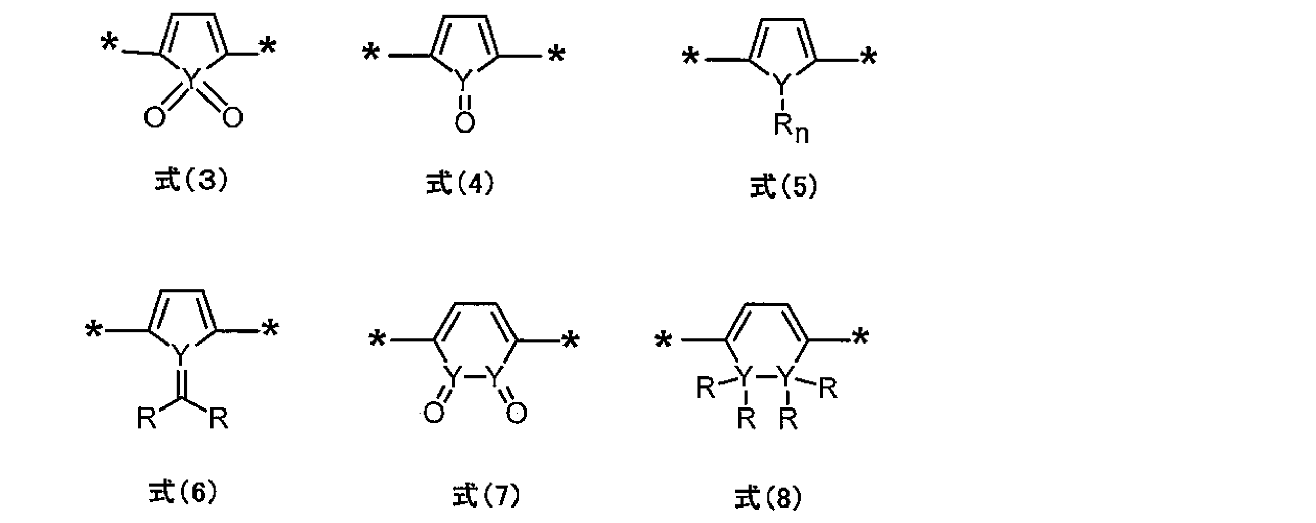
- 前記B環が、ベンゼン環または5員もしくは6員の芳香族ヘテロ環である請求項2または3に記載の熱電変換素子。
- 前記熱励起高分子化合物が、エテニレン基、エチニレン基、アリーレン基、ヘテロアリーレン基からなる群より選択される少なくとも1種の繰り返し単位を有する請求項1~4のいずれか1項に記載の熱電変換素子。
- 前記熱電変換層が、共役高分子バインダーおよび非共役高分子バインダーから選ばれる少なくとも1種の高分子バインダーを含有する請求項1~5のいずれか1項に記載の熱電変換素子。
- 前記ナノ導電性材料が、ナノ炭素材料またはナノ金属材料である請求項1~6のいずれか1項に記載の熱電変換素子。
- 前記ナノ導電性材料が、カーボンナノチューブ、カーボンナノファイバー、グラファイト、グラフェン、カーボンナノ粒子および金属ナノワイヤーからなる群より選択される少なくとも1つである請求項1~7のいずれか1項に記載の熱電変換素子。
- 前記ナノ導電性材料が、カーボンナノチューブである請求項1~8のいずれか1項に記載の熱電変換素子。
- 前記熱電変換層が、ドーパントを含有する請求項1~9のいずれか1項に記載の熱電変換素子。
- 前記基材が、フレキシビリティーを有する請求項1~10のいずれか1項に記載の熱電変換素子。
- 前記第1の電極および第2の電極が、各々独立に、アルミニウム、金、銀または銅で形成されてなる請求項1~11のいずれか1項に記載に記載の熱電変換素子。
- 請求項1~12のいずれか1項に記載の熱電変換素子を用いた熱電発電用物品。
- 請求項1~12のいずれか1項に記載の熱電変換素子を用いたセンサー用電源。
- 長軸方向の平均長さが少なくとも5nmであるナノ導電性材料、および、下記式(1)で表される繰り返し単位を有する熱励起高分子化合物を含有する、熱電変換素子の熱電変換層を形成するための熱電変換材料。

- 前記熱励起高分子化合物が、下記式(2)で表される繰り返し単位を有する請求項15に記載の熱電変換材料。

- 前記B環が、ベンゼン環または5員もしくは6員の芳香族ヘテロ環である請求項16に記載の熱電変換材料。
- 共役高分子バインダーおよび非共役高分子バインダーから選ばれる少なくとも1種の高分子バインダーを含有する請求項15~17のいずれか1項に記載の熱電変換材料。
- 有機溶媒を含む請求項15~18のいずれか1項に記載の熱電変換材料。
- 前記ナノ導電性材料を前記有機溶媒中に分散してなる請求項19に記載の熱電変換材料。
Priority Applications (1)
| Application Number | Priority Date | Filing Date | Title |
|---|---|---|---|
| US15/059,937 US20160260882A1 (en) | 2013-09-04 | 2016-03-03 | Thermoelectric conversion material, thermoelectric conversion element, article for thermoelectric power generation, and power source for sensor |
Applications Claiming Priority (2)
| Application Number | Priority Date | Filing Date | Title |
|---|---|---|---|
| JP2013-183099 | 2013-09-04 | ||
| JP2013183099A JP6047468B2 (ja) | 2013-09-04 | 2013-09-04 | 熱電変換材料、熱電変換素子、熱電発電用物品およびセンサー用電源 |
Related Child Applications (1)
| Application Number | Title | Priority Date | Filing Date |
|---|---|---|---|
| US15/059,937 Continuation US20160260882A1 (en) | 2013-09-04 | 2016-03-03 | Thermoelectric conversion material, thermoelectric conversion element, article for thermoelectric power generation, and power source for sensor |
Publications (1)
| Publication Number | Publication Date |
|---|---|
| WO2015033832A1 true WO2015033832A1 (ja) | 2015-03-12 |
Family
ID=52628308
Family Applications (1)
| Application Number | Title | Priority Date | Filing Date |
|---|---|---|---|
| PCT/JP2014/072419 Ceased WO2015033832A1 (ja) | 2013-09-04 | 2014-08-27 | 熱電変換材料、熱電変換素子、熱電発電用物品およびセンサー用電源 |
Country Status (3)
| Country | Link |
|---|---|
| US (1) | US20160260882A1 (ja) |
| JP (1) | JP6047468B2 (ja) |
| WO (1) | WO2015033832A1 (ja) |
Cited By (3)
| Publication number | Priority date | Publication date | Assignee | Title |
|---|---|---|---|---|
| CN110600613A (zh) * | 2019-09-18 | 2019-12-20 | 中国科学院大学 | 一种聚合物光电探测器及其制备方法 |
| CN110655640A (zh) * | 2019-08-02 | 2020-01-07 | 中国科学院大学 | 一种室温柔性日盲型短波红外聚合物光电探测器及其制备方法 |
| CN115971010A (zh) * | 2022-12-29 | 2023-04-18 | 西北工业大学太仓长三角研究院 | 一种制备纳米复合材料压阻式应变传感器的方法 |
Families Citing this family (11)
| Publication number | Priority date | Publication date | Assignee | Title |
|---|---|---|---|---|
| CN106165132A (zh) * | 2014-02-28 | 2016-11-23 | 国立大学法人奈良先端科学技术大学院大学 | 热电转换材料和热电转换元件 |
| JP6292719B2 (ja) | 2015-03-13 | 2018-03-14 | オムロンオートモーティブエレクトロニクス株式会社 | 車両無線通信システム、車両制御装置、携帯機 |
| JP6629643B2 (ja) * | 2016-03-08 | 2020-01-15 | 公立大学法人山陽小野田市立山口東京理科大学 | 熱電変換素子の製造方法及び熱電変換素子 |
| KR101808827B1 (ko) * | 2016-06-16 | 2017-12-14 | 한국화학연구원 | 전기전도성이 우수한 열전재료 조성물 및 이의 제조방법 |
| WO2018147126A1 (ja) * | 2017-02-10 | 2018-08-16 | 国立大学法人 奈良先端科学技術大学院大学 | n型導電材料およびその製造方法 |
| JP6936859B2 (ja) * | 2017-07-28 | 2021-09-22 | 富士フイルム株式会社 | センサ |
| JP2019106410A (ja) * | 2017-12-08 | 2019-06-27 | 株式会社東芝 | 熱電変換素子、及び熱電変換素子の製造方法 |
| JP7041662B2 (ja) * | 2018-12-20 | 2022-03-24 | コーロン インダストリーズ インク | ポリアミック酸、ポリイミド樹脂及びポリイミドフィルム |
| KR102764008B1 (ko) * | 2020-01-30 | 2025-02-05 | 삼성전자주식회사 | 적외선 흡수재, 적외선 흡수/차단 필름, 광전 소자, 유기 센서 및 전자 장치 |
| JP2021028982A (ja) * | 2020-11-04 | 2021-02-25 | 東洋インキScホールディングス株式会社 | 導電性組成物、熱電変換材料、および熱電変換素子 |
| US20250019243A1 (en) * | 2021-11-29 | 2025-01-16 | Duke University | Metallic single-walled carbon nanotube hybrid assemblies and superstructures |
Citations (4)
| Publication number | Priority date | Publication date | Assignee | Title |
|---|---|---|---|---|
| JP2012251132A (ja) * | 2011-03-28 | 2012-12-20 | Fujifilm Corp | 導電性組成物、当該組成物を用いた導電性膜及びその製造方法 |
| US20130084464A1 (en) * | 2010-05-24 | 2013-04-04 | The Regents Of The University Of California | Inorganic Nanostructure-Organic Polymer Heterostructures Useful for Thermoelectric Devices |
| JP2013084947A (ja) * | 2011-09-28 | 2013-05-09 | Fujifilm Corp | 熱電変換材料及び熱電変換素子 |
| JP2013098299A (ja) * | 2011-10-31 | 2013-05-20 | Fujifilm Corp | 熱電変換材料及び熱電変換素子 |
-
2013
- 2013-09-04 JP JP2013183099A patent/JP6047468B2/ja not_active Expired - Fee Related
-
2014
- 2014-08-27 WO PCT/JP2014/072419 patent/WO2015033832A1/ja not_active Ceased
-
2016
- 2016-03-03 US US15/059,937 patent/US20160260882A1/en not_active Abandoned
Patent Citations (4)
| Publication number | Priority date | Publication date | Assignee | Title |
|---|---|---|---|---|
| US20130084464A1 (en) * | 2010-05-24 | 2013-04-04 | The Regents Of The University Of California | Inorganic Nanostructure-Organic Polymer Heterostructures Useful for Thermoelectric Devices |
| JP2012251132A (ja) * | 2011-03-28 | 2012-12-20 | Fujifilm Corp | 導電性組成物、当該組成物を用いた導電性膜及びその製造方法 |
| JP2013084947A (ja) * | 2011-09-28 | 2013-05-09 | Fujifilm Corp | 熱電変換材料及び熱電変換素子 |
| JP2013098299A (ja) * | 2011-10-31 | 2013-05-20 | Fujifilm Corp | 熱電変換材料及び熱電変換素子 |
Non-Patent Citations (1)
| Title |
|---|
| LI WEN ET AL.: "Poly(2,3-dihexylthieno[3,4-b] pyrazine) via GRIM Polymerization: Simple Preparation of a Solution Processable, Low- Band-Gap Conjugated Polymer", MACROMOLECULES, vol. 41, no. 13, 2008, pages 4576 - 4578 * |
Cited By (5)
| Publication number | Priority date | Publication date | Assignee | Title |
|---|---|---|---|---|
| CN110655640A (zh) * | 2019-08-02 | 2020-01-07 | 中国科学院大学 | 一种室温柔性日盲型短波红外聚合物光电探测器及其制备方法 |
| CN110655640B (zh) * | 2019-08-02 | 2022-01-18 | 中国科学院大学 | 一种室温柔性日盲型短波红外聚合物光电探测器及其制备方法 |
| CN110600613A (zh) * | 2019-09-18 | 2019-12-20 | 中国科学院大学 | 一种聚合物光电探测器及其制备方法 |
| CN110600613B (zh) * | 2019-09-18 | 2022-04-26 | 中国科学院大学 | 一种聚合物光电探测器及其制备方法 |
| CN115971010A (zh) * | 2022-12-29 | 2023-04-18 | 西北工业大学太仓长三角研究院 | 一种制备纳米复合材料压阻式应变传感器的方法 |
Also Published As
| Publication number | Publication date |
|---|---|
| JP2015050420A (ja) | 2015-03-16 |
| JP6047468B2 (ja) | 2016-12-21 |
| US20160260882A1 (en) | 2016-09-08 |
Similar Documents
| Publication | Publication Date | Title |
|---|---|---|
| JP6047468B2 (ja) | 熱電変換材料、熱電変換素子、熱電発電用物品およびセンサー用電源 | |
| JP5976604B2 (ja) | 熱電変換材料、熱電変換素子、熱電発電用物品及びセンサー用電源 | |
| JP5670980B2 (ja) | 熱電変換材料及び熱電変換素子 | |
| JP5960178B2 (ja) | 熱電変換素子の製造方法および熱電変換層用分散物の製造方法 | |
| JP5951539B2 (ja) | 熱電変換材料、熱電変換素子ならびにこれを用いた熱電発電用物品およびセンサー用電源 | |
| JP5789580B2 (ja) | 熱電変換材料及び熱電変換素子 | |
| JP2013098299A (ja) | 熱電変換材料及び熱電変換素子 | |
| CN104919609B (zh) | 热电转换材料、热电转换元件以及使用其的热电发电用物品和传感器用电源 | |
| JP2013016293A (ja) | 透明導電膜とその製造方法、並びに有機電子素子、有機発光素子及び有機発電素子 | |
| WO2014119468A1 (ja) | 熱電変換材料、熱電変換素子並びにこれを用いた熱電発電用物品及びセンサー用電源 | |
| CN104919608B (zh) | 热电转换材料、热电转换元件以及使用其的热电发电用物品和传感器用电源 | |
| WO2015050112A1 (ja) | フレキシブル有機熱電変換素子及びその製造方法、並びに、熱電発電用物品及びセンサー用電源 | |
| JP5931763B2 (ja) | 熱電変換材料、熱電変換素子並びにこれを用いた熱電発電用物品及びセンサー用電源 | |
| JP2015189804A (ja) | 導電性組成物、導電膜及び有機半導体デバイス | |
| WO2016052514A1 (ja) | 熱電変換素子、導電膜、有機半導体デバイス、及び導電性組成物 |
Legal Events
| Date | Code | Title | Description |
|---|---|---|---|
| 121 | Ep: the epo has been informed by wipo that ep was designated in this application |
Ref document number: 14841982 Country of ref document: EP Kind code of ref document: A1 |
|
| NENP | Non-entry into the national phase |
Ref country code: DE |
|
| 122 | Ep: pct application non-entry in european phase |
Ref document number: 14841982 Country of ref document: EP Kind code of ref document: A1 |