WO2015029358A1 - 放射線検出装置およびその製造方法 - Google Patents
放射線検出装置およびその製造方法 Download PDFInfo
- Publication number
- WO2015029358A1 WO2015029358A1 PCT/JP2014/004184 JP2014004184W WO2015029358A1 WO 2015029358 A1 WO2015029358 A1 WO 2015029358A1 JP 2014004184 W JP2014004184 W JP 2014004184W WO 2015029358 A1 WO2015029358 A1 WO 2015029358A1
- Authority
- WO
- WIPO (PCT)
- Prior art keywords
- support substrate
- bonding layer
- radiation detection
- substrate
- detection apparatus
- Prior art date
- Legal status (The legal status is an assumption and is not a legal conclusion. Google has not performed a legal analysis and makes no representation as to the accuracy of the status listed.)
- Ceased
Links
Images






Classifications
-
- G—PHYSICS
- G01—MEASURING; TESTING
- G01T—MEASUREMENT OF NUCLEAR OR X-RADIATION
- G01T1/00—Measuring X-radiation, gamma radiation, corpuscular radiation, or cosmic radiation
- G01T1/16—Measuring radiation intensity
- G01T1/20—Measuring radiation intensity with scintillation detectors
- G01T1/2006—Measuring radiation intensity with scintillation detectors using a combination of a scintillator and photodetector which measures the means radiation intensity
Definitions
- the present invention relates to a radiation detection apparatus and a manufacturing method thereof.
- a radiation detection device in which a scintillator layer is arranged on a photoelectric conversion element array is known.
- a sensor panel including a substrate, a photoelectric conversion element array disposed on the substrate, and a scintillator layer disposed on the photoelectric conversion element array is bonded to a support member with an adhesive layer.
- the adhesive layer is composed of a resin layer having a porous structure in order to eliminate bubbles formed on the adhesive surface.
- the structure in order to effectively remove bubbles generated on the bonding surface, after forming a structure in which the sensor panel is bonded to the support member with an adhesive layer, the structure is put under a reduced pressure environment. It is possible to put it. Thereby, it is considered that bubbles formed on the adhesive surface can be effectively removed.
- the structure after forming a structure in which a sensor panel composed of a laminated structure of a substrate, a photoelectric conversion element array, and a scintillator layer is bonded to a support member with an adhesive layer, the structure is put into a vacuum chamber to remove bubbles. The manufacturing process is complicated.
- the present invention has been made with the above problem recognition as an opportunity, and it is an object of the present invention to provide a technique that is advantageous for simplifying the manufacturing process of a radiation detection apparatus.
- One aspect of the present invention is directed to a method for manufacturing a radiation detection apparatus, wherein the manufacturing method combines a sensor substrate on which a photoelectric conversion unit is formed and a support substrate by a bonding layer to form a combined body.
- 3 steps wherein the support substrate has a discharge path for discharging bubbles between the support substrate and the sensor substrate, and in the second step, between the support substrate and the sensor substrate. The gas constituting the bubbles is discharged through the discharge path.
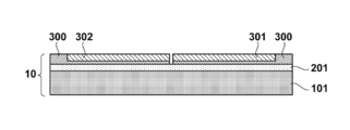
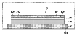
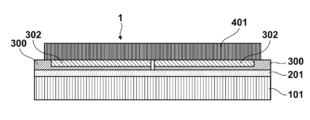
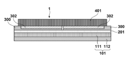
- the figure which shows the radiation detection apparatus of one Embodiment of this invention The figure which shows the manufacturing method of the radiation detection apparatus of one Embodiment of this invention.
- the figure which shows the manufacturing method of the radiation detection apparatus of one Embodiment of this invention The figure which shows the manufacturing method of the radiation detection apparatus of one Embodiment of this invention.
- the figure which shows the principle of disappearance of a bubble The figure which shows the radiation detection apparatus of other embodiment of this invention.
- the figure which shows the radiation detection apparatus of other embodiment of this invention. The figure which shows the radiation detection apparatus of other embodiment of this invention.
- the figure which shows the radiation detection apparatus of other embodiment of this invention The figure which shows the radiation detection apparatus of other embodiment of this invention.
- the figure which shows the radiation detection apparatus of other embodiment of this invention The figure which shows the radiation detection apparatus of other embodiment of this invention.
- the figure which shows the radiation detection apparatus of other embodiment of this invention The figure which shows the radiation detection apparatus of other embodiment of this invention
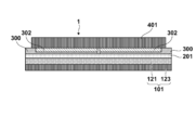
- FIG. 1 schematically shows a radiation detection apparatus 1 according to one embodiment of the present invention.
- the radiation detection apparatus 1 includes a support substrate 101, one or more sensor substrates 300 on which photoelectric conversion units 302 are formed, a scintillator layer 401, and a bonding layer 201 that couples the support substrate 101 and the sensor substrate 300.
- the support substrate 101 has a discharge path 150 for discharging bubbles between the support substrate 101 and the sensor substrate 300, and is formed between the support substrate 101 and the sensor substrate 300 during the production of the radiation detection apparatus 1. The air bubbles are discharged through the discharge path 150.
- bubbles are formed at the boundary surface between the bonding layer 201 and the support substrate 101 when the sensor substrate 300 is bonded to the support substrate 101 by the bonding layer 201 after the scintillator layer 401 is formed on the sensor substrate 300. Can be done.
- the implementation form of the discharge path 150 provided in the support substrate 101 may include various forms. Bubbles can also be formed at the interface between the bonding layer 201 and the sensor substrate 300 when the sensor substrate 300 is bonded to the support substrate 101 by the bonding layer 201. Bubbles at the boundary surface between the bonding layer 201 and the sensor substrate 300 can be discharged through the plurality of through holes and the discharge path 150 of the support substrate 101 by using the bonding layer 201 including the plurality of through holes.
- the ratio R1 of the area of the contact portion between the sensor substrate 300 and the bonding layer 201 in the area of the adhesion target region of the sensor substrate 300 can be, for example, 5 to 80%.
- (1-R1) is the ratio of the area of the discharge portion 150 exposed on the surface of the bonding layer 201 on the sensor substrate 300 side.
- the ratio R2 of the area of the contact portion between the support substrate 101 and the bonding layer 201 in the area of the bonding target region of the support substrate 101 can be, for example, 5 to 80%.
- (1-R2) is the ratio of the area of the discharge path 150 exposed on the surface of the bonding layer 201 on the support substrate 101 side.
- the ratio R2 exceeds 80%, the efficiency of discharging the gas from the bubbles decreases, and the bubbles can be left behind. If the ratio R2 is less than 5%, the bonding force is low, and peeling may occur between the support substrate 101 and the sensor substrate 300.
- the discharge path 150 of the support substrate 101 requires about 2 minutes in a system using a general rotary pump or dry pump in order to reduce the pressure from atmospheric pressure to a vacuum pressure of about 1 ⁇ 10 ⁇ 2 Pa. It can be determined in consideration. That is, the discharge path 150 can be designed so that the gas can move through the discharge path 150 following a pressure change of about 1 ⁇ 10 5 Pa in 2 minutes.
- the discharge path 150 can be provided, for example, by configuring the support substrate 101 with a porous structure portion in which a large number of micropores are randomly dispersed. Alternatively, the discharge path 150 may be formed in a regular pattern by machining or laser processing the material substrate of the support substrate 101.
- the material of the support substrate 101 for example, a metal, a metal compound, ceramic, or a heat resistant resin can be selected.
- the material of the support substrate 101 may be, for example, a carbon-based material (for example, CFRP, a-Carbon, PEEK, or PPS).
- the support substrate 101 may be a porous aluminum plate or a porous alumina plate.
- a porous aluminum plate or a porous alumina plate is available from, for example, Gwangyang Shoko Co., Ltd.
- the support substrate 101 may have a corrugated surface so that a plurality of flow paths are configured as the discharge paths 150 between the support substrate 101 and the bonding layer 201.
- the support substrate 101 having the discharge path as described above has a secondary effect that its weight is reduced.
- the bonding layer 201 can have heat resistance such that the bonding between the support substrate 101 and the sensor substrate 300 by the bonding layer 201 is maintained at 200 ° C., for example.
- the scintillator layer 401 can be formed at a temperature of, for example, 200 ° C. or less by an evaporation method after the support substrate 101 and the sensor substrate 300 are bonded by the bonding layer 201.
- the bonding layer 201 can be made of, for example, an acrylic resin, a silicone resin, an epoxy resin, or polyimide.
- the bonding layer 201 may be one in which an adhesive layer is disposed on both sides of the base material.
- a condition for allowing bubbles between the bonding layer 201 and the sensor substrate 300 to pass through the bonding layer 201 and travel toward the support substrate 101 will be considered.
- the bonding layer 201 when the thickness of the bonding layer 201 is 25 ⁇ m, the bonding layer 201 preferably has a gas permeability of 0.02 cc / (m ⁇ 24 hours) / atm or more.
- the gas permeability of the bonding layer 201 is 0.02 cc / (m ⁇ 24 hours) / atm or more, when the bonded body 10 of the support substrate 101 and the sensor substrate 300 by the bonding layer 201 is placed in a vacuum environment, the diameter is 5 mm.
- the bubbles having a thickness of 2 ⁇ m can pass through the bonding layer 201 and reach the support substrate 101.
- the gas permeation amount V can be calculated by the following equation.
- V QPST / d (cc)
- V is a gas permeation amount (cc)
- Q is a gas permeation coefficient (cc / (m ⁇ day) / atm)
- P is a pressure difference (atm)
- S is a permeation area (m 2 )
- T is time ( D)
- d is the thickness of the bonding layer (m) It is.
- Examples of a material suitable for obtaining a gas permeability of 0.02 cc / (m ⁇ 24 hours) / atm or more include the following materials. Figures in parentheses are oxygen gas permeability. The unit is (cc / (m ⁇ 24 hours) / atm).
- Nylon 12 0.0275) Polyurethane (0.0675) Polyvinyl chloride (0.091) Polycarbonate (0.09) Polystyrene (0.2025) Silicone (36) Butyl cellulose acetate (0.345) ABS resin (0.048) Polyethylene (0.0725) Polypropylene (0.162) Ethylcellulose (0.875) As exemplarily shown in FIG.
- a plurality of sensor substrates 300 may be arranged (tiled) on a support substrate 101 via a bonding layer 201.
- the sensor substrate 300 may be, for example, a semiconductor substrate in which the photoelectric conversion unit 302 is formed, or may be an insulating substrate such as a glass substrate on which the photoelectric conversion unit is formed. A substrate having another structure may be used.
- the scintillator layer 401 is a layer that converts radiation into light, and is formed on one or a plurality of sensor substrates 300 by vapor deposition.
- the radiation detection apparatus 1 includes a support substrate 101 made of a porous aluminum plate or a porous alumina plate, a bonding layer 201 made of a heat-resistant adhesive, a plurality of sensor substrates 300 made of a CMOS image sensor, and a scintillator.
- Layer 401 is composed of CsI.
- bubbles 221 and 222 may exist at the interface between the bonding layer 201 and the bonding layer 201.
- the pressure in the vacuum chamber is reduced to a pressure lower than the atmospheric pressure
- the pressure of the bubbles 221 and 222 (1 atm) and the vacuum pressure for example, rotary
- the gas constituting the bubbles 221 and 222 is discharged through the discharge path of the support substrate 101 due to the difference from about 0.1 atm when exhausted by the pump for about 2 minutes.
- the bubbles 221 and 222 disappear.
- the bonding layer 201 when a pressure-sensitive adhesive having a thickness of 25 ⁇ m is used as the bonding layer 201, if the bonding layer 201 has a gas permeability of 0.02 cc / (m ⁇ 24 hours) / atm or more, the thickness is 5 mm. However, bubbles of about 2 ⁇ m can be removed.
- the manufacturing method of the radiation detection apparatus 1 will be exemplarily described with reference to FIGS. 2A and 2B.
- first step shown in FIG. 2A one or a plurality of sensor substrates 300 on which the photoelectric conversion units 302 are formed and the support substrate 101 are bonded by the bonding layer 201 to form the bonded body 10.
- the periphery of the combined body 10 is depressurized to a pressure lower than atmospheric pressure (typically vacuum pressure).
- the second step can be performed by placing the bonded body 10 in the vacuum chamber 500 of the vapor deposition apparatus and depressurizing the vacuum chamber 500.
- the combination 10 can be placed in the load lock chamber and the load lock chamber can be depressurized. Thereafter, the combined body 10 is transferred from the load lock chamber into the vacuum chamber (processing chamber) 500.
- the second step by reducing the pressure around the combined body 10 to a pressure lower than the atmospheric pressure, it exists at the boundary surface between the support substrate 101 and the bonding layer 201 and / or the boundary surface between the sensor substrate 300 and the bonding layer 201.
- the gas constituting the bubbles is discharged through the discharge path of the support substrate 101.
- a scintillator layer 401 is formed on the sensor substrate 300 by a vapor deposition method in a vacuum chamber 500 having a reduced pressure.
- the environment surrounding the combination 10 is reduced in the vacuum chamber 500 for forming the scintillator layer 401 on the sensor substrate 300 of the combination 10 or the load lock chamber connected thereto. Bubbles are removed. This eliminates the need for an additional bubble removal step and simplifies the manufacturing process.
- the bonding layer 201 may have a plurality of through holes. When such a bonding layer 201 is used, the material of the bonding layer 201 can be selected without considering the bubble transmittance.
- the discharge path of the support substrate 101 may be configured by a plurality of holes that penetrate the support substrate 101 in a direction orthogonal to the boundary surface between the support substrate 101 and the bonding layer 201.
- the support substrate 101 may include a portion 111 having a plurality of vertical holes and a plurality of horizontal holes constituting the discharge path. Portion 111 can be supported by portion 112. The portion 112 may be a portion that is stronger than the portion 111.
- the plurality of vertical holes extend from the boundary surface into the support substrate 101 in a direction perpendicular to the boundary surface between the support substrate 101 and the bonding layer 201.
- the plurality of lateral holes extend through the support substrate 101 in a direction parallel to the boundary surface and reach the side surface of the support substrate 101.
- the support substrate 101 may include a porous structure part 121 and a non-porous structure part 122 that constitute a discharge path.
- the porous structure part 121 is disposed so as to contact the bonding layer 201
- the non-porous structure part 122 is disposed on the side opposite to the side where the porous structure part 121 contacts the bonding layer 201.
- the support substrate 101 includes a porous structure portion 121 and a vertical hole portion 123 having a plurality of vertical holes extending in a direction perpendicular to the contact surface between the support substrate 101 and the bonding layer 201. You may have.
- the porous structure portion 121 is disposed so as to contact the bonding layer 201, and the vertical hole portion 123 is disposed on the side opposite to the side where the porous structure portion 121 contacts the bonding layer 201.
- the carry-out path of the support substrate 101 is configured by a hole in the porous structure 121 and a plurality of vertical holes in the vertical hole 123.
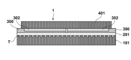
- the discharge path of the support substrate 101 includes a plurality of grooves formed along the boundary surface on the side of the boundary surface between the support substrate 101 and the bonding layer 201 in the support substrate 101. T may be included.
- FIG. 6A is a cross-sectional view of the radiation detection apparatus 1
- FIG. 6B is a plan view of the support substrate 101.
- the support substrate 101 may have a corrugated surface so that a discharge path is formed at the boundary surface between the support substrate 101 and the coupling layer 201.
Landscapes
- Physics & Mathematics (AREA)
- Health & Medical Sciences (AREA)
- Life Sciences & Earth Sciences (AREA)
- General Physics & Mathematics (AREA)
- High Energy & Nuclear Physics (AREA)
- Molecular Biology (AREA)
- Spectroscopy & Molecular Physics (AREA)
- Measurement Of Radiation (AREA)
Abstract
放射線検出装置の製造方法は、光電変換部が形成されたセンサ基板と支持基板とを結合層によって結合して結合体を形成する第1工程と、前記第1工程の後に前記結合体の周囲を大気圧よりも低い圧力まで減圧する第2工程と、前記第2工程の後に前記センサ基板の上に蒸着法によってシンチレータ層を形成する第3工程と、を含み、前記支持基板は、前記支持基板と前記センサ基板との間の気泡を排出するための排出路を有し、前記第2工程において前記支持基板と前記センサ基板との間の気泡を構成する気体が前記排出路を通して排出される。
Description
本発明は、放射線検出装置およびその製造方法に関する。
光電変換素子アレイの上にシンチレータ層が配置された放射線検出装置が知られている。特許文献1には、基板と、該基板の上に配置された光電変換素子アレイと、該光電変換素子アレイの上に配置されたシンチレータ層とを含むセンサパネルを接着層によって支持部材に接着した放射線検出装置が記載されている。該接着層は、接着面に形成された気泡を消失させるために、多孔質構造を有する樹脂層で構成されている。
上記の放射線検出装置の製造において、接着面に発生した気泡を効果的に除去するために、センサパネルを接着層によって支持部材に接着した構造体を形成した後に、該構造体を減圧環境下に置くことが考えられる。これにより、接着面に形成された気泡を効果的に除去することができると考えられる。しかしながら、基板、光電変換素子アレイおよびシンチレータ層の積層構造からなるセンサパネルを接着層によって支持部材に接着した構造体を形成した後に該構造体を気泡の除去のために真空チャンバに入れることは、製造工程の複雑化をもたらす。
本発明は、上記の課題認識を契機としてなされたものであり、放射線検出装置の製造工程の簡単化に有利な技術を提供することを目的とする。
本発明の1つの側面は、放射線検出装置の製造方法を対象とし、前記製造方法は、光電変換部が形成されたセンサ基板と支持基板とを結合層によって結合して結合体を形成する第1工程と、前記第1工程の後に前記結合体の周囲を大気圧よりも低い圧力まで減圧する第2工程と、前記第2工程の後に前記センサ基板の上に蒸着法によってシンチレータ層を形成する第3工程と、を含み、前記支持基板は、前記支持基板と前記センサ基板との間の気泡を排出するための排出路を有し、前記第2工程において前記支持基板と前記センサ基板との間の気泡を構成する気体が前記排出路を通して排出される。
本発明によれば、放射線検出装置の製造工程の簡単化に有利な技術が提供される。
以下、添付図面を参照しながら本発明の例示的な実施形態を通して説明する。
図1には、本発明の1つの実施形態の放射線検出装置1が模式的に示されている。符号Bで示された部分には、支持基板101の部分Aが拡大して示されている。放射線検出装置1は、支持基板101と、光電変換部302が形成された1又は複数のセンサ基板300と、シンチレータ層401と、支持基板101とセンサ基板300とを結合する結合層201とを有する。支持基板101は、支持基板101とセンサ基板300との間の気泡を排出するための排出路150を有し、放射線検出装置1の製造途中で支持基板101とセンサ基板300との間に形成された気泡は、排出路150を通して排出される。
ここで、気泡は、センサ基板300の上にシンチレータ層401が形成された後にセンサ基板300を結合層201によって支持基板101に結合させる際に、結合層201と支持基板101との境界面に形成されうる。支持基板101に設けられる排出路150の実施形式は、種々の形式を含みうる。気泡はまた、センサ基板300を結合層201によって支持基板101に結合させる際に、結合層201とセンサ基板300との境界面にも形成されうる。結合層201とセンサ基板300との境界面の気泡は、複数の貫通孔を含む結合層201を使用することによって、当該複数の貫通孔および支持基板101の排出路150を通して排出されうる。
センサ基板300の接着対象領域の面積に占めるセンサ基板300と結合層201との接触部分の面積の比率R1は、例えば、5~80%でありうる。(1-R1)は、結合層201のセンサ基板300の側の表面に露出している排出部150の面積の比率である。同様に、支持基板101の接着対象領域の面積に占める支持基板101と結合層201との接触部分の面積の比率R2は、例えば、5~80%でありうる。(1-R2)は、結合層201の支持基板101の側の表面に露出している排出路150の面積の比率である。比率R2が80%を超えると、気泡からの気体の排出効率が低下し、気泡が取り残されうる。比率R2が5%に満たないと、結合力が低く、支持基板101とセンサ基板300との間に剥がれが生じうる。
支持基板101の排出路150は、例えば、大気圧から1×10⁻²Pa程度の真空圧力まで減圧するために、一般的なロータリーポンプまたはドライポンプを使ったシステムで2分程度を要することを考慮して決定されうる。つまり、2分間における約1×10⁵Paの圧力変化に追随して排出路150を気体が移動できるように排出路150が設計されうる。排出路150は、例えば、多数の微小孔がランダムに分散した多孔質構造部で支持基板101を構成することによって提供されうる。あるいは、排出路150は、支持基板101の材料基板を機械加工またはレーザー加工することによって規則的なパターンで構成されうる。
支持基板101の材料としては、例えば、金属、金属化合物、セラミックまたは耐熱樹脂が選択されうる。あるいは、支持基板101の材料は、例えば、炭素系素材(例えば、CFRP、a-Carbon、PEEKまたはPPS)であってもよい。あるいは、支持基板101は、ポーラスアルミ板またはポーラスアルミナ板であってもよい。ポーラスアルミ板またはポーラスアルミナ板は、例えば、広陽商工株式会社から入手可能である。あるいは、支持基板101は、支持基板101と結合層201との間に排出路150として複数の流路が構成されるように、波打った表面を有してもよい。以上のような排出路を有する支持基板101は、その重量が軽量化されるという副次的な効果を奏する。
結合層201は、例えば、200℃において結合層201による支持基板101とセンサ基板300との結合が維持されるような耐熱性を有しうる。ここで、シンチレータ層401の形成は、支持基板101とセンサ基板300とが結合層201によって結合された後に、蒸着法によって、例えば200℃以下の温度でなされうる。
結合層201は、例えば、アクリル系樹脂、シリコーン系樹脂、エポキシ系樹脂またはポリイミドで構成されうる。結合層201は、基材の両面に接着層が配置されたものでもよい。ここで、結合層201とセンサ基板300との間の気泡が結合層201を通過して支持基板101に向かって進むための条件を考える。一例において、結合層201の厚さが25μmであれば、結合層201が0.02cc/(m・24時間)/atm以上の気体透過率を有することが好ましい。結合層201の気体透過率が0.02cc/(m・24時間)/atm以上であれば、結合層201による支持基板101とセンサ基板300との結合体10を真空環境におくと、直径5mm、厚さ2μmの気泡は結合層201を通過して支持基板101に到達しうる。
気体透過量Vは、以下の式で計算されうる。
V=QPST/d (cc)
ここで、Vは気体透過量(cc)、Qは気体透過係数(cc/(m・日)/atm)、Pは圧力差(atm)、Sは透過面積(m2)、Tは時間(日)、dは結合層の厚さ(m)
である。
ここで、Vは気体透過量(cc)、Qは気体透過係数(cc/(m・日)/atm)、Pは圧力差(atm)、Sは透過面積(m2)、Tは時間(日)、dは結合層の厚さ(m)
である。
0.02cc/(m・24時間)/atm以上の気体透過率を得るために好適な材料として、例えば、以下の材料を挙げることができる。( )内は、酸素の気体透過率。単位は(cc/(m・24時間)/atm)である。
ナイロン12 (0.0275)
ポリウレタン (0.0675)
ポリ塩化ビニル (0.091)
ポリカーボネート (0.09)
ポリスチレン (0.2025)
シリコーン (36)
酢酸ブチルセルロース (0.345)
ABS樹脂 (0.048)
ポリエチレン (0.0725)
ポリプロピレン (0.162)
エチルセルロース (0.875)
図1に例示的に示されているように、複数のセンサ基板300が支持基板101の上に結合層201を介して配置(タイリング)されてもよい。センサ基板300は、例えば、その内部に光電変換部302が形成された半導体基板であってもよいし、その上に光電変換部が形成されたガラス基板等の絶縁性基板であってもよいし、他の構造を有する基板であってもよい。シンチレータ層401は、放射線を光に変換する層であり、1又は複数のセンサ基板300の上に蒸着法によって形成される。
ナイロン12 (0.0275)
ポリウレタン (0.0675)
ポリ塩化ビニル (0.091)
ポリカーボネート (0.09)
ポリスチレン (0.2025)
シリコーン (36)
酢酸ブチルセルロース (0.345)
ABS樹脂 (0.048)
ポリエチレン (0.0725)
ポリプロピレン (0.162)
エチルセルロース (0.875)
図1に例示的に示されているように、複数のセンサ基板300が支持基板101の上に結合層201を介して配置(タイリング)されてもよい。センサ基板300は、例えば、その内部に光電変換部302が形成された半導体基板であってもよいし、その上に光電変換部が形成されたガラス基板等の絶縁性基板であってもよいし、他の構造を有する基板であってもよい。シンチレータ層401は、放射線を光に変換する層であり、1又は複数のセンサ基板300の上に蒸着法によって形成される。
一例において、放射線検出装置1は、支持基板101がポーラスアルミ板またはポーラスアルミナ板で構成され、結合層201が耐熱性粘着剤で構成され、複数のセンサ基板300がCMOSイメージセンサで構成され、シンチレータ層401がCsIで構成される。
センサ基板300と支持基板101とを結合層201によって結合して結合体10を構成した直後は、図3に模式的に示すように、支持基板101と結合層201との境界面およびセンサ基板300と結合層201との境界面に気泡221、222が存在しうる。しかし、シンチレータ層401を形成するために結合体10を真空チャンバに入れて真空チャンバ内を大気圧よりも低い圧力まで減圧すると、気泡221、222の圧力(1気圧)と真空圧力(例えば、ロータリーポンプで2分ほど排気すると約0.1気圧になる。)との差によって気泡221、222を構成する気体が支持基板101の排出路を通して排出される。これにより気泡221、222が消滅する。
例えば、結合層201として25μmの厚さを有する粘着剤を用いた場合、結合層201が0.02cc/(m・24時間)/atm以上の気体透過率を有すると、半径が5mmで厚さが2μm程度の気泡は除去されうる。
以下、図2A、2Bを参照しながら放射線検出装置1の製造方法を例示的に説明する。まず、図2Aに示す第1工程において、光電変換部302が形成された1又は複数のセンサ基板300と支持基板101とを結合層201によって結合して結合体10を形成する。
その後、図2Bに示す第2工程において、結合体10の周囲を大気圧よりも低い圧力(典型的には真空圧力)まで減圧する。典型的には、第2工程は、蒸着装置の真空チャンバ500内に結合体10を配置し、真空チャンバ500内を減圧することによってなされうる。あるいは、蒸着装置がロードロックチャンバを備える場合、結合体10をロードロックチャンバに入れ、ロードロックチャンバを減圧することによってなされうる。その後、ロードロックチャンバから真空チャンバ(処理チャンバ)500内に結合体10が搬送される。
第2工程において結合体10の周囲を大気圧よりも低い圧力まで減圧することにより、支持基板101と結合層201との境界面および/またはセンサ基板300と結合層201との境界面に存在する気泡を構成する気体が支持基板101の排出路を通して排出される。
その後、図2Cに示す第3工程において、減圧された真空チャンバ500の中で、センサ基板300の上に蒸着法によってシンチレータ層401を形成する。このように、この実施形態では、結合体10のセンサ基板300の上にシンチレータ層401を形成するための真空チャンバ500またはそれに接続されたロードロックチャンバにおいて結合体10を取り巻く環境を減圧することにより気泡が除去される。これにより、付加的な気泡の除去工程が不要になり、製造工程を単純化することができる。
図4Aに模式的に示されるように、結合層201は、複数の貫通孔を有してもよい。このような結合層201を使用する場合、気泡透過率を考慮することなく結合層201の材料を選択することができる。図4Bに模式的に示すように、支持基板101の排出路は、支持基板101と結合層201との境界面に直交する方向に支持基板101を貫通した複数の孔で構成されてもよい。図4Cに模式的に示すように、支持基板101は、排出路を構成する複数の縦孔および複数の横孔を有する部分111を含んでもよい。部分111は、部分112によって支持されうる。部分112は、部分111よりも強度が高い部分でありうる。前記複数の縦孔は、支持基板101と結合層201との境界面に直交する方向に該境界面から支持基板101の中に延びる。前記複数の横孔は、前記境界面に平行な方向に支持基板101の中を延びて支持基板101の側面に至る。
図5Aに模式的に示すように、支持基板101は、排出路を構成する多孔質構造部121と、非多孔質構造部122とを含んでもよい。ここで、多孔質構造部121は、結合層201に接触するように配置され、非多孔質構造部122は、多孔質構造部121が結合層201に接触する側とは反対側に配置される。図5Bに模式的に示すように、支持基板101は、多孔質構造部121と、支持基板101と結合層201との接触面に直交する方向に延びた複数の縦孔を有する縦孔部123とを有してもよい。ここで、多孔質構造部121は、結合層201に接触するように配置され、縦孔部123は、多孔質構造部121が結合層201に接触する側とは反対側に配置される。支持基板101の搬出路は、多孔質構造部121の孔および縦孔部123の複数の縦孔によって構成される。
図6A、6Bに模式的に示すように、支持基板101の排出路は、支持基板101における支持基板101と結合層201との境界面の側に該境界面に沿って形成された複数の溝Tを含んでもよい。ここで、図6Aは、放射線検出装置1の断面図、図6Bは支持基板101の平面図である。図7に模式的に示すように、支持基板101は、支持基板101と結合層201との境界面に排出路が構成されるように、波打った表面を有してもよい。
本発明は上記実施の形態に制限されるものではなく、本発明の精神及び範囲から離脱することなく、様々な変更及び変形が可能である。従って、本発明の範囲を公にするために、以下の請求項を添付する。
本願は、2013年8月29日提出の日本国特許出願特願2013-178564を基礎として優先権を主張するものであり、その記載内容の全てを、ここに援用する。
Claims (16)
- 放射線検出装置の製造方法であって、
光電変換部が形成されたセンサ基板と支持基板とを結合層によって結合して結合体を形成する第1工程と、
前記第1工程の後に前記結合体の周囲を大気圧よりも低い圧力まで減圧する第2工程と、
前記第2工程の後に前記センサ基板の上に蒸着法によってシンチレータ層を形成する第3工程と、を含み、
前記支持基板は、前記支持基板と前記センサ基板との間の気泡を排出するための排出路を有し、前記第2工程において前記支持基板と前記センサ基板との間の気泡を構成する気体が前記排出路を通して排出される、
ことを特徴とする放射線検出装置の製造方法。 - 前記支持基板は、前記排出路を構成する多孔質構造部を含む、
ことを特徴とする請求項1に記載の放射線検出装置の製造方法。 - 前記排出路は、前記支持基板と前記結合層との境界面に直交する方向に前記支持基板を貫通した複数の孔を含む、
ことを特徴とする請求項1に記載の放射線検出装置の製造方法。 - 前記排出路は、前記支持基板と前記結合層との境界面に直交する方向に前記境界面から前記支持基板の中に延びた複数の縦孔と、前記境界面に平行な方向に前記支持基板の中を延びて前記支持基板の側面に至る複数の横孔とを含む、
ことを特徴とする請求項1に記載の放射線検出装置の製造方法。 - 前記支持基板は、前記排出路を構成する多孔質構造部と、非多孔質構造部とを含み、前記多孔質構造部は、前記結合層に接触するように配置され、前記非多孔質構造部は、前記多孔質構造部が前記結合層に接触する側とは反対側に配置されている、
ことを特徴とする請求項1に記載の放射線検出装置の製造方法。 - 前記支持基板は、多孔質構造部と、前記支持基板と前記結合層との接触面に直交する方向に延びた複数の縦孔を有する縦孔部とを有し、前記多孔質構造部は、前記結合層に接触するように配置され、前記縦孔部は、前記多孔質構造部が前記結合層に接触する側とは反対側に配置され、前記多孔質構造部の孔および前記縦孔部の前記複数の縦孔によって前記排出路が構成される、
ことを特徴とする請求項1に記載の放射線検出装置の製造方法。 - 前記排出路は、前記支持基板における前記支持基板と前記結合層との境界面の側に前記境界面に沿って形成された複数の溝を含む、
ことを特徴とする請求項1に記載の放射線検出装置の製造方法。 - 前記支持基板は、前記支持基板と前記結合層との境界面に前記排出路が構成されるように、波打った表面を有する、
ことを特徴とする請求項1に記載の放射線検出装置の製造方法。 - 前記結合層は、複数の貫通孔を含む、
ことを特徴とする請求項1乃至8のいずれか1項に記載の放射線検出装置の製造方法。 - 前記第1工程では、複数の前記センサ基板と前記支持基板とを前記結合層によって結合して前記結合体を形成する、
ことを特徴とする請求項1乃至9のいずれか1項に記載の放射線検出装置の製造方法。 - 支持基板と、光電変換部が形成されたセンサ基板と、シンチレータ層とを有する放射線検出装置であって、
前記支持基板と前記センサ基板とが結合層によって結合され、
前記支持基板は、多数の微小孔がランダムに分散した多孔質構造部を含む、
ことを特徴とする放射線検出装置。 - 支持基板と、光電変換部が形成されたセンサ基板と、シンチレータ層とを有する放射線検出装置であって、
前記支持基板と前記センサ基板とが結合層によって結合され、
前記支持基板は、前記支持基板と前記結合層との境界面に直交する方向に前記境界面から前記支持基板の中に延びた複数の縦孔と、前記境界面に平行な方向に前記支持基板の中を延びて前記支持基板の側面に至る複数の横孔とを含む、
ことを特徴とする放射線検出装置。 - 支持基板と、光電変換部が形成されたセンサ基板と、シンチレータ層とを有する放射線検出装置であって、
前記支持基板と前記センサ基板とが結合層によって結合され、
前記支持基板は、多孔質構造部と、前記支持基板と前記結合層との接触面に直交する方向に延びた複数の縦孔を有する縦孔部とを有し、前記多孔質構造部は、前記結合層に接触するように配置され、前記縦孔部は、前記多孔質構造部が前記結合層に接触する側とは反対側に配置されている、
ことを特徴とする放射線検出装置。 - 支持基板と、光電変換部が形成されたセンサ基板と、シンチレータ層とを有する放射線検出装置であって、
前記支持基板と前記センサ基板とが結合層によって結合され、
前記支持基板は、前記支持基板と前記結合層との境界面の側に、前記境界面に沿って形成された複数の溝を含む、
ことを特徴とする放射線検出装置。 - 支持基板と、光電変換部が形成されたセンサ基板と、シンチレータ層とを有する放射線検出装置であって、
前記支持基板と前記センサ基板とが結合層によって結合され、
前記支持基板は、前記支持基板と前記結合層との間に複数の流路が構成されるように、波打った表面を有する、
ことを特徴とする放射線検出装置。 - 前記結合層は、複数の貫通孔を含む、
ことを特徴とする請求項11乃至15のいずれか1項に記載の放射線検出装置。
Applications Claiming Priority (2)
| Application Number | Priority Date | Filing Date | Title |
|---|---|---|---|
| JP2013178564A JP6180242B2 (ja) | 2013-08-29 | 2013-08-29 | 放射線検出装置およびその製造方法 |
| JP2013-178564 | 2013-08-29 |
Publications (1)
| Publication Number | Publication Date |
|---|---|
| WO2015029358A1 true WO2015029358A1 (ja) | 2015-03-05 |
Family
ID=52585953
Family Applications (1)
| Application Number | Title | Priority Date | Filing Date |
|---|---|---|---|
| PCT/JP2014/004184 Ceased WO2015029358A1 (ja) | 2013-08-29 | 2014-08-13 | 放射線検出装置およびその製造方法 |
Country Status (2)
| Country | Link |
|---|---|
| JP (1) | JP6180242B2 (ja) |
| WO (1) | WO2015029358A1 (ja) |
Families Citing this family (1)
| Publication number | Priority date | Publication date | Assignee | Title |
|---|---|---|---|---|
| JP6906687B2 (ja) | 2018-03-19 | 2021-07-21 | 富士フイルム株式会社 | 放射線検出器及び放射線画像撮影装置 |
Citations (6)
| Publication number | Priority date | Publication date | Assignee | Title |
|---|---|---|---|---|
| JP2005195643A (ja) * | 2003-12-26 | 2005-07-21 | Canon Inc | 放射線画像撮影装置 |
| JP2005214800A (ja) * | 2004-01-29 | 2005-08-11 | Hamamatsu Photonics Kk | 放射線イメージセンサ |
| JP2005214808A (ja) * | 2004-01-29 | 2005-08-11 | Hamamatsu Photonics Kk | 放射線イメージセンサおよびその製造方法 |
| JP2008224429A (ja) * | 2007-03-13 | 2008-09-25 | Canon Inc | 放射線検出装置 |
| JP2010098133A (ja) * | 2008-10-16 | 2010-04-30 | Shimadzu Corp | 光マトリックスデバイスの製造方法および光マトリックスデバイス |
| JP2012133315A (ja) * | 2010-11-29 | 2012-07-12 | Fujifilm Corp | 放射線撮影装置 |
-
2013
- 2013-08-29 JP JP2013178564A patent/JP6180242B2/ja not_active Expired - Fee Related
-
2014
- 2014-08-13 WO PCT/JP2014/004184 patent/WO2015029358A1/ja not_active Ceased
Patent Citations (6)
| Publication number | Priority date | Publication date | Assignee | Title |
|---|---|---|---|---|
| JP2005195643A (ja) * | 2003-12-26 | 2005-07-21 | Canon Inc | 放射線画像撮影装置 |
| JP2005214800A (ja) * | 2004-01-29 | 2005-08-11 | Hamamatsu Photonics Kk | 放射線イメージセンサ |
| JP2005214808A (ja) * | 2004-01-29 | 2005-08-11 | Hamamatsu Photonics Kk | 放射線イメージセンサおよびその製造方法 |
| JP2008224429A (ja) * | 2007-03-13 | 2008-09-25 | Canon Inc | 放射線検出装置 |
| JP2010098133A (ja) * | 2008-10-16 | 2010-04-30 | Shimadzu Corp | 光マトリックスデバイスの製造方法および光マトリックスデバイス |
| JP2012133315A (ja) * | 2010-11-29 | 2012-07-12 | Fujifilm Corp | 放射線撮影装置 |
Also Published As
| Publication number | Publication date |
|---|---|
| JP6180242B2 (ja) | 2017-08-16 |
| JP2015049045A (ja) | 2015-03-16 |
Similar Documents
| Publication | Publication Date | Title |
|---|---|---|
| TWI467691B (zh) | Electrostatic chuck and its manufacturing method | |
| JP2008311635A5 (ja) | ||
| CN104169657B (zh) | 排气阵列及制造方法 | |
| EP3239115B1 (en) | Heat transport structure and manufacturing method therefor | |
| JP5941821B2 (ja) | 通気性シート、吸着ユニットへの作業対象物の吸着方法、およびセラミックコンデンサの製造方法 | |
| JP2010099826A (ja) | 吸着用シート | |
| EP1633002A3 (en) | Semiconductor device, semiconductor module, and manufacturing method of semiconductor device | |
| JP2017014620A (ja) | 蒸着マスクの製造方法、蒸着マスク準備体、有機半導体素子の製造方法、及び蒸着マスク | |
| CN104591075A (zh) | 保护微机电系统麦克风声音端口及其在晶片级形成的方法 | |
| US20150143874A1 (en) | Sensor device | |
| CN107250807B (zh) | 半导体装置及其制造方法 | |
| CN111108758B (zh) | Mems麦克风系统 | |
| JP2017515301A5 (ja) | ||
| JP6180242B2 (ja) | 放射線検出装置およびその製造方法 | |
| JP6853114B2 (ja) | 吸着用部材 | |
| JP2010528300A5 (ja) | ||
| KR102386746B1 (ko) | 기판 캐리어 | |
| JP2015068653A (ja) | 放射線撮像装置、その製造方法及び放射線検査装置 | |
| JP2011142213A (ja) | 薄膜電子素子の個片化方法及びその方法により製造された電子素子搭載粘着性シート | |
| TWI666783B (zh) | 製造光學感測器配置之方法和用於光學感測器之殼體 | |
| US10036814B2 (en) | X-ray detector with directly applied scintillator | |
| CN113631246A (zh) | 透气孔用构件、具有透气孔用构件的电子器件的制造方法以及构件供给用带 | |
| CN113557139B (zh) | 构件供给用片材 | |
| JP2015049045A5 (ja) | ||
| CN111433388A (zh) | 基板用保护具以及附膜基板的制造方法 |
Legal Events
| Date | Code | Title | Description |
|---|---|---|---|
| 121 | Ep: the epo has been informed by wipo that ep was designated in this application |
Ref document number: 14840516 Country of ref document: EP Kind code of ref document: A1 |
|
| NENP | Non-entry into the national phase |
Ref country code: DE |
|
| 122 | Ep: pct application non-entry in european phase |
Ref document number: 14840516 Country of ref document: EP Kind code of ref document: A1 |