WO2015029337A1 - 表示制御装置 - Google Patents
表示制御装置 Download PDFInfo
- Publication number
- WO2015029337A1 WO2015029337A1 PCT/JP2014/004057 JP2014004057W WO2015029337A1 WO 2015029337 A1 WO2015029337 A1 WO 2015029337A1 JP 2014004057 W JP2014004057 W JP 2014004057W WO 2015029337 A1 WO2015029337 A1 WO 2015029337A1
- Authority
- WO
- WIPO (PCT)
- Prior art keywords
- image data
- light
- value
- average
- data
- Prior art date
- Legal status (The legal status is an assumption and is not a legal conclusion. Google has not performed a legal analysis and makes no representation as to the accuracy of the status listed.)
- Ceased
Links
Images






Classifications
-
- G—PHYSICS
- G09—EDUCATION; CRYPTOGRAPHY; DISPLAY; ADVERTISING; SEALS
- G09G—ARRANGEMENTS OR CIRCUITS FOR CONTROL OF INDICATING DEVICES USING STATIC MEANS TO PRESENT VARIABLE INFORMATION
- G09G3/00—Control arrangements or circuits, of interest only in connection with visual indicators other than cathode-ray tubes
- G09G3/20—Control arrangements or circuits, of interest only in connection with visual indicators other than cathode-ray tubes for presentation of an assembly of a number of characters, e.g. a page, by composing the assembly by combination of individual elements arranged in a matrix no fixed position being assigned to or needed to be assigned to the individual characters or partial characters
- G09G3/22—Control arrangements or circuits, of interest only in connection with visual indicators other than cathode-ray tubes for presentation of an assembly of a number of characters, e.g. a page, by composing the assembly by combination of individual elements arranged in a matrix no fixed position being assigned to or needed to be assigned to the individual characters or partial characters using controlled light sources
- G09G3/30—Control arrangements or circuits, of interest only in connection with visual indicators other than cathode-ray tubes for presentation of an assembly of a number of characters, e.g. a page, by composing the assembly by combination of individual elements arranged in a matrix no fixed position being assigned to or needed to be assigned to the individual characters or partial characters using controlled light sources using electroluminescent panels
- G09G3/32—Control arrangements or circuits, of interest only in connection with visual indicators other than cathode-ray tubes for presentation of an assembly of a number of characters, e.g. a page, by composing the assembly by combination of individual elements arranged in a matrix no fixed position being assigned to or needed to be assigned to the individual characters or partial characters using controlled light sources using electroluminescent panels semiconductive, e.g. using light-emitting diodes [LED]
- G09G3/3208—Control arrangements or circuits, of interest only in connection with visual indicators other than cathode-ray tubes for presentation of an assembly of a number of characters, e.g. a page, by composing the assembly by combination of individual elements arranged in a matrix no fixed position being assigned to or needed to be assigned to the individual characters or partial characters using controlled light sources using electroluminescent panels semiconductive, e.g. using light-emitting diodes [LED] organic, e.g. using organic light-emitting diodes [OLED]
- G09G3/3225—Control arrangements or circuits, of interest only in connection with visual indicators other than cathode-ray tubes for presentation of an assembly of a number of characters, e.g. a page, by composing the assembly by combination of individual elements arranged in a matrix no fixed position being assigned to or needed to be assigned to the individual characters or partial characters using controlled light sources using electroluminescent panels semiconductive, e.g. using light-emitting diodes [LED] organic, e.g. using organic light-emitting diodes [OLED] using an active matrix
- G09G3/3233—Control arrangements or circuits, of interest only in connection with visual indicators other than cathode-ray tubes for presentation of an assembly of a number of characters, e.g. a page, by composing the assembly by combination of individual elements arranged in a matrix no fixed position being assigned to or needed to be assigned to the individual characters or partial characters using controlled light sources using electroluminescent panels semiconductive, e.g. using light-emitting diodes [LED] organic, e.g. using organic light-emitting diodes [OLED] using an active matrix with pixel circuitry controlling the current through the light-emitting element
-
- H—ELECTRICITY
- H10—SEMICONDUCTOR DEVICES; ELECTRIC SOLID-STATE DEVICES NOT OTHERWISE PROVIDED FOR
- H10K—ORGANIC ELECTRIC SOLID-STATE DEVICES
- H10K59/00—Integrated devices, or assemblies of multiple devices, comprising at least one organic light-emitting element covered by group H10K50/00
- H10K59/10—OLED displays
- H10K59/12—Active-matrix OLED [AMOLED] displays
-
- G—PHYSICS
- G09—EDUCATION; CRYPTOGRAPHY; DISPLAY; ADVERTISING; SEALS
- G09G—ARRANGEMENTS OR CIRCUITS FOR CONTROL OF INDICATING DEVICES USING STATIC MEANS TO PRESENT VARIABLE INFORMATION
- G09G2320/00—Control of display operating conditions
- G09G2320/04—Maintaining the quality of display appearance
- G09G2320/041—Temperature compensation
-
- G—PHYSICS
- G09—EDUCATION; CRYPTOGRAPHY; DISPLAY; ADVERTISING; SEALS
- G09G—ARRANGEMENTS OR CIRCUITS FOR CONTROL OF INDICATING DEVICES USING STATIC MEANS TO PRESENT VARIABLE INFORMATION
- G09G2360/00—Aspects of the architecture of display systems
- G09G2360/16—Calculation or use of calculated indices related to luminance levels in display data
Definitions
- the present invention relates to a display control device, and more particularly, to a display control device that can suppress a rise in temperature of a display panel by controlling a current value passed through a pixel circuit and suppress a change in image quality.
- a light-emitting element type display device including a display panel (pixel array) in which light-emitting elements are arranged in a matrix is drawing attention.
- a light-emitting element for example, a current-driven light-emitting element such as an organic electroluminescence element (organic EL element), an inorganic electroluminescence element (inorganic EL element), or a light-emitting diode (LED) is known.
- a light-emitting element type display device to which an active matrix drive method is applied has a higher display response speed and almost no viewing angle dependency compared to a known liquid crystal display device, and has high luminance and high brightness. It has excellent display characteristics such that contrast, high definition display quality, etc. are possible. Further, unlike a liquid crystal display device, a light emitting element type display device does not require a backlight or a light guide plate, and thus has an extremely advantageous feature that it can be further reduced in thickness and weight. Therefore, application to various electronic devices is expected in the future.
- an organic EL display device as described in Patent Document 1 is known.
- This organic EL display device is an active matrix drive display device that is current-controlled by a voltage signal, and a current signal that causes a current to flow through an organic EL element as a light emitting element when a voltage signal corresponding to image data is applied to a gate.
- a circuit (for convenience, referred to as a “pixel circuit”) having a switching thin film transistor and a switching thin film transistor that performs switching for supplying a voltage signal corresponding to image data to the gate of the current control thin film transistor is provided for each pixel. Is provided. Further, the brightness is controlled by controlling the number of horizontal scanning lines (lighting rate) lit on one screen from the display video data and the power supply capacity.
- the current value flowing in the pixel circuit is higher than the current value necessary for the original display because the display panel temperature rises with the environmental temperature and the heat generated by the light emission of itself. As a result, the emission luminance tends to increase. Therefore, there is a problem that the image quality changes depending on the temperature of the display panel even if the display image data is the same. Further, the display panel temperature rises due to the increase in the current value, and as a result, a vicious cycle occurs in which the current value further increases.
- the present invention has been made in the above-described problem, and provides a display control device capable of suppressing a temperature rise of a display panel and controlling a change in image quality by controlling a current value flowing through a pixel circuit. With the goal.
- One aspect of the present invention for solving the above problems is to supply a gradation signal corresponding to image data to a light-emitting panel in which a plurality of pixels each having a light-emitting element are two-dimensionally arranged.
- a display control device that displays image information, an arithmetic circuit that calculates an average of image data, an arithmetic circuit that calculates an estimated value of a current that flows to a common electrode of a light-emitting panel from the average of image data, and a common when a light emitting element emits light
- An arithmetic circuit that calculates an actual value of the current flowing through the electrodes, an arithmetic circuit that compares the predicted value and the actual value, and a gradation signal corresponding to the image data is corrected according to the comparison result between the predicted value and the actual value.
- a display control device including a correction circuit.
- the display control device of the present invention it is possible to suppress light emission at a desired luminance or higher due to display panel temperature increase due to light emission, and it is possible to prevent an excessive temperature increase due to light emission.
- FIG. 1 is a schematic configuration diagram showing a display device to which a display control device according to an embodiment of the present invention is applied.
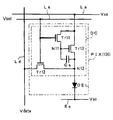
- FIG. 2 is a circuit configuration diagram illustrating an example of a pixel applied to a display panel according to an embodiment of the present invention.
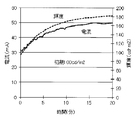
- FIG. 3 is a graph showing an actual measurement example in which the temporal transition of the organic EL current that emits light entirely from the display panel with an initial luminance of 100 cd / m 2 is observed.
- FIG. 4 is a graph showing an actual measurement example in which the temporal transition of the organic EL current that emits light from the entire surface with an initial luminance of 200 cd / m 2 is observed in the display panel.
- Figure 5 is a display panel, a graph showing measured example of observing a temporal transition of the center temperature of the display panel surface to the entire surface light emission at an initial luminance of 100cd / m 2, 200cd / m 2.
- FIG. 6 is a diagram showing an approximate polynomial used in current value prediction obtained from an actual measurement value of a cathode current value when light is emitted from the entire surface in a display panel according to an embodiment of the present invention.
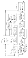
- FIG. 7 is a diagram illustrating a circuit configuration of a controller according to an embodiment of the present invention.
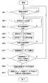
- FIG. 8 is a flowchart showing an average predicted current value calculation process according to an embodiment of the present invention.
- FIG. 9 is a flowchart showing an average cathode current value calculation process according to an embodiment of the present invention.
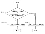
- FIG. 10 is a flowchart showing a driver transfer data calculation process according to an embodiment of the present invention.
- FIG. 11 is a verification result (transition of display panel surface temperature) in one embodiment of the present invention.
- FIG. 12 is a verification result (luminance transition) in an embodiment of the present invention.
- FIG. 13 is a verification result (current transition) in one embodiment of the present invention.
- FIG. 1 is a schematic configuration diagram showing a display device to which a display control device according to an embodiment of the present invention is applied.
- a display device (light emitting device) 100 schematically includes a display panel (light emitting panel) 101, a scan driver 102, a power driver 103, a data driver 104, and a controller 105. It is equipped with.
- the display panel 101 has a plurality of two-dimensional arrays (for example, p rows ⁇ q columns; p and q are positive integers) in the scanning direction (up and down direction in the drawing) and the column direction (left and right direction in the drawing).
- the electrode Ec and a plurality of data lines Ld arranged so as to be connected to the pixels PIX106 arranged in the column direction.
- the current flowing through the common electrode Ec is hereinafter referred to as a cathode current for convenience.
- the controller 105 has a function of performing current-voltage conversion on the common electrode Ec and converting the analog value into a digital value, and performs control using the cathode current in the present invention.
- the pixels PIX 106 arranged on the display panel 101 include a current-driven light-emitting element and a light-emitting drive circuit that generates a current for driving the light-emitting element to emit light.
- the scanning driver 102 is connected to each scanning line Ls arranged in the scanning direction of the display panel 101 described above.
- the scanning driver 102 sequentially applies a scanning signal Ssel of a predetermined voltage level (scanning level or non-scanning level) to each scanning line Ls at a predetermined timing based on a scanning control signal supplied from a controller 105 described later.
- a scanning signal Ssel of a predetermined voltage level (scanning level or non-scanning level)
- a scanning driver 102 for example, a configuration including a shift register and an output circuit is applied.
- the shift register sequentially outputs a shift signal corresponding to each scanning line Ls based on a scanning control signal (scanning clock signal, scanning start signal) supplied from the controller 105.
- the output circuit converts the shift signal from the shift register into a predetermined signal level (scanning level; for example, high level), and outputs to each scanning line Ls based on the scanning control signal (output enable signal) supplied from the controller 105. It outputs sequentially as scanning signal Ssel.
- the output order (shift direction) of the shift signals in the shift register is forward or reverse based on the scan control signal (shift switching signal) supplied from the controller 105. It is configured to be controlled to switch in the direction. Accordingly, the scanning driver 102 sequentially outputs the scanning signal Ssel from the first scanning line Ls of the display panel 101 in the forward direction in the direction of the last scanning line Ls, and the last scanning line Ls. The scanning direction is switched to the state of sequentially outputting in the direction opposite to the scanning line Ls direction of the first row. Note that specific output control of the scanning signal Ssel in the scanning driver 102 will be described later.
- the power supply driver 103 is connected to each power supply line La arranged in the scanning direction of the display panel 101. Based on a power control signal (for example, an output control signal) supplied from a controller 105 described later, the power driver 103 applies a predetermined voltage level (light emission level and non-light emission level) to the power line La for each scan at a predetermined timing. A power supply voltage Vsa is applied.
- the data driver 104 is connected to a plurality of data lines Ld arranged on the display panel 101, and each data driver 104 is driven based on a data driver control signal supplied from a controller 105 described later, and at least a display operation ( In the light emission operation), a gradation signal (gradation voltage Vdata) corresponding to the image data is generated and supplied to the pixels PIX 106 simultaneously through the data lines Ld.
- a gradation signal (gradation voltage Vdata) corresponding to the image data is generated and supplied to the pixels PIX 106 simultaneously through the data lines Ld.
- FIG. 2 is a configuration diagram illustrating an example of the pixel PIX 106 applied to the display panel 101 according to the present embodiment.
- a configuration of a pixel corresponding to an active matrix driving method is shown, and a case where an organic EL element OEL is applied as a light emitting element will be described.
- each pixel PIX 106 applied to the display panel 101 is near each intersection of the scanning line Ls connected to the scanning driver 102 and the data line Ld connected to the data driver 104.
- Each pixel PIX 106 includes an organic EL element OEL, which is a current-driven light emitting element, and a light emission drive circuit DC that generates a current for driving the organic EL element OEL to emit light.
- the light emission drive circuit DC shown in FIG. 2 generally has a circuit configuration including transistors Tr11 to Tr13 and a capacitor Cs.
- the transistor Tr11 has a gate terminal connected to the scanning line Ls, a drain terminal connected to the power supply line La, and a source terminal connected to the contact N11.
- the transistor Tr12 has a gate terminal connected to the scanning line Ls, a source terminal connected to the data line Ld, and a drain terminal connected to the contact N12.
- the transistor (drive control element) Tr13 has a gate terminal connected to the contact N11, a drain terminal connected to the power supply line La, and a source terminal connected to the contact N12.
- the capacitor (capacitance element) Cs is connected between the gate terminal (contact N11) and the source terminal (contact N12) of the transistor Tr13.
- the capacitor Cs may be a parasitic capacitance formed between the gate and the source terminal of the transistor Tr13, or in addition to the parasitic capacitance, a separate capacitive element is connected in parallel between the contact N11 and the contact N12. It may be.
- the organic EL element OEL has an anode (anode electrode) connected to the contact N12 of the light emission drive circuit DC and a cathode (cathode electrode) connected to the common electrode Ec.
- the common electrode Ec is connected to a constant voltage source (not shown), and a predetermined reference voltage Vsc (for example, ground potential GND) is applied.
- the transistors Tr11 to Tr13 for example, thin film transistors (TFTs) having the same channel type can be applied.
- the transistors Tr11 to Tr13 may be amorphous silicon thin film transistors or polysilicon thin film transistors.
- the transistors Tr11 to Tr13 are polysilicon thin film transistors
- the transistors Tr11 to Tr13 may be p-channel thin film transistors. In this case, in the configuration of the light emission drive circuit DC, the source terminals and drain terminals of the transistors Tr11 to Tr13 are reversed.
- the present invention is not limited to this embodiment, and the light emission drive circuit DC may have another circuit configuration including three or more transistors.
- the scan driver 102 applies a scan voltage (for example, a high level) scan voltage Vsel to the scan line Ls of a specific row in the scan period.
- the power supply driver 103 applies a power supply voltage Vsa of a non-light emission level (voltage level equal to or lower than the reference voltage Vsc; for example, a negative voltage) to the power supply line La of the scanning line Ls.
- the transistors Tr11 and Tr12 of each pixel PIX106 are turned on, and the pixels PIX106 in the row are set in the scanning state.
- the gradation voltage Vdata having a negative voltage value corresponding to the image data is applied from the data driver 104 to the data line Ld of each column, whereby the potential corresponding to the gradation voltage Vdata is changed to each pixel. Applied to the contact N12 of the PIX 106.
- the transistor Tr13 of each pixel PIX106 is turned on, and the write current corresponding to the potential difference generated between the gate and the source of the transistor Tr13 is transferred from the power supply line La through the transistor Tr13, the contact N12, and the transistor Tr12. It flows in the direction of the line Ld. At this time, charges corresponding to the potential difference generated between the contacts N11 and N12 are accumulated in the capacitor Cs of each pixel PIX106.
- the power supply line La is set so that a power supply voltage Vsa equal to or lower than the reference voltage Vsc is applied and the write current is drawn from the pixel PIX 106 in the direction of the data line Ld.
- Vsa the potential applied to the anode (contact N12) of the organic EL element OEL is lower than the cathode potential (reference voltage Vsc). Therefore, no current flows through the organic EL element OEL, and the organic EL element OEL Does not emit light (non-emission operation). Then, such a writing operation is sequentially executed for the pixels PIX106 of all the scanning lines that are two-dimensionally arranged on the display panel 101.
- the power supply driver 103 applies a power supply voltage Vsa having a light emission level (a voltage level higher than the reference voltage Vsc) to the power supply line La, whereby the organic EL element OEL is supplied from the power supply line La through the transistor Tr13 and the contact N12. A predetermined light emission drive current flows.
- the electric charge (voltage component) accumulated in the capacitor Cs of each pixel PIX106 corresponds to a potential difference when a write current corresponding to the gradation voltage Vdata is caused to flow in the transistor Tr13, and thus light emission flowing through the organic EL element OEL.
- the drive current has a current value substantially equal to the write current.
- the organic EL element OEL of each pixel PIX emits light with a luminance gradation corresponding to the image data (gradation voltage Vdata) written during the writing operation, and desired image information is displayed on the display panel 101. .
- FIGS. 3 and 4 the display panel 101 having pixels PIX106 described above, the initial luminance 100 cd / m 2, at 200 cd / m 2 of the common electrode Ec of the continuous emission of the pixel data to fully light emission current and luminance, respectively It is a graph which shows the example of measurement which observed temporal transition.
- FIG. 5 is a graph showing the center temperature of the surface of the display panel 101 at that time. In a continuous light emission state, all shift to an equilibrium state with time, but the organic EL element OEL has a tendency that the light emission luminance increases as the temperature rises. When viewed as a display, it does not appear as a desired display from the input image data.
- the temperature rise is close to 100 ° C., causing deterioration in the organic EL element OEL itself, which becomes a factor for shortening the lifetime of the organic EL element OEL.
- the average current value of all the pixels predicted to be necessary for the original display is obtained from the image data input for a plurality of screens (a plurality of frames), and the actual By calculating the average current value for the same screen from the measured current value when the image is displayed on the screen and comparing the two, the brightness of the display image is controlled to prevent an excessive temperature rise.
- FIG. 6 shows the display panel 101 used in FIG. 3, FIG. 4, and FIG. 5 described above, with respect to input data of gradation values (pixel values) 100 to 255 (2 to the 8th power) at an environmental temperature of 25 ° C. It is a figure which calculates
- a heat sink with a large heat capacity is placed in contact with both sides of the display panel 101 so that the temperature rise due to light emission is not affected, and the cathode current is measured by confirming that the center temperature of the display section does not rise. To do.
- the input data (gradation value) is set to 100 or more in the 256 gradations is that stress on the display panel 101 is large and a certain amount of light emission is assumed. is not.
- the digital value of the cathode current obtained by this approximate polynomial is used as the predicted current value.
- the approximate polynomial is calculated from the measured value of the cathode current. However, it may be obtained from the transistor characteristics, the light emission efficiency of the organic EL element, and the display panel pixel size.
- FIG. 7 is a diagram showing a circuit configuration of the controller 105 according to an embodiment of the present invention.
- FIG. 8 is a flowchart showing an average predicted current value calculation process according to an embodiment of the present invention, and calculates the average of the image data of all pixels from input image data (gradation values indicating shading) for a plurality of screens. The flowchart to calculate is shown.
- FIG. 9 is a flowchart showing an average cathode current value calculation process according to an embodiment of the present invention, and shows a flowchart for calculating an average current value for the plurality of screens actually displayed.
- FIG. 10 is a flowchart showing the processing for calculating the driver transfer data according to an embodiment of the present invention. The results calculated by the flowcharts shown in FIGS. 8 and 9 are compared and transferred from the controller 105 to the data driver 104.
- 5 is a flowchart for controlling brightness by calculating light emission image data.
- step S802 the input image data (gradation value) is added in the column direction by the data addition module 701.
- the division module 702 divides the total addition data in one column direction by the number of pixels in the column direction.
- the data addition module 703 adds the result calculated in S804 in the scanning direction.
- the division module 702 divides the result of the data addition module 703 by the number of pixels in the scanning direction. That is, the division result is an average of all pixels of input data for one screen.
- the result calculated in S807 is added by the data addition module 704, and it is determined whether data for any n screens has been added. If not reached, the process returns to S801 to wait for the vertical synchronization signal. If it has reached, the result obtained by adding all the pixel averages of the input data for one screen for n screens is stored in the data addition module 704.
- the division module 705 divides the data stored in the data addition module 704 by n. That is, this result is a pixel average of input data for n screens.
- the data addition module 701, the division module 702, the data addition module 703, the data addition module 704, and the division module 705 constitute an arithmetic circuit that calculates the average of all the pixels of the input data (image data).
- the current prediction module 706 performs an operation according to the approximate polynomial (see FIG. 6) based on the result calculated by the division module 705, and is necessary for the original display from the all pixel average data.
- the current value to be calculated is calculated (predicting the required current value). This necessary current value is digitally converted.
- the current prediction module 706 is an arithmetic circuit that calculates a predicted value of the current flowing through the common electrode Ec of the display panel 101 from the average of the input data (image data).
- the cathode current flowing through the common electrode Ec is converted into a voltage value according to the cathode current by a current-voltage converter 707 in the controller 105 and is converted into digital data by an ADC (Analog Digital Converter) 708.
- ADC Analog Digital Converter
- step S904 the division module 710 divides the cathode current value by n. That is, this result is an actual cathode current average value for n screens.
- the current-voltage converter 707, the ADC 708, the data addition module 709, and the division module 710 correspond to an arithmetic circuit that obtains an actual measurement value of the current flowing through the common electrode Ec when the light emitting element emits light.
- the current value (predicted value of the current flowing through the common electrode Ec) that should be necessary for the original display calculated in the process of S810 from the average data of all pixels for n screens, and the process of S904
- a comparison operation module 711 that is an operation circuit that compares the calculated cathode current average value for n screens (actual measurement value of the current flowing through the common electrode Ec) with each other is compared.
- the cathode current average value for n screens is larger than the current value that should be required for the original display calculated from the average data for all pixels for n screens, the process proceeds to S102. Proceed to the process.
- the average value of the cathode current that is actually flowing (average of the actual measurement values) is larger than the current value that is predicted to be necessary for the original display.
- the driver transfer data calculation module 712 corresponding to the correction circuit that corrects the gradation signal according to the image data inputs the input data for n screens stored in the frame memory 713 for n screens, and To perform arithmetic processing. Specifically, the driver transfer data calculation module 712 corrects the gradation value of the input data so that the brightness of the organic EL element OEL is lower than when the controller 105 transfers the input data to the data driver 104 as it is. Forward (decrease).
- the driver transfer data calculation module 712 is n Input data for n screens stored in the screen frame memory 713 is input, and arithmetic processing is performed on the data. Specifically, the driver transfer data calculation module 712 corrects the gradation value of the input data so that the brightness of the organic EL element OEL is higher than when the controller 105 transfers the input data to the data driver 104 as it is. Forward (increase).
- FIG. 11 shows the center temperature of the display unit
- FIG. 12 shows the luminance
- FIG. 13 shows the temporal transition of the cathode current.
- the environmental temperature is 28 ° C.
- the display panel 101 is not subjected to heat countermeasures such as a heat sink, and is only radiated by natural convection.
- the input data was the same data for all pixels, and the initial luminance was 170 cd / m 2 , 370 cd / m 2 , and 775 cd / m 2 . All the results suppress excessive increase, and have a remarkable effect on the target temperature increase suppression.
- the present invention can be used in a display control device or the like that can suppress a rise in the temperature of the display panel by controlling the value of the current flowing through the pixel circuit and suppress a change in image quality.
Landscapes
- Engineering & Computer Science (AREA)
- Microelectronics & Electronic Packaging (AREA)
- Physics & Mathematics (AREA)
- Computer Hardware Design (AREA)
- General Physics & Mathematics (AREA)
- Theoretical Computer Science (AREA)
- Electroluminescent Light Sources (AREA)
- Control Of Indicators Other Than Cathode Ray Tubes (AREA)
- Control Of El Displays (AREA)
Abstract
画素回路に流す電流値を制御することで表示パネルの温度上昇を抑制し、画質の変化を抑えることができる表示制御装置を提供する。 各々が発光素子を有する複数の画素が2次元配列された発光パネルに対して、画像データに応じた階調信号を供給し、発光パネルに画像情報を表示させる表示制御装置は、画像データの平均を求める演算回路と、画像データの平均から発光パネルの共通電極に流れる電流の予測値を求める演算回路と、発光素子が発光したときに共通電極に流れる電流の実測値を求める演算回路と、予測値と実測値を比較する演算回路と、比較結果に応じて画像データに応じた階調信号を補正する補正回路とを備える。
Description
本発明は、表示制御装置に関し、より詳しくは、画素回路に流す電流値を制御することで表示パネルの温度上昇を抑制し、画質の変化を抑えることができる表示制御装置に関する。
近年、液晶表示装置に続く次世代の表示デバイスとして、発光素子をマトリクス状に配列した表示パネル(画素アレイ)を備えた発光素子型の表示装置(発光装置)が注目されている。このような発光素子としては、例えば有機エレクトロルミネッセンス素子(有機EL素子)や無機エレクトロルミネッセンス素子(無機EL素子)、発光ダイオード(LED)等のような電流駆動型の発光素子が知られている。
特に、アクティブマトリクス型の駆動方式を適用した発光素子型の表示装置においては、周知の液晶表示装置に比較して、表示応答速度が速く、また、視野角依存性もほとんどなく、高輝度・高コントラスト化、表示画質の高精細化等が可能であるという優れた表示特性を有している。また、発光素子型の表示装置は、液晶表示装置のようにバックライトや導光板を必要としないので、一層の薄型軽量化が可能であるという極めて優位な特徴を有している。そのため、今後様々な電子機器への適用が期待されている。
このような発光素子型の表示装置として、例えば、特許文献1に記載されたような有機ELディスプレイ装置が知られている。この有機ELディスプレイ装置は、電圧信号によって電流制御されるアクティブマトリクス駆動表示装置であって、画像データに応じた電圧信号がゲートに印加されて、発光素子としての有機EL素子に電流を流す電流制御用薄膜トランジスタと、この電流制御用薄膜トランジスタのゲートに画像データに応じた電圧信号を供給するためのスイッチングを行うスイッチ用薄膜トランジスタとを有する回路(便宜的に、「画素回路」と記す)が、画素ごとに設けられている。また、表示映像データと電源容量から1画面に点灯している水平走査線数(点灯率)を制御することで、明るさを制御するようにしている。
しかし、有機ELディスプレイ装置のような発光素子は、環境温度および自らの発光による発熱に伴い表示パネル温度が上昇することで、画素回路に流れる電流値が本来の表示に必要な電流値よりも上昇してしまい、その結果発光輝度が高くなる傾向がある。そのため、同じ表示映像データであっても表示パネルの温度によって画質が変化してしまうという問題がある。また、電流値の上昇により表示パネル温度が上昇し、その結果、さらに電流値が上昇するという悪循環も生じてしまう。
本発明は、上述した課題においてなされたものであって、画素回路に流す電流値を制御することで表示パネルの温度上昇を抑制し、画質の変化を抑えることができる表示制御装置を提供することを目的とする。
上記課題を解決するための本発明の一局面は、各々が発光素子を有する複数の画素が2次元配列された発光パネルに対して、画像データに応じた階調信号を供給し、発光パネルに画像情報を表示させる表示制御装置において、画像データの平均を求める演算回路と、画像データの平均から発光パネルの共通電極に流れる電流の予測値を求める演算回路と、発光素子が発光したときに共通電極に流れる電流の実測値を求める演算回路と、予測値と実測値とを比較する演算回路と、予測値と実測値との比較結果に応じて、画像データに応じた階調信号を補正する補正回路とを備える、表示制御装置である。
本発明に係る表示制御装置によれば、発光による表示パネル温度上昇による所望の輝度以上での発光を抑制でき、また発光による過剰な温度上昇を防止できる。すなわち、画素回路に流す電流値を制御することで表示パネルの温度上昇を抑制し、画質の変化を抑えることができる表示制御装置を提供することができる。
以下、本発明の実施形態に係る、表示パネルの表示制御装置について、実施形態を示して、詳しく説明する。
図1は、本発明の一実施形態に係る表示制御装置を適用した表示装置を示す概略構成図である。図1に示すように、本実施形態に係る表示装置(発光装置)100は、概略、表示パネル(発光パネル)101と、走査ドライバ102と、電源ドライバ103と、データドライバ104と、コントローラ105と、を備えている。
表示パネル101は、図1に示すように、走査方向(図面上下方向)及び列方向(図面左右方向)に2次元配列(例えばp行×q列;p、qは正の整数)された複数の画素PIX106と、各々走査方向(行方向)に配列された画素PIX106に接続するように配設された複数の走査ラインLs及び複数の電源ラインLaと、全画素PIX106に共通に設けられた共通電極Ecと、列方向に配列された画素PIX106に接続するように配設された複数のデータラインLdと、を有している。ここで、共通電極Ecを流れる電流を便宜的に以降、カソード電流と呼ぶ。コントローラ105には、共通電極Ecに対して電流電圧変換を行い、そのアナログ値をデジタル値に変換する機能を有し、本発明におけるカソード電流を利用した制御を実施する。
また、表示パネル101に配列された画素PIX106は、後述するように、電流駆動型の発光素子と、発光素子を発光駆動するための電流を生成する発光駆動回路と、を備えている。
走査ドライバ102は、上記の表示パネル101の走査方向に配設された各走査ラインLsに接続されている。走査ドライバ102は、後述するコントローラ105から供給される走査制御信号に基づいて、各走査ラインLsに所定のタイミングで所定の電圧レベル(走査レベル又は非走査レベル)の走査信号Sselを順次印加することにより、各走査の画素PIX106を順次走査状態に設定する。
このような走査ドライバ102としては、例えば、シフトレジスタと出力回路とを備えた構成が適用される。シフトレジスタは、コントローラ105から供給される走査制御信号(走査クロック信号、走査スタート信号)に基づいて、各走査ラインLsに対応するシフト信号を順次出力する。出力回路は、シフトレジスタからのシフト信号を所定の信号レベル(走査レベル;例えばハイレベル)に変換し、コントローラ105から供給される走査制御信号(出力イネーブル信号)に基づいて、各走査ラインLsに走査信号Sselとして順次出力する。
さらに、本実施形態に適用される走査ドライバ102においては、コントローラ105から供給される走査制御信号(シフト切替信号)に基づいて、シフトレジスタにおけるシフト信号の出力順序(シフト方向)が順方向又は逆方向に切り替え制御されるように構成されている。これにより、走査ドライバ102は、走査信号Sselを、表示パネル101の1行目の走査ラインLsから最終行目の走査ラインLs方向の順方向に順次出力する状態と、最終行目の走査ラインLsから1行目の走査ラインLs方向の逆方向に順次出力する状態とに、走査方向が切り替え設定される。なお、走査ドライバ102における走査信号Sselの具体的な出力制御については後述する。
電源ドライバ103は、表示パネル101の走査方向に配設された各電源ラインLaに接続されている。電源ドライバ103は、後述するコントローラ105から供給される電源制御信号(例えば出力制御信号)に基づいて、各走査の電源ラインLaに所定のタイミングで所定の電圧レベル(発光レベル及び非発光レベル)の電源電圧Vsaを印加する。
データドライバ104は、表示パネル101に配設された複数のデータラインLdに接続され、各データドライバ104は、後述するコントローラ105から供給されるデータドライバ制御信号に基づいて駆動され、少なくとも表示動作(発光動作)時に、画像データに応じた階調信号(階調電圧Vdata)を生成して、各データラインLdを介して画素PIX106へ一斉に供給する。
図2は、本実施形態に係る表示パネル101に適用される画素PIX106の一例を示す構成図である。ここでは、アクティブマトリクス型の駆動方式に対応した画素の構成を示し、また、発光素子として有機EL素子OELを適用した場合について説明する。
本実施形態に係る表示パネル101に適用される画素PIX106は、図2に示すように、走査ドライバ102に接続された走査ラインLsとデータドライバ104に接続されたデータラインLdとの各交点近傍に配置されている。各画素PIX106は、電流駆動型の発光素子である有機EL素子OELと、有機EL素子OELを発光駆動するための電流を生成する発光駆動回路DCと、を備えている。
図2に示す発光駆動回路DCは、概略、トランジスタTr11~Tr13と、キャパシタCsと、を備えた回路構成を有している。トランジスタTr11は、ゲート端子が走査ラインLsに接続され、また、ドレイン端子が電源ラインLaに接続され、また、ソース端子が接点N11に接続されている。トランジスタTr12は、ゲート端子が走査ラインLsに接続され、また、ソース端子がデータラインLdに接続され、また、ドレイン端子が接点N12に接続されている。トランジスタ(駆動制御素子)Tr13は、ゲート端子が接点N11に接続され、ドレイン端子が電源ラインLaに接続され、ソース端子が接点N12に接続されている。また、キャパシタ(容量素子)Csは、トランジスタTr13のゲート端子(接点N11)及びソース端子(接点N12)間に接続されている。ここで、キャパシタCsは、トランジスタTr13のゲート・ソース端子間に形成される寄生容量であってもよいし、寄生容量に加えて接点N11及び接点N12間に別個の容量素子を並列に接続したものであってもよい。
また、有機EL素子OELは、アノード(アノード電極)が上記発光駆動回路DCの接点N12に接続され、カソード(カソード電極)が共通電極Ecに接続されている。共通電極Ecは、図示を省略した定電圧源に接続され、所定の基準電圧Vsc(例えば接地電位GND)が印加されている。
なお、図2に示した画素PIX106において、トランジスタTr11~Tr13については、例えば同一のチャネル型を有する薄膜トランジスタ(TFT)を適用することができる。トランジスタTr11~Tr13は、アモルファスシリコン薄膜トランジスタであってもよいし、ポリシリコン薄膜トランジスタであってもよい。
特に、図2に示すように、トランジスタTr11~Tr13として、例えばnチャネル型の薄膜トランジスタを適用し、かつ、トランジスタTr11~Tr13としてアモルファスシリコン薄膜トランジスタを適用した場合には、すでに確立されたアモルファスシリコン製造技術を適用して、多結晶型や単結晶型のシリコン薄膜トランジスタに比較して、簡易な製造プロセスで動作特性(電子移動度等)が均一で安定したトランジスタを実現することができる。
また、トランジスタTr11~Tr13がポリシリコン薄膜トランジスタである場合、トランジスタTr11~Tr13はpチャネル型の薄膜トランジスタであってもよい。この場合には発光駆動回路DCの構成において、各トランジスタTr11~Tr13のソース端子とドレイン端子とが逆になる。
また、上述した画素PIX106においては、発光駆動回路DCとして3個のトランジスタTr11~Tr13を備えた回路構成を示した。本発明はこの実施形態に限定されるものではなく、発光駆動回路DCが3個以上のトランジスタを備えた他の回路構成を有するものであってもよい。
次いで、このような回路構成を有する画素PIX106を備えた表示装置の表示動作について、簡単に説明する。図2に示した画素PIX106を備えた表示装置の表示動作は、まず、走査期間において、走査ドライバ102から特定の行の走査ラインLsに走査レベル(例えばハイレベル)の走査電圧Vselを印加するとともに、電源ドライバ103から当該走査ラインLsの電源ラインLaに非発光レベル(基準電圧Vsc以下の電圧レベル;例えば負電圧)の電源電圧Vsaを印加する。これにより、各画素PIX106のトランジスタTr11、Tr12がオン動作して、当該行の画素PIX106が走査状態に設定される。このタイミングに同期して、画像データに応じた負の電圧値の階調電圧Vdataを、データドライバ104から各列のデータラインLdに印加することにより、階調電圧Vdataに応じた電位が各画素PIX106の接点N12に印加される。
これにより、各画素PIX106のトランジスタTr13がオン動作して、トランジスタTr13のゲート・ソース間に生じた電位差に応じた書込電流が、電源ラインLaからトランジスタTr13、接点N12、トランジスタTr12を介してデータラインLd方向に流れる。このとき、各画素PIX106のキャパシタCsには、接点N11及びN12間に生じた電位差に応じた電荷が蓄積される。
ここで、電源ラインLaには、基準電圧Vsc以下の電源電圧Vsaが印加され、さらに、書込電流が画素PIX106からデータラインLd方向に引き抜かれるように設定されている。これにより、有機EL素子OELのアノード(接点N12)に印加される電位は、カソードの電位(基準電圧Vsc)よりも低くなるため、有機EL素子OELには電流が流れず、有機EL素子OELは発光しない(非発光動作)。そして、このような書込動作を、表示パネル101に2次元配列された全ての走査ラインの画素PIX106について順次実行する。
次いで、非走査期間において、走査ドライバ102から走査ラインLsに非走査レベル(例えばローレベル)の走査電圧Vselを印加することにより、各画素PIX106のトランジスタTr11、Tr12がオフ動作して、当該行の画素PIX106が非走査状態に設定される。これにより、各画素PIX106のキャパシタCsに走査期間において蓄積された電荷が保持されるので、トランジスタTr13はオン状態を維持する。そして、電源ドライバ103から電源ラインLaに発光レベル(基準電圧Vscよりも高い電圧レベル)の電源電圧Vsaを印加することにより、電源ラインLaからトランジスタTr13、接点N12を介して、有機EL素子OELに所定の発光駆動電流が流れる。
このとき、各画素PIX106のキャパシタCsに蓄積される電荷(電圧成分)は、トランジスタTr13において階調電圧Vdataに対応する書込電流を流す場合の電位差に相当するので、有機EL素子OELに流れる発光駆動電流は、書込電流と略同等の電流値となる。これにより、各画素PIXの有機EL素子OELは、書込動作時に書き込まれた画像データ(階調電圧Vdata)に応じた輝度階調で発光し、表示パネル101に所望の画像情報が表示される。
図3・図4は、前述した画素PIX106を有する表示パネル101において、それぞれ初期輝度100cd/m2、200cd/m2で全面発光する画素データでの連続発光時の共通電極Ecの電流及び輝度の時間的推移を観測した実測例を示すグラフである。また図5は、その時の表示パネル101表面の中心温度を示すグラフである。連続した発光状態で、いずれも時間とともに平衡状態に移行していくが、有機EL素子OELは、温度上昇に伴い発光輝度が高くなる傾向を有している。ディスプレイとしてみたときに、入力された画像データからの所望の表示とは見えない。初期輝度200cd/m2においては、温度上昇が100℃近くあり、有機EL素子OEL自身に劣化を生じさせ、有機EL素子OELの寿命を短くする要因ともなってしまう。
そこで本発明では、共通電極Ecを流れる電流について、複数画面(複数フレーム)分の入力される画像データから、本来の表示に必要であると予測される全画素の平均電流値を求めるとともに、実際に画像を表示しているときの電流実測値から同画面分の平均電流値を求めて、両者を比較することにより、表示画像の明るさを制御し、過度の温度上昇を防止する。
図6は、前述の図3、図4、図5で使用した表示パネル101において、環境温度が25℃で階調値(画素値)100~255(2の8乗)の入力データに対し、全面発光させたときのカソード電流の実測値から、後述する電流値予測で用いられる近似多項式を求めて示す図である。近似多項式を求める際、発光による温度上昇が影響することのないよう、表示パネル101には熱容量の大きな放熱ヒートシンクを両面に接触配置し表示部中心温度が上昇しないことを確認してカソード電流を実測する。入力データ(階調値)を256階調の中で100以上としたのは、表示パネル101へのストレスが大きい、ある程度の発光を想定したためであり、実使用環境等において、これに限定するものではない。そして、この近似多項式で求められるカソード電流のデジタル値を、予測される電流値として使用する。また、本例では近似多項式をカソード電流の実測値から算出したが、トランジスタ特性、有機EL素子の発光効率、表示パネル画素サイズから求めてもよい。
図7は、本発明の一実施形態に係るコントローラ105の回路構成を示す図である。図8は、本発明の一実施形態に係る平均予測電流値算出処理を示すフローチャートであり、複数画面分の入力される画像データ(濃淡を示す階調値)から全画素の画像データの平均を算出するフローチャートを示す。図9は、本発明の一実施形態に係る平均カソード電流値算出処理を示すフローチャートであり、実際の表示している前述複数画面分の平均電流値を算出するフローチャートを示す。図10は、本発明の一実施形態に係るドライバ転送データの演算処理を示すフローチャートであり、図8・図9に示したフローチャートによって算出した結果を比較して、コントローラ105からデータドライバ104へ転送する発光画像データを演算して明るさを制御するフローチャートを示す。
次に、図7に示した回路構成による制御方法を図8、図9、図10に基づいて説明する。
まずS801において、図7にて図示していないが垂直同期信号の入力に基づいてデータ加算モジュール701への入力が開始される。
まずS801において、図7にて図示していないが垂直同期信号の入力に基づいてデータ加算モジュール701への入力が開始される。
次にS802において、入力された画像データ(階調値)を、データ加算モジュール701にて列方向に加算していく。
次にS803において、表示パネル101の1走査の列方向画素数分、すなわち列方向画素の全データが加算されたかを判断し、到達していなければS802に戻る。
次にS804において、1走査の列方向の全加算データに対し除算モジュール702にて列方向画素数で除算する。
次にS805において、S804で算出された結果を、データ加算モジュール703にて走査方向に加算する。
次にS806において表示パネル101の走査方向画素数分、データ加算モジュール703にて加算がなされたかを判断し、到達していなければS802に戻る。到達していれば表示パネル101の1走査の列方向の画素平均値が全走査分、データ加算モジュール703にて加算されている。
次にS807においてデータ加算モジュール703の結果に対して、除算モジュール702にて走査方向画素数で除算する。すなわち、除算結果は1画面分の入力データの全画素平均となる。
次にS808においてS807で算出された結果をデータ加算モジュール704にて加算し、任意のn画面分データが加算されたかを判断し、到達していなければS801に戻り、垂直同期信号を待つ。到達していれば、1画面分の入力データの全画素平均がn画面分加算された結果が、データ加算モジュール704に格納されている。
次にS809において除算モジュール705にてデータ加算モジュール704に格納されているデータをnで除算する。すなわち、この結果はn画面分の入力データの画素平均となる。このように、データ加算モジュール701、除算モジュール702、データ加算モジュール703、データ加算モジュール704、除算モジュール705は、入力データ(画像データ)の全画素の平均を求める演算回路を構成する。
次にS810において、除算モジュール705にて算出された結果に基づいて電流予測モジュール706にて近似多項式(図6参照)に従った演算を行って、全画素平均データから本来の表示に必要とされるべき電流値を算出する(必要電流値の予測)。この必要電流値は、デジタル変換されたものとなる。このように、電流予測モジュール706は、入力データ(画像データ)の平均から表示パネル101の共通電極Ecに流れる電流の予測値を求める演算回路である。
続いて図9に示すフローチャートに従って説明する。
まず、共通電極Ecを流れるカソード電流はコントローラ105内の電流電圧変換器707にてカソード電流に従った電圧値に変換されてADC(Analog Degital Converter)708によってデジタルデータとしてある。
まず、共通電極Ecを流れるカソード電流はコントローラ105内の電流電圧変換器707にてカソード電流に従った電圧値に変換されてADC(Analog Degital Converter)708によってデジタルデータとしてある。
次にS901において垂直同期信号の入力に基づいて処理が開始される。
次にS902においてデータ加算モジュール709にてデジタル変換されたカソード電流値が各画面について加算される。
次にS903においてデータ加算モジュール709にて加算されたカソード電流値がn画面分加算されたかを判断し、到達していなければS901に戻る。到達していれば、n画面分のカソード電流値が加算された結果がデータ加算モジュール709に格納されている。
次にS904において除算モジュール710にてカソード電流値をnで除算する。
すなわち、この結果が実際のn画面分のカソード電流平均値となる。このように、電流電圧変換器707、ADC708、データ加算モジュール709、除算モジュール710は、発光素子が発光したときに共通電極Ecに流れる電流の実測値を求める演算回路に対応する。
すなわち、この結果が実際のn画面分のカソード電流平均値となる。このように、電流電圧変換器707、ADC708、データ加算モジュール709、除算モジュール710は、発光素子が発光したときに共通電極Ecに流れる電流の実測値を求める演算回路に対応する。
続いて図10に従って説明する。
まずS101において、n画面分の全画素平均データからS810の処理にて算出された本来の表示に必要とされるべき電流値(共通電極Ecに流れる電流の予測値)と、S904の処理にて算出されたn画面分のカソード電流平均値(共通電極Ecに流れる電流の実測値)とを比較する演算回路である比較演算モジュール711にて比較する。n画面分のカソード電流平均値が、n画面分の全画素平均データから算出された本来の表示に必要とされるべき電流値よりも大きい場合はS102の処理に進み、逆に小さい場合はS103の処理に進む。
まずS101において、n画面分の全画素平均データからS810の処理にて算出された本来の表示に必要とされるべき電流値(共通電極Ecに流れる電流の予測値)と、S904の処理にて算出されたn画面分のカソード電流平均値(共通電極Ecに流れる電流の実測値)とを比較する演算回路である比較演算モジュール711にて比較する。n画面分のカソード電流平均値が、n画面分の全画素平均データから算出された本来の表示に必要とされるべき電流値よりも大きい場合はS102の処理に進み、逆に小さい場合はS103の処理に進む。
次にS102の処理において、実際に流れているカソード電流の平均値(実測値の平均)が、本来の表示に必要であると予測される電流値よりも大きいので、上述の比較結果に応じて、画像データに応じた階調信号を補正する補正回路に対応するドライバ転送データ演算モジュール712は、n画面分フレームメモリ713に格納されているn画面分の入力データを入力し、そのデータに対して演算処理を行う。具体的には、コントロ-ラ105がデータドライバ104に入力データをそのまま転送する場合よりも有機EL素子OELの輝度を下げるよう、ドライバ転送データ演算モジュール712は入力データの階調値を補正して(減少させて)転送する。
S102の処理に対してS103の処理は、実際に流れているカソード電流の平均値が、本来の表示に必要であると予測される電流値よりも小さいので、ドライバ転送データ演算モジュール712は、n画面分フレームメモリ713に格納されているn画面分の入力データを入力し、そのデータに対して演算処理を行う。具体的には、コントロ-ラ105がデータドライバ104に入力データをそのまま転送する場合よりも有機EL素子OELの輝度を上げるよう、ドライバ転送データ演算モジュール712は入力データの階調値を補正して(増加させて)転送する。
図3、図4、図5の試験で使用した表示パネル101を本実施形態に係るコントローラ105を用いて制御することにより検証を行った結果を示す。図11は表示部中心温度、図12は輝度、図13はカソード電流の時間的推移である。環境温度は28℃、表示パネル101にはヒートシンク等の熱対策は実施せず、自然対流による放熱のみである。入力データは全画素同一データにて初期輝度を170cd/m2、370cd/m2、775cd/m2とした。いずれの結果も過度の上昇を抑制しており、目的である温度上昇抑制に対して顕著な効果を奏している。
本発明は、画素回路に流す電流値を制御することで表示パネルの温度上昇を抑制し、画質の変化を抑えることができる表示制御装置等に利用可能である。
100 表示装置
101 表示パネル
102 走査ドライバ
103 電源ドライバ
104 データドライバ
105 コントローラ
106 画素PIX
120 選択ドライバ
PIX 画素
DC 発光駆動回路
Tr11、Tr12、Tr13 トランジスタ
Cs キャパシタ
OEL 有機EL素子
701、703、704、709 データ加算モジュール
702、705、710 除算モジュール
706 電流予測モジュール
707 電流電圧変換器
708 ADC
711 比較演算モジュール
712 ドライバ転送データ演算モジュール
713 n画面分フレームメモリ
101 表示パネル
102 走査ドライバ
103 電源ドライバ
104 データドライバ
105 コントローラ
106 画素PIX
120 選択ドライバ
PIX 画素
DC 発光駆動回路
Tr11、Tr12、Tr13 トランジスタ
Cs キャパシタ
OEL 有機EL素子
701、703、704、709 データ加算モジュール
702、705、710 除算モジュール
706 電流予測モジュール
707 電流電圧変換器
708 ADC
711 比較演算モジュール
712 ドライバ転送データ演算モジュール
713 n画面分フレームメモリ
Claims (3)
- 各々が発光素子を有する複数の画素が2次元配列された発光パネルに対して、画像データに応じた階調信号を供給し、前記発光パネルに画像情報を表示させる表示制御装置において、
前記画像データの平均を求める演算回路と、
前記画像データの平均から前記発光パネルの共通電極に流れる電流の予測値を求める演算回路と、
前記発光素子が発光したときに前記共通電極に流れる電流の実測値を求める演算回路と、
前記予測値と前記実測値とを比較する演算回路と、
前記予測値と前記実測値との比較結果に応じて、前記画像データに応じた階調信号を補正する補正回路とを備える、表示制御装置。 - 前記予測値を求める演算回路は、連続した複数フレームを構成する画像データから全画素の画像データの平均を算出し、前記全画素の画像データの平均から前記発光パネルの共通電極に流れる電流の予測値を求める、請求項1に記載の表示制御装置。
- 前記実測値を求める演算回路は、連続した複数フレームにおいて前記共通電極に流れる電流をそれぞれ計測し、その平均電流値を求める、請求項1に記載の表示制御装置。
Applications Claiming Priority (2)
| Application Number | Priority Date | Filing Date | Title |
|---|---|---|---|
| JP2013181547A JP2015049399A (ja) | 2013-09-02 | 2013-09-02 | 表示制御装置 |
| JP2013-181547 | 2013-09-02 |
Publications (1)
| Publication Number | Publication Date |
|---|---|
| WO2015029337A1 true WO2015029337A1 (ja) | 2015-03-05 |
Family
ID=52585934
Family Applications (1)
| Application Number | Title | Priority Date | Filing Date |
|---|---|---|---|
| PCT/JP2014/004057 Ceased WO2015029337A1 (ja) | 2013-09-02 | 2014-08-04 | 表示制御装置 |
Country Status (3)
| Country | Link |
|---|---|
| JP (1) | JP2015049399A (ja) |
| TW (1) | TW201510974A (ja) |
| WO (1) | WO2015029337A1 (ja) |
Cited By (2)
| Publication number | Priority date | Publication date | Assignee | Title |
|---|---|---|---|---|
| CN106878740A (zh) * | 2015-12-10 | 2017-06-20 | 格科微电子(上海)有限公司 | 适用于液晶显示驱动的图像压缩方法和图像压缩系统 |
| CN115443498A (zh) * | 2020-05-01 | 2022-12-06 | 索尼集团公司 | 信号处理装置、信号处理方法及显示装置 |
Families Citing this family (1)
| Publication number | Priority date | Publication date | Assignee | Title |
|---|---|---|---|---|
| KR102419876B1 (ko) * | 2015-08-21 | 2022-07-12 | 삼성디스플레이 주식회사 | 열화 보상 방법 및 이를 수행하는 표시 장치 |
Citations (6)
| Publication number | Priority date | Publication date | Assignee | Title |
|---|---|---|---|---|
| JP2002311898A (ja) * | 2001-02-08 | 2002-10-25 | Semiconductor Energy Lab Co Ltd | 発光装置及びそれを用いた電子機器 |
| JP2004038209A (ja) * | 1997-03-12 | 2004-02-05 | Seiko Epson Corp | 表示装置及び電子機器 |
| JP2004271755A (ja) * | 2003-03-06 | 2004-09-30 | Kodak Kk | 有機el表示装置 |
| JP2005107059A (ja) * | 2003-09-29 | 2005-04-21 | Sanyo Electric Co Ltd | 表示装置 |
| JP2008268914A (ja) * | 2007-04-24 | 2008-11-06 | Samsung Sdi Co Ltd | 有機電界発光表示装置及びその駆動方法 |
| WO2009017156A1 (ja) * | 2007-07-30 | 2009-02-05 | Kyocera Corporation | 画像表示装置、画像表示装置の制御方法、画像表示装置の調整システム |
-
2013
- 2013-09-02 JP JP2013181547A patent/JP2015049399A/ja active Pending
-
2014
- 2014-08-04 WO PCT/JP2014/004057 patent/WO2015029337A1/ja not_active Ceased
- 2014-08-29 TW TW103129783A patent/TW201510974A/zh unknown
Patent Citations (6)
| Publication number | Priority date | Publication date | Assignee | Title |
|---|---|---|---|---|
| JP2004038209A (ja) * | 1997-03-12 | 2004-02-05 | Seiko Epson Corp | 表示装置及び電子機器 |
| JP2002311898A (ja) * | 2001-02-08 | 2002-10-25 | Semiconductor Energy Lab Co Ltd | 発光装置及びそれを用いた電子機器 |
| JP2004271755A (ja) * | 2003-03-06 | 2004-09-30 | Kodak Kk | 有機el表示装置 |
| JP2005107059A (ja) * | 2003-09-29 | 2005-04-21 | Sanyo Electric Co Ltd | 表示装置 |
| JP2008268914A (ja) * | 2007-04-24 | 2008-11-06 | Samsung Sdi Co Ltd | 有機電界発光表示装置及びその駆動方法 |
| WO2009017156A1 (ja) * | 2007-07-30 | 2009-02-05 | Kyocera Corporation | 画像表示装置、画像表示装置の制御方法、画像表示装置の調整システム |
Cited By (4)
| Publication number | Priority date | Publication date | Assignee | Title |
|---|---|---|---|---|
| CN106878740A (zh) * | 2015-12-10 | 2017-06-20 | 格科微电子(上海)有限公司 | 适用于液晶显示驱动的图像压缩方法和图像压缩系统 |
| CN106878740B (zh) * | 2015-12-10 | 2022-11-01 | 格科微电子(上海)有限公司 | 适用于液晶显示驱动的图像压缩方法和图像压缩系统 |
| CN115443498A (zh) * | 2020-05-01 | 2022-12-06 | 索尼集团公司 | 信号处理装置、信号处理方法及显示装置 |
| US12531014B2 (en) | 2020-05-01 | 2026-01-20 | Saturn Licensing Llc | Signal processing device, signal processing method, and display device |
Also Published As
| Publication number | Publication date |
|---|---|
| TW201510974A (zh) | 2015-03-16 |
| JP2015049399A (ja) | 2015-03-16 |
Similar Documents
| Publication | Publication Date | Title |
|---|---|---|
| JP5844525B2 (ja) | 画素、有機電界発光表示装置及びその駆動方法 | |
| US9646533B2 (en) | Organic light emitting display device | |
| US8872740B2 (en) | Display apparatus and display apparatus driving method | |
| US8384829B2 (en) | Display apparatus and display apparatus driving method | |
| JP5230806B2 (ja) | 画像表示装置およびその駆動方法 | |
| JP4844602B2 (ja) | 表示装置、表示制御装置、および表示制御方法、並びにプログラム | |
| JP6382923B2 (ja) | 有機発光素子表示装置およびその駆動方法 | |
| JPWO2009110132A1 (ja) | アクティブ・マトリクス型表示装置 | |
| US11373595B2 (en) | Display device and method for driving display device | |
| JP5738270B2 (ja) | 表示装置 | |
| JP7443201B2 (ja) | 表示装置及び表示装置の駆動方法 | |
| US20080246701A1 (en) | Organic light emitting display and its driving method | |
| JP4314638B2 (ja) | 表示装置及びその駆動制御方法 | |
| CN101577088B (zh) | 有机发光显示器及其驱动方法 | |
| CN102568367B (zh) | 显示装置和显示装置驱动方法 | |
| JP5399521B2 (ja) | 表示装置およびその駆動方法 | |
| WO2015029337A1 (ja) | 表示制御装置 | |
| JP2011164136A (ja) | 表示装置 | |
| JP5938742B2 (ja) | El表示装置 | |
| JP2012063733A (ja) | 有機電界発光表示装置及びその駆動方法 | |
| JP5170194B2 (ja) | 発光装置及びその駆動制御方法並びに電子機器 | |
| JP2012073367A (ja) | 発光駆動回路、発光装置及びその駆動制御方法、並びに電子機器 | |
| JP2009110007A (ja) | 表示装置の駆動方法 |
Legal Events
| Date | Code | Title | Description |
|---|---|---|---|
| 121 | Ep: the epo has been informed by wipo that ep was designated in this application |
Ref document number: 14840573 Country of ref document: EP Kind code of ref document: A1 |
|
| NENP | Non-entry into the national phase |
Ref country code: DE |
|
| 122 | Ep: pct application non-entry in european phase |
Ref document number: 14840573 Country of ref document: EP Kind code of ref document: A1 |