WO2015029294A1 - ウェーハの研磨方法およびウェーハの研磨装置 - Google Patents
ウェーハの研磨方法およびウェーハの研磨装置 Download PDFInfo
- Publication number
- WO2015029294A1 WO2015029294A1 PCT/JP2014/003393 JP2014003393W WO2015029294A1 WO 2015029294 A1 WO2015029294 A1 WO 2015029294A1 JP 2014003393 W JP2014003393 W JP 2014003393W WO 2015029294 A1 WO2015029294 A1 WO 2015029294A1
- Authority
- WO
- WIPO (PCT)
- Prior art keywords
- polishing
- wafer
- cloth
- contact angle
- polishing cloth
- Prior art date
- Legal status (The legal status is an assumption and is not a legal conclusion. Google has not performed a legal analysis and makes no representation as to the accuracy of the status listed.)
- Ceased
Links
Images


Classifications
-
- B—PERFORMING OPERATIONS; TRANSPORTING
- B24—GRINDING; POLISHING
- B24B—MACHINES, DEVICES, OR PROCESSES FOR GRINDING OR POLISHING; DRESSING OR CONDITIONING OF ABRADING SURFACES; FEEDING OF GRINDING, POLISHING, OR LAPPING AGENTS
- B24B37/00—Lapping machines or devices; Accessories
- B24B37/005—Control means for lapping machines or devices
-
- B—PERFORMING OPERATIONS; TRANSPORTING
- B24—GRINDING; POLISHING
- B24B—MACHINES, DEVICES, OR PROCESSES FOR GRINDING OR POLISHING; DRESSING OR CONDITIONING OF ABRADING SURFACES; FEEDING OF GRINDING, POLISHING, OR LAPPING AGENTS
- B24B37/00—Lapping machines or devices; Accessories
- B24B37/11—Lapping tools
- B24B37/20—Lapping pads for working plane surfaces
-
- B—PERFORMING OPERATIONS; TRANSPORTING
- B24—GRINDING; POLISHING
- B24B—MACHINES, DEVICES, OR PROCESSES FOR GRINDING OR POLISHING; DRESSING OR CONDITIONING OF ABRADING SURFACES; FEEDING OF GRINDING, POLISHING, OR LAPPING AGENTS
- B24B37/00—Lapping machines or devices; Accessories
- B24B37/34—Accessories
-
- B—PERFORMING OPERATIONS; TRANSPORTING
- B24—GRINDING; POLISHING
- B24B—MACHINES, DEVICES, OR PROCESSES FOR GRINDING OR POLISHING; DRESSING OR CONDITIONING OF ABRADING SURFACES; FEEDING OF GRINDING, POLISHING, OR LAPPING AGENTS
- B24B49/00—Measuring or gauging equipment for controlling the feed movement of the grinding tool or work; Arrangements of indicating or measuring equipment, e.g. for indicating the start of the grinding operation
- B24B49/02—Measuring or gauging equipment for controlling the feed movement of the grinding tool or work; Arrangements of indicating or measuring equipment, e.g. for indicating the start of the grinding operation according to the instantaneous size and required size of the workpiece acted upon, the measuring or gauging being continuous or intermittent
- B24B49/06—Measuring or gauging equipment for controlling the feed movement of the grinding tool or work; Arrangements of indicating or measuring equipment, e.g. for indicating the start of the grinding operation according to the instantaneous size and required size of the workpiece acted upon, the measuring or gauging being continuous or intermittent requiring comparison of the workpiece with standard gauging plugs, rings or the like
-
- H—ELECTRICITY
- H10—SEMICONDUCTOR DEVICES; ELECTRIC SOLID-STATE DEVICES NOT OTHERWISE PROVIDED FOR
- H10P—GENERIC PROCESSES OR APPARATUS FOR THE MANUFACTURE OR TREATMENT OF DEVICES COVERED BY CLASS H10
- H10P90/00—Preparation of wafers not covered by a single main group of this subclass, e.g. wafer reinforcement
- H10P90/12—Preparing bulk and homogeneous wafers
- H10P90/129—Preparing bulk and homogeneous wafers by polishing
Definitions
- the present invention relates to a wafer polishing method and a wafer polishing apparatus.
- a process for manufacturing a semiconductor wafer mainly includes a single crystal pulling process for manufacturing a single crystal ingot and a processing process for the manufactured single crystal ingot.
- This processing process generally includes a slicing process, a lapping process, a chamfering process, an etching process, a mirror polishing process, a cleaning process, and the like, and a semiconductor wafer having a mirror-finished surface is manufactured through these processes.
- a multi-stage polishing process such as rough polishing or finish polishing is performed.
- one side of the wafer is mechanochemically polished (CMP) with a single-side polishing apparatus 200 as shown in FIG.
- CMP is a polishing technique in which a polishing liquid that has an etching action on a wafer that is an object to be polished is used, and the wafer is mechanically polished with abrasive grains contained in the polishing liquid while the wafer is being etched.
- the single-side polishing apparatus 200 includes a head 202 that holds a wafer, and a surface plate 210 provided with a polishing cloth 212 on the surface.
- the head 202 presses the surface to be polished of the wafer against the polishing cloth 212. Then, the wafer surface is polished by rotating the head 202 and the surface plate 210 together while supplying the polishing liquid 228 from the polishing liquid supply unit 226 onto the polishing cloth 212.
- the number of dummy polishings is set in advance so that wafers with a large number of LPDs are not mixed in product wafers, the probability of wafer loss due to dummy polishing increases, and conversely, wafer loss due to dummy polishing increases. If the number of dummy polishings is set to be small for the purpose of reducing the number of wafers, the probability that a wafer with a large number of LPDs will be mixed in the product wafer increases.
- Patent Document 1 describes that dummy polishing is performed until the copper concentration in the polishing cloth becomes 0.01 ppm or less.
- this method requires a test piece to be cut out from the polishing cloth in order to measure the copper concentration, and there is room for improvement in practical use.
- the present invention provides a practical wafer polishing method and wafer polishing apparatus capable of reducing wafer loss due to dummy polishing and stabilizing the number of product wafer LPDs at a low level.
- the purpose is to provide.
- the present inventor studied to achieve this object, and the following knowledge was obtained. That is, the present inventor paid attention to the contact angle of the polishing cloth as an index for grasping the surface state of the polishing cloth. Then, it was found that there is a good correlation between the contact angle of the polishing cloth and the number of LPDs of the wafer polished with the polishing cloth.
- the method for polishing a wafer of the present invention comprises: A wafer polishing method in which the wafer is brought into contact with a polishing cloth provided on the surface of the surface plate, and the surface plate and the wafer are rotated to polish the surface of the wafer multiple times with the same polishing cloth. Because The polishing process includes an initial polishing step in which the wafer after polishing is not a product, and a main polishing step in which the wafer after polishing is a product after the initial polishing step, The contact angle of the polishing cloth is measured, and the switching time from the initial polishing step to the main polishing step is determined based on the measured value.
- the contact angle of the polishing cloth is measured every time or periodically before the polishing process, and the polishing process after the measurement value is stabilized can be determined as the main polishing process. .
- the subsequent polishing process can be determined as the main polishing step.
- the threshold is determined based on
- the wafer to be polished in the initial polishing step is a dummy wafer.
- the contact angle of the polishing cloth is measured again, and the replacement timing of the polishing cloth in the main polishing step is determined based on the measured value. Is preferred.
- the wafer polishing apparatus of the present invention comprises: A holding unit for holding the wafer and a surface plate having a polishing cloth on the surface, the wafer is brought into contact with the polishing cloth, and the surface of the wafer is polished by rotating the surface plate and the wafer.
- a wafer polishing apparatus for performing polishing processing a plurality of times with the same polishing cloth,
- a measuring device for measuring a contact angle of the polishing cloth;
- a control unit for determining the switching timing from the initial polishing process that does not use the polished wafer as a product to the main polishing process that uses the polished wafer as a product; It further has these.
- the wafer loss due to dummy polishing can be reduced and the number of LPDs of product wafers can be stabilized at a low level by a practical method. .
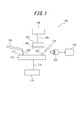
- FIG. 1 is a schematic view of a wafer single-side polishing apparatus 100 according to an embodiment of the present invention.
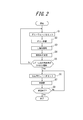
- 3 is a flowchart illustrating a wafer polishing method according to an embodiment of the present invention. It is a graph which shows LPD of the wafer after grinding
- polishing in a comparative example and an invention example. 1 is a schematic view of a conventional wafer single-side polishing apparatus 200.
- the wafer single-side polishing apparatus 100 includes a head 102 for fixing the wafer 104 and a surface plate 110 provided with a polishing cloth 112 on the surface.
- the head 102 is connected to a motor 108 via a head elevating shaft 106, and the motor 108 is driven to rotate the head 102 and the wafer 104.
- the surface plate 110 is connected to a motor 116 via a surface plate rotation shaft 114 and drives the motor 116 to rotate the surface plate 110.
- the wafer 104 fixed to the head 102 is brought into contact with the polishing cloth 112 and the head 102 and the surface plate 110 are rotated together while supplying the polishing liquid 128 from the polishing liquid supply unit 126 onto the polishing cloth 112, thereby Polish the surface to be polished.
- the wafer single-side polishing apparatus 100 includes a contact angle meter 122 that measures the contact angle of the polishing pad 112.
- the contact angle meter 122 measures the contact angle of the water droplet 120 dripped on the polishing pad 112 from the water droplet supply unit 118. Thereby, the surface state of the polishing pad 112 can be grasped.
- the control part 124 is arbitrary structures in this invention, it receives the input of the data of a measured value from the contact angle meter 122. FIG. The function of the control unit 124 will be described later.
- the type of polishing cloth 112 is not limited.
- a single-layer type polishing cloth or a two-layer type polishing cloth in which a sponge layer is formed on the back surface of the polishing cloth layer may be used.
- a polishing cloth made of a synthetic resin foam such as urethane foam for example, a hard velor type polishing in which a polyester fiber nonwoven fabric is impregnated with a urethane resin
- a suede pad in which a urethane resin is foamed on a cloth or a non-woven fabric base cloth can be employed.
- the location on the polishing pad 112 for supplying the water droplet 120 is not limited as long as the wafer 104 passes through at the time of polishing.
- polishing liquid 1208 for example, an alkaline polishing liquid containing colloidal silica or the like as abrasive grains is used.
- the place for supplying the polishing liquid is not particularly limited, but it is preferable to supply the polishing liquid in the vicinity of the rotation track in the center of the head 102.
- the present inventor sequentially finished and polished a plurality of wafers one by one with two new polishing cloths (polishing cloths A and B), both of which are suede materials. .
- polishing cloths A and B both of which are suede materials.
- the contact angle of the polishing cloth was measured.
- the number of LPDs of the polished wafer was measured with a laser particle counter.
- the first 20 polishings were regarded as dummy polishing, and the contact angle of the polishing cloth and the LPD measurement of the polished wafer were not performed.
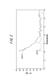
- FIG. 3 shows the relationship between the cumulative number of polished sheets and the number of LPDs for each of the polishing pad A and the polishing pad B.
- polishing cloth A the number of LPDs of the 21st wafer is very large, more than 350, and as the polishing cloth A is further polished, the number of LPDs decreases, and the 40th and subsequent wafers have about 50 LPDs. And stable.
- the polishing pad B the LPD was already below 50 pieces in the 21st wafer, and the LPD was stabilized at around 50 pieces even in the polished wafer after that.
- FIG. 4 shows the relationship between the accumulated number of polishing and the contact angle of the polishing cloth for each of the polishing cloth A and the polishing cloth B.
- the contact angle measured immediately before polishing the 21st wafer is relatively high, about 65 degrees, and is in a water-repellent state. Then, as the polishing pad A is repeatedly polished, the contact angle of the polishing pad also decreases. The contact angle immediately before polishing about the 40th and subsequent wafers was stable in a hydrophilic state in the range of 20 to 30 degrees.
- the polishing pad B the contact angle of the 21st wafer immediately before polishing was already about 25 degrees, and after that, the contact angle of the polishing cloth was stable in the range of 20 to 30 degrees.
- the wafer polished with a high contact angle of the polishing cloth has a large amount of LPD, and the wafer polished with a low state has a low LPD. It was found that there was a good correlation with the number of LPDs on the wafer.
- the number of dummy polishing is not set to 20 uniformly, but every time or periodically before polishing.
- the contact angle is measured and it is confirmed that the contact angle falls to a range of 20 to 30 degrees and is stabilized, the subsequent polishing is determined as the main polishing.
- a polishing cloth of the same type as the polishing cloths A and B is installed on the surface of the surface plate, and the polishing method of this embodiment is started.
- a dummy wafer is fixed to the head (step S1), and the set wafer is polished as a dummy polishing step (step S2).
- the polished dummy wafer is removed from the head, and the surface plate is rotated to remove the polishing liquid on the polishing cloth (step S3). Thereafter, the contact angle of the polishing pad is measured (step S4).
- step S5 Based on the measured value of the contact angle, it is determined whether or not the measured value within ⁇ 3 degrees is continued three times or more (step S5). If this condition is not satisfied, the process returns to step S1 again to perform a dummy polishing process. That is, after the first and second dummy polishings, the determination is automatically “No”.
- step S5 when it is determined in step S5 that the measured value within ⁇ 3 degrees is continuous three times or more, the process proceeds to the polishing process. That is, the product wafer is fixed to the head (step S6), and as a main polishing process, the set product wafer is subjected to final polishing (step S7). All subsequent polishing can be the main polishing step. That is, when the polishing is not completed (step S8), the product wafer after the previous polishing is removed from the head, a new product wafer is fixed to the head (step S6), and the main polishing process (step S7) is performed again. And repeat this. When the polishing is finished (step S8), the present method is finished.
- the polishing after the 40th time is the main polishing, and the polishing cloth having the same properties as the polishing cloth B is used.
- polishing after less than the 20th time (for example, the 15th time) will be the main polishing.
- the contact angle of the polishing cloth is measured as described above, and the initial polishing process (dummy polishing process) is started based on the measured value.
- the timing for switching to the main polishing process is determined. Therefore, wafer loss due to dummy polishing can be reduced, and the number of LPDs of product wafers can be stabilized at a small level.
- the polishing cloth is nondestructive and has high practicality.
- the contact angle of the polishing cloth is measured every time or periodically after the polishing process as described above, and when the measured value is stabilized, the next polishing process can be determined as the main polishing process.
- the measured value within ⁇ 3 degrees continues three times or more (that is, when the three measured values are within ⁇ 3 degrees for the first time)
- the measured value is stable (asymptotic state). I decided to consider it.
- the convergence value of the contact angle varies somewhat depending on the type of polishing cloth, but this definition can be applied regardless of the type of polishing cloth.
- step S2 in FIG. 2 is set to “whether the measured value of the contact angle is equal to or less than a predetermined value. You may make it judge by. For example, if the measured value exceeds 30 degrees in step S5, the process returns to the dummy polishing process (step S2), and if it is 30 degrees or less, the process proceeds to the main polishing process (step S6). As described above, when the measured value of the contact angle of the polishing pad is equal to or less than the threshold value, the subsequent polishing process can be determined as the main polishing process.
- this threshold is measured by repeatedly performing the polishing treatment and the measurement of the contact angle of the test polishing cloth using the same type of test polishing cloth as the polishing cloth used in the final polishing (in the above case, the polishing cloths A and B). It is determined based on the value when the measured value of the contact angle of the polishing cloth is stabilized. In this embodiment, since the contact angles of the polishing cloths A and B are stable within a range of 20 to 30 degrees, 30 degrees is set as a threshold value. As described above, whether or not the measured value is stable is determined based on whether or not the measured value within ⁇ 3 degrees is continued three times or more.
- the method for determining the threshold value is not particularly limited, and may be, for example, the above average value of three times or the maximum value of three times. In this embodiment, the contact angle is measured based on the ⁇ / 2 method by dropping 1000 ⁇ g of water.
- the measurement of the contact angle of the polishing cloth is not limited to being performed every time after the dummy polishing step as shown in FIG.
- the contact angle may be measured once every two dummy polishing steps. If the minimum number of dummy polishings required is empirically known, the contact angle measurement may be started after the number of dummy polishings.
- the wafer used for the dummy polishing step does not become a product, it is preferable to use a dummy wafer having a lower cost than the product wafer.
- the contact angle of the polishing cloth can be measured even after the main polishing step, and the replacement timing of the polishing cloth in the main polishing step can be determined based on the measured value. That is, the contact angle of the polishing cloth is also an effective index for judging the life of the polishing cloth.
- Abrasive cloth is a consumable item, and until now it has been discarded after being used for polishing a predetermined number of times and replaced with a new abrasive cloth. However, the number of polishing until the polishing cloth is actually unusable varies depending on the polishing cloth or depending on the polishing conditions, and determine whether the polishing cloth can be used.
- the predetermined number of times has been set with a margin within a range where the polishing cloth can still be used.
- the contact angle of the polishing cloth gradually increased from the final polishing step toward the end of use. Therefore, the stage where the contact angle takes a predetermined threshold can be set as the use limit of the polishing pad.
- the contact angle is measured after the final polishing step, and if the measured value is less than or equal to a predetermined threshold value, the polishing cloth can still be used and is used as it is in the subsequent main polishing step. If it exceeds, the abrasive cloth is no longer usable and prompts replacement. In this way, by grasping the surface state of the polishing cloth from the contact angle of the polishing cloth and accurately determining the replacement time of the polishing cloth, the polishing cloth can be used to the end of the original service life of the polishing cloth. . For this reason, the wafer manufacturing cost can be reduced.
- the threshold value of the contact angle of the polishing cloth depends on the type, hardness, coefficient of restitution, etc. of the polishing cloth, but can be set to 70 degrees, for example. Further, the life determination based on the contact angle of the polishing cloth described here may be performed independently of the determination of the switching timing from the dummy polishing step to the main polishing step based on the contact angle of the polishing cloth described above.
- the single-sided finish polishing method for polishing one wafer at a time has been described, but the present invention is not limited to this, and is applied to a method for polishing a plurality of wafers at a time and a double-side polishing method. You can also
- the determination of the switching time from the dummy polishing step to the main polishing step and the replacement timing of the polishing cloth based on the contact angle measurement value may be automatically performed by the control unit 124 shown in FIG. .
- the single-side polishing apparatus 100 has a memory (not shown). In this memory, data of a threshold A (30 degrees in this embodiment) when switching from a dummy polishing process to a main polishing process, and polishing are performed. Data of a threshold value B (70 degrees in the present embodiment) for cloth replacement is stored.
- control unit 124 When the control unit 124 receives the output of the measurement value of the contact angle of the polishing pad 112 output from the contact angle meter 122 in the dummy polishing step, the control unit 124 reads the data of the threshold value A from the memory, In comparison, it is determined whether the subsequent polishing should be the dummy polishing step or the main polishing step.
- the control unit 124 records the determination result (more specifically, the combination of the cumulative polishing number n and the determination result) in the memory.
- control unit 124 when the control unit 124 receives the output of the measured value of the contact angle of the polishing pad 112 output from the contact angle meter 122 in the stage of the dummy polishing process, the measured value within the range of ⁇ 3 degrees is measured three times or more. It is determined whether or not it is continuous, and it is determined whether or not the next polishing should be the dummy polishing step or the main polishing step.
- the control unit 124 records the determination result (more specifically, the combination of the cumulative polishing number n and the determination result) in the memory.
- the user of the single-side polishing apparatus 100 can grasp from which wafer the product wafer should be a product wafer if the determination result is read from the memory afterwards.
- the control unit 124 may individually notify the determination result to a notification unit such as a speaker or a display.
- the control unit 124 When the control unit 124 receives the output of the measurement value of the contact angle of the polishing pad 112 output from the contact angle meter 122 in the stage of the main polishing process, the control unit 124 reads the data of the threshold value B from the memory, In comparison, it is determined whether or not the polishing cloth should be replaced. For example, the control unit 124 may record the determination result in a memory. Further, when the measured value exceeds the threshold value B, the control unit 124 does not drive the motors 108 and 116. The control unit 124 may prompt the replacement of the polishing cloth by a notification means such as a speaker or a display.
- a notification means such as a speaker or a display.
- polishing was performed according to the flow of FIG. That is, after the measurement value within ⁇ 3 degrees was continued three times or more, this polishing step was set. As a result, after performing the dummy polishing step 42 times, this polishing step was started. In this experiment, the polishing process was performed 100 times.
- the contact angle of the polishing pad when this polishing process was completed was 28 degrees. Thereafter, the polishing of the silicon wafer and the measurement of the contact angle were further continued alternately, and the change in the contact angle was investigated. As a result, a tendency for the contact angle to increase greatly after 252 main polishing steps was observed. Conventionally, in order to surely avoid mixing of wafers with a large amount of LPD, this polishing cloth has been replaced by polishing about 200 times. Therefore, it is possible to use the polishing cloth to the limit of the original service life.
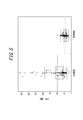
- the surface of the wafer polished in this polishing step was measured with a laser particle counter (manufactured by KLA-Tencorr, SP-3) to determine the number of LPDs. The results are shown in FIG.
- the dummy polishing process was set to 20 times, and the polishing process was performed 100 times as the main polishing process after the 21st time.
- the number of LPDs of the wafer polished in this polishing step was determined in the same manner as in the inventive examples. The results are shown in FIG.
- the wafer loss due to dummy polishing can be reduced and the number of LPDs of product wafers can be stabilized at a low level by a practical method. .
Landscapes
- Engineering & Computer Science (AREA)
- Mechanical Engineering (AREA)
- Finish Polishing, Edge Sharpening, And Grinding By Specific Grinding Devices (AREA)
- Mechanical Treatment Of Semiconductor (AREA)
Abstract
Description
本発明のウェーハの研磨方法は、
定盤の表面に設けられた研磨布にウェーハを接触させて、前記定盤および前記ウェーハを回転させることで、前記ウェーハ表面を研磨する研磨処理を、同一研磨布により複数回行うウェーハの研磨方法であって、
前記研磨処理は、研磨後のウェーハを製品としない初期研磨工程と、前記初期研磨工程後、研磨後のウェーハを製品とする本研磨工程とからなり、
前記研磨布の接触角を測定し、その測定値に基づいて、前記初期研磨工程から前記本研磨工程への切替え時期を決定することを特徴とする。
ウェーハを保持する保持部と、表面に研磨布を有する定盤とを有し、前記研磨布に前記ウェーハを接触させて、前記定盤および前記ウェーハを回転させることで、前記ウェーハ表面を研磨する研磨処理を、同一研磨布により複数回行うウェーハの研磨装置であって、
前記研磨布の接触角を測定する測定装置と、
該測定装置により得られた測定値に基づいて、研磨後のウェーハを製品としない初期研磨工程から、研磨後のウェーハを製品とする本研磨工程への切替え時期を決定する制御部と、
をさらに有することを特徴とする。
次に、図2~4を参照して、本発明の一実施形態によるウェーハの片面研磨方法を説明する。
直径300mmのシリコンウェーハを用いて実験を行った。図3,4の実験を行った研磨布と同種のスウェード素材の研磨布を、図1に示す片面研磨装置の定盤上に設置した。この片面研磨装置により、1枚ずつシリコンウェーハの仕上げ研磨を行った。研磨条件は以下のとおりとした。
研磨圧力:125g/cm2
研磨時間:360秒
研磨液:アルカリ研磨液(コロイダルシリカ含有)
直径300mmのシリコンウェーハを用いて実験を行った。図3,4の実験を行った研磨布と同種のスウェード素材の研磨布を、図6に示す片面研磨装置の定盤上に設置した。この片面研磨装置により、1枚ずつシリコンウェーハの仕上げ研磨を行った。研磨条件は発明例と同じとした。
図5から明らかなとおり、比較例では、本研磨工程をうけたウェーハの中にLPDの数が多いウェーハが混在してしまい、LPD数のばらつきが大きかった。比較例で用いた研磨布は、図3,4における研磨布Aと同様の性質を持った研磨布であったことがわかる。一方、発明例では、ダミー研磨回数が42回であったことから、やはり研磨布Aと同様の性質を持った研磨布を用いたことがわかるが、本研磨工程を受けたウェーハのLPDの数を少ないレベルで安定させることができた。なお、比較例ではLPD数の平均は97.4個、標準偏差は79.4であったのに対し、発明例ではLPD数の平均は45.8個、標準偏差は13.9であった。
102 ヘッド
104 ウェーハ
106 ヘッド昇降軸
108 モータ
110 定盤
112 研磨布
114 定盤回転軸
116 モータ
118 水滴供給部
120 水滴
122 接触角計
124 制御部
126 研磨液供給部
128 研磨液
Claims (8)
- 定盤の表面に設けられた研磨布にウェーハを接触させて、前記定盤および前記ウェーハを回転させることで、前記ウェーハ表面を研磨する研磨処理を、同一研磨布により複数回行うウェーハの研磨方法であって、
前記研磨処理は、研磨後のウェーハを製品としない初期研磨工程と、前記初期研磨工程後、研磨後のウェーハを製品とする本研磨工程とからなり、
前記研磨布の接触角を測定し、その測定値に基づいて、前記初期研磨工程から前記本研磨工程への切替え時期を決定することを特徴とするウェーハの研磨方法。 - 前記研磨処理の前に毎回または定期的に前記研磨布の接触角を測定し、測定値が安定した後の研磨処理を前記本研磨工程と決定する請求項1に記載のウェーハの研磨方法。
- 前記測定値が閾値以下である場合に、以後の研磨処理を前記本研磨工程と決定する請求項1に記載のウェーハの研磨方法。
- 前記研磨布と同種の試験研磨布を用いて、前記研磨処理と前記試験研磨布の接触角の測定とをくり返し行い、該試験研磨布の接触角の測定値が安定したときの値に基づき前記閾値を決定する請求項3に記載のウェーハの研磨方法。
- 前記研磨布の接触角を測定する直前に、前記定盤を回転させて前記研磨布上の研磨液を除去する請求項1~4のいずれか1項に記載のウェーハの研磨方法。
- 前記初期研磨工程で研磨される前記ウェーハがダミーウェーハである請求項1~5のいずれか1項に記載のウェーハの研磨方法。
- 前記初期研磨工程から前記本研磨工程に切り替えた後に、前記研磨布の接触角を再度測定し、その測定値に基づいて前記本研磨工程における前記研磨布の交換時期を決定する請求項1~6のいずれか1項に記載のウェーハの研磨方法。
- ウェーハを保持する保持部と、表面に研磨布を有する定盤とを有し、前記研磨布に前記ウェーハを接触させて、前記定盤および前記ウェーハを回転させることで、前記ウェーハ表面を研磨する研磨処理を、同一研磨布により複数回行うウェーハの研磨装置であって、
前記研磨布の接触角を測定する測定装置と、
該測定装置により得られた測定値に基づいて、研磨後のウェーハを製品としない初期研磨工程から、研磨後のウェーハを製品とする本研磨工程への切替え時期を決定する制御部と、
をさらに有することを特徴とするウェーハの研磨装置。
Priority Applications (5)
| Application Number | Priority Date | Filing Date | Title |
|---|---|---|---|
| JP2015533944A JP6008053B2 (ja) | 2013-08-28 | 2014-06-24 | ウェーハの研磨方法およびウェーハの研磨装置 |
| US14/914,747 US9919402B2 (en) | 2013-08-28 | 2014-06-24 | Method of polishing wafer and wafer polishing apparatus |
| KR1020167005150A KR101736738B1 (ko) | 2013-08-28 | 2014-06-24 | 웨이퍼의 연마 방법 및 웨이퍼의 연마 장치 |
| DE112014003946.2T DE112014003946B4 (de) | 2013-08-28 | 2014-06-24 | Verfahren zum Waferpolieren |
| CN201480047490.9A CN105659361B (zh) | 2013-08-28 | 2014-06-24 | 晶片的研磨方法及晶片的研磨装置 |
Applications Claiming Priority (2)
| Application Number | Priority Date | Filing Date | Title |
|---|---|---|---|
| JP2013-176931 | 2013-08-28 | ||
| JP2013176931 | 2013-08-28 |
Publications (1)
| Publication Number | Publication Date |
|---|---|
| WO2015029294A1 true WO2015029294A1 (ja) | 2015-03-05 |
Family
ID=52585894
Family Applications (1)
| Application Number | Title | Priority Date | Filing Date |
|---|---|---|---|
| PCT/JP2014/003393 Ceased WO2015029294A1 (ja) | 2013-08-28 | 2014-06-24 | ウェーハの研磨方法およびウェーハの研磨装置 |
Country Status (7)
| Country | Link |
|---|---|
| US (1) | US9919402B2 (ja) |
| JP (1) | JP6008053B2 (ja) |
| KR (1) | KR101736738B1 (ja) |
| CN (1) | CN105659361B (ja) |
| DE (1) | DE112014003946B4 (ja) |
| TW (1) | TWI528441B (ja) |
| WO (1) | WO2015029294A1 (ja) |
Cited By (2)
| Publication number | Priority date | Publication date | Assignee | Title |
|---|---|---|---|---|
| JP2023167965A (ja) * | 2022-05-13 | 2023-11-24 | 株式会社荏原製作所 | 処理システム、パッド搬送装置、液受け装置、および研磨装置 |
| US20230415300A1 (en) * | 2020-09-30 | 2023-12-28 | Fujibo Holdings, Inc. | Polishing pad and method for manufacturing polishing pad |
Families Citing this family (3)
| Publication number | Priority date | Publication date | Assignee | Title |
|---|---|---|---|---|
| KR101962090B1 (ko) | 2018-12-03 | 2019-03-26 | 권종진 | 웨이퍼 폴리싱 장치 및 그 방법 |
| JP6809626B1 (ja) * | 2020-04-08 | 2021-01-06 | 信越半導体株式会社 | シリコンウェーハのdic欠陥の形状測定方法及び研磨方法 |
| JP6780800B1 (ja) * | 2020-04-09 | 2020-11-04 | 信越半導体株式会社 | ウェーハの研磨方法及び研磨装置 |
Citations (4)
| Publication number | Priority date | Publication date | Assignee | Title |
|---|---|---|---|---|
| US5851138A (en) * | 1996-08-15 | 1998-12-22 | Texas Instruments Incorporated | Polishing pad conditioning system and method |
| US5990012A (en) * | 1998-01-27 | 1999-11-23 | Micron Technology, Inc. | Chemical-mechanical polishing of hydrophobic materials by use of incorporated-particle polishing pads |
| JP2005209863A (ja) * | 2004-01-22 | 2005-08-04 | Komatsu Electronic Metals Co Ltd | 研磨用クロス及び半導体ウェーハの研磨方法 |
| JP2005342881A (ja) * | 2004-05-07 | 2005-12-15 | Nitta Haas Inc | 研磨パッド、研磨方法および研磨装置 |
Family Cites Families (10)
| Publication number | Priority date | Publication date | Assignee | Title |
|---|---|---|---|---|
| US5433650A (en) * | 1993-05-03 | 1995-07-18 | Motorola, Inc. | Method for polishing a substrate |
| US6361409B1 (en) * | 1999-09-28 | 2002-03-26 | Rodel Holdings Inc. | Polymeric polishing pad having improved surface layer and method of making same |
| JP2002059357A (ja) * | 2000-08-23 | 2002-02-26 | Toray Ind Inc | 研磨パッドおよび研磨装置ならびに研磨方法 |
| KR100877385B1 (ko) * | 2001-11-13 | 2009-01-07 | 도요 고무 고교 가부시키가이샤 | 연마 패드 및 그 제조 방법 |
| JP2004335713A (ja) * | 2003-05-07 | 2004-11-25 | Rodel Nitta Co | 仕上げ研磨用研磨布 |
| JP2006147980A (ja) * | 2004-11-24 | 2006-06-08 | Fujitsu Ltd | 研磨方法 |
| US20090061743A1 (en) | 2007-08-29 | 2009-03-05 | Stephen Jew | Method of soft pad preparation to reduce removal rate ramp-up effect and to stabilize defect rate |
| US9951054B2 (en) * | 2009-04-23 | 2018-04-24 | Cabot Microelectronics Corporation | CMP porous pad with particles in a polymeric matrix |
| JP5900196B2 (ja) * | 2012-07-05 | 2016-04-06 | 株式会社Sumco | ウェーハの片面研磨方法およびウェーハの片面研磨装置 |
| US10391605B2 (en) * | 2016-01-19 | 2019-08-27 | Applied Materials, Inc. | Method and apparatus for forming porous advanced polishing pads using an additive manufacturing process |
-
2014
- 2014-06-24 KR KR1020167005150A patent/KR101736738B1/ko active Active
- 2014-06-24 US US14/914,747 patent/US9919402B2/en active Active
- 2014-06-24 JP JP2015533944A patent/JP6008053B2/ja active Active
- 2014-06-24 WO PCT/JP2014/003393 patent/WO2015029294A1/ja not_active Ceased
- 2014-06-24 CN CN201480047490.9A patent/CN105659361B/zh active Active
- 2014-06-24 DE DE112014003946.2T patent/DE112014003946B4/de active Active
- 2014-08-11 TW TW103127409A patent/TWI528441B/zh active
Patent Citations (4)
| Publication number | Priority date | Publication date | Assignee | Title |
|---|---|---|---|---|
| US5851138A (en) * | 1996-08-15 | 1998-12-22 | Texas Instruments Incorporated | Polishing pad conditioning system and method |
| US5990012A (en) * | 1998-01-27 | 1999-11-23 | Micron Technology, Inc. | Chemical-mechanical polishing of hydrophobic materials by use of incorporated-particle polishing pads |
| JP2005209863A (ja) * | 2004-01-22 | 2005-08-04 | Komatsu Electronic Metals Co Ltd | 研磨用クロス及び半導体ウェーハの研磨方法 |
| JP2005342881A (ja) * | 2004-05-07 | 2005-12-15 | Nitta Haas Inc | 研磨パッド、研磨方法および研磨装置 |
Cited By (3)
| Publication number | Priority date | Publication date | Assignee | Title |
|---|---|---|---|---|
| US20230415300A1 (en) * | 2020-09-30 | 2023-12-28 | Fujibo Holdings, Inc. | Polishing pad and method for manufacturing polishing pad |
| JP2023167965A (ja) * | 2022-05-13 | 2023-11-24 | 株式会社荏原製作所 | 処理システム、パッド搬送装置、液受け装置、および研磨装置 |
| JP7746217B2 (ja) | 2022-05-13 | 2025-09-30 | 株式会社荏原製作所 | 処理システムおよびパッド搬送装置 |
Also Published As
| Publication number | Publication date |
|---|---|
| US20160207161A1 (en) | 2016-07-21 |
| TWI528441B (zh) | 2016-04-01 |
| JPWO2015029294A1 (ja) | 2017-03-02 |
| DE112014003946T5 (de) | 2016-05-19 |
| CN105659361B (zh) | 2018-06-12 |
| KR20160039255A (ko) | 2016-04-08 |
| TW201513199A (zh) | 2015-04-01 |
| KR101736738B1 (ko) | 2017-05-17 |
| US9919402B2 (en) | 2018-03-20 |
| JP6008053B2 (ja) | 2016-10-19 |
| DE112014003946B4 (de) | 2020-11-26 |
| CN105659361A (zh) | 2016-06-08 |
Similar Documents
| Publication | Publication Date | Title |
|---|---|---|
| TWI353006B (en) | Method for manufacturing epitaxial wafer | |
| JP6008053B2 (ja) | ウェーハの研磨方法およびウェーハの研磨装置 | |
| JP6312976B2 (ja) | 半導体ウェーハの製造方法 | |
| US11170988B2 (en) | Method of double-side polishing silicon wafer | |
| JP6327329B1 (ja) | シリコンウェーハの研磨方法およびシリコンウェーハの製造方法 | |
| TWI553722B (zh) | Silicon wafer manufacturing method and silicon wafer | |
| JP6027346B2 (ja) | 半導体ウェーハの製造方法 | |
| JP2002231669A (ja) | 半導体ウェーハ用研磨布およびこれを用いた半導体ウェーハの研磨方法 | |
| TW553806B (en) | Method and device for polishing semiconductor wafer | |
| JP2006095677A (ja) | 研磨方法 | |
| JP5900196B2 (ja) | ウェーハの片面研磨方法およびウェーハの片面研磨装置 | |
| KR101767059B1 (ko) | 화학 기계적 기판 연마장치 | |
| JP2008068338A (ja) | 研磨装置、研磨方法、および半導体装置の製造方法 | |
| JP2018049980A (ja) | 半導体装置の製造方法 | |
| JP2021106226A (ja) | 半導体ウェーハ用研磨布の使用開始時期の判定方法及びそれを用いた半導体ウェーハの研磨方法、並びに半導体ウェーハ研磨システム | |
| TWI851227B (zh) | 晶圓的單面拋光方法、晶圓的製造方法、及晶圓的單面拋光裝置 | |
| JP6248857B2 (ja) | 研磨布の評価方法 | |
| JP2010218643A (ja) | ガラス基板の製造方法、ガラス基板及び磁気記録媒体 | |
| KR101581469B1 (ko) | 웨이퍼 연마방법 | |
| WO2006035865A1 (ja) | 半導体ウェーハの製造方法及び半導体ウェーハ | |
| JP2003100668A (ja) | 半導体ウェーハの研磨方法 | |
| JP2004319717A (ja) | 半導体ウェーハの製造方法 | |
| JP2005072150A (ja) | 片面鏡面ウェーハおよびその製造方法 | |
| JP2003109990A (ja) | 半導体ウェーハの平坦度評価方法 | |
| JP2005123483A (ja) | 半導体ウェーハのプラズマエッチング方法 |
Legal Events
| Date | Code | Title | Description |
|---|---|---|---|
| 121 | Ep: the epo has been informed by wipo that ep was designated in this application |
Ref document number: 14840419 Country of ref document: EP Kind code of ref document: A1 |
|
| ENP | Entry into the national phase |
Ref document number: 2015533944 Country of ref document: JP Kind code of ref document: A |
|
| ENP | Entry into the national phase |
Ref document number: 20167005150 Country of ref document: KR Kind code of ref document: A |
|
| WWE | Wipo information: entry into national phase |
Ref document number: 14914747 Country of ref document: US |
|
| WWE | Wipo information: entry into national phase |
Ref document number: 112014003946 Country of ref document: DE Ref document number: 1120140039462 Country of ref document: DE |
|
| 122 | Ep: pct application non-entry in european phase |
Ref document number: 14840419 Country of ref document: EP Kind code of ref document: A1 |