WO2015025860A1 - 電圧型マルチレベル変換器 - Google Patents
電圧型マルチレベル変換器 Download PDFInfo
- Publication number
- WO2015025860A1 WO2015025860A1 PCT/JP2014/071699 JP2014071699W WO2015025860A1 WO 2015025860 A1 WO2015025860 A1 WO 2015025860A1 JP 2014071699 W JP2014071699 W JP 2014071699W WO 2015025860 A1 WO2015025860 A1 WO 2015025860A1
- Authority
- WO
- WIPO (PCT)
- Prior art keywords
- voltage
- short circuit
- capacitor
- change rate
- phase
- Prior art date
- Legal status (The legal status is an assumption and is not a legal conclusion. Google has not performed a legal analysis and makes no representation as to the accuracy of the status listed.)
- Ceased
Links
Images


Classifications
-
- H—ELECTRICITY
- H02—GENERATION; CONVERSION OR DISTRIBUTION OF ELECTRIC POWER
- H02M—APPARATUS FOR CONVERSION BETWEEN AC AND AC, BETWEEN AC AND DC, OR BETWEEN DC AND DC, AND FOR USE WITH MAINS OR SIMILAR POWER SUPPLY SYSTEMS; CONVERSION OF DC OR AC INPUT POWER INTO SURGE OUTPUT POWER; CONTROL OR REGULATION THEREOF
- H02M7/00—Conversion of AC power input into DC power output; Conversion of DC power input into AC power output
- H02M7/42—Conversion of DC power input into AC power output without possibility of reversal
- H02M7/44—Conversion of DC power input into AC power output without possibility of reversal by static converters
- H02M7/48—Conversion of DC power input into AC power output without possibility of reversal by static converters using discharge tubes with control electrode or semiconductor devices with control electrode
- H02M7/483—Converters with outputs that each can have more than two voltages levels
- H02M7/487—Neutral point clamped inverters
-
- H—ELECTRICITY
- H02—GENERATION; CONVERSION OR DISTRIBUTION OF ELECTRIC POWER
- H02M—APPARATUS FOR CONVERSION BETWEEN AC AND AC, BETWEEN AC AND DC, OR BETWEEN DC AND DC, AND FOR USE WITH MAINS OR SIMILAR POWER SUPPLY SYSTEMS; CONVERSION OF DC OR AC INPUT POWER INTO SURGE OUTPUT POWER; CONTROL OR REGULATION THEREOF
- H02M7/00—Conversion of AC power input into DC power output; Conversion of DC power input into AC power output
- H02M7/42—Conversion of DC power input into AC power output without possibility of reversal
- H02M7/44—Conversion of DC power input into AC power output without possibility of reversal by static converters
- H02M7/48—Conversion of DC power input into AC power output without possibility of reversal by static converters using discharge tubes with control electrode or semiconductor devices with control electrode
- H02M7/483—Converters with outputs that each can have more than two voltages levels
- H02M7/4837—Flying capacitor converters
-
- H—ELECTRICITY
- H02—GENERATION; CONVERSION OR DISTRIBUTION OF ELECTRIC POWER
- H02M—APPARATUS FOR CONVERSION BETWEEN AC AND AC, BETWEEN AC AND DC, OR BETWEEN DC AND DC, AND FOR USE WITH MAINS OR SIMILAR POWER SUPPLY SYSTEMS; CONVERSION OF DC OR AC INPUT POWER INTO SURGE OUTPUT POWER; CONTROL OR REGULATION THEREOF
- H02M1/00—Details of apparatus for conversion
- H02M1/0095—Hybrid converter topologies, e.g. NPC mixed with flying capacitor, thyristor converter mixed with MMC or charge pump mixed with buck
-
- H—ELECTRICITY
- H02—GENERATION; CONVERSION OR DISTRIBUTION OF ELECTRIC POWER
- H02M—APPARATUS FOR CONVERSION BETWEEN AC AND AC, BETWEEN AC AND DC, OR BETWEEN DC AND DC, AND FOR USE WITH MAINS OR SIMILAR POWER SUPPLY SYSTEMS; CONVERSION OF DC OR AC INPUT POWER INTO SURGE OUTPUT POWER; CONTROL OR REGULATION THEREOF
- H02M1/00—Details of apparatus for conversion
- H02M1/32—Means for protecting converters other than automatic disconnection
- H02M1/34—Snubber circuits
- H02M1/346—Passive non-dissipative snubbers
-
- Y—GENERAL TAGGING OF NEW TECHNOLOGICAL DEVELOPMENTS; GENERAL TAGGING OF CROSS-SECTIONAL TECHNOLOGIES SPANNING OVER SEVERAL SECTIONS OF THE IPC; TECHNICAL SUBJECTS COVERED BY FORMER USPC CROSS-REFERENCE ART COLLECTIONS [XRACs] AND DIGESTS
- Y02—TECHNOLOGIES OR APPLICATIONS FOR MITIGATION OR ADAPTATION AGAINST CLIMATE CHANGE
- Y02B—CLIMATE CHANGE MITIGATION TECHNOLOGIES RELATED TO BUILDINGS, e.g. HOUSING, HOUSE APPLIANCES OR RELATED END-USER APPLICATIONS
- Y02B70/00—Technologies for an efficient end-user side electric power management and consumption
- Y02B70/10—Technologies improving the efficiency by using switched-mode power supplies [SMPS], i.e. efficient power electronics conversion e.g. power factor correction or reduction of losses in power supplies or efficient standby modes
Definitions
- the present invention relates to a voltage type multi-level converter using a flying capacitor.
- switching elements In recent years, multilevel converters have become mainstream in variable speed drive devices and power conversion devices using power devices (for example, IGBTs, etc .: hereinafter referred to as switching elements).
- FIG. 6 is a diagram showing an example of a conventional voltage type multi-level converter.
- the voltage type multilevel converter shown in FIG. 6 has first and second capacitors C1 and C2 connected in series between positive and negative electrodes of a DC voltage source (not shown) and current change rate suppressing reactors L1 and L2
- a phase module 4 having snubber circuits 1a and 1b for suppressing surge voltage, current change rate detection units 3a and 3b for detecting current change rates di / dt in current change rate suppressing reactors L1 and L2, and flying capacitors C3 and C4. And have.
- FIG. 6 only one phase module 4 is shown for simplification.
- phase module 4 In the voltage type multi-level converter shown in FIG. 6, it is determined that a short circuit has occurred in phase module 4 when current change rate detected value di / dt output from current change rate detectors 3a and 3b is equal to or more than a predetermined value.
- a short circuit abnormality signal is transmitted to a controller (not shown) in the phase module 4 via a common controller (not shown). Thereafter, the controller in the phase module 4 transmits a gate shutoff signal to the drive circuit of the switching element to shut off the gate signal safely.
- the load of the device has a predetermined current waveform, and the current change rate di / dt of the flying capacitor accompanying this is known, and therefore, is set in advance as a reference value, and this reference value and the current change rate detection units 3a and 3b.
- the short circuit judgment can be made by comparing with the current change rate detected value di / dt of
- the first and second capacitors C1 and C2 connected to the DC voltage source and the current change rate suppressing reactors L1 and L2 are common to each phase module 4 It is provided only in one place. Therefore, when a short circuit abnormality occurs, the current change rate detection value di / dt needs to transmit a short circuit abnormality signal to the controller in the phase module 4 via the common controller. As a result, it is necessary to speed up the communication speed between the common controller and the controller in the phase module 4 or to suppress the short circuit current by providing larger current change rate suppressing reactors L1 and L2 and snubber circuits 1a and 1b. was there.
- the present invention was devised in view of the above-mentioned conventional problems, and one aspect thereof is a voltage type multi-level converter which generates an AC output obtained by converting a DC voltage into a plurality of voltage levels, which is a DC voltage
- a capacitor common to each phase connected in series between both terminals of the source, a flying capacitor provided for each phase and charged with a voltage different from that of the capacitor, and a plurality of switching elements for each phase
- a voltage selection circuit selectively outputting a plurality of voltage levels based on voltages of the capacitor and the flying capacitor by selectively turning on and off the switching element, and detecting a rate of change in voltage across the flying capacitor Detecting a short circuit when the voltage change rate across the flying capacitor exceeds a threshold value.
- a short circuit abnormality signal is outputted to a controller in a phase module when a voltage change rate across the flying capacitor exceeds a threshold.
- the cause of the short circuit is identified by the value of the rate of change in voltage across the flying capacitor.
- FIG. 2 is a diagram showing an equivalent circuit of a capacitor. It is a time chart which shows each waveform at the time of normal time and a short circuit. It is a circuit block diagram which shows the voltage type
- the present invention detects, in a voltage type multi-level converter using a flying capacitor, a low impedance short circuit on an output side, an abnormality such as a sudden switching element, or a short circuit failure caused by an accidental drive circuit malfunction. It is intended to prevent the expansion of the fault range.
- FIG. 1 is a circuit configuration diagram of a voltage type multi-level converter according to the present embodiment.
- a five-level voltage type power converter is described as an example.
- first and second capacitors C1 and C2 are connected in series between positive and negative ends of a DC voltage source (not shown).
- the common connection point between the two capacitors C1 and C2 is taken as an output terminal B.
- the positive terminal of the direct current voltage source is P
- the negative terminal is N.
- the first switching element S1 and the flying capacitor C3 are sequentially connected in series.
- the Nth to sixth switching elements and the flying capacitor C4 are sequentially connected in series.
- the flying capacitors C3 and C4 are connected in series, and the first switching element S1, the flying capacitors C3 and C4, and the sixth switching element S6 constitute a first series circuit.
- the second, third, fourth and fifth switching elements S2, S3, S4 and S5 are sequentially connected in series to form a second series circuit.
- the second switching element S2 is connected to the common connection point of the first switching element S1 and the flying capacitor C3
- the fifth switching element S5 is connected to the common connection point of the sixth switching element S6 and the flying capacitor C4.
- the middle point of the second series circuit (the common connection point of the third and fourth switching elements S3 and S4) is taken as the output terminal A.
- first and second diodes D1 and D2 are interposed between the common connection point of the second and third switching elements S2 and S3 and the common connection point of the fourth and fifth switching elements S4 and S5, The common connection point of the first and second diodes D1 and D2 is connected to the common connection point of the flying capacitors C3 and C4.
- a seventh switching element S7 and an eighth switching element S8 are connected in series in the opposite direction between the output terminal B and the common connection point of the flying capacitors C3 and C4.
- the first to eighth switching elements S1 to S8 constitute a voltage selection circuit.
- Reference numerals 1a and 1b denote snubber circuits, which respectively include snubber diodes D3, D4, D5 and D6, snubber capacitors C5 and C6, feedback resistors R1 and R2, and current change suppressing reactors L1 and L2.
- the flying capacitors C3 and C4 are provided with voltage change rate detectors 2a and 2b for detecting the voltage change rate dV / dt at both ends of the flying capacitor via the voltage dividing resistors R3 and R4.
- the voltage type multi-level converter in this embodiment is the switching element in the drive circuit 7 of each switching element when the voltage of the first and second capacitors C1 and C2 is 2E and the voltage of the flying capacitors C3 and C4 is E.
- S1 to S8 By turning on and off S1 to S8 according to the switching patterns of modes 1 to 7 shown in Table 1 below, voltages 2E, E, 0, -E, and -2E of five levels can be output between output terminals AB.
- ⁇ Mode 1> The first, second, and third switching elements S1, S2, and S3 turn on, and the fourth, fifth, sixth, seventh, and eighth switching elements S4, S5, S6, S7, and S8 turn off, and the current I A Flows through the path of output terminal BBfirst capacitor C1 ⁇ P ⁇ S1 ⁇ S2 ⁇ S3 ⁇ output terminal A.
- the negative side ⁇ positive side of the first capacitor C1 is connected between the output terminals AB, and the voltage between the output terminals A and B is 2E.
- ⁇ Mode 2> The first, third and fourth switching elements S1, S3 and S4 are turned on, and the second, fifth, sixth, seventh and eighth switching elements S2, S5, S6, S7 and S8 are turned off, and the current I A Is output terminal B ⁇ first capacitor C 1 ⁇ P ⁇ S 1 ⁇ flying capacitor C 3 ⁇ D 1 ⁇ S 3 ⁇ output terminal A (or output terminal B ⁇ first capacitor C 1 ⁇ P ⁇ S 1 ⁇ flying capacitor C 3 ⁇ D 2 ⁇ S 4 ⁇ output It flows along the path of terminal A).
- ⁇ Mode 3> The second, third, seventh, eighth switching element S2, S3, S7, S8 are turned on, first, fourth, fifth, sixth switching elements S1, S4, S5, S6 are turned off, current I A Flows through a path of output terminal B ⁇ S7 ⁇ S8 ⁇ flying capacitor C3 ⁇ S2 ⁇ S3 ⁇ output terminal A.
- the negative side ⁇ positive side of the flying capacitor C3 is connected between the output terminals AB, and the voltage between the output terminals A and B is E. In this mode 3, the flying capacitor C3 is charged when the current I A > 0.
- ⁇ Mode 4> The third, fourth, seventh, eighth switching elements S3, S4, S7, S8 turn on, the first, second, fifth, sixth switching elements S1, S2, S5, S6 turn off, and the current is output terminal B ⁇ S7 ⁇ S8 ⁇ D1 ⁇ S3 ⁇ output terminal a (or, when the current I a is negative, the output terminal B ⁇ S7 ⁇ S8 ⁇ D2 ⁇ S4 ⁇ output terminal a) flows through a path of. Seventh between output terminals AB, eighth, first switching element S7, S8, S1 (or current I A is when negative seventh, eighth, second switching element S7, S8, S2) via the And the voltage between the output terminals AB becomes zero.
- ⁇ Mode 5> The fourth, fifth, seventh, eighth switching elements S4, S5, S7, S8 are turned on, the first, second, third, sixth switching elements S1, S2, S3, S6 are turned off, and the current I A Flows through the path of output terminal B ⁇ S7 ⁇ S8 ⁇ flying capacitor C4 ⁇ S5 ⁇ S4 ⁇ output terminal A.
- the positive side to the negative side of the flying capacitor C4 is connected in series between the output terminals AB, and the voltage between the output terminals A and B is -E. In this mode 5, the flying capacitor C4 is discharged when the current I A > 0.
- ⁇ Mode 7> The fourth, fifth and sixth switching elements S4, S5 and S6 are turned on, and the first, second, third, seventh and eighth switching elements S1, S2, S3, S7 and S8 are turned off, and the current I A Flows through the path of the output terminal B, the second capacitor C2, N, S6, S5, S4, and the output terminal A.
- the positive side to the negative side of the second capacitor C2 is connected between the output terminals AB, and the voltage between the output terminals A and B is -2E.
- the voltages of the flying capacitors C3 and C4 can be controlled using switching patterns (Modes 2, 3, 5, 6 in Table 1) which are charged or discharged when the output voltage V AB is E or -E. That is, although both of the output voltages in mode 2 and mode 3 are E, since the flying capacitor C3 can be charged or discharged, the voltage of the flying capacitor C3 can be adjusted. Similarly, although the output voltages of mode 5 and mode 6 are both ⁇ E, it is possible to adjust the voltage of the flying capacitor C 4 because the flying capacitor C 4 can be charged or discharged.
- the short circuit of the phase module 4 is detected by detecting the current change rate di / dt in the current change rate suppressing inductances L1 and L2 common to each phase, but this embodiment shown in FIG. In the above, the short circuit of the phase module 4 is detected by detecting the increase or decrease of the voltage change rate dV / dt in the flying capacitors C3 and C4 in the phase module 4.
- phase module 4 when a short circuit abnormality occurs in the phase module 4, the output signals of the voltage change rate detection units 2a and 2b are not driven by the controller common to each phase, and the controller 6 and the drive in each phase module 4 are driven.
- the gate signals of the switching elements S1 to S8 can be cut off only via the circuit 7.
- voltage change rate detectors 2a and 2b for detecting voltage change rates dV / dt of flying capacitors C3 and C4 are originally provided for control of the voltage type multi-level converter, so common use may be made as they are. It is possible.
- the short circuit (1) shown in FIG. 3A shows an example in which the first and second capacitors C1 and C2 and the flying capacitors C3 and C4 are connected in parallel. As described above, the voltage of the flying capacitors C3 and C4 is charged at a voltage lower than the voltage of the first and second capacitors C1 and C2. In the short circuit (1), the voltage change rate dV / dt decreases due to the discharge of the flying capacitors C3 and C4.
- the short circuit (2) shown in FIG. 3 (b) shows an example in which first and second capacitors C1 and C2 and flying capacitors C3 and C4 are connected in series as voltage sources.
- the voltage of the first and second capacitors C1 and C2 > the voltage of the flying capacitors C3 and C4. Therefore, the flying capacitors C3 and C4 are charged from the first and second capacitors C1 and C2.
- the voltage change rate dV / dt rises.
- the short circuit (3) shown in FIG. 3C shows an example of a short circuit having only the flying capacitors C3 and C4.
- the voltage change rate dV / dt decreases due to the discharge of the flying capacitors C3 and C4.
- FIG. 5 (a) is a time chart showing current and voltage at the time of normal operation and FIG. 5 (b) at the time of short circuit (in the case of discharge).
- the spike-like voltage drop occurs when a short circuit occurs because the voltage drop is superimposed.
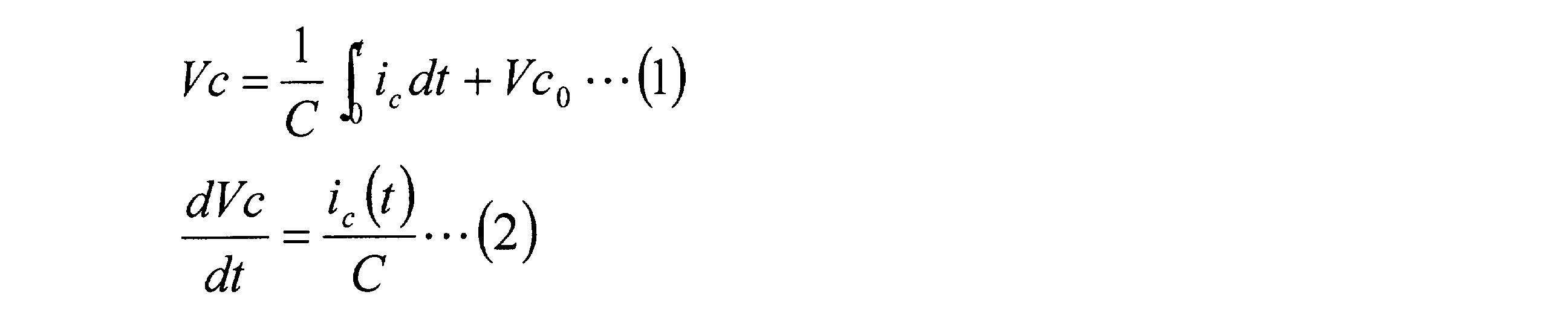
- the capacitor voltage Vc is the following equation (1)
- the voltage change rate dVc / dt of the capacitor voltage Vc is the following equation (2).
- C capacity
- I c capacitor current
- Vc 0 initial voltage of capacitor.
- the capacitor current i c in the normal operation has a value in a certain range depending on the load (inductance of the motor, etc.)
- the capacitor current i cs at the short circuit is limited mainly by the current due to the characteristics of the element and becomes large. Therefore, the relationship between the capacitor current i c in the normal operation and the capacitor current i cs in the short circuit is given by the following equation (3).
- a short circuit test is performed in advance in three types of short circuit modes (damage of element itself, false ignition, external short circuit), capacitor voltage V c is measured, It is conceivable to determine the threshold value of the rate of voltage change dV / dt of the short circuit failure.
- the short circuit in the inverter can be roughly divided into the following three types (1) (2) (3).
- (1) Failure of the element itself (2) In the case of erroneous ignition (3)
- the short circuit 1 shown in FIG. 3A is, for example, a case where the switching element S1 is damaged and the switching elements S2, S3, S4, S5, and S6 are erroneously turned on.
- the first and second capacitors C1 and C2 and the flying capacitors C3 and C4 as power supplies, a current flows which is determined by the active characteristics of the element and the impedance of the wiring.
- the emitter-collector of the switching element S1 is short-circuited with a conductor, and an ON signal is applied to the switching element S6 for measurement.
- the anode and the cathode of the diode D1 are short-circuited with a conductor, and an ON signal is applied to the switching element S2 (or S5) for measurement.
- the voltage change rate dV / dt of the flying capacitors C3 and C4 basically becomes different values.
- the switching element viewed as a broken element of (1) also receives an on signal simultaneously with the other switching elements, and measures the voltage change rate dV / dt.
- U phase-V phase short circuit For example, U phase switching elements S1, S2, S3 are turned on, V phase switching elements S4, S5, S6 are turned on, and U phase-V phase is shorted In this case, a short circuit current flows from the first and second capacitors C1 and C2 and the flying capacitor C3.
- the voltage change rate detectors 2a and 2b constantly calculate the voltage change rate dV / dt, and send out a short circuit fault signal to the controller 6 in the phase module 4 when the threshold is exceeded. At the same time, the value of the voltage change rate dV / dt is stored in a storage unit (not shown). Then, a shutoff signal is sent from the controller unit 6 to the drive circuit 7 to turn off the switching elements S1 to S8.
- a spike-like voltage drop occurs at the occurrence of a short circuit, and the voltage change rate dV / dt measures a large value in section A, but in terms of calculation of the voltage change rate dV / dt
- the voltage change rate dV / dt at A may or may not be ignored.
- a measurement value for example, a moving average value of voltage change rate dV / dt at each sampling is used.
- the controller common to each phase module since the controller common to each phase module is not used, short circuit detection / cut in a short time in the phase module 4 in which the short circuit occurs. Protection action can be performed.
- short circuit detection / cutoff protection operation can be performed in a short time after a short circuit occurs, the responsibility of the current change rate suppression reactors L1 and L2 can be reduced.
- the responsibility of the current change rate suppression reactors L1 and L2 can be reduced, the responsibility of the snubber circuits 1a and 1b can be relaxed.
- the present invention is applicable to any voltage type multi-level converter provided with a flying capacitor.
Landscapes
- Engineering & Computer Science (AREA)
- Power Engineering (AREA)
- Inverter Devices (AREA)
Abstract
各相ごとに設けられ、コンデンサC1,C2と異なる電圧が充電されたフライングキャパシタC3,C4に対して、フライングキャパシタC3,C4両端の電圧変化率を検出する電圧変化率検出部2a,2bを設け、前記フライングキャパシタC3,C4両端の電圧変化率が閾値を超えた場合、短絡として検出する。そして、短絡異常信号を各相のコントローラ部6に送信し、各スイッチング素子のドライブ回路7でゲート信号を遮断する。これにより、共通のコントローラと相モジュール内のコントローラ間の通信速度を高速化することなく、かつ、簡易な構成で、短絡故障に対する保護処理を行う。
Description
本発明は、フライングキャパシタを用いた電圧型マルチレベル変換器に関する。
近年、パワーデバイス(例えば、IGBT等:以下、スイッチング素子と称する)を用いた可変速駆動装置,電力変換装置においては、マルチレベル変換器が主流となりつつある。
図6は、従来の電圧型マルチレベル変換器の一例を示す図である。図6に示す電圧型マルチレベル変換器は、直流電圧源(図示省略)の正負極間に直列接続された第1,第2コンデンサC1,C2と、電流変化率抑制リアクトルL1,L2を有しサージ電圧を抑制するスナバ回路1a,1bと、電流変化率抑制リアクトルL1,L2における電流変化率di/dtを検出する電流変化率検出部3a,3bと、フライングキャパシタC3,C4を有する相モジュール4と、を備えている。図6では簡単化の為に相モジュール4は1相分のみ示している。
図6に示す電圧型マルチレベル変換器では、電流変化率検出部3a,3bから出力された電流変化率検出値di/dtが一定値以上の場合に相モジュール4内で短絡が生じたと判断し、共通のコントローラ(図示省略)を経由して相モジュール4内のコントローラ(図示省略)に短絡異常信号を送信する。その後、相モジュール4内のコントローラからスイッチング素子のドライブ回路にゲート遮断信号を送信して安全にゲート信号を遮断する。
装置の負荷には所定の電流波形があり、これに伴うフライングキャパシタの電流変化率di/dtは既知であるため予め基準値として設定しておき、この基準値と電流変化率検出部3a,3bの電流変化率検出値di/dtと比較することにより、短絡判断を行うことができる。
しかしながら、図6に示す電圧型マルチレベル変換器は、直流電圧源に接続された第1,第2コンデンサC1,C2および電流変化率抑制リアクトルL1,L2が各相モジュール4に対し共通であることから1箇所にのみ設けられている。そのため、短絡異常が発生した場合は電流変化率検出値di/dtは共通のコントローラを経由し、相モジュール4内のコントローラに短絡異常信号を送信する必要があった。その結果、共通のコントローラと相モジュール4内のコントローラ間の通信速度を高速化するか、或いは、さらに大きな電流変化率抑制リアクトルL1,L2やスナバ回路1a,1bを設けて短絡電流を抑制する必要があった。
以上示したようなことから、電圧型マルチレベル変換器において、共通のコントローラと相モジュール内のコントローラ間の通信速度を高速化することなく、かつ、簡易な構成で、短絡故障に対する保護処理を行うことが課題となる。
本発明は、前記従来の問題に鑑み、案出されたもので、その一態様は、直流電圧を複数の電圧レベルに変換した交流出力を生成する電圧型マルチレベル変換器であって、直流電圧源の両端子間に直列に接続された各相共通のコンデンサと、各相ごとに設けられ、前記コンデンサと異なる電圧が充電されるフライングキャパシタと、各相ごとに複数のスイッチング素子を有し、このスイッチング素子を選択的にON,OFF制御することにより、前記コンデンサおよびフライングキャパシタの電圧に基づいて複数の電圧レベルを選択的に出力する電圧選択回路と、前記フライングキャパシタ両端の電圧変化率を検出する電圧変化率検出部と、を備え、前記フライングキャパシタ両端の電圧変化率が閾値を超えた場合、短絡として検出することを特徴とする。
また、その一態様として、前記フライングキャパシタ両端の電圧変化率が閾値を超えた場合、短絡異常信号を相モジュール内のコントローラに出力することを特徴とする。
さらに、その一態様として、前記フライングキャパシタ両端の電圧変化率の値により、短絡の要因を特定することを特徴とする。
本発明によれば、電圧型マルチレベル変換器において、共通のコントローラと相モジュール内のコントローラ間の通信速度を高速化することなく、かつ、簡易な構成で、短絡故障に対する保護処理を行うことが可能となる。
本願発明は、フライングキャパシタを用いた電圧形マルチレベル変換器において、出力側の低インピーダンス短絡、突発的なスイッチング素子等の異常や、偶発的なドライブ回路の誤動作により生じる短絡故障等を検出し、故障範囲の拡大を防止するものである。
以下、本願発明に係る電圧型マルチレベル変換器における実施形態を図1~図5に基づいて詳述する。
[実施形態]
図1は、本実施形態における電圧型マルチレベル変換器の回路構成図であり、本実施形態では5レベルの電圧型電力変換装置を例にして説明する。図1に示すように、本実施形態における電圧型マルチレベル変換器は、直流電圧源(図示省略)の正負極端間に第1,第2コンデンサC1,C2を直列接続し、その第1,第2コンデンサC1,C2の共通接続点を出力端子Bとする。また、以下の説明では、直流電圧源の正極端をP、負極端をNとする。
図1は、本実施形態における電圧型マルチレベル変換器の回路構成図であり、本実施形態では5レベルの電圧型電力変換装置を例にして説明する。図1に示すように、本実施形態における電圧型マルチレベル変換器は、直流電圧源(図示省略)の正負極端間に第1,第2コンデンサC1,C2を直列接続し、その第1,第2コンデンサC1,C2の共通接続点を出力端子Bとする。また、以下の説明では、直流電圧源の正極端をP、負極端をNとする。
前記Pから第1スイッチング素子S1,フライングキャパシタC3を順次直列に接続する。前記Nから第6スイッチング素子,フライングキャパシタC4を順次直列接続する。また、フライングキャパシタC3とC4は直列に接続し、第1スイッチング素子S1,フライングキャパシタC3,C4,第6スイッチング素子S6で第1直列回路を構成する。
第2,第3,第4,第5スイッチング素子S2,S3,S4,S5を順次直列接続し、第2直列回路を構成する。前記第2スイッチング素子S2は第1スイッチング素子S1とフライングキャパシタC3との共通接続点に接続し、前記第5スイッチング素子S5は第6スイッチング素子S6とフライングキャパシタC4との共通接続点に接続する。ここで、第2直列回路の中点(第3,第4スイッチング素子S3,S4の共通接続点)を出力端子Aとする。また、第2,第3スイッチング素子S2,S3の共通接続点と、第4,第5スイッチング素子S4,S5の共通接続点と、の間に第1,第2ダイオードD1,D2を介挿し、第1,第2ダイオードD1,D2の共通接続点は、フライングキャパシタC3,C4の共通接続点と接続される。
また、出力端子BとフライングキャパシタC3,C4の共通接続点との間には、第7スイッチング素子S7と第8スイッチング素子S8が逆向きに直列接続される。前記第1~第8のスイッチング素子S1~S8で電圧選択回路が構成される。
また、符号1a,1bはスナバ回路であり、それぞれスナバダイオードD3,D4,D5,D6,スナバコンデンサC5,C6,帰還抵抗R1,R2,電流変化抑制リアクトルL1,L2を有している。
また、フライングキャパシタC3,C4には分圧抵抗R3,R4を介してフライングキャパシタ両端の電圧変化率dV/dtを検出する電圧変化率検出部2a,2bが設けられている。
本実施形態における電圧型マルチレベル変換器は、第1,第2コンデンサC1,C2の電圧が2E,フライングキャパシタC3,C4の電圧がEの時、各スイッチング素子のドライブ回路7において、前記スイッチング素子S1~S8を下記表1に示すモード1~7のスイッチングパターンに従ってオンオフ制御することにより、出力端子AB間に5レベルの電圧2E,E,0,-E,-2Eを出力できる。

ここで、表1のスイッチングパターンの各モード1~7と出力端子A,B間の電流IAの経路について説明する。
〈モード1〉
第1,第2,第3スイッチング素子S1,S2,S3がオン、第4,第5,第6,第7,第8スイッチング素子S4,S5,S6,S7,S8がオフとなり、電流IAは出力端子B→第1コンデンサC1→P→S1→S2→S3→出力端子Aの経路で流れる。出力端子AB間には第1コンデンサC1の負側→正側が接続され、出力端子A,B間の電圧は2Eとなる。
第1,第2,第3スイッチング素子S1,S2,S3がオン、第4,第5,第6,第7,第8スイッチング素子S4,S5,S6,S7,S8がオフとなり、電流IAは出力端子B→第1コンデンサC1→P→S1→S2→S3→出力端子Aの経路で流れる。出力端子AB間には第1コンデンサC1の負側→正側が接続され、出力端子A,B間の電圧は2Eとなる。
〈モード2〉
第1,第3,第4スイッチング素子S1,S3,S4がオン、第2,第5,第6,第7,第8スイッチング素子S2,S5,S6,S7,S8がオフとなり、電流IAは出力端子B→第1コンデンサC1→P→S1→フライングキャパシタC3→D1→S3→出力端子A(または、出力端子B→第1コンデンサC1→P→S1→フライングキャパシタC3→D2→S4→出力端子A)の経路で流れる。出力端子AB間には第1コンデンサC1の負側→正側→フライングキャパシタC3の正側→負側が直列に接続され、出力端子A,B間の電圧は2E-E=Eとなる。このモード2では電流IA>0のときフライングキャパシタC3は充電される。
第1,第3,第4スイッチング素子S1,S3,S4がオン、第2,第5,第6,第7,第8スイッチング素子S2,S5,S6,S7,S8がオフとなり、電流IAは出力端子B→第1コンデンサC1→P→S1→フライングキャパシタC3→D1→S3→出力端子A(または、出力端子B→第1コンデンサC1→P→S1→フライングキャパシタC3→D2→S4→出力端子A)の経路で流れる。出力端子AB間には第1コンデンサC1の負側→正側→フライングキャパシタC3の正側→負側が直列に接続され、出力端子A,B間の電圧は2E-E=Eとなる。このモード2では電流IA>0のときフライングキャパシタC3は充電される。
〈モード3〉
第2,第3,第7,第8スイッチング素子S2,S3,S7,S8がオン、第1,第4,第5,第6スイッチング素子S1,S4,S5,S6がオフとなり、電流IAは出力端子B→S7→S8→フライングキャパシタC3→S2→S3→出力端子Aの経路で流れる。出力端子AB間にはフライングキャパシタC3の負側→正側が接続され、出力端子A,B間の電圧はEとなる。このモード3では電流IA>0のときフライングキャパシタC3は充電される。
第2,第3,第7,第8スイッチング素子S2,S3,S7,S8がオン、第1,第4,第5,第6スイッチング素子S1,S4,S5,S6がオフとなり、電流IAは出力端子B→S7→S8→フライングキャパシタC3→S2→S3→出力端子Aの経路で流れる。出力端子AB間にはフライングキャパシタC3の負側→正側が接続され、出力端子A,B間の電圧はEとなる。このモード3では電流IA>0のときフライングキャパシタC3は充電される。
〈モード4〉
第3,第4,第7,第8スイッチング素子S3,S4,S7,S8がオン、第1,第2,第5,第6スイッチング素子S1,S2,S5,S6がオフとなり、電流は出力端子B→S7→S8→D1→S3→出力端子A(または、電流IAが負の時、出力端子B→S7→S8→D2→S4→出力端子A)の経路で流れる。出力端子AB間には第7,第8,第1スイッチング素子S7,S8,S1(または、電流IAが負の時は第7,第8,第2スイッチング素子S7,S8,S2)を介して直送され、出力端子AB間の電圧は0となる。
第3,第4,第7,第8スイッチング素子S3,S4,S7,S8がオン、第1,第2,第5,第6スイッチング素子S1,S2,S5,S6がオフとなり、電流は出力端子B→S7→S8→D1→S3→出力端子A(または、電流IAが負の時、出力端子B→S7→S8→D2→S4→出力端子A)の経路で流れる。出力端子AB間には第7,第8,第1スイッチング素子S7,S8,S1(または、電流IAが負の時は第7,第8,第2スイッチング素子S7,S8,S2)を介して直送され、出力端子AB間の電圧は0となる。
〈モード5〉
第4,第5,第7,第8スイッチング素子S4,S5,S7,S8がオン、第1,第2,第3,第6スイッチング素子S1,S2,S3,S6がオフとなり、電流IAは出力端子B→S7→S8→フライングキャパシタC4→S5→S4→出力端子Aの経路で流れる。出力端子AB間にはフライングキャパシタC4の正側→負側が直列に接続され、出力端子A,B間の電圧は-Eとなる。このモード5では電流IA>0のときフライングキャパシタC4は放電される。
第4,第5,第7,第8スイッチング素子S4,S5,S7,S8がオン、第1,第2,第3,第6スイッチング素子S1,S2,S3,S6がオフとなり、電流IAは出力端子B→S7→S8→フライングキャパシタC4→S5→S4→出力端子Aの経路で流れる。出力端子AB間にはフライングキャパシタC4の正側→負側が直列に接続され、出力端子A,B間の電圧は-Eとなる。このモード5では電流IA>0のときフライングキャパシタC4は放電される。
〈モード6〉
第3,第4,第6スイッチング素子S3,S4,S6がオン、第1,第2,第5,第7,第8スイッチング素子S1,S2,S5,S7,S8がオフとなり、電流IAは出力端子B→第2コンデンサC2→N→S6→フライングキャパシタC4→D1→S3→出力端子A(または、電流IAが負の時、出力端子B→第2コンデンサC2→N→S6→フライングキャパシタC4→D2→S4→出力端子A)の経路で流れる。出力端子AB間には第2コンデンサC2の正側→負側→フライングキャパシタC4の負側→正側が直列に接続され、出力端子A,B間の電圧は-2E+E=-Eとなる。このモード6では電流IA>0のときフライングキャパシタC4は充電される。
第3,第4,第6スイッチング素子S3,S4,S6がオン、第1,第2,第5,第7,第8スイッチング素子S1,S2,S5,S7,S8がオフとなり、電流IAは出力端子B→第2コンデンサC2→N→S6→フライングキャパシタC4→D1→S3→出力端子A(または、電流IAが負の時、出力端子B→第2コンデンサC2→N→S6→フライングキャパシタC4→D2→S4→出力端子A)の経路で流れる。出力端子AB間には第2コンデンサC2の正側→負側→フライングキャパシタC4の負側→正側が直列に接続され、出力端子A,B間の電圧は-2E+E=-Eとなる。このモード6では電流IA>0のときフライングキャパシタC4は充電される。
〈モード7〉
第4,第5,第6スイッチング素子S4,S5,S6がオン、第1,第2,第3,第7,第8スイッチング素子S1,S2,S3,S7,S8がオフとなり、電流IAは出力端子B→第2コンデンサC2→N→S6→S5→S4→出力端子Aの経路で流れる。出力端子AB間には第2コンデンサC2の正側→負側が接続され、出力端子A,B間の電圧は-2Eとなる。
第4,第5,第6スイッチング素子S4,S5,S6がオン、第1,第2,第3,第7,第8スイッチング素子S1,S2,S3,S7,S8がオフとなり、電流IAは出力端子B→第2コンデンサC2→N→S6→S5→S4→出力端子Aの経路で流れる。出力端子AB間には第2コンデンサC2の正側→負側が接続され、出力端子A,B間の電圧は-2Eとなる。
フライングキャパシタC3,C4の電圧は、出力電圧VABがEまたは-Eのとき充電または放電するスイッチングパターン(表1のMode2,3,5,6)を利用して制御することができる。すなわち、モード2とモード3の出力電圧はどちらもEであるが、フライングキャパシタC3を充電または放電が可能であるため、フライングキャパシタC3の電圧を調節することが可能である。同様に、モード5とモード6の出力電圧はどちらも-Eであるが、フライングキャパシタC4を充電または放電が可能であるため、フライングキャパシタC4の電圧を調節することが可能である。
次に、相モジュール4内の短絡故障に対する保護処理について説明する。
図6に示す従来例では各相共通の電流変化率抑制インダクタンスL1,L2における電流変化率di/dtを検出することにより相モジュール4の短絡を検出していたが、図1に示す本実施形態では相モジュール4内部のフライングキャパシタC3,C4における電圧変化率dV/dtの増加あるいは減少を検出することにより相モジュール4の短絡を検出している。
これにより、相モジュール4内において、短絡異常が発生した場合、電圧変化率検出部2a,2bの出力信号を、各相共通のコントローラを経由せずに、各相モジュール4内のコントローラ6とドライブ回路7のみを経由して、各スイッチング素子S1~S8のゲート信号を遮断することができる。また、フライングキャパシタC3,C4の電圧変化率dV/dtを検出する電圧変化率検出部2a,2bは電圧型マルチレベル変換器の制御のために元々設けられているため、そのまま共通流用することが可能である。
図3(a)に示す短絡回路(1)は、第1,第2コンデンサC1,C2とフライングキャパシタC3,C4が並列接続される例を示している。前述したように、フライングキャパシタC3,C4の電圧は第1,第2コンデンサC1,C2の電圧より低い電圧で充電されている。短絡回路(1)では、フライングキャパシタC3,C4の放電により電圧変化率dV/dtが減少する。
図3(b)に示す短絡回路(2)は、電圧源として第1,第2コンデンサC1,C2とフライングキャパシタC3,C4が直列接続される例を示している。短絡回路(2)では、第1,第2コンデンサC1,C2の電圧>フライングキャパシタC3,C4の電圧の場合であるため、フライングキャパシタC3,C4は第1,第2コンデンサC1,C2からの充電電流を受けて電圧変化率dV/dtが上昇する。
図3(c)に示す短絡回路(3)は、フライングキャパシタC3,C4のみ有する短絡回路例を示している。短絡回路3では、フライングキャパシタC3,C4の放電により電圧変化率dV/dtが減少する。
上記以外にも短絡経路はあるが、結果的に上記の短絡回路(1)~(3)に行き着く。
実際の第1,第2コンデンサC1,C2,フライングキャパシタC3,C4の等価回路を図4に示す。理想のコンデンサでは抵抗成分R=0,リアクトル成分L=0であるが、実際は、図4に示すように、リード線,接触抵抗の抵抗成分Rとリード線のリアクトル成分Lが寄生インピーダンスとして存在する。
矢印の方向(コンデンサから抵抗成分Rとリアクトル成分L方向)に急峻な電流が流れると、リアクトル成分LのところでLdi/dtおよび抵抗成分RのところでRdi/dtの電圧が生じ、リアクトル成分Lおよび抵抗成分R共にコンデンサC側に+極性が生じる。その結果、コンデンサCに対しての電圧降下が重畳される。
図5(a)は通常運転時、図5(b)は短絡時(放電の場合)の電流,電圧を示すタイムチャートである。図5(b)に示すように、短絡発生時に、スパイク状の電圧降下があるのは前記電圧降下が重畳されるためである。コンデンサ内部に寄生インピーダンスの抵抗成分R、リアクトル成分Lがない場合、コンデンサ電圧Vcは下記(1)式,コンデンサ電圧Vcの電圧変化率dVc/dtは下記(2)式となる。ただし、C:容量,Ic:コンデンサ電流,Vc0:キャパシタの初期電圧である。
通常運転時におけるコンデンサ電流icは、負荷(モータのインダクタンス等)により一定範囲の値であるが、短絡時のコンデンサ電流icsは主に素子の特性による電流で制約され大きくなる。そのため、通常運転時のコンデンサ電流icと短絡時のコンデンサ電流icsの関係は下記(3)式となる。

このため、通常運転時の電圧変化率dVc/dtと短絡時の電圧変化率dVcs/dtとの関係は下記(4)式となる。

このフライングキャパシタの電圧変化率dV/dtが所定の値を越えた場合を短絡異常として検出し、自己の相モジュール4内のコントローラ6を経由して、ドライブ回路7でゲート信号を遮断する。
短絡故障を判定するための閾値の決定方法としては、予め3種類の短絡モード(素子自体の破損,誤点弧,外部短絡)で短絡試験を行いコンデンサ電圧Vcを測定し、この値に基づいて短絡故障の電圧変化率dV/dtの閾値を決定しておく方法が考えられる。
以下、短絡モードの推定方法について説明する。
インバータでの短絡は大きく分けて以下(1)(2)(3)の3種類がある。
(1)素子自体の破損
(2)誤点弧による場合
(3)装置としての外部での短絡、例えばU相とV相を直に短絡する場合である。
(1)素子自体の破損
(2)誤点弧による場合
(3)装置としての外部での短絡、例えばU相とV相を直に短絡する場合である。
(1)(2)の場合は、素子劣化(製造不良含む)が主因である。2個同時に破損することは現実的にあっても、故障(破損)確率はワイブル分布に従うと考えてよいので、技術上1個ごとに破損すると考えてよい。短絡モードを検討する上で、同時に2個短絡を考える必要はなく、1個のみ破損するとして検討する。
まず、(1)の1素子破損した場合について説明する。
図3(a)の短絡回路1は、例えば、スイッチング素子S1が破損し、スイッチング素子S2,S3,S4,S5,S6がオンの誤動作した場合である。第1,第2コンデンサC1,C2,フライングキャパシタC3,C4を電源とし、素子の能動特性と配線のインピーダンスから決まる電流が流れる。(以下、短絡電流は素子の特性と配線のインピーダンスにより決まるので、記載は省略)
予め、電圧変化率dV/dtを測定する場合、スイッチング素子S1のみ素子のエミッタ-コレクタ間を導体で短絡しておき、スイッチング素子S2,S3,S4,S5,S6に全て同時にオン信号を入れて測定する。
予め、電圧変化率dV/dtを測定する場合、スイッチング素子S1のみ素子のエミッタ-コレクタ間を導体で短絡しておき、スイッチング素子S2,S3,S4,S5,S6に全て同時にオン信号を入れて測定する。
図3(b)の短絡回路2は2種類ある。
(i)P側の場合、スイッチング素子S1が破損(N側の場合、スイッチング素子S6が破損)し、スイッチング素子S7,S8にオンの誤動作信号が入った場合である。
予め、電圧変化率dV/dtを測定する場合、スイッチング素子S1(N側の場合、S6)のみ素子のエミッタ-コレクタ間を導体で短絡しておき、スイッチング素子S7,S8に全て同時にオン信号を入れて測定する。
(ii)スイッチング素子S1(またはS6)が破損し、スイッチング素子S6(またはS1)にオンの誤動作信号が入った場合である。
予め、電圧変化率dV/dtを測定する場合、スイッチング素子S1のみ素子のエミッタ-コレクタ間を導体で短絡しておき、スイッチング素子S6にオン信号を入れて測定する。
図3(c)の短絡回路3は2種類ある。
(i)ダイオードD1(または、D2)が破損し、スイッチング素子S2(またはS5)にオンの誤動作信号が入った場合である。
予め、電圧変化率dV/dtを測定する場合、ダイオードD1(またはD2)のアノード-カソード間を導体で短絡しておき、スイッチング素子S2(または、S5)にオン信号を入れて測定する。
(ii)スイッチング素子S2,S3,S4,S5のうち何れか1つが破損し、その他のスイッチング素子に同時にオンの誤動作信号が入った場合である。
予め、電圧変化率dV/dtを測定する場合、スイッチング素子S2(または、S3,S4,S5)のコレクタ-エミッタ間を導体で短絡しておき、スイッチング素子S2以外の素子に同時にオン信号を入れて測定する。
以上、短絡回路により、健全な素子数、配線のルートが異なるので、フライングキャパシタC3,C4の電圧変化率dV/dtは基本に異なる値となる。
(2)誤動作による短絡
予め、(1)の破損素子とみたスイッチング素子も他のスイッチング素子と同時にオンの信号を入れ、電圧変化率dV/dtを測定する。
予め、(1)の破損素子とみたスイッチング素子も他のスイッチング素子と同時にオンの信号を入れ、電圧変化率dV/dtを測定する。
(3)インバータ出力端子、U相-V相短絡
例えば、U相のスイッチング素子S1、S2、S3がオン、V相のスイッチング素子S4、S5、S6がオンで、U相-V相が短絡した場合、第1,第2コンデンサC1、C2,フライングキャパシタC3から短絡電流が流れる。
例えば、U相のスイッチング素子S1、S2、S3がオン、V相のスイッチング素子S4、S5、S6がオンで、U相-V相が短絡した場合、第1,第2コンデンサC1、C2,フライングキャパシタC3から短絡電流が流れる。

電圧変化率検出部2a,2bでは、常時、電圧変化率dV/dtを演算し、上記閾値を越えたとき短絡故障の信号を相モジュール4内のコントローラ部6に送出する。同時に、電圧変化率dV/dtの値を記憶部(図示省略)に保管する。そして、コントローラ部6からドライブ回路7に遮断信号が送出され、スイッチング素子S1~S8をオフする。
図5(b)に示すように、短絡発生時にスパイク状の電圧降下が発生し、区間Aにおいて電圧変化率dV/dtは大きな値を測定するが、電圧変化率dV/dtの演算上この区間Aにおける電圧変化率dV/dtを無視しても、無視しなくてもよい。測定値としては、例えば、サンプリングごとの電圧変化率dV/dtの移動平均値を使用する。
また、短絡故障したときに測定された電圧変化率dV/dtの値に基づいて、3種類(出力側の低インピーダンス短絡、突発的なスイッチング素子等の異常や,偶発的なドライブ回路の誤動作)の短絡モードのうちどの短絡モードであるかを推定することができる。
以上示したように、本実施形態における電圧型マルチレベル変換器によれば、各相モジュール共通のコントローラを経由することがないため、短絡が生じた相モジュール4内で短時間に短絡検出・遮断の保護動作を行うことができる。また、短絡が生じてから短時間に短絡検出・遮断の保護動作ができるため、電流変化率抑制リアクトルL1,L2の責務を軽減することができる。さらに、電流変化率抑制リアクトルL1,L2の責務を軽減できるため、スナバ回路1a,1bの責務を緩和することが可能となる。
また、共通のコントローラと相モジュール4内のコントローラ部6間の通信速度を高速化する必要がない。
以上、本発明において、記載された具体例に対してのみ詳細に説明したが、本発明の技術思想の範囲で多彩な変形および修正が可能であることは、当業者にとって明白なことであり、このような変形および修正が特許請求の範囲に属することは当然のことである。
例えば、実施形態において5レベルの電力変換装置について説明したが、本願発明は、フライングキャパシタを備えた電圧型マルチレベル変換器であれば適用可能である。
Claims (3)
- 直流電圧を複数の電圧レベルに変換した交流出力を生成する電圧型マルチレベル変換器であって、
直流電圧源の両端子間に直列に接続された各相共通のコンデンサと、
各相ごとに設けられ、前記コンデンサと異なる電圧が充電されるフライングキャパシタと、
各相ごとに複数のスイッチング素子を有し、このスイッチング素子を選択的にON,OFF制御することにより、前記コンデンサおよびフライングキャパシタの電圧に基づいて複数の電圧レベルを選択的に出力する電圧選択回路と、
前記フライングキャパシタ両端の電圧変化率を検出する電圧変化率検出部と、
を備え、
前記フライングキャパシタ両端の電圧変化率が閾値を超えた場合、短絡として検出する電圧型マルチレベル変換器。 - 前記フライングキャパシタ両端の電圧変化率が閾値を超えた場合、短絡異常信号を相モジュール内のコントローラに出力する請求項1記載の電圧型マルチレベル変換器。
- 前記フライングキャパシタ両端の電圧変化率の値により、短絡の要因を特定する請求項1または2記載の電圧型マルチレベル変換器。
Applications Claiming Priority (2)
| Application Number | Priority Date | Filing Date | Title |
|---|---|---|---|
| JP2013170939A JP5910584B2 (ja) | 2013-08-21 | 2013-08-21 | 電圧型マルチレベル変換器 |
| JP2013-170939 | 2013-08-21 |
Publications (1)
| Publication Number | Publication Date |
|---|---|
| WO2015025860A1 true WO2015025860A1 (ja) | 2015-02-26 |
Family
ID=52483633
Family Applications (1)
| Application Number | Title | Priority Date | Filing Date |
|---|---|---|---|
| PCT/JP2014/071699 Ceased WO2015025860A1 (ja) | 2013-08-21 | 2014-08-20 | 電圧型マルチレベル変換器 |
Country Status (2)
| Country | Link |
|---|---|
| JP (1) | JP5910584B2 (ja) |
| WO (1) | WO2015025860A1 (ja) |
Cited By (7)
| Publication number | Priority date | Publication date | Assignee | Title |
|---|---|---|---|---|
| CN105305864A (zh) * | 2015-11-06 | 2016-02-03 | 国家电网公司 | 一种基于谐振分流回路的换相装置及其实现方法 |
| CN106505899A (zh) * | 2016-11-11 | 2017-03-15 | 清华大学 | 中点箝位三电平单极电流模块 |
| EP3267572A4 (en) * | 2015-03-05 | 2018-10-31 | Sumitomo Electric Industries, Ltd. | Conversion device |
| CN110187209A (zh) * | 2019-06-04 | 2019-08-30 | 长沙晟道电气科技有限公司 | 模块化多电平变换器子模块故障检测方法、系统及介质 |
| JP2020089240A (ja) * | 2018-11-30 | 2020-06-04 | パナソニックIpマネジメント株式会社 | 電力変換装置、制御方法、及びプログラム |
| CN113555854A (zh) * | 2020-04-24 | 2021-10-26 | 台达电子企业管理(上海)有限公司 | 用于飞跨电容变换器的短路电流抑制电路与具有其的储能系统 |
| CN117220476A (zh) * | 2023-11-07 | 2023-12-12 | 深圳市力生美半导体股份有限公司 | 开关电源供电控制电路及供电控制方法 |
Families Citing this family (1)
| Publication number | Priority date | Publication date | Assignee | Title |
|---|---|---|---|---|
| EP4148964A1 (en) | 2021-09-14 | 2023-03-15 | ABB E-mobility B.V. | A method and a device for compensating a faulty switch in a multi-level flying capacitor converter |
Citations (5)
| Publication number | Priority date | Publication date | Assignee | Title |
|---|---|---|---|---|
| JPH07231674A (ja) * | 1994-02-22 | 1995-08-29 | Hitachi Ltd | 自己消弧半導体素子を用いたインバータ装置の制御方法 |
| JPH09205779A (ja) * | 1996-01-25 | 1997-08-05 | Hitachi Ltd | 電力変換装置 |
| JP2007184999A (ja) * | 2005-12-29 | 2007-07-19 | Toshiba Mitsubishi-Electric Industrial System Corp | 電力変換装置 |
| JP2008154420A (ja) * | 2006-12-20 | 2008-07-03 | Toshiba Mitsubishi-Electric Industrial System Corp | 電力変換装置 |
| JP2013146117A (ja) * | 2012-01-13 | 2013-07-25 | Fuji Electric Co Ltd | マルチレベル電力変換回路 |
Family Cites Families (2)
| Publication number | Priority date | Publication date | Assignee | Title |
|---|---|---|---|---|
| JP4120329B2 (ja) * | 2002-09-19 | 2008-07-16 | 富士電機デバイステクノロジー株式会社 | 電圧駆動型半導体素子のゲート駆動装置 |
| JP5056405B2 (ja) * | 2007-12-26 | 2012-10-24 | トヨタ自動車株式会社 | スイッチング装置 |
-
2013
- 2013-08-21 JP JP2013170939A patent/JP5910584B2/ja active Active
-
2014
- 2014-08-20 WO PCT/JP2014/071699 patent/WO2015025860A1/ja not_active Ceased
Patent Citations (5)
| Publication number | Priority date | Publication date | Assignee | Title |
|---|---|---|---|---|
| JPH07231674A (ja) * | 1994-02-22 | 1995-08-29 | Hitachi Ltd | 自己消弧半導体素子を用いたインバータ装置の制御方法 |
| JPH09205779A (ja) * | 1996-01-25 | 1997-08-05 | Hitachi Ltd | 電力変換装置 |
| JP2007184999A (ja) * | 2005-12-29 | 2007-07-19 | Toshiba Mitsubishi-Electric Industrial System Corp | 電力変換装置 |
| JP2008154420A (ja) * | 2006-12-20 | 2008-07-03 | Toshiba Mitsubishi-Electric Industrial System Corp | 電力変換装置 |
| JP2013146117A (ja) * | 2012-01-13 | 2013-07-25 | Fuji Electric Co Ltd | マルチレベル電力変換回路 |
Cited By (11)
| Publication number | Priority date | Publication date | Assignee | Title |
|---|---|---|---|---|
| EP3267572A4 (en) * | 2015-03-05 | 2018-10-31 | Sumitomo Electric Industries, Ltd. | Conversion device |
| CN105305864A (zh) * | 2015-11-06 | 2016-02-03 | 国家电网公司 | 一种基于谐振分流回路的换相装置及其实现方法 |
| CN105305864B (zh) * | 2015-11-06 | 2017-12-19 | 国家电网公司 | 一种基于谐振分流回路的换相装置及其实现方法 |
| CN106505899A (zh) * | 2016-11-11 | 2017-03-15 | 清华大学 | 中点箝位三电平单极电流模块 |
| JP2020089240A (ja) * | 2018-11-30 | 2020-06-04 | パナソニックIpマネジメント株式会社 | 電力変換装置、制御方法、及びプログラム |
| JP7108932B2 (ja) | 2018-11-30 | 2022-07-29 | パナソニックIpマネジメント株式会社 | 電力変換装置、制御方法、及びプログラム |
| CN110187209A (zh) * | 2019-06-04 | 2019-08-30 | 长沙晟道电气科技有限公司 | 模块化多电平变换器子模块故障检测方法、系统及介质 |
| CN110187209B (zh) * | 2019-06-04 | 2021-04-09 | 长沙晟道电气科技有限公司 | 模块化多电平变换器子模块故障检测方法、系统及介质 |
| CN113555854A (zh) * | 2020-04-24 | 2021-10-26 | 台达电子企业管理(上海)有限公司 | 用于飞跨电容变换器的短路电流抑制电路与具有其的储能系统 |
| CN117220476A (zh) * | 2023-11-07 | 2023-12-12 | 深圳市力生美半导体股份有限公司 | 开关电源供电控制电路及供电控制方法 |
| CN117220476B (zh) * | 2023-11-07 | 2024-02-27 | 深圳市力生美半导体股份有限公司 | 开关电源供电控制电路及供电控制方法 |
Also Published As
| Publication number | Publication date |
|---|---|
| JP2015042044A (ja) | 2015-03-02 |
| JP5910584B2 (ja) | 2016-04-27 |
Similar Documents
| Publication | Publication Date | Title |
|---|---|---|
| WO2015025860A1 (ja) | 電圧型マルチレベル変換器 | |
| US11799285B2 (en) | Method for starting photovoltaic rapid shutdown system, application apparatus and system | |
| US11320481B2 (en) | High voltage interlock circuit and detection method | |
| CN104795973B (zh) | 半导体驱动装置和使用该半导体驱动装置的电力变换装置 | |
| US10468972B2 (en) | Power converter including a plurality of converter cells connected in multiple series | |
| US9059709B2 (en) | Gate drive circuit for transistor | |
| US11563370B2 (en) | Protection scheme for power converters utilizing cascaded bipolar and unipolar power semiconductor devices | |
| US7489487B2 (en) | Multi-level power converter | |
| AU2012231405A1 (en) | System for detecting a failure associated with an inverter or associated machine | |
| US9030853B2 (en) | Power conversion equipment having a capacitor failure detecting circuit | |
| CN101291114A (zh) | 电力转换装置 | |
| CN103856082A (zh) | 一种整流器电路及一种控制直流母线中电流的方法 | |
| CN104218531A (zh) | 短路保护电路及其短路保护方法 | |
| CN217406179U (zh) | 一种直流并联系统、功率变换器的保护电路 | |
| JP5661414B2 (ja) | 電源装置 | |
| CN107390079B (zh) | 变流器、撬棒电路及其状态检测方法和控制方法 | |
| US6618235B1 (en) | Snubber circuit | |
| JP4773172B2 (ja) | 電力用スイッチング素子の電圧検出方法及びこれを用いた電力変換装置 | |
| CN104953805A (zh) | 管理变频器中功率单元的方法和设备 | |
| WO2021168907A1 (zh) | 一种伺服驱动器及其缓冲回路保护电路 | |
| JP2015029397A (ja) | 半導体電力変換装置 | |
| US20240072635A1 (en) | Gate drive circuit and power conversion device | |
| CN109991466A (zh) | 检测装置,保护系统及保护方法 | |
| JP7632883B2 (ja) | 半導体モジュールの過電流検出装置及びそれを用いた半導体モジュール、半導体モジュールの過電流検出方法 | |
| US20250237708A1 (en) | Fault Detection And Processing Method And Apparatus For Uninterruptible Power Supply, And Controller |
Legal Events
| Date | Code | Title | Description |
|---|---|---|---|
| 121 | Ep: the epo has been informed by wipo that ep was designated in this application |
Ref document number: 14837648 Country of ref document: EP Kind code of ref document: A1 |
|
| NENP | Non-entry into the national phase |
Ref country code: DE |
|
| 122 | Ep: pct application non-entry in european phase |
Ref document number: 14837648 Country of ref document: EP Kind code of ref document: A1 |