EP4148964A1 - A method and a device for compensating a faulty switch in a multi-level flying capacitor converter - Google Patents
A method and a device for compensating a faulty switch in a multi-level flying capacitor converter Download PDFInfo
- Publication number
- EP4148964A1 EP4148964A1 EP21196669.2A EP21196669A EP4148964A1 EP 4148964 A1 EP4148964 A1 EP 4148964A1 EP 21196669 A EP21196669 A EP 21196669A EP 4148964 A1 EP4148964 A1 EP 4148964A1
- Authority
- EP
- European Patent Office
- Prior art keywords
- converter
- level
- switch
- faulty
- capacitor
- Prior art date
- Legal status (The legal status is an assumption and is not a legal conclusion. Google has not performed a legal analysis and makes no representation as to the accuracy of the status listed.)
- Pending
Links
- 239000003990 capacitor Substances 0.000 title claims abstract description 130
- 238000000034 method Methods 0.000 title claims abstract description 29
- 238000007599 discharging Methods 0.000 claims abstract description 10
- 239000013598 vector Substances 0.000 claims description 14
- 238000004590 computer program Methods 0.000 claims description 5
- 238000004146 energy storage Methods 0.000 claims description 2
- 239000004065 semiconductor Substances 0.000 description 8
- 238000005259 measurement Methods 0.000 description 7
- 238000001514 detection method Methods 0.000 description 5
- 239000000969 carrier Substances 0.000 description 2
- 238000006243 chemical reaction Methods 0.000 description 2
- 238000002405 diagnostic procedure Methods 0.000 description 2
- 238000010586 diagram Methods 0.000 description 2
- 230000005669 field effect Effects 0.000 description 2
- 230000010363 phase shift Effects 0.000 description 2
- 238000012360 testing method Methods 0.000 description 2
- 230000003542 behavioural effect Effects 0.000 description 1
- 238000005352 clarification Methods 0.000 description 1
- 230000001351 cycling effect Effects 0.000 description 1
- 230000006378 damage Effects 0.000 description 1
- 230000001419 dependent effect Effects 0.000 description 1
- 238000012423 maintenance Methods 0.000 description 1
- 238000013021 overheating Methods 0.000 description 1
- 238000011144 upstream manufacturing Methods 0.000 description 1
- 239000013585 weight reducing agent Substances 0.000 description 1
Images


Classifications
-
- H—ELECTRICITY
- H02—GENERATION; CONVERSION OR DISTRIBUTION OF ELECTRIC POWER
- H02M—APPARATUS FOR CONVERSION BETWEEN AC AND AC, BETWEEN AC AND DC, OR BETWEEN DC AND DC, AND FOR USE WITH MAINS OR SIMILAR POWER SUPPLY SYSTEMS; CONVERSION OF DC OR AC INPUT POWER INTO SURGE OUTPUT POWER; CONTROL OR REGULATION THEREOF
- H02M1/00—Details of apparatus for conversion
- H02M1/32—Means for protecting converters other than automatic disconnection
- H02M1/322—Means for rapidly discharging a capacitor of the converter for protecting electrical components or for preventing electrical shock
-
- H—ELECTRICITY
- H02—GENERATION; CONVERSION OR DISTRIBUTION OF ELECTRIC POWER
- H02M—APPARATUS FOR CONVERSION BETWEEN AC AND AC, BETWEEN AC AND DC, OR BETWEEN DC AND DC, AND FOR USE WITH MAINS OR SIMILAR POWER SUPPLY SYSTEMS; CONVERSION OF DC OR AC INPUT POWER INTO SURGE OUTPUT POWER; CONTROL OR REGULATION THEREOF
- H02M1/00—Details of apparatus for conversion
- H02M1/32—Means for protecting converters other than automatic disconnection
- H02M1/325—Means for protecting converters other than automatic disconnection with means for allowing continuous operation despite a fault, i.e. fault tolerant converters
-
- H—ELECTRICITY
- H02—GENERATION; CONVERSION OR DISTRIBUTION OF ELECTRIC POWER
- H02M—APPARATUS FOR CONVERSION BETWEEN AC AND AC, BETWEEN AC AND DC, OR BETWEEN DC AND DC, AND FOR USE WITH MAINS OR SIMILAR POWER SUPPLY SYSTEMS; CONVERSION OF DC OR AC INPUT POWER INTO SURGE OUTPUT POWER; CONTROL OR REGULATION THEREOF
- H02M1/00—Details of apparatus for conversion
- H02M1/36—Means for starting or stopping converters
-
- H—ELECTRICITY
- H02—GENERATION; CONVERSION OR DISTRIBUTION OF ELECTRIC POWER
- H02M—APPARATUS FOR CONVERSION BETWEEN AC AND AC, BETWEEN AC AND DC, OR BETWEEN DC AND DC, AND FOR USE WITH MAINS OR SIMILAR POWER SUPPLY SYSTEMS; CONVERSION OF DC OR AC INPUT POWER INTO SURGE OUTPUT POWER; CONTROL OR REGULATION THEREOF
- H02M7/00—Conversion of ac power input into dc power output; Conversion of dc power input into ac power output
- H02M7/42—Conversion of dc power input into ac power output without possibility of reversal
- H02M7/44—Conversion of dc power input into ac power output without possibility of reversal by static converters
- H02M7/48—Conversion of dc power input into ac power output without possibility of reversal by static converters using discharge tubes with control electrode or semiconductor devices with control electrode
- H02M7/483—Converters with outputs that each can have more than two voltages levels
- H02M7/4837—Flying capacitor converters
-
- Y—GENERAL TAGGING OF NEW TECHNOLOGICAL DEVELOPMENTS; GENERAL TAGGING OF CROSS-SECTIONAL TECHNOLOGIES SPANNING OVER SEVERAL SECTIONS OF THE IPC; TECHNICAL SUBJECTS COVERED BY FORMER USPC CROSS-REFERENCE ART COLLECTIONS [XRACs] AND DIGESTS
- Y02—TECHNOLOGIES OR APPLICATIONS FOR MITIGATION OR ADAPTATION AGAINST CLIMATE CHANGE
- Y02E—REDUCTION OF GREENHOUSE GAS [GHG] EMISSIONS, RELATED TO ENERGY GENERATION, TRANSMISSION OR DISTRIBUTION
- Y02E10/00—Energy generation through renewable energy sources
- Y02E10/50—Photovoltaic [PV] energy
- Y02E10/56—Power conversion systems, e.g. maximum power point trackers
Definitions
- the invention relates to the field of multi-level flying capacitor converter, particularly for compensating a faulty switch in a multi-level flying capacitor converter.
- the invention further relates to a method, to a use, to a program element, and to a computer-readable storage medium.
- a converter that uses a flying capacitor multilevel topology may bring many benefits, for instance a significant converter weight reduction. Hence, it is desirable to increase the availability of the multi-level flying capacitor converter.
- One aspect relates to a method for compensating a faulty switch in a multi-level flying capacitor converter, wherein each converter level of the multi-level converter comprises a converter capacitor, arranged in parallel to an input of the multi-level converter, a first converter switch and a second converter switch, arranged between a first end or a second end of the converter capacitor respectively, and a first bypass switch and a second bypass switch, arranged in parallel to the respective first converter switch and the respective second converter switch.
- the method comprising the steps of:
- the multi-level flying capacitor converter converts an input DC signal into an AC output signal.
- the AC output signal may have one phase or more phases, for example three phases.
- Embodiments of the multi-level converter may be designed for low voltages, e.g. 5 V, other embodiments may be designed for low voltages, e.g. in a voltage range of 230 V, 1 kV, and/or other voltage range, and another embodiments be designed for variable voltages.
- the power transformed by the multi-level converter may range between a few watts, up to a MW range.
- the multi-level flying capacitor converter basically comprises a plurality of "levels", each of these levels comprising a “flying capacitor” or converter capacitor, which is charged by one or two switches upstream and discharged by the one or two switches downstream.
- the "flying capacitor” or converter capacitor is arranged in parallel to the input of the multi-level converter.
- Each of the one or two switches - i.e. the first converter switch and, optionally, the second converter switch - is arranged between a first end or a second end of the converter capacitor respectively.
- the first bypass switch and the (optional, if there is a second converter switch) second bypass switch are arranged in parallel to the respective first converter switch and the respective second converter switch.
- the converter switch may be implemented by a semiconductor, for instance by a FET, e.g. a MOSFET (metal-oxide-semiconductor field-effect transistor), or an IGBT (insulated gate bi-polar junction transistor).
- a capacitor may be arranged in parallel to the converter switch, to improve the electrical behaviour.
- the converter capacitor which would be directly connected to the one or two switches of the last level, may be lacking.
- a faulty converter level is a level of the multi-level converter, which has a faulty first converter switch and/or a faulty second converter switch. For most multi-level converters, it may be a rare event that both converter switch become faulty at the same time. Detecting a faulty converter level may include to identify the faulty converter switch and/or the kind of fault, i.e. an open-circuit failure or short circuit failure. Once an error - i.e. the faulty converter level - is detected, the system may be stopped and then disconnected from the grid (e.g. AC grid, or another (rectified) DC input voltage) in order to protect the devices from over-voltages and/or over-currents.
- the grid e.g. AC grid, or another (rectified) DC input voltage
- all capacitors arranged in parallel to the input of the multi-level converter are discharged.
- the term "all capacitors" may - besides the converter capacitors - also comprise more capacitors, e.g. also one or more input capacitor(s) and/or one or more output capacitor(s).
- the discharging may, for instance, be performed by closing all the bypass switches, and/or by other means.
- the discharging may be a complete or a partial discharging, at least to a charging-level where a safe bypassing of the faulty switching cell by bypass switches is possible.
- the bypass switches After the discharging, all switches of the faulty switching cell are shorted by the bypass switches, by closing the first bypass switch and the (optional) second bypass switch of the faulty converter level. Shorting the bypass switches reduces one level of the multilevel converter, i.e. it makes the n-level converter an (n-1)-level converter.
- the modulation of the converter switches of the other (or "remaining") converter levels has to be adapted.
- the adapting of the modulation may comprise removing the carrier for the faulty switching cell, and adjusting the phase shift between the remaining carriers, i.e. of the remaining levels. With this adapted modulation, the multi-level converter may be restarted. The restarting may be followed by continuing to run the multi-level converter.
- This method increases the availability of the multi-level flying capacitor converter significantly, because a faulty switch does not immediately lead to a fail of the multilevel converter.
- a multi-level converter which may be selected for behavioural reasons, may additionally bring the benefit of higher availability and/or reliability.
- the multi-level converters may - depending on the number of levels - even tolerate a double failure or even a failure of a higher degree.
- the method further comprises the step of conducting an initial check of the multi-level converter before continuing to run the multi-level converter.
- the initial check may comprise to check the functionalities in the converter system, for instance to check - after the capacitors have been charged again -if their voltages are balanced.
- a detecting of the faulty converter level may be performed, wherein the faulty converter level comprises the first converter switch and/or the second converter switch being faulty.
- the converter switch may have a short-circuit error or an open-circuit error.
- the identifying the converter switch having an open-circuit error comprises to measure a maximum voltage at one of the converter capacitors, and/or to apply a sequence of switching vectors to the switches of the multi-level flying capacitor converter. Details are given below.
- the identifying the converter switch having a short-circuit error comprises to measure a zero difference voltage between two of the converter capacitors. Details are given below.
- An aspect relates to a multi-level flying capacitor converter for DC/AC converting, wherein each converter level of the multi-level converter comprises:
- the multi-level converter comprises between 2 and 10 converter levels, particularly between 3 and 6 converter levels. More levels may lead to a smoother behaviour of the multi-level converter. However, additional steps may also increase the costs for the converter. Hence, it turned out that a good compromise may be to use between 3 and 6 converter levels, for instance 4 or 5 converter levels. In combination with the architecture described above and/or below, this also provides sufficient "reserve” in case of a single failure, or even of a failure of a higher degree.
- the multi-level converter further comprises an input capacitor and/or an output low-pass.
- the output low-pass may comprise an inductor arranged in series to the output and a capacitor arranged in parallel to the output, e.g. after the inductor. This may contribute to less distortion or harmonic distortion of the output signal of the multi-level converter.
- An aspect relates to a computer program product comprising instructions, which, when the program is executed by a control unit, cause the control unit to carry out the method as described above and/or below.
- An aspect relates to a computer-readable storage medium where a computer program or a computer program product as described above is stored on.
- An aspect relates to a use of a multi-level converter described above and/or below or a method described above and/or below for a PV (photovoltaic) inverter, UPS (uninterrupted power supply) systems, high-speed drives or motors, BESS (battery energy storage system), EV (electric vehicle) charging, and/or further DC/AC converting systems.
- PV photovoltaic
- UPS uninterrupted power supply
- BESS battery energy storage system
- EV electric vehicle charging
- DC/AC converting systems DC/AC converting systems.
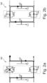
- Fig. 1 shows schematically an example of a flying capacitor converter 100, particularly a 5-level flying capacitor converter comprising 4 flying capacitor cells.
- the converter shown depicts MOSFETs (metal-oxide-semiconductor field-effect transistors) as switches 122, 124, 142, 144, 162, 164, 182, 184; however, also other kind of switches may be used, for instance other types of FETs and/or bipolar transistors.
- MOSFETs metal-oxide-semiconductor field-effect transistors
- Fig. 2a shows schematically an example of an open-circuit failure in an example cell 140.
- a converter switch 142 and/or 144 may fail by itself, and/or it may be possible that a gate drive circuit of the switch has failed. Either case may lead to a possible situation that the switch has failed in open circuit and cannot be turned-on again.
- a direction of a sinusoidal phase current i L (see, e.g., Fig. 1 ) is considered positive (i L > 0) and towards the grid.
- i L ⁇ 0 In the negative half-cycle (i L ⁇ 0), this direction reverses and the phase current is flowing towards the converter.
- i L is assumed being in its positive half-cycle (i L > 0), so flowing towards the grid.
- switch 142 fails in open, then in the next few switching cycles, the flying capacitor 127 can only be charged, while 147 can only be discharged, since the charging current would be blocked by the open-circuited switch 142. Accordingly, the voltage difference between V cf1 and V cf2 is increasing rapidly.
- the other capacitor voltages may also adapt, but much slower than the two flying capacitors on either side of the failed switch.
- switch 142 fails while the current i L is in the negative half cycle (i L ⁇ 0), flowing towards the converter, then the converter operation is not affected, since the diode of the switch 142 takes over the operation. Under such a condition, an open circuit failure of the switch 142 cannot be detected immediately. One would have to wait until the positive half-cycle arrives.
- V mid-out +1/4 V dc
- Fig. 2b shows schematically an example of a short-circuit failure in an example cell 140.
- a switch can fail by itself, and/or it may be possible that a gate drive circuit of the switch has failed. Either case may lead to a possible situation that the switch has failed in short circuit.
- the direction of the sinusoidal phase current i L is considered positive (i L > 0), and towards the grid if its flowing in the direction as shown in Fig. 1 .
- the negative half-cycle i L ⁇ 0
- this direction reverses and the phase current is flowing towards the converter.
- the system changes from a five to a four-level system and therefore higher distortions in the output current will be observed due to the increased switched voltage or reduced voltage-levels at the converter's output.
- this may not be the case and the overcurrent in the switches at the instant of fault could cause overheating to such an extent that switch will be destroyed and the system can no longer operate normally.
- the cases of inverter and rectifier operation may not needed to be separated.
- a flying capacitor converter As discussed above, there are two error cases considered for a flying capacitor converter: a device failing in open circuit or in short circuit.
- an n-level flying capacitor converter system is considered, with the capacitor 127 at the highest voltage V cf1 , and C f(n-2) with the lowest flying capacitor voltage, V cf(n-2) .
- the DC-link capacitors 112, 114 are is also considered as a flying capacitor with voltage V DC .
- the capacitance C f(n-1) ⁇ .
- the system has (n-1) switching cells, whereas - for example - switching cell 140 is located between capacitors 127 and 147.
- the measurements of the flying capacitor voltages, the phase currents and the AC-side filter capacitor voltages can be used, which usually are measured anyway for closed loop control of the converter. Alternatively, the voltages across the switches could directly be measured, although this may result in significantly increased measurement effort and cost in terms of hardware.
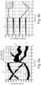
- Fig. 4a and 4b show schematically an example of an inverter operation of a 5-level flying capacitor system 100.
- Fig. 4a shows inductor currents
- Fig. 4b shows capacitor voltages when an open-circuit error in the high side device 142 of switching cell 140 in phase a occurs during the positive half-cycle of i (L,a) .
- Fig. 5a and 5b show schematically an example of another inverter operation of a 5-level flying capacitor system 100.
- Fig. 5a shows inductor currents
- Fig. 5b shows capacitor voltages when an open-circuit error in the high side device of switching cell 140 in phase a occurs during the negative half-cycle of i (L,a) .
- the area of about 5.5 ms indicates the time range when the error could have happened.
- the phase current can be used to detect if a device has failed in an open-circuit and cannot be turned on again.
- Fig. 4a, 4b , 5a and 5b depict the situation when the high side device switch 142 (see, e.g., Fig. 1 ) in switching cell 140 of the phase, say phase A of a 3-phase inverter/rectifier, is failing.
- the phase current can be used to detect an open circuit fault in the switch, for example by comparing it to a reference band as illustrated with dashed lines.
- other measurements can be used to detect an error.
- the deviation of the capacitor voltages may be too slow to allow a speedy identification of the switch failure. In the considered example this is especially the case if the open-circuit with high side device switch 142 fault happens during the negative half-cycle of the current (see Figs. 4a - 5b ). Therefore, information from the current sensor may be used to instead.
- Fig. 6a and 6b show schematically an example of a rectifier operation of a 5-level flying capacitor system.
- Fig. 6a shows inductor currents
- Fig. 6b shows capacitor voltages when an open-circuit error in the high side device of switching cell 140 in phase A occurs during the positive half-cycle of i (L,a) .
- Fig. 7a and 7b show schematically an example of another rectifier operation of a 5-level flying capacitor system.
- Fig. 7a shows inductor currents
- Fig. 7b shows capacitor voltages when an open-circuit error in the high side device of switching cell 140 in phase a occurs during the negative half-cycle of i (L,a) .
- the area of about 5.5 ms indicates the time range when the error could have happened.
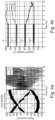
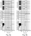
- Fig. 8a and 8b show schematically examples of test vectors to identify a faulty switching cell.
- Fig. 8a shows a sequence of switching vectors
- Fig. 8b shows two switching vectors.
- the deviation on the flying capacitor voltage may, in some cases, not be significant enough.
- a diagnostic procedure might be necessary in order to identify the faulty switching cell.
- a sequence of switching vectors can be applied on the faulty phase or all phases after disconnecting the system from the grid. Two examples of such switching vector sequences are shown next to further explain the idea.
- Example 1 In Fig. 8a at t 0 , after an open circuit fault in switch 162 has occurred. This fault is detected, and the converter is turned off and disconnected from the grid. To identify where exactly the fault has developed, a sequence of switching vectors is applied by cycling the phase voltage from a maximum possible negative voltage level to the maximum possible positive voltage level. The faulty switching cell can be found by either measuring the flying capacitor voltage or the converter output voltage. For example, at t 3 , switch 162 should be switched on but it stays open due to the fault. Thus, no change in the difference of flying capacitor voltages V cf nor any change in the phase voltage is seen and thus, the failed device is identified.
- Example 2 In Fig. 8b at t 0 , after an open circuit fault in switch 162 has occurred. This fault is detected, and the converter is turned off and disconnected from the grid. To identify where exactly the fault has developed, a sequence of switching vectors is applied, first all low side devices are turned on at t 1 , afterwards at t 2 all high side devices are turned on. Since switch 162 cannot be turned on again, the voltage difference ⁇ V in the flying capacitor voltages V cf2 (charged) and V cf3 (discharged) can be observed and accordingly the faulty switching cell can be identified. If the direction of current was known when the fault was detected, then even the faulty device within that cell can be identified, say for the purpose of service and maintenance.
- the voltages across all individual switches may be measured. These measured voltages may be compared to the current switching state such that an open circuit (or short circuit) can be immediately detected by comparing it to the current switching state. However, for each switch one voltage measurement is required. Thus, for a n-level system 2 ⁇ (n-1) voltage measurements, instead of (n-2) voltage measurements, for the flying capacitors are required.
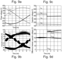
- Fig. 9a - 9b show schematically characteristic waveforms when a short circuit error in a switching cell occurs.
- Fig. 9a shows phase voltages of the grid
- Fig. 9b shows inductor currents
- Fig. 9c shows capacitor voltages
- Fig. 9d shows voltage differences between adjacent capacitors.
- Fig. 9a - 9d show the waveforms for a short-circuit fault in cell 140 of phase A (such as the one shown in Fig. 1 ) of a 3-phase 5-level flying capacitor converter system 100.
- the flying capacitor voltages on either side of the faulted cell will start changing, as show in Fig. 9c .
- This fast change in the voltage can be used for error detection and at the same time to identify the faulty cell, cell 140 in this case.
- the phase current is almost not affected by this fault except for a higher current ripple.
- alternative the voltage across each individual MOSFET could be measured to detect and identify the failed device.
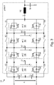
- Fig. 3 schematically shows an example of a flying capacitor converter 100 according to an embodiment.
- first bypass switches 123, 143, 163, 183 and second bypass switches 125, 145, 165, 185 are arranged in parallel to the respective first converter switches 122, 142, 162, 182 and the respective second converter switches 124, 144, 164, 184.
- the converter is provided with bypass switches in parallel to the main switches. These switches may be of any type, semiconductors, relays etc. as shown in Fig. 3 . Additional semiconductors to disconnect the flying capacitors may be inserted, but are not obligatory.
- To bypass one switching cell all semiconductors in this cell need to be bypassed, e.g. if cell 140 has to be bypassed, bypass switches 143 and 145 need to be closed.
- the capacitors need to be discharged (either partially of completely) to provide safe conditions for the reconfiguration of the converter system. Afterwards, all semiconductors of the faulty switching cell are shorted by the bypass switches. Now the system is a (n-1)-level system, since it has reduced from n+1 cells to n cells, thus the modulation has to be adapted too, e.g. in the standard phase-shifted carrier modulation, the carrier for the faulty switching cell has to be removed and the phase shift between the remaining carriers needs to be adjusted. Afterwards, the system can be restarted. This means the flying capacitors need to be charged again. Finally, the power conversion can be continued.
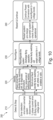
- Fig. 10 shows schematically a fault handling strategy 200.
- a single switch fault can be detected, identified and the system can be reconfigured.
- the whole process can be summarized as follows:
- 210 once the error is detected, the system is stopped and then disconnected from the grid in order to protect the devices from overvoltages and/or over currents.
- 220 it is determined if it is an open-circuit error (222) or a short-circuit error (224).
- a short-circuit error the identification of the faulty switching cell can easily be done by measuring the flying capacitor voltages.
- a diagnostic procedure e.g. executing a sequence of switching vectors as described above, can be applied to identify the faulty switching cell.
- the flying capacitors are either fully discharged or to values at which a safe bypassing of the faulty switching cell by bypass switches is possible. Since now one switching cell is bypassed the converter has (n-1) voltage levels and accordingly the modulation scheme needs to be adapted too. Once this is done, the system can be restarted, in 242. Before continuing the power conversion, in 244, there may be an initial check of the functionalities in the converter system.
- Fig. 11 shows a flow diagram 900 according to an embodiment.
- a faulty converter level is detected, wherein the faulty converter level comprises the first converter switch 122, 142, 162, 182 (see, e.g., Fig. 1 ) and/or the second converter switch 124, 144, 164, 184 being faulty.
- the multi-level converter are disconnected from an input voltage.
- all capacitors arranged in parallel to the input of the multi-level converter are discharged, wherein all capacitors 127, 147, 167 comprise the converter capacitors and an input capacitor 112, 114.
- the first bypass switch and the second bypass switch of the faulty converter level are closed.
- a modulation of the converter switches of the other converter levels is adapted.
- the multi-level converter is restarted.
- an initial check of the multi-level converter is conducted.
- the multi-level converter continues to run.
Landscapes
- Engineering & Computer Science (AREA)
- Power Engineering (AREA)
- Inverter Devices (AREA)
Abstract
detecting a faulty converter level, wherein the faulty converter level comprises the first converter switch (122, 142, 162, 182) and/or the second converter switch (124, 144, 164, 184) being faulty;
discharging all capacitors arranged in parallel to the input of the multi-level converter (100), wherein all capacitors comprise the converter capacitors (127, 147, 167) and an input capacitor (112, 114);
closing the first bypass switch (123, 143, 163, 183) and the second bypass switch (125, 145, 165, 185) of the faulty converter level;
adapting a modulation of the converter switches of the other converter levels; and restarting the multi-level converter (100).
Description
- The invention relates to the field of multi-level flying capacitor converter, particularly for compensating a faulty switch in a multi-level flying capacitor converter. The invention further relates to a method, to a use, to a program element, and to a computer-readable storage medium.
- A converter that uses a flying capacitor multilevel topology may bring many benefits, for instance a significant converter weight reduction. Hence, it is desirable to increase the availability of the multi-level flying capacitor converter.
- It is an objective of the invention to provide a means for an improved availability and/or reliability of a multi-level flying capacitor converter. This objective is achieved by the subject-matter of the independent claims. Further embodiments are evident from the dependent claims and the following description.
- One aspect relates to a method for compensating a faulty switch in a multi-level flying capacitor converter, wherein each converter level of the multi-level converter comprises a converter capacitor, arranged in parallel to an input of the multi-level converter, a first converter switch and a second converter switch, arranged between a first end or a second end of the converter capacitor respectively, and a first bypass switch and a second bypass switch, arranged in parallel to the respective first converter switch and the respective second converter switch. The method comprising the steps of:
- detecting a faulty converter level, wherein the faulty converter level comprises the first converter switch and/or the second converter switch being faulty;
- discharging all capacitors arranged in parallel to the input of the multi-level converter, wherein all capacitors comprise the converter capacitors and an input capacitor;
- closing the first bypass switch and the second bypass switch of the faulty converter level;
- adapting a modulation of the converter switches of the other converter levels; and restarting the multi-level converter.
- The multi-level flying capacitor converter converts an input DC signal into an AC output signal. The AC output signal may have one phase or more phases, for example three phases. Embodiments of the multi-level converter may be designed for low voltages, e.g. 5 V, other embodiments may be designed for low voltages, e.g. in a voltage range of 230 V, 1 kV, and/or other voltage range, and another embodiments be designed for variable voltages. The power transformed by the multi-level converter may range between a few watts, up to a MW range.
- The multi-level flying capacitor converter basically comprises a plurality of "levels", each of these levels comprising a "flying capacitor" or converter capacitor, which is charged by one or two switches upstream and discharged by the one or two switches downstream. The "flying capacitor" or converter capacitor is arranged in parallel to the input of the multi-level converter. Each of the one or two switches - i.e. the first converter switch and, optionally, the second converter switch - is arranged between a first end or a second end of the converter capacitor respectively. The first bypass switch and the (optional, if there is a second converter switch) second bypass switch are arranged in parallel to the respective first converter switch and the respective second converter switch. The converter switch may be implemented by a semiconductor, for instance by a FET, e.g. a MOSFET (metal-oxide-semiconductor field-effect transistor), or an IGBT (insulated gate bi-polar junction transistor). At least in some embodiments, a capacitor may be arranged in parallel to the converter switch, to improve the electrical behaviour. At least in some embodiments, the converter capacitor, which would be directly connected to the one or two switches of the last level, may be lacking. In some embodiments, there may be an output low-pass after the last level, the low-pass comprising an inductor followed by a capacitor.
- A faulty converter level is a level of the multi-level converter, which has a faulty first converter switch and/or a faulty second converter switch. For most multi-level converters, it may be a rare event that both converter switch become faulty at the same time. Detecting a faulty converter level may include to identify the faulty converter switch and/or the kind of fault, i.e. an open-circuit failure or short circuit failure. Once an error - i.e. the faulty converter level - is detected, the system may be stopped and then disconnected from the grid (e.g. AC grid, or another (rectified) DC input voltage) in order to protect the devices from over-voltages and/or over-currents. After detecting a faulty converter level, all capacitors arranged in parallel to the input of the multi-level converter are discharged. The term "all capacitors" may - besides the converter capacitors - also comprise more capacitors, e.g. also one or more input capacitor(s) and/or one or more output capacitor(s). The discharging may, for instance, be performed by closing all the bypass switches, and/or by other means. The discharging may be a complete or a partial discharging, at least to a charging-level where a safe bypassing of the faulty switching cell by bypass switches is possible.
- After the discharging, all switches of the faulty switching cell are shorted by the bypass switches, by closing the first bypass switch and the (optional) second bypass switch of the faulty converter level. Shorting the bypass switches reduces one level of the multilevel converter, i.e. it makes the n-level converter an (n-1)-level converter. After the shorting - done by closing the bypass switch(es) -, the modulation of the converter switches of the other (or "remaining") converter levels has to be adapted. The adapting of the modulation may comprise removing the carrier for the faulty switching cell, and adjusting the phase shift between the remaining carriers, i.e. of the remaining levels. With this adapted modulation, the multi-level converter may be restarted. The restarting may be followed by continuing to run the multi-level converter.
- This method increases the availability of the multi-level flying capacitor converter significantly, because a faulty switch does not immediately lead to a fail of the multilevel converter. Moreover, a multi-level converter, which may be selected for behavioural reasons, may additionally bring the benefit of higher availability and/or reliability. Using the architecture described above and/or below, the multi-level converters may - depending on the number of levels - even tolerate a double failure or even a failure of a higher degree.
- In various embodiments, the method further comprises the step of conducting an initial check of the multi-level converter before continuing to run the multi-level converter. The initial check may comprise to check the functionalities in the converter system, for instance to check - after the capacitors have been charged again -if their voltages are balanced.
- In various embodiments, a detecting of the faulty converter level may be performed, wherein the faulty converter level comprises the first converter switch and/or the second converter switch being faulty. The converter switch may have a short-circuit error or an open-circuit error.
- In various embodiments, the identifying the converter switch having an open-circuit error comprises to measure a maximum voltage at one of the converter capacitors, and/or to apply a sequence of switching vectors to the switches of the multi-level flying capacitor converter. Details are given below.
- In various embodiments, the identifying the converter switch having a short-circuit error comprises to measure a zero difference voltage between two of the converter capacitors. Details are given below.
- An aspect relates to a multi-level flying capacitor converter for DC/AC converting, wherein each converter level of the multi-level converter comprises:
- a converter capacitor, arranged in parallel to an input of the multi-level converter;
- a first converter switch and a second converter switch, arranged between a first end or a second end of the converter capacitor respectively;
- a first bypass switch and a second bypass switch, arranged in parallel to the respective first converter switch and the respective second converter switch; and
- a control unit configured for conducting a method ass described above and/or below.
- In various embodiments, the multi-level converter comprises between 2 and 10 converter levels, particularly between 3 and 6 converter levels. More levels may lead to a smoother behaviour of the multi-level converter. However, additional steps may also increase the costs for the converter. Hence, it turned out that a good compromise may be to use between 3 and 6 converter levels, for
instance - In various embodiments, the multi-level converter further comprises an input capacitor and/or an output low-pass. The output low-pass may comprise an inductor arranged in series to the output and a capacitor arranged in parallel to the output, e.g. after the inductor. This may contribute to less distortion or harmonic distortion of the output signal of the multi-level converter.
- An aspect relates to a computer program product comprising instructions, which, when the program is executed by a control unit, cause the control unit to carry out the method as described above and/or below.
- An aspect relates to a computer-readable storage medium where a computer program or a computer program product as described above is stored on.
- An aspect relates to a use of a multi-level converter described above and/or below or a method described above and/or below for a PV (photovoltaic) inverter, UPS (uninterrupted power supply) systems, high-speed drives or motors, BESS (battery energy storage system), EV (electric vehicle) charging, and/or further DC/AC converting systems.
- For further clarification, the invention is described by means of embodiments shown in the figures. These embodiments are to be considered as examples only, but not as limiting.
- The drawings depict drawings of an embodiment or of a sub-circuit of an embodiment:
- Fig. 1
- schematically an example of a flying capacitor converter;
- Fig. 2a
- schematically an example of an open-circuit failure;
- Fig. 2b
- schematically an example of a short-circuit failure;
- Fig. 3
- schematically an example of a flying capacitor converter;
- Fig. 4a and 4b
- schematically an example of an inverter operation of a 5-level flying capacitor system;
- Fig. 5a and 5b
- schematically an example of another inverter operation of a 5-level flying capacitor system;
- Fig. 6a and 6b
- schematically an example of a rectifier operation of a 5-level flying capacitor system;
- Fig. 7a and 7b
- schematically an example of another rectifier operation of a 5-level flying capacitor system;
- Fig. 8a and 8b
- schematically examples of test vectors to identify a faulty switching cell;
- Fig. 9a - 9d
- schematically characteristic waveforms when a short circuit error in a switching cell occurs;
- Fig. 10
- schematically a fault handling strategy;
- Fig. 11
- a flow diagram.
-
Fig. 1 shows schematically an example of a flyingcapacitor converter 100, particularly a 5-level flying capacitor converter comprising 4 flying capacitor cells. The converter shown depicts MOSFETs (metal-oxide-semiconductor field-effect transistors) asswitches capacitor converter system 100, there are two failure cases considered: An open-circuit failure, where the switch does not turn-on anymore, and a short-circuit failure, where the switch cannot be turned-off anymore. The detection of these two error cases based on the flying capacitor voltage and the inductor current measurement for different operating modes (inverter or rectifier) are described in detail below. Furthermore, a possible reconfiguration process is described in detail, which advantageously allows to reconfigure the system in a safe way without risking additional destruction of the system. -
Fig. 2a shows schematically an example of an open-circuit failure in anexample cell 140. Aconverter switch 142 and/or 144 may fail by itself, and/or it may be possible that a gate drive circuit of the switch has failed. Either case may lead to a possible situation that the switch has failed in open circuit and cannot be turned-on again. In this scenario, a direction of a sinusoidal phase current iL (see, e.g.,Fig. 1 ) is considered positive (iL > 0) and towards the grid. In the negative half-cycle (iL < 0), this direction reverses and the phase current is flowing towards the converter. - In the inverter mode (see, e.g., converter of
Fig. 1 , or waveforms as shownFig. 4a and Fig. 4b ) iL is assumed being is in its positive half-cycle (iL > 0), so flowing towards the grid. In a case whenswitch 142 fails in open, then in the next few switching cycles, the flyingcapacitor 127 can only be charged, while 147 can only be discharged, since the charging current would be blocked by the open-circuitedswitch 142. Accordingly, the voltage difference between Vcf1 and Vcf2 is increasing rapidly. The other capacitor voltages may also adapt, but much slower than the two flying capacitors on either side of the failed switch. Ifswitch 142 fails while the current iL is in the negative half cycle (iL < 0), flowing towards the converter, then the converter operation is not affected, since the diode of theswitch 142 takes over the operation. Under such a condition, an open circuit failure of theswitch 142 cannot be detected immediately. One would have to wait until the positive half-cycle arrives. - If the open-circuit failure happens during the positive half-cycle of the phase-current, the current reduces to zero, and if the open circuit fault happens just before the positive half-cycle arrives, then the current would hover around zero in the positive half-cycle. This happens, because the applied voltage on the phase by the converter will be on an average negative and thus lower than expected. To understand the behaviour in terms of the switching vectors that are applied when the current is in positive direction, due to the un-operational switch, more zero and/or negative vectors get applied to the output - e.g. a sequential "1110" would become "1010" -, the midpoint to converter output voltage (i.e. voltage measured between node 'A' and node 'N', wherein node 'N' is a mid-point node) Vmid-out =+1/4 Vdc would become zero, i.e. Vmid-out=0. If a closed loop current control is presented, the controller will counteract this distortion, resulting in a high voltage imbalance on the flying capacitor voltages.
- In rectifier mode and assuming iL is in the negative-half c cycle (iL < 0), the converter would still behave normally (like a boost converter), even if
switch 142 suffers an open-circuit failure since the diode ofswitch 142 is still operating, and thus the open circuit failure ofswitch 142 cannot be detected. If iL is in the positive-half cycle (iL > 0), the converter behaves like a regular-diode rectifier, sinceswitch 142 is not operating and thus behaves like a diode only and switch 144 when turned-on, would only take the current of its diode that is flowing in the same direction. This results in a pure diode rectifier type of phase that will have significant distortion. -
Fig. 2b shows schematically an example of a short-circuit failure in anexample cell 140. A switch can fail by itself, and/or it may be possible that a gate drive circuit of the switch has failed. Either case may lead to a possible situation that the switch has failed in short circuit. In this scenario, the direction of the sinusoidal phase current iL is considered positive (iL > 0), and towards the grid if its flowing in the direction as shown inFig. 1 . In the negative half-cycle (iL < 0), this direction reverses and the phase current is flowing towards the converter. - If,
e.g. switch 142 fails in short-circuit, and switch 144 is turned on, a high current will flow through the two switches switch 142 and switch 144, chargingcapacitor 147 and dischargingcapacitor 127, as shown inFig. 2b . Accordingly, Vcf1 will fall and Vcf2 will rise until both capacitors have the same voltage. This error is independent of the direction of iL. Assuming that the semiconductors are not destroyed during the recharging process of the two now short-circuited flying capacitors, the short-circuit fault has no big impact on the output current. In the considered case, the system changes from a five to a four-level system and therefore higher distortions in the output current will be observed due to the increased switched voltage or reduced voltage-levels at the converter's output. However, this may not be the case and the overcurrent in the switches at the instant of fault could cause overheating to such an extent that switch will be destroyed and the system can no longer operate normally. In short-circuit failure, the cases of inverter and rectifier operation may not needed to be separated. - As discussed above, there are two error cases considered for a flying capacitor converter: a device failing in open circuit or in short circuit. For the following, an n-level flying capacitor converter system is considered, with the
capacitor 127 at the highest voltage Vcf1, and Cf(n-2) with the lowest flying capacitor voltage, Vcf(n-2). To keep the annotation simple, the DC-link capacitors - The system has (n-1) switching cells, whereas - for example - switching
cell 140 is located betweencapacitors capacitors -
Fig. 4a and 4b show schematically an example of an inverter operation of a 5-level flyingcapacitor system 100.Fig. 4a shows inductor currents andFig. 4b shows capacitor voltages when an open-circuit error in thehigh side device 142 of switchingcell 140 in phase a occurs during the positive half-cycle of i(L,a).Fig. 5a and 5b show schematically an example of another inverter operation of a 5-level flyingcapacitor system 100.Fig. 5a shows inductor currents, andFig. 5b shows capacitor voltages when an open-circuit error in the high side device of switchingcell 140 in phase a occurs during the negative half-cycle of i(L,a). The area of about 5.5 ms indicates the time range when the error could have happened. - To detect if a device has failed in an open-circuit and cannot be turned on again, the phase current can be used.
Fig. 4a, 4b ,5a and 5b depict the situation when the high side device switch 142 (see, e.g.,Fig. 1 ) in switchingcell 140 of the phase, say phase A of a 3-phase inverter/rectifier, is failing. As seen in all figures, the phase current can be used to detect an open circuit fault in the switch, for example by comparing it to a reference band as illustrated with dashed lines. Alternatively, other measurements can be used to detect an error. However, at the time instant of the fault detection the deviation of the capacitor voltages may be too slow to allow a speedy identification of the switch failure. In the considered example this is especially the case if the open-circuit with highside device switch 142 fault happens during the negative half-cycle of the current (seeFigs. 4a - 5b ). Therefore, information from the current sensor may be used to instead. -
Fig. 6a and 6b show schematically an example of a rectifier operation of a 5-level flying capacitor system.Fig. 6a shows inductor currents, andFig. 6b shows capacitor voltages when an open-circuit error in the high side device of switchingcell 140 in phase A occurs during the positive half-cycle of i(L,a).Fig. 7a and 7b show schematically an example of another rectifier operation of a 5-level flying capacitor system.Fig. 7a shows inductor currents, andFig. 7b shows capacitor voltages when an open-circuit error in the high side device of switchingcell 140 in phase a occurs during the negative half-cycle of i(L,a). The area of about 5.5 ms indicates the time range when the error could have happened. -
Fig. 8a and 8b show schematically examples of test vectors to identify a faulty switching cell.Fig. 8a shows a sequence of switching vectors, andFig. 8b shows two switching vectors. - The faulty switching cell may be identified by measuring the deviation in flying capacitor voltages:

Fig. 5a, 5b andFig. 7a,7b , the deviation on the flying capacitor voltage may, in some cases, not be significant enough. Thus, after turning off the converter system and disconnect it from the grid, or another power source rectified to DC, a diagnostic procedure might be necessary in order to identify the faulty switching cell. In this procedure, for the purpose of cell identification a sequence of switching vectors can be applied on the faulty phase or all phases after disconnecting the system from the grid. Two examples of such switching vector sequences are shown next to further explain the idea. - Example 1: In
Fig. 8a at t0, after an open circuit fault inswitch 162 has occurred. This fault is detected, and the converter is turned off and disconnected from the grid. To identify where exactly the fault has developed, a sequence of switching vectors is applied by cycling the phase voltage from a maximum possible negative voltage level to the maximum possible positive voltage level. The faulty switching cell can be found by either measuring the flying capacitor voltage or the converter output voltage. For example, at t3, switch 162 should be switched on but it stays open due to the fault. Thus, no change in the difference of flying capacitor voltages Vcf nor any change in the phase voltage is seen and thus, the failed device is identified. - Example 2: In
Fig. 8b at t0, after an open circuit fault inswitch 162 has occurred. This fault is detected, and the converter is turned off and disconnected from the grid. To identify where exactly the fault has developed, a sequence of switching vectors is applied, first all low side devices are turned on at t1, afterwards at t2 all high side devices are turned on. Sinceswitch 162 cannot be turned on again, the voltage difference ΔV in the flying capacitor voltages Vcf2 (charged) and Vcf3 (discharged) can be observed and accordingly the faulty switching cell can be identified. If the direction of current was known when the fault was detected, then even the faulty device within that cell can be identified, say for the purpose of service and maintenance. - There may be further alternative sequences of switching vectors that can be applied, whereas the faulty cell or device can be found by measuring the flying capacitor voltages, converter output voltage or the phase current. To ensure a proper identification of the faulty switching cell, this procedure might be applied to all the phases, to remove any phase ambiguity.
- Additionally or as an alternative, the voltages across all individual switches (e.g. the positive or negative terminals of adjacent flying capacitors) may be measured. These measured voltages may be compared to the current switching state such that an open circuit (or short circuit) can be immediately detected by comparing it to the current switching state. However, for each switch one voltage measurement is required. Thus, for a n-
level system 2·(n-1) voltage measurements, instead of (n-2) voltage measurements, for the flying capacitors are required. - In case of a short-circuit failure in cell i, the voltage vcf(i-1) will immediately fall and vcfi will raise until they are equal. Assuming the devices are not destroyed, the phase current will not be affected, except for higher distortions due to imbalanced flying capacitor voltages and missing voltage level. In a short-circuit fault, first the imbalance of the flying capacitor voltages is detected, and an error signal is generated. Across the faulty cell the voltage difference between the neighbouring flying capacitors, Δvcfi, will be quickly reduced to almost zero. This allows to determine the faulty phase and identify the affected switching cell:

-
Fig. 9a - 9b show schematically characteristic waveforms when a short circuit error in a switching cell occurs.Fig. 9a shows phase voltages of the grid,Fig. 9b shows inductor currents,Fig. 9c shows capacitor voltages, andFig. 9d shows voltage differences between adjacent capacitors. -
Fig. 9a - 9d show the waveforms for a short-circuit fault incell 140 of phase A (such as the one shown inFig. 1 ) of a 3-phase 5-level flyingcapacitor converter system 100. Immediately after the fault happens the flying capacitor voltages on either side of the faulted cell will start changing, as show inFig. 9c . Although it is possible to detect the short-circuit with the measured absolute voltage of the flying capacitors, again the difference of voltage between the adjacent flying capacitors may be used, as shown inFig. 9d . It clearly shows a possible problem withcell 140, since here ΔVcf2=vcf1-vcf2 has reduced to almost zero. This fast change in the voltage can be used for error detection and at the same time to identify the faulty cell,cell 140 in this case. The phase current is almost not affected by this fault except for a higher current ripple. As mentioned above in the open circuit detection, alternative the voltage across each individual MOSFET could be measured to detect and identify the failed device. -
Fig. 3 schematically shows an example of a flyingcapacitor converter 100 according to an embodiment. Compared toFig. 1 , first bypass switches 123, 143, 163, 183 and second bypass switches 125, 145, 165, 185 are arranged in parallel to the respective first converter switches 122, 142, 162, 182 and the respective second converter switches 124, 144, 164, 184. Using this architecture, once the faulty switching cell is identified, the converter may be reconfigured to work with one cell less. The converter is provided with bypass switches in parallel to the main switches. These switches may be of any type, semiconductors, relays etc. as shown inFig. 3 . Additional semiconductors to disconnect the flying capacitors may be inserted, but are not obligatory. To bypass one switching cell, all semiconductors in this cell need to be bypassed, e.g. ifcell 140 has to be bypassed, bypass switches 143 and 145 need to be closed. - First, the capacitors need to be discharged (either partially of completely) to provide safe conditions for the reconfiguration of the converter system. Afterwards, all semiconductors of the faulty switching cell are shorted by the bypass switches. Now the system is a (n-1)-level system, since it has reduced from n+1 cells to n cells, thus the modulation has to be adapted too, e.g. in the standard phase-shifted carrier modulation, the carrier for the faulty switching cell has to be removed and the phase shift between the remaining carriers needs to be adjusted. Afterwards, the system can be restarted. This means the flying capacitors need to be charged again. Finally, the power conversion can be continued.
-
Fig. 10 shows schematically afault handling strategy 200. With the methods described above a single switch fault can be detected, identified and the system can be reconfigured. The whole process can be summarized as follows: In 210, once the error is detected, the system is stopped and then disconnected from the grid in order to protect the devices from overvoltages and/or over currents. In 220, it is determined if it is an open-circuit error (222) or a short-circuit error (224). In case of a short-circuit error, the identification of the faulty switching cell can easily be done by measuring the flying capacitor voltages. In case of an open-circuit error a diagnostic procedure, e.g. executing a sequence of switching vectors as described above, can be applied to identify the faulty switching cell. In 230, the flying capacitors are either fully discharged or to values at which a safe bypassing of the faulty switching cell by bypass switches is possible. Since now one switching cell is bypassed the converter has (n-1) voltage levels and accordingly the modulation scheme needs to be adapted too. Once this is done, the system can be restarted, in 242. Before continuing the power conversion, in 244, there may be an initial check of the functionalities in the converter system. -
Fig. 11 shows a flow diagram 900 according to an embodiment. In a step 902 a faulty converter level is detected, wherein the faulty converter level comprises thefirst converter switch Fig. 1 ) and/or thesecond converter switch optional step 904, the multi-level converter are disconnected from an input voltage. In astep 906 all capacitors arranged in parallel to the input of the multi-level converter are discharged, wherein allcapacitors input capacitor step 908, the first bypass switch and the second bypass switch of the faulty converter level are closed. In astep 910, a modulation of the converter switches of the other converter levels is adapted. In astep 912, the multi-level converter is restarted. In anoptional step 914, an initial check of the multi-level converter is conducted. In anoptional step 916, the multi-level converter continues to run.
Claims (14)
- A method for compensating a faulty switch (122, 124, 142, 144, 162, 164, 182, 184) in a multi-level flying capacitor converter (100), wherein each converter level of the multi-level converter (100) comprisesa converter capacitor (127, 147, 167), arranged in parallel to an input of the multi-level converter (100),a first converter switch (122, 142, 162, 182) and a second converter switch (124, 144, 164, 184), arranged between a first end or a second end of the converter capacitor (127, 147, 167) respectively, anda first bypass switch (123, 143, 163, 183) and a second bypass switch (125, 145, 165, 185), arranged in parallel to the respective first converter switch (122, 142, 162, 182) and the respective second converter switch (124, 144, 164, 184),the method comprising the steps of:detecting a faulty converter level, wherein the faulty converter level comprises the first converter switch (122, 142, 162, 182) and/or the second converter switch (124, 144, 164, 184) being faulty;discharging all capacitors arranged in parallel to the input of the multi-level converter (100), wherein all capacitors comprise the converter capacitors (127, 147, 167) and an input capacitor (112, 114);closing the first bypass switch (123, 143, 163, 183) and the second bypass switch (125, 145, 165, 185) of the faulty converter level;adapting a modulation of the converter switches of the other converter levels; andrestarting the multi-level converter (100).
- The method of claim 1, further comprising the step of:
continuing to run the multi-level converter (100). - The method of claim 1 or 2, further comprising the step of:
before discharging all capacitors, disconnecting the multi-level converter (100) from an input voltage (VDC). - The method of any one of the preceding claims, further comprising the step of:
before continuing to run the multi-level converter (100), conducting an initial check of the multi-level converter (100). - The method of any one of the preceding claims,
wherein discharging all capacitors comprises to discharge the capacitors either partially of completely. - The method of any one of the preceding claims,
wherein detecting a faulty converter level comprises identifying the first converter switch (122, 142, 162, 182) and/or the second converter switch (124, 144, 164, 184) having a short-circuit error or an open-circuit error. - The method of claim 6,wherein identifying the converter switch having an open-circuit error comprises to measure a maximum voltage at one of the converter capacitors (127, 147, 167), and/orto apply a sequence of switching vectors to the switches (122, 124, 142, 144, 162, 164, 182, 184) of the multi-level flying capacitor converter (100).
- The method of claim 6,
wherein identifying the converter switch having a short-circuit error comprises to measure a zero difference voltage between two of the converter capacitors (127, 147, 167). - A multi-level flying capacitor converter for DC/AC converting, wherein each converter level of the multi-level converter (100) comprises:a converter capacitor (127, 147, 167), arranged in parallel to an input of the multi-level converter (100);a first converter switch (122, 142, 162, 182) and a second converter switch (124, 144, 164, 184), arranged between a first end or a second end of the converter capacitor (127, 147, 167) respectively;a first bypass switch (123, 143, 163, 183) and a second bypass switch (125, 145, 165, 185), arranged in parallel to the respective first converter switch (122, 142, 162, 182) and the respective second converter switch (124, 144, 164, 184); anda control unit configured for conducting a method according to any one of the preceding claims.
- The multi-level converter (100) of claim 9,
wherein the multi-level converter (100) comprises between 2 and 10 converter levels, particularly between 3 and 6 converter levels. - The multi-level converter (100) of claim 9 or 10, further comprising:an input capacitor (102, 104); and/oran output low-pass (192, 194).
- A computer program product comprising instructions, which, when the program is executed by a control unit, cause the control unit to carry out the method according to any one of the claims 1 to 8.
- A computer-readable storage medium where a computer program according to claim 12 is stored on.
- Use of a multi-level converter (100) according to any one of claims 9 to 11 or a method according to any one of claims 1 to 8 for a PV (photovoltaic) inverter, UPS (uninterrupted power supply) systems, high-speed drives or motors, BESS (battery energy storage system), EV (electric vehicle) charging, and/or further DC/AC converting systems.
Priority Applications (3)
| Application Number | Priority Date | Filing Date | Title |
|---|---|---|---|
| EP21196669.2A EP4148964A1 (en) | 2021-09-14 | 2021-09-14 | A method and a device for compensating a faulty switch in a multi-level flying capacitor converter |
| US17/943,693 US20230083355A1 (en) | 2021-09-14 | 2022-09-13 | Method and a Device for Compensating a Faulty Switch in a Multi-Level Flying Capacitor Converter |
| CN202211110625.4A CN115811212A (en) | 2021-09-14 | 2022-09-13 | Method and apparatus for compensation of a faulty switch in a multilevel flying capacitor converter |
Applications Claiming Priority (1)
| Application Number | Priority Date | Filing Date | Title |
|---|---|---|---|
| EP21196669.2A EP4148964A1 (en) | 2021-09-14 | 2021-09-14 | A method and a device for compensating a faulty switch in a multi-level flying capacitor converter |
Publications (1)
| Publication Number | Publication Date |
|---|---|
| EP4148964A1 true EP4148964A1 (en) | 2023-03-15 |
Family
ID=77774707
Family Applications (1)
| Application Number | Title | Priority Date | Filing Date |
|---|---|---|---|
| EP21196669.2A Pending EP4148964A1 (en) | 2021-09-14 | 2021-09-14 | A method and a device for compensating a faulty switch in a multi-level flying capacitor converter |
Country Status (3)
| Country | Link |
|---|---|
| US (1) | US20230083355A1 (en) |
| EP (1) | EP4148964A1 (en) |
| CN (1) | CN115811212A (en) |
Families Citing this family (4)
| Publication number | Priority date | Publication date | Assignee | Title |
|---|---|---|---|---|
| US12040702B2 (en) * | 2021-06-24 | 2024-07-16 | Murata Manufacturing Co., Ltd. | Multi-level structures and methods for switched-mode power supplies |
| US11936291B2 (en) * | 2021-11-08 | 2024-03-19 | Psemi Corporation | Controlling charge-balance and transients in a multi-level power converter |
| CN117233650B (en) * | 2023-11-15 | 2024-03-08 | 希荻微电子集团股份有限公司 | Short circuit detection method and charging system |
| CN117526737B (en) * | 2023-11-20 | 2024-06-07 | 深圳市卓飞电子科技有限公司 | Input rectifying circuit of power supply |
-
2021
- 2021-09-14 EP EP21196669.2A patent/EP4148964A1/en active Pending
-
2022
- 2022-09-13 US US17/943,693 patent/US20230083355A1/en active Pending
- 2022-09-13 CN CN202211110625.4A patent/CN115811212A/en active Pending
Non-Patent Citations (4)
| Title |
|---|
| AMINI JALAL ET AL: "A Fault-Diagnosis and Fault-Tolerant Control Scheme for Flying Capacitor Multilevel Inverters", IEEE TRANSACTIONS ON INDUSTRIAL ELECTRONICS, IEEE SERVICE CENTER, PISCATAWAY, NJ, USA, vol. 64, no. 3, 1 March 2017 (2017-03-01), pages 1818 - 1826, XP011640767, ISSN: 0278-0046, [retrieved on 20170209], DOI: 10.1109/TIE.2016.2624722 * |
| CORZINE K A ET AL: "A Unique Fault-Tolerant Design for Flying Capacitor Multilevel Inverter", IEEE TRANSACTIONS ON POWER ELECTRONICS, INSTITUTE OF ELECTRICAL AND ELECTRONICS ENGINEERS, USA, vol. 19, no. 4, 1 July 2004 (2004-07-01), pages 979 - 987, XP011114978, ISSN: 0885-8993, DOI: 10.1109/TPEL.2004.826495 * |
| KHAN F H ET AL: "A Multilevel Modular Capacitor-Clamped DC-DC Converter", IEEE TRANSACTIONS ON INDUSTRY APPLICATIONS, IEEE SERVICE CENTER, PISCATAWAY, NJ, US, vol. 43, no. 6, 1 November 2007 (2007-11-01), pages 1628 - 1638, XP011197482, ISSN: 0093-9994, DOI: 10.1109/TIA.2007.908176 * |
| LEI HU ET AL: "Reconfiguration of carrier-based modulation strategy for fault tolerant multilevel inverters", INDUSTRIAL ELECTRONICS SOCIETY, 2005. IECON 2005. 31ST ANNUAL CONFERENCE OF IEEE, IEEE, PISCATAWAY, NJ, USA, 6 November 2005 (2005-11-06), pages 1048 - 1053, XP010876080, ISBN: 978-0-7803-9252-6, DOI: 10.1109/IECON.2005.1569049 * |
Also Published As
| Publication number | Publication date |
|---|---|
| US20230083355A1 (en) | 2023-03-16 |
| CN115811212A (en) | 2023-03-17 |
Similar Documents
| Publication | Publication Date | Title |
|---|---|---|
| EP4148964A1 (en) | A method and a device for compensating a faulty switch in a multi-level flying capacitor converter | |
| CN108370221B (en) | Power conversion device | |
| JP6417043B2 (en) | Power converter | |
| EP2383878B1 (en) | System and method for protection of a multilevel converter | |
| EP3422548B1 (en) | Converter device | |
| US20110012543A1 (en) | Electric power converter | |
| US10734916B2 (en) | Power conversion device | |
| US20210384816A1 (en) | Modular multilevel converter system and voltage detection method and open-circuit fault diagnosis method thereof | |
| CA2771910C (en) | Converter cell module, voltage source converter system comprising such a module and a method for controlling such a system | |
| KR20120072362A (en) | Converter with active fault current limitation | |
| EP2147490A2 (en) | Dynamic voltage sag correction | |
| US10270328B2 (en) | Multilevel converter with energy storage | |
| US20140268942A1 (en) | Interface arrangement between ac and dc systems for reliable opening of the circuit breaker in time | |
| US9780681B2 (en) | Power conversion system including plurality of power converters connected in parallel to load | |
| EP3609069B1 (en) | Converter system | |
| KR20140118394A (en) | multi-level inverter | |
| Lee et al. | A fault detection method in cascaded H-bridge multilevel inverter | |
| Ku et al. | Multiple open-switch faults detection and fautls tolerant method of three-level three-phase NPC active rectifier | |
| US20230327453A1 (en) | Photovoltaic System, Protection Method, and Inverter System | |
| Halabi et al. | Fault diagnosis and tolerance for open-circuit faults in multi-level inverters | |
| Abuelnaga et al. | Open circuit IGBT fault classification using phase current in a CHB converter | |
| Azimipanah et al. | Open circuit fault detection and diagnosis for seven-level hybrid active neutral point clamped (ANPC) multilevel inverter | |
| US20210044142A1 (en) | Uninterrupted power supply apparatus | |
| Pallo et al. | Short-circuit fault ride-through of flying-capacitor multilevel converters through rapid fault detection and idle-mode operation | |
| CN110308341B (en) | Inversion module detection method, device and system in energy conversion system |
Legal Events
| Date | Code | Title | Description |
|---|---|---|---|
| PUAI | Public reference made under article 153(3) epc to a published international application that has entered the european phase |
Free format text: ORIGINAL CODE: 0009012 |
|
| STAA | Information on the status of an ep patent application or granted ep patent |
Free format text: STATUS: THE APPLICATION HAS BEEN PUBLISHED |
|
| AK | Designated contracting states |
Kind code of ref document: A1 Designated state(s): AL AT BE BG CH CY CZ DE DK EE ES FI FR GB GR HR HU IE IS IT LI LT LU LV MC MK MT NL NO PL PT RO RS SE SI SK SM TR |
|
| STAA | Information on the status of an ep patent application or granted ep patent |
Free format text: STATUS: REQUEST FOR EXAMINATION WAS MADE |
|
| 17P | Request for examination filed |
Effective date: 20230908 |
|
| RBV | Designated contracting states (corrected) |
Designated state(s): AL AT BE BG CH CY CZ DE DK EE ES FI FR GB GR HR HU IE IS IT LI LT LU LV MC MK MT NL NO PL PT RO RS SE SI SK SM TR |
|
| STAA | Information on the status of an ep patent application or granted ep patent |
Free format text: STATUS: EXAMINATION IS IN PROGRESS |
|
| 17Q | First examination report despatched |
Effective date: 20240213 |