WO2015020185A1 - 固体電解コンデンサ素子 - Google Patents
固体電解コンデンサ素子 Download PDFInfo
- Publication number
- WO2015020185A1 WO2015020185A1 PCT/JP2014/070978 JP2014070978W WO2015020185A1 WO 2015020185 A1 WO2015020185 A1 WO 2015020185A1 JP 2014070978 W JP2014070978 W JP 2014070978W WO 2015020185 A1 WO2015020185 A1 WO 2015020185A1
- Authority
- WO
- WIPO (PCT)
- Prior art keywords
- layer
- electrolytic capacitor
- solid electrolytic
- capacitor element
- insulator layer
- Prior art date
- Legal status (The legal status is an assumption and is not a legal conclusion. Google has not performed a legal analysis and makes no representation as to the accuracy of the status listed.)
- Ceased
Links
Classifications
-
- H—ELECTRICITY
- H01—ELECTRIC ELEMENTS
- H01G—CAPACITORS; CAPACITORS, RECTIFIERS, DETECTORS, SWITCHING DEVICES, LIGHT-SENSITIVE OR TEMPERATURE-SENSITIVE DEVICES OF THE ELECTROLYTIC TYPE
- H01G9/00—Electrolytic capacitors, rectifiers, detectors, switching devices, light-sensitive or temperature-sensitive devices; Processes of their manufacture
- H01G9/004—Details
- H01G9/04—Electrodes or formation of dielectric layers thereon
- H01G9/042—Electrodes or formation of dielectric layers thereon characterised by the material
-
- H—ELECTRICITY
- H01—ELECTRIC ELEMENTS
- H01G—CAPACITORS; CAPACITORS, RECTIFIERS, DETECTORS, SWITCHING DEVICES, LIGHT-SENSITIVE OR TEMPERATURE-SENSITIVE DEVICES OF THE ELECTROLYTIC TYPE
- H01G9/00—Electrolytic capacitors, rectifiers, detectors, switching devices, light-sensitive or temperature-sensitive devices; Processes of their manufacture
- H01G9/0029—Processes of manufacture
- H01G9/0032—Processes of manufacture formation of the dielectric layer
-
- H—ELECTRICITY
- H01—ELECTRIC ELEMENTS
- H01G—CAPACITORS; CAPACITORS, RECTIFIERS, DETECTORS, SWITCHING DEVICES, LIGHT-SENSITIVE OR TEMPERATURE-SENSITIVE DEVICES OF THE ELECTROLYTIC TYPE
- H01G9/00—Electrolytic capacitors, rectifiers, detectors, switching devices, light-sensitive or temperature-sensitive devices; Processes of their manufacture
- H01G9/004—Details
- H01G9/04—Electrodes or formation of dielectric layers thereon
- H01G9/042—Electrodes or formation of dielectric layers thereon characterised by the material
- H01G9/0425—Electrodes or formation of dielectric layers thereon characterised by the material specially adapted for cathode
-
- H—ELECTRICITY
- H01—ELECTRIC ELEMENTS
- H01G—CAPACITORS; CAPACITORS, RECTIFIERS, DETECTORS, SWITCHING DEVICES, LIGHT-SENSITIVE OR TEMPERATURE-SENSITIVE DEVICES OF THE ELECTROLYTIC TYPE
- H01G9/00—Electrolytic capacitors, rectifiers, detectors, switching devices, light-sensitive or temperature-sensitive devices; Processes of their manufacture
- H01G9/004—Details
- H01G9/07—Dielectric layers
-
- H—ELECTRICITY
- H01—ELECTRIC ELEMENTS
- H01G—CAPACITORS; CAPACITORS, RECTIFIERS, DETECTORS, SWITCHING DEVICES, LIGHT-SENSITIVE OR TEMPERATURE-SENSITIVE DEVICES OF THE ELECTROLYTIC TYPE
- H01G9/00—Electrolytic capacitors, rectifiers, detectors, switching devices, light-sensitive or temperature-sensitive devices; Processes of their manufacture
- H01G9/15—Solid electrolytic capacitors
Definitions
- the present invention relates to a solid electrolytic capacitor element. More specifically, the present invention relates to a solid electrolytic capacitor element whose capacity does not change greatly even when left for a long period of time.
- the solid electrolytic capacitor element is usually formed by laminating an anode body, a dielectric layer, and a cathode layer in this order.
- the cathode layer is usually formed by laminating a semiconductor layer, a carbon layer, and a silver layer in this order from the dielectric layer side.
- the capacitance set to a predetermined value may change.
- the capacity increases in a solid electrolytic capacitor element using an anode body made of tungsten.
- the capacity decreases. Even if the large capacity change is an increase or a decrease, it is not preferable as an electronic component.
- the phenomenon of increased capacity is remarkable in a solid electrolytic capacitor element using an anode body made of tungsten.
- Patent Document 1 discloses an anode body, a dielectric provided on the surface of the anode body, a conductive polymer provided on the surface of the dielectric, and an island shape on the surface of the conductive polymer.
- a solid electrolytic capacitor comprising at least one is disclosed.
- Patent Document 2 discloses a solid electrolytic capacitor in which a dielectric layer, a solid electrolyte layer, a cathode lead layer, and an outer shell resin layer are sequentially formed on the outer side of the anode member, and between the cathode lead layer and the outer shell resin layer, A solid electrolytic capacitor is disclosed in which a protective layer made of a material mainly composed of an inorganic oxide is formed.
- An object of the present invention is to provide a solid electrolytic capacitor element whose capacity does not change greatly even when left for a long period of time.
- a solid electrolytic capacitor element that is 2/3 or more on the basis of
- the insulator layer is made of an inorganic oxide.
- the inorganic oxide includes at least one selected from the group consisting of silicon dioxide, titanium dioxide, zirconium oxide, and hafnium oxide.
- the capacity of the solid electrolytic capacitor element according to the present invention does not change greatly even when left for a long period of time.
- the solid electrolytic capacitor element according to the present invention includes an anode body, a dielectric layer provided so as to cover the anode body, a semiconductor layer provided on the dielectric layer, and an insulation provided on the semiconductor layer.
- the anode body constituting the present invention is not particularly limited as long as it functions as an anode in the solid electrolytic capacitor element.
- the anode body is preferably made of a valve metal or a conductive oxide of the valve metal.
- the valve metal include aluminum, tantalum, niobium, titanium, and tungsten.
- An alloy containing other elements may be used as long as the properties as the anode body are not reduced. Of these, tungsten is preferable because the effects of the present invention are remarkable.
- the granulated powder can be produced by firing and pulverizing the raw metal powder.
- the 50% particle size in the volume-based cumulative particle size distribution of the granulated powder is preferably 20 to 170 ⁇ m, more preferably 26 to 140 ⁇ m.
- the granulated powder is preferably a porous powder formed by sintering raw material metal powder.
- the 50% particle diameter can be calculated by measuring a volume-based particle size distribution by a laser diffraction scattering method using HRA 9320-X100 manufactured by Microtrack Co., Ltd.
- an acid such as sulfuric acid, boric acid, oxalic acid, adipic acid, phosphoric acid or nitric acid; or a solution containing an electrolyte such as an alkali metal salt or ammonium salt of these acids is used.
- the chemical conversion liquid may contain an oxidizing agent that supplies oxygen such as hydrogen peroxide and ozone as long as the effects of the present invention are not impaired.
- a compound that serves as an electrolyte and an oxidizing agent, such as a persulfate can also be used.
- An anode body (hereinafter referred to as a member) that has been subjected to chemical conversion treatment is pulled up from the chemical conversion liquid, washed with pure water, and then dried. Drying can be performed without particular limitation as long as the temperature and time allow the water adhering to the member to evaporate. You may heat-process in order to dry.
- the heat treatment is preferably performed at 250 ° C. or lower, more preferably 160 ° C. to 230 ° C. After this heat treatment, the chemical conversion treatment may be performed again.
- the re-chemical conversion treatment can be performed under the same conditions as the first chemical conversion treatment. After the re-chemical conversion treatment, pure water washing and drying can be performed as described above.
- the semiconductor layer is provided on the dielectric layer obtained by the above method.
- a semiconductor layer will not be specifically limited if it functions as a cathode of a solid electrolytic capacitor element.
- Suitable materials for forming the semiconductor layer include conductive polymers such as polythiophene and derivatives thereof.
- the semiconductor layer made of a conductive polymer can be obtained, for example, by subjecting a precursor (monomer) of a conductive polymer to chemical oxidative polymerization or electrolytic oxidative polymerization on the surface of the dielectric layer.
- the insulator layer is provided on the semiconductor layer.
- the ratio of the portion of the insulator layer having a thickness of 10 nm to 100 nm is 2/3 or more, preferably 3/4 or more, and most preferably 1/1, based on the whole insulator layer.
- the thickness distribution of the insulator layer is determined by observing the fracture surface of the solid electrolytic capacitor element with a scanning electron microscope (SEM), and the thickness of the insulator layer at a location randomly extracted from the SEM observation image. It can be obtained by measuring or analyzing the SEM observation image by a known image processing method.
- the insulator layer preferably has water repellency.
- the insulator layer does not increase the electrical resistance between the semiconductor layer and the carbon layer described later. Specifically, it is preferable to adjust the structure and thickness of the insulator layer on the nano order so that electron transmission occurs due to the tunnel effect or the like.
- the insulator layer is preferably a layer made of nanoparticles, and more preferably a laminate of a plurality of thin layers made of nanoparticles.
- the average particle diameter of the nanoparticles is preferably 1 nm to 90 nm, more preferably 2 nm to 50 nm, and still more preferably 3 nm to 30 nm.
- the average particle diameter of the nanoparticles can be determined by X-ray small angle scattering or the like.
- Preferred nanoparticles constituting the insulator layer include nanoparticles composed of organosilicon compounds such as silicone nanoparticles; nanoparticles composed of inorganic oxides such as silicon dioxide, titanium dioxide, zirconium oxide and hafnium oxide. Of these, silicone nanoparticles and titanium dioxide nanoparticles are preferred. Examples of the titanium dioxide nanoparticles used include those that have been surface-treated with silica, those to which stearic acid has been bonded, and those to which ammonium polyacrylate has been added.
- the insulator layer is not particularly limited by the formation method.
- the insulator layer may be a dispersion of insulator particles (for example, an aqueous dispersion of silicone nanoparticles or titanium dioxide nanoparticles, or a silicone nanoparticle or titanium dioxide nanoparticle) whose concentration is adjusted with a water-soluble organic solvent such as water or alcohol.
- a coating solution composed of particles (sol or the like) can be obtained by coating on a semiconductor layer and then drying.
- a commercial product may be used as the coating solution.
- a liquid solution of silicone nanoparticles for example, trade name “Hajix” manufactured by Comens Co., Ltd., a liquid solution of titanium dioxide nanoparticles manufactured by Ishihara Sangyo Co., Ltd.
- the liquid agent of the titanium dioxide nanoparticles manufactured (for example, coating agent TKC-304 (model number) etc.) can be mentioned.
- the insulator layer manufactured by these methods has water repellency.
- the thickness and layer structure of the insulator layer can be adjusted by the concentration of nanoparticles contained in the coating liquid, the number of coating treatments of the coating liquid, and the like. If the insulating layer is too thick, the electrical resistance increases, and if it is too thin, the effect is small.
- the carbon layer is provided on the insulator layer.
- the carbon layer can be obtained, for example, by coating the insulator layer with a paste containing carbon black and drying it.
- the solvent used for the paste may be water, but when the insulator layer has water repellency, it is preferable to use an organic solvent.
- the carbon layer may contain a binder. Examples of the binder include a resin binder.
- the silver layer is provided on the carbon layer.
- the silver layer can be obtained, for example, by coating the carbon layer with a paste containing silver and drying.
- the silver layer may contain a binder.
- the binder include a resin binder such as methacrylic resin.
- the cathode lead is electrically connected to the surface of the cathode layer, specifically the surface of the silver layer, and the cathode lead is exposed outside the exterior of the solid electrolytic capacitor and becomes a cathode external terminal.
- a silver paste or the like is usually used for the connection between the cathode layer and the cathode lead.
- an anode lead is electrically connected via a wire rod (anode lead wire) planted on the anode body, and the anode lead is exposed to the outside of the exterior of the solid electrolytic capacitor and becomes an anode external terminal.
- a normal lead frame can be used to attach the cathode lead and the anode lead.
- the exterior can be formed by sealing with resin or the like to obtain a solid electrolytic capacitor.
- the solid electrolytic capacitor thus produced can be subjected to an aging treatment as desired.
- the solid electrolytic capacitor thus obtained can be used for various electronic circuits and electric circuits.
- evaluation was performed by the following method.
- a fracture surface sample of a solid electrolytic capacitor element was prepared, and a 100,000 times image was obtained with a scanning electron microscope (SEM) of the cross section. For each sample, the thickness of 50 insulator layers was randomly measured in a 10 ⁇ m square field of view. The measurement data was classified into less than 10 nm, 10 nm or more and 100 nm or less, and more than 100 nm. The measurement data for 10 samples were collected, and the ratio of the data frequency divided into the range of 10 nm to 100 nm was calculated.
- the solid electrolytic capacitor element was dried in air at 100 ° C. for 5 minutes.
- the lead wire wired to the LCR measuring device was applied to the cathode layer of the capacitor element and the anode lead wire planted on the capacitor element.
- the capacity at 120 Hz was measured with an LCR measuring instrument manufactured by Agilent at a bias voltage of 2.5V. An average value of measured values of 30 capacitor elements randomly selected was calculated.
- the particle size distribution was measured by a laser diffraction scattering method using HRA 9320-X100 manufactured by Microtrack Co., Ltd., and 50% particle size (D50), 10% particle size (D10) and 90% particle size (D90) in the volume-based cumulative particle size distribution. ) The range from D10 to D90 was defined as the “particle size range”.
- the element content in the anode body was determined by ICP emission analysis. Further, the amount of nitrogen and the amount of oxygen in the anode body were determined by a thermal conductivity method and an infrared absorption method, respectively, using an oxygen / nitrogen analyzer (TC600 manufactured by LECO). The average value of two randomly selected anode bodies was calculated.
- Example 1 Tungsten trioxide powder was reduced by hydrogen to obtain a tungsten raw material powder having a 50% particle size of 0.5 ⁇ m (particle size range: 0.08 ⁇ m to 20 ⁇ m). This was left for 30 minutes at 1430 ° C. under vacuum to obtain a mass. The lump was crushed in a mortar at room temperature, 50% particle size 76 ⁇ m (particle size range 26-180 ⁇ m, bulk specific gravity 3.2 g / cm 3 , oxygen content 4800 mass ppm, nitrogen content 550 mass ppm, A granulated powder having a BET specific surface area of 0.76 m 2 / g) was obtained. The granulated powder was pressed and hardened to obtain a molded body.
- This compact was fired at 1500 ° C. for 20 minutes under vacuum to produce a 1.0 mm ⁇ 1.5 mm ⁇ 4.5 mm sintered body (powder mass 61 mg, BET specific surface area 0.53 m 2 / g). Note that a tantalum wire having a diameter of 0.29 mm serving as an anode lead wire was planted in the center of the 1.0 ⁇ 1.5 mm surface of the sintered body.
- electrolytic oxidation is started at 45 ° C. with an initial current density of 2 mA per sintered body, and the voltage reaches 10V. From 10 V to 5 V, and electrolytic oxidation was performed for 5 hours to form oxide layers on the inner pore surface and outer surface of the sintered body and the surface from the root of the anode lead wire to 3 mm to form a dielectric layer. . It was lifted from the chemical conversion solution, washed by immersing it in water, then immersed in ethanol, and finally dried at 190 ° C. for 15 minutes.
- a polymerization solution containing a mixed solvent of 70% by mass of water and 30% by mass of ethylene glycol, 4% by mass of anthraquinone sulfonic acid, and a saturated concentration of ethylenedioxythiophene was prepared.
- the polymer solution is stored in a tank equipped with a stirrer, and the sintered body on which the dielectric layer is formed is immersed to the root of the anode lead wire, and the current density is 60 ⁇ A per sintered body at 23 ° C. with a current density of 60 ⁇ A.
- Electropolymerization was performed for a minute. The polymer solution was pulled up, washed by dipping in water, then dipped in ethanol, and finally dried at 105 ° C.
- Electrolytic oxidation was performed for 15 minutes while maintaining 7V.
- the second electrolytic polymerization is a current density of 60 ⁇ A per sintered body
- the third to the fifth electrolytic polymerization is a current density of 80 ⁇ A per sintered body
- the sixth electrolytic polymerization is a sintered body. Each was performed at a current density of 120 ⁇ A.
- a coating solution was prepared by mixing 3% by mass of a silicone nanoparticle liquid (“Hajix” manufactured by Comens Limited), 7% by mass of water, and 90% by mass of ethanol.
- the sintered body on which the semiconductor layer was formed was immersed in the coating solution up to the root of the anode lead wire.
- the sintered body was pulled up from the coating solution and dried at 105 ° C. for 15 minutes to provide an insulator layer made of silicone nanoparticles on the semiconductor layer.
- a sintered body provided with an insulator layer is immersed in a carbon solution (organic solvent system) of Electrodag PR406 manufactured by Athizone Co., Ltd. until the planted surface of the anode lead wire is not immersed, and is pulled up from the carbon solution and dried. Then, a carbon layer was provided on the insulator layer except for the surface where the anode lead wire was planted. Next, the sintered body in which the carbon layer is provided in the silver paste liquid is immersed to a position where the planted surface of the anode lead wire is not immersed, and is pulled up from the silver paste liquid and dried to form a silver layer on the carbon layer. Provided. Forty solid electrolytic capacitor elements were produced by the above operation.
- the thickness frequency distribution of the insulator layer was measured.
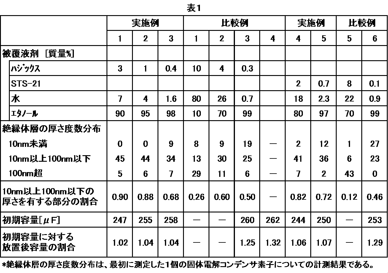
- Table 1 shows the thickness frequency distribution of the insulator layer of one solid electrolytic capacitor element measured first. In all of the 10 solid electrolytic capacitor element insulator layers, the ratio of the portion having a thickness of 10 nm or more and 100 nm or less was 2/3 or more based on the whole insulator layer. For the remaining 30 solid electrolytic capacitor elements, the capacity at 120 Hz was measured, and the average value (initial capacity) was calculated. Next, the 30 solid electrolytic capacitor elements were left in an air atmosphere at 125 ° C. for 5 days. Then, the capacity
- Comparative Examples 1 to 3 40 solid electrolytic capacitor elements were produced in the same manner as in Example 1 except that the coating liquid having the formulation shown in Table 1 was used.
- the solid electrolytic capacitor element was evaluated by the same method as in Example 1. The results are shown in Table 1. In Comparative Examples 1 and 2, the ESR was too large to measure the capacity.
- Comparative Example 4 40 solid electrolytic capacitor elements were produced by the same method as in Example 1 except that the insulator layer was not provided.
- the solid electrolytic capacitor element was evaluated by the same method as in Example 1. The results are shown in Table 1.
- Example 4 The coating liquid used in Example 1 was changed to a coating liquid prepared by mixing 2% by mass of titania nanoparticle liquid (“STS-21” manufactured by Ishihara Sangyo Co., Ltd.), 18% by mass of water and 80% by mass of ethanol. Produced 40 solid electrolytic capacitor elements in the same manner as in Example 1. The solid electrolytic capacitor element was evaluated by the same method as in Example 1. The results are shown in Table 1.
- Example 5 and Comparative Examples 5-6 40 solid electrolytic capacitor elements were produced in the same manner as in Example 4 except that the coating liquid having the formulation shown in Table 1 was used.
- the solid electrolytic capacitor element was evaluated by the same method as in Example 1. The results are shown in Table 1. In Comparative Example 5, the ESR was too large to measure the capacity.
- Example 6 500 g of tungsten raw material powder obtained by the same method as in Example 1 and 1500 g of water were placed in a 2 L beaker and stirred at 100 rpm for 5 minutes. When 10 seconds had passed since the stirring was stopped, particles floating in the liquid were sucked together with water with a syringe. The sucked particles were vacuum-dried at 80 ° C. The dried product was crushed in a mortar at room temperature to obtain 96 g of powder. The powder had a number average primary particle size of 0.25 ⁇ m as measured by observation with an electron microscope. To this powder, 0.2% by mass of a crystalline silicon powder having a 50% particle size of 1 ⁇ m was added to obtain a mixed powder. This was left for 30 minutes at 1430 ° C.
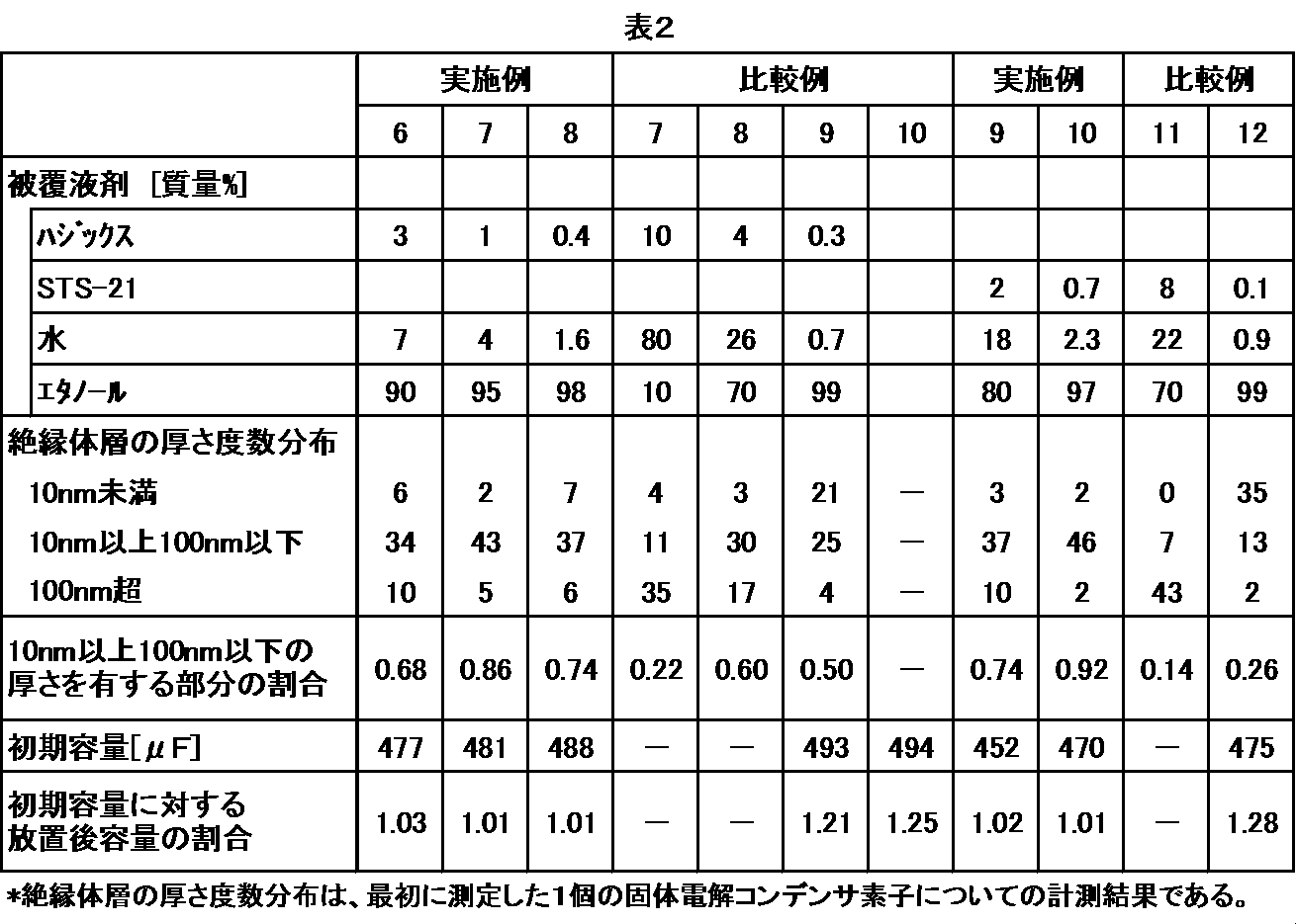
- Example 2 a sintered body (powder mass 55 mg, BET specific surface area 1.3 m 2 / g) was produced in the same manner as in Example 1. Subsequently, in the same manner as in Example 1, a dielectric layer, a semiconductor layer, an insulator layer, a carbon layer and a silver layer were provided, and 40 solid electrolytic capacitor elements were produced. The solid electrolytic capacitor element was evaluated by the same method as in Example 1. The results are shown in Table 2.
- Examples 7-8, Comparative Examples 7-9 40 solid electrolytic capacitor elements were produced in the same manner as in Example 6 except that the coating liquid having the formulation shown in Table 2 was used.
- the solid electrolytic capacitor element was evaluated by the same method as in Example 1. In Comparative Examples 7 and 8, the ESR was too large to measure the capacity. The results are shown in Table 2.
- Comparative Example 10 40 solid electrolytic capacitor elements were produced in the same manner as in Example 6 except that the insulator layer was not provided.
- the solid electrolytic capacitor element was evaluated by the same method as in Example 1. The results are shown in Table 2.
- Example 9 The same as in Example 6 except that the coating solution was changed to a coating solution prepared by mixing 2% by mass of the titania nanoparticle solution “STS-21” manufactured by Ishihara Sangyo Co., Ltd., 18% by mass of water and 80% by mass of ethanol. 40 solid electrolytic capacitor elements were produced by this method. The solid electrolytic capacitor element was evaluated by the same method as in Example 1. The results are shown in Table 2.
- Example 10 and Comparative Examples 11-12 40 solid electrolytic capacitor elements were produced in the same manner as in Example 9 except that the coating liquid having the formulation shown in Table 2 was used.
- the solid electrolytic capacitor element was evaluated by the same method as in Example 1. In Comparative Example 11, the ESR was too large to measure the capacity. The results are shown in Table 2.
Landscapes
- Engineering & Computer Science (AREA)
- Power Engineering (AREA)
- Microelectronics & Electronic Packaging (AREA)
- Chemical & Material Sciences (AREA)
- Materials Engineering (AREA)
- Manufacturing & Machinery (AREA)
- Electric Double-Layer Capacitors Or The Like (AREA)
Abstract
Description
前記絶縁体層は、10nm以上100nm以下の厚さを有する部分の割合が、絶縁体層全体を基準にして、2/3以上である、固体電解コンデンサ素子。
〔3〕前記絶縁体層が無機酸化物からなるものである〔1〕に記載の固体電解コンデンサ素子。
〔4〕前記無機酸化物が、二酸化ケイ素、二酸化チタン、酸化ジルコニウムおよび酸化ハフニウムからなる群より選ばれる少なくとも一つを含むものである〔3〕に記載の固体電解コンデンサ素子。
〔5〕前記絶縁体層が、平均粒子径1nm~90nmのナノ粒子からなるものである〔1〕~〔4〕のいずれかひとつに記載の固体電解コンデンサ素子。
〔6〕前記カーボン層が有機溶媒系カーボンペーストを用いて形成されたものである〔1〕~〔5〕のいずれかひとつに記載の固体電解コンデンサ素子。
〔7〕前記陽極体がタングステンからなるものである〔1〕~〔6〕のいずれかに記載の固体電解コンデンサ素子。
〔8〕〔1〕~〔7〕のいずれかひとつに記載の固体電解コンデンサ素子を含む固体電解コンデンサ。
陽極体を覆うように誘電体層を形成し、
誘電体層の上に半導体層を形成し、
半導体層の上に、絶縁体粒子の分散液を、得られる絶縁体層において10nm以上100nm以下の厚さを有する部分の割合が絶縁体層全体を基準にして2/3以上となるように、被覆することによって、絶縁体層を形成し、
絶縁体層の上にカーボン層を形成し、次いで
カーボン層の上に銀層を形成することを含む、
固体電解コンデンサ素子の製造方法。
原料としての弁作用金属粉は、その体積基準累積粒度分布における50%粒子径が好ましくは0.1~1μm、より好ましくは0.1~0.7μm、さらに好ましくは0.1~0.3μmである。弁作用金属粉は造粒粉であってもよい。造粒粉は原料金属粉を焼成・粉砕するなどして製造することができる。造粒粉の体積基準累積粒度分布における50%粒子径は、好ましくは20~170μm、より好ましくは26~140μmである。造粒粉は原料金属粉が焼結して成る多孔質粉であることが好ましい。なお、50%粒子径は、マイクロトラック社製 HRA 9320-X100などを用い、レーザー回折散乱法で体積基準粒度分布を測定して算出することができる。
絶縁体層の厚さや層構造は被覆液中に含まれるナノ粒子の濃度や被覆液の被覆処理回数などによって調整できる。絶縁体層は、厚すぎると電気抵抗が増大し、薄すぎると効果が少ない。
固体電解コンデンサ素子の破断面試料を用意し、その断面の走査型電子顕微鏡(SEM)にて100,000倍の画像を得た。1試料につき、10μm四方の視野において無作為に50か所の絶縁体層の厚さを計測した。計測データを10nm未満、10nm以上100nm以下、および100nm超に区分した。10試料についての計測データを取りまとめ、10nm以上100nm以下の範囲に区分けされたデータ度数の割合を算出した。
恒温乾燥器を用い、100℃の空気中で5分間固体電解コンデンサ素子を乾燥させた。その直後にLCR測定器に配線された導線をコンデンサ素子の陰極層とコンデンサ素子に植立した陽極リード線に当てた。バイアス電圧2.5Vにて、120Hzにおける容量を、アジレント社製LCR測定器で測定した。無作為に選んだコンデンサ素子30個の測定値の平均値を算出した。
マイクロトラック社製 HRA 9320-X100を用い、レーザー回折散乱法で粒度分布を測定し、体積基準累積粒度分布における50%粒子径(D50)、10%粒子径(D10)及び90%粒子径(D90)を求めた。D10からD90の範囲を「粒径レンジ」と定義した。
ICP発光分析によって陽極体中の元素含有量を決定した。また、酸素・窒素分析装置(LECO社製TC600)を用いて陽極体中の窒素量と酸素量をそれぞれ熱伝導度法と赤外吸収法により決定した。無作為に選択した陽極体2個の平均値を算出した。
三酸化タングステン粉を水素還元して50%粒子径0.5μm(粒径レンジ0.08μm~20μm)のタングステン原料粉を得た。これを真空下1430℃で30分間放置して塊状物を得た。該塊状物を室温で瑪瑙鉢にて解砕し、50%粒子径76μm(粒径レンジ26~180μm、嵩比重3.2g/cm3、酸素含有量4800質量ppm、窒素含有量550質量ppm、BET比表面積0.76m2/g)の造粒粉を得た。
この造粒粉を圧し固めて成形体を得た。この成形体を真空下1500℃にて20分間焼成して、1.0mm×1.5mm×4.5mmの焼結体(粉質量61mg、BET比表面積0.53m2/g)を作製した。なお、焼結体の1.0×1.5mm面の中央に、陽極リード線となる直径0.29mmのタンタル線を植立させた。
続いて、3質量%過硫酸アンモニウム水溶液(化成液)に浸漬して、23℃にて、焼結体1個あたり0.5mAの初期電流密度で電解酸化を開始、電圧が7Vに達した時から7Vに維持して15分間電解酸化(後化成)を行った。
被覆液剤に、半導体層が形成された焼結体を陽極リード線の付根まで浸漬した。被覆液剤から焼結体を引き上げて、105℃にて15分間乾燥させて、半導体層の上にシリコーンナノ粒子からなる絶縁体層を設けた。
次いで、銀ペースト液にカーボン層が設けられた焼結体を陽極リード線の植立した面が浸らない位置まで浸漬し、銀ペースト液から引き上げて乾燥させて、カーボン層の上に銀層を設けた。
以上の操作により40個の固体電解コンデンサ素子を作製した。
残された固体電解コンデンサ素子30個について、120Hzでの容量を測定し、その平均値(初期容量)を算出した。次いで、該固体電解コンデンサ素子30個を125℃の空気雰囲気に5日間放置した。その後、120Hzでの容量を測定し、その平均値(放置後容量)を算出した。その結果を表1に示す。
表1に示す処方の被覆液剤に変えた以外は実施例1と同じ方法で固体電解コンデンサ素子40個を作製した。該固体電解コンデンサ素子について実施例1と同じ方法で評価した。その結果を表1に示す。なお、比較例1および2ではESRが大きくなりすぎ容量の測定ができなかった。
絶縁体層を設けなかった以外は実施例1と同じ方法で固体電解コンデンサ素子40個を作製した。該固体電解コンデンサ素子について実施例1と同じ方法で評価した。その結果を表1に示す。
実施例1で用いた被覆液剤を、チタニアナノ粒子液剤(石原産業株式会社製「STS-21」)2質量%、水18質量%およびエタノール80質量%を混ぜ合わせて調製した被覆液剤に変えた以外は、実施例1と同じ方法で固体電解コンデンサ素子40個を作製した。該固体電解コンデンサ素子について実施例1と同じ方法で評価した。その結果を表1に示す。
表1に示す処方の被覆液剤に変えた以外は実施例4と同じ方法で固体電解コンデンサ素子40個を作製した。該固体電解コンデンサ素子について実施例1と同じ方法で評価した。その結果を表1に示す。なお、比較例5ではESRが大きくなりすぎ容量の測定ができなかった。
実施例1と同じ方法で得たタングステン原料粉500g、および水1500gを2Lのビーカーに入れ、100rpmで5分間撹拌した。撹拌停止から10秒経過した時に液中に漂う粒子を水とともに注射器で吸い込んだ。吸い込んだ粒子を80℃で真空乾燥させた。乾燥物を室温にて瑪瑙鉢で解砕して粉末96gを得た。該粉末は、電子顕微鏡観察による測定で数平均一次粒子径が0.25μmであった。この粉末に50%粒子径1μmの結晶ケイ素粉を0.2質量%加えて、混合粉を得た。これを真空下1430℃で30分間放置して塊状物を得た。該塊状物を室温で瑪瑙鉢にて解砕して、造粒粉を得た。造粒粉は、ICP発光分析による元素分析から、0.2質量%のケイ素を含んでいることが確認された。
該造粒粉を用いて、実施例1と同じ方法で、焼結体(粉質量55mg、BET比表面積1.3m2/g)を作製した。
続いて実施例1と同じ方法にて、誘電体層、半導体層、絶縁体層、カーボン層および銀層をそれぞれ設けて、固体電解コンデンサ素子40個を作製した。該固体電解コンデンサ素子について実施例1と同じ方法で評価した。その結果を表2に示す。
表2に示す処方の被覆液剤に変えた以外は実施例6と同じ方法で固体電解コンデンサ素子40個を作製した。該固体電解コンデンサ素子について実施例1と同じ方法で評価した。比較例7および8ではESRが大きくなりすぎ容量の測定ができなかった。その結果を表2に示す。
絶縁体層を設けなかった以外は実施例6と同じ方法で固体電解コンデンサ素子40個を作製した。該固体電解コンデンサ素子について実施例1と同じ方法で評価した。その結果を表2に示す。
被覆液剤を、石原産業株式会社製のチタニアナノ粒子液剤「STS-21」2質量%、水18質量%およびエタノール80質量%を混ぜ合わせて調製した被覆液剤に変えた以外は、実施例6と同じ方法で固体電解コンデンサ素子40個を作製した。該固体電解コンデンサ素子について実施例1と同じ方法で評価した。その結果を表2に示す。
表2に示す処方の被覆液剤に変えた以外は実施例9と同じ方法で固体電解コンデンサ素子40個を作製した。該固体電解コンデンサ素子について実施例1と同じ方法で評価した。比較例11ではESRが大きくなりすぎ容量の測定ができなかった。その結果を表2に示す。
Claims (9)
- 陽極体、 該陽極体を覆うように設けられた誘電体層、 該誘電体層の上に設けられた半導体層、 該半導体層の上に設けられた絶縁体層、 該絶縁体層の上に設けられたカーボン層、および 該カーボン層の上に設けられた銀層を有し、且つ
前記絶縁体層は、10nm以上100nm以下の厚さを有する部分の割合が、絶縁体層全体を基準にして、2/3以上である、
固体電解コンデンサ素子。 - 前記絶縁体層がシリコーンからなるものである請求項1に記載の固体電解コンデンサ素子。
- 前記絶縁体層が無機酸化物からなるものである請求項1に記載の固体電解コンデンサ素子。
- 前記無機酸化物が、二酸化ケイ素、二酸化チタン、酸化ジルコニウムおよび酸化ハフニウムからなる群より選ばれる少なくとも一つを含むものである請求項3に記載の固体電解コンデンサ素子。
- 前記絶縁体層が、平均粒子径1nm~90nmのナノ粒子からなるものである請求項1~4のいずれかひとつに記載の固体電解コンデンサ素子。
- 前記カーボン層が有機溶媒系カーボンペーストを用いて形成されたものである請求項1~5のいずれかひとつに記載の固体電解コンデンサ素子。
- 前記陽極体がタングステンからなるものである請求項1~6のいずれかに記載の固体電解コンデンサ素子。
- 請求項1~7のいずれかひとつに記載の固体電解コンデンサ素子を含む固体電解コンデンサ。
- 陽極体を用意し、
陽極体を覆うように誘電体層を形成し、
誘電体層の上に半導体層を形成し、
半導体層の上に、絶縁体粒子の分散液を、得られる絶縁体層において10nm以上100nm以下の厚さを有する部分の割合が絶縁体層全体を基準にして2/3以上となるように、被覆することによって、絶縁体層を形成し、
絶縁体層層の上にカーボン層を形成し、次いで
カーボン層の上に銀層を形成することを含む、
固体電解コンデンサ素子の製造方法。
Priority Applications (2)
| Application Number | Priority Date | Filing Date | Title |
|---|---|---|---|
| JP2015530973A JP6400584B2 (ja) | 2013-08-09 | 2014-08-08 | 固体電解コンデンサ素子 |
| US14/910,723 US9922772B2 (en) | 2013-08-09 | 2014-08-08 | Solid electrolytic capacitor element |
Applications Claiming Priority (2)
| Application Number | Priority Date | Filing Date | Title |
|---|---|---|---|
| JP2013-166159 | 2013-08-09 | ||
| JP2013166159 | 2013-08-09 |
Publications (1)
| Publication Number | Publication Date |
|---|---|
| WO2015020185A1 true WO2015020185A1 (ja) | 2015-02-12 |
Family
ID=52461509
Family Applications (1)
| Application Number | Title | Priority Date | Filing Date |
|---|---|---|---|
| PCT/JP2014/070978 Ceased WO2015020185A1 (ja) | 2013-08-09 | 2014-08-08 | 固体電解コンデンサ素子 |
Country Status (3)
| Country | Link |
|---|---|
| US (1) | US9922772B2 (ja) |
| JP (1) | JP6400584B2 (ja) |
| WO (1) | WO2015020185A1 (ja) |
Citations (5)
| Publication number | Priority date | Publication date | Assignee | Title |
|---|---|---|---|---|
| JPH1050561A (ja) * | 1996-07-31 | 1998-02-20 | Hitachi Aic Inc | 固体電解コンデンサ |
| JP2008198681A (ja) * | 2007-02-09 | 2008-08-28 | Matsushita Electric Ind Co Ltd | 固体電解コンデンサおよびその製造方法 |
| JP2009224568A (ja) * | 2008-03-17 | 2009-10-01 | Hitachi Aic Inc | 固体電解コンデンサの製造方法 |
| JP2009239145A (ja) * | 2008-03-28 | 2009-10-15 | Nippon Chemicon Corp | 固体電解コンデンサ及びその製造方法 |
| JP2012129293A (ja) * | 2010-12-14 | 2012-07-05 | Sanyo Electric Co Ltd | 固体電解コンデンサおよびその製造方法 |
Family Cites Families (7)
| Publication number | Priority date | Publication date | Assignee | Title |
|---|---|---|---|---|
| JP4100854B2 (ja) | 1999-03-05 | 2008-06-11 | 三洋電機株式会社 | 固体電解コンデンサの製造方法 |
| JP2006005233A (ja) * | 2004-06-18 | 2006-01-05 | Shinko Electric Ind Co Ltd | キャパシタ、キャパシタ内蔵基板、およびキャパシタの製造方法 |
| US20070171596A1 (en) * | 2006-01-20 | 2007-07-26 | Chacko Antony P | Electrode compositions containing carbon nanotubes for solid electrolyte capacitors |
| US8310816B2 (en) * | 2009-05-21 | 2012-11-13 | Kemet Electronics Corporation | Solid electrolytic capacitors with improved reliability |
| US9190214B2 (en) * | 2009-07-30 | 2015-11-17 | Kemet Electronics Corporation | Solid electrolytic capacitors with improved ESR stability |
| JP5778450B2 (ja) * | 2010-04-22 | 2015-09-16 | ローム株式会社 | 固体電解コンデンサおよび固体電解コンデンサの製造方法 |
| TWI532783B (zh) * | 2013-05-20 | 2016-05-11 | 長興材料工業股份有限公司 | 導電性材料調配物及其用途 |
-
2014
- 2014-08-08 JP JP2015530973A patent/JP6400584B2/ja not_active Expired - Fee Related
- 2014-08-08 US US14/910,723 patent/US9922772B2/en not_active Expired - Fee Related
- 2014-08-08 WO PCT/JP2014/070978 patent/WO2015020185A1/ja not_active Ceased
Patent Citations (5)
| Publication number | Priority date | Publication date | Assignee | Title |
|---|---|---|---|---|
| JPH1050561A (ja) * | 1996-07-31 | 1998-02-20 | Hitachi Aic Inc | 固体電解コンデンサ |
| JP2008198681A (ja) * | 2007-02-09 | 2008-08-28 | Matsushita Electric Ind Co Ltd | 固体電解コンデンサおよびその製造方法 |
| JP2009224568A (ja) * | 2008-03-17 | 2009-10-01 | Hitachi Aic Inc | 固体電解コンデンサの製造方法 |
| JP2009239145A (ja) * | 2008-03-28 | 2009-10-15 | Nippon Chemicon Corp | 固体電解コンデンサ及びその製造方法 |
| JP2012129293A (ja) * | 2010-12-14 | 2012-07-05 | Sanyo Electric Co Ltd | 固体電解コンデンサおよびその製造方法 |
Also Published As
| Publication number | Publication date |
|---|---|
| JPWO2015020185A1 (ja) | 2017-03-02 |
| US20160189873A1 (en) | 2016-06-30 |
| US9922772B2 (en) | 2018-03-20 |
| JP6400584B2 (ja) | 2018-10-03 |
Similar Documents
| Publication | Publication Date | Title |
|---|---|---|
| Liu et al. | Hybrid nanowires and nanoparticles of WO 3 in a carbon aerogel for supercapacitor applications | |
| CN100490035C (zh) | 电解电容及其制造方法 | |
| DE102012221861A1 (de) | Flüssigelektrolytkondensator, der einen gelierten Arbeitselektrolyten enthält | |
| JP5698882B1 (ja) | コンデンサ陽極体およびその製造方法 | |
| Liu et al. | Porous Ag-doped MnO2 thin films for supercapacitor electrodes | |
| EP1344750A1 (en) | Method of forming titanium oxide film and titanium electrolytic capacitor | |
| US9607770B2 (en) | Method for producing capacitor | |
| JP5851667B1 (ja) | コンデンサ陽極体、固体電解コンデンサ素子、固体電解コンデンサおよびコンデンサ陽極体の製造方法 | |
| JP5731719B2 (ja) | カーボンペーストおよび固体電解コンデンサ素子 | |
| CN102473528B (zh) | 固体电解电容器的制造方法 | |
| JP6400584B2 (ja) | 固体電解コンデンサ素子 | |
| WO2014119312A1 (ja) | 固体電解コンデンサおよびその製造方法 | |
| JP4986272B2 (ja) | ニオブ粉、その焼結体及びコンデンサ | |
| JP5476511B1 (ja) | コンデンサ素子 | |
| Guo et al. | Ag/MnO2 nanorod as electrode material for high-performance electrochemical supercapacitors | |
| KR102119411B1 (ko) | 다공성 복합체 전극의 제조방법 및 다공성 복합체 전극의 유기물 제거방법 | |
| JP4554063B2 (ja) | チタン酸化被膜の形成方法およびチタン電解コンデンサ | |
| JP5840821B1 (ja) | タングステンコンデンサ素子及びその製造方法 | |
| WO2026070610A1 (ja) | コンデンサ | |
| Chen et al. | Structure and Manufacturing Process of MnO2 Counter Electrode in Niobium Suboxide Capacitors | |
| JP2009231320A (ja) | 固体電解コンデンサおよびその製造方法 | |
| Whitman et al. | Electrochemical Storage in Zr-W Mixed Oxide Nanostructured Arrays | |
| Chen et al. | Supercapacitor Fabrication by Titanium Alloy | |
| JP2002249865A (ja) | チタン酸化被膜の形成方法およびチタン電解コンデンサ | |
| JP2002180293A (ja) | チタン酸化被膜の形成方法およびチタン電解コンデンサ |
Legal Events
| Date | Code | Title | Description |
|---|---|---|---|
| 121 | Ep: the epo has been informed by wipo that ep was designated in this application |
Ref document number: 14833924 Country of ref document: EP Kind code of ref document: A1 |
|
| ENP | Entry into the national phase |
Ref document number: 2015530973 Country of ref document: JP Kind code of ref document: A |
|
| WWE | Wipo information: entry into national phase |
Ref document number: 14910723 Country of ref document: US |
|
| NENP | Non-entry into the national phase |
Ref country code: DE |
|
| 122 | Ep: pct application non-entry in european phase |
Ref document number: 14833924 Country of ref document: EP Kind code of ref document: A1 |