WO2015019644A1 - 電子部品およびその製造方法 - Google Patents
電子部品およびその製造方法 Download PDFInfo
- Publication number
- WO2015019644A1 WO2015019644A1 PCT/JP2014/055260 JP2014055260W WO2015019644A1 WO 2015019644 A1 WO2015019644 A1 WO 2015019644A1 JP 2014055260 W JP2014055260 W JP 2014055260W WO 2015019644 A1 WO2015019644 A1 WO 2015019644A1
- Authority
- WO
- WIPO (PCT)
- Prior art keywords
- electronic component
- base
- external electrode
- insulating
- side surfaces
- Prior art date
- Legal status (The legal status is an assumption and is not a legal conclusion. Google has not performed a legal analysis and makes no representation as to the accuracy of the status listed.)
- Ceased
Links
Images








Classifications
-
- H—ELECTRICITY
- H01—ELECTRIC ELEMENTS
- H01G—CAPACITORS; CAPACITORS, RECTIFIERS, DETECTORS, SWITCHING DEVICES, LIGHT-SENSITIVE OR TEMPERATURE-SENSITIVE DEVICES OF THE ELECTROLYTIC TYPE
- H01G2/00—Details of capacitors not covered by a single one of groups H01G4/00-H01G11/00
- H01G2/10—Housing; Encapsulation
-
- H—ELECTRICITY
- H01—ELECTRIC ELEMENTS
- H01C—RESISTORS
- H01C1/00—Details
- H01C1/02—Housing; Enclosing; Embedding; Filling the housing or enclosure
- H01C1/028—Housing; Enclosing; Embedding; Filling the housing or enclosure the resistive element being embedded in insulation with outer enclosing sheath
-
- H—ELECTRICITY
- H01—ELECTRIC ELEMENTS
- H01C—RESISTORS
- H01C1/00—Details
- H01C1/02—Housing; Enclosing; Embedding; Filling the housing or enclosure
- H01C1/034—Housing; Enclosing; Embedding; Filling the housing or enclosure the housing or enclosure being formed as coating or mould without outer sheath
-
- H—ELECTRICITY
- H01—ELECTRIC ELEMENTS
- H01C—RESISTORS
- H01C7/00—Non-adjustable resistors formed as one or more layers or coatings; Non-adjustable resistors made from powdered conducting material or powdered semi-conducting material with or without insulating material
- H01C7/18—Non-adjustable resistors formed as one or more layers or coatings; Non-adjustable resistors made from powdered conducting material or powdered semi-conducting material with or without insulating material comprising a plurality of layers stacked between terminals
-
- H—ELECTRICITY
- H01—ELECTRIC ELEMENTS
- H01G—CAPACITORS; CAPACITORS, RECTIFIERS, DETECTORS, SWITCHING DEVICES, LIGHT-SENSITIVE OR TEMPERATURE-SENSITIVE DEVICES OF THE ELECTROLYTIC TYPE
- H01G4/00—Fixed capacitors; Processes of their manufacture
- H01G4/002—Details
- H01G4/224—Housing; Encapsulation
-
- H—ELECTRICITY
- H01—ELECTRIC ELEMENTS
- H01G—CAPACITORS; CAPACITORS, RECTIFIERS, DETECTORS, SWITCHING DEVICES, LIGHT-SENSITIVE OR TEMPERATURE-SENSITIVE DEVICES OF THE ELECTROLYTIC TYPE
- H01G4/00—Fixed capacitors; Processes of their manufacture
- H01G4/002—Details
- H01G4/228—Terminals
- H01G4/232—Terminals electrically connecting two or more layers of a stacked or rolled capacitor
-
- H—ELECTRICITY
- H01—ELECTRIC ELEMENTS
- H01G—CAPACITORS; CAPACITORS, RECTIFIERS, DETECTORS, SWITCHING DEVICES, LIGHT-SENSITIVE OR TEMPERATURE-SENSITIVE DEVICES OF THE ELECTROLYTIC TYPE
- H01G4/00—Fixed capacitors; Processes of their manufacture
- H01G4/30—Stacked capacitors
-
- H—ELECTRICITY
- H01—ELECTRIC ELEMENTS
- H01C—RESISTORS
- H01C7/00—Non-adjustable resistors formed as one or more layers or coatings; Non-adjustable resistors made from powdered conducting material or powdered semi-conducting material with or without insulating material
- H01C7/02—Non-adjustable resistors formed as one or more layers or coatings; Non-adjustable resistors made from powdered conducting material or powdered semi-conducting material with or without insulating material having positive temperature coefficient
-
- H—ELECTRICITY
- H01—ELECTRIC ELEMENTS
- H01C—RESISTORS
- H01C7/00—Non-adjustable resistors formed as one or more layers or coatings; Non-adjustable resistors made from powdered conducting material or powdered semi-conducting material with or without insulating material
- H01C7/04—Non-adjustable resistors formed as one or more layers or coatings; Non-adjustable resistors made from powdered conducting material or powdered semi-conducting material with or without insulating material having negative temperature coefficient
Definitions
- the present invention relates to an electronic component in which external electrodes are formed on both ends of a substantially rectangular parallelepiped base, and a method for manufacturing the same.
- this type of electronic component is used in, for example, a surface-mounted crystal oscillator (hereinafter simply referred to as a crystal oscillator) as described in Patent Document 1.
- a crystal oscillator hereinafter simply referred to as a crystal oscillator
- a conventional crystal oscillator will be described with reference to FIGS.
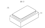
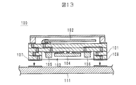
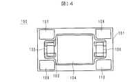
- FIGS. 12, 13 and 14 are a perspective view, a longitudinal sectional view and a bottom view of a conventional crystal oscillator 100, respectively.
- the crystal oscillator 100 includes a container body 101 having a substantially rectangular parallelepiped shape.
- a crystal resonator 102 is mounted on the upper surface of the container body 101.
- a recess 103 is formed on the bottom surface of the container body 101.
- an IC chip 104 and electronic components 105 and 106 electrically connected thereto are mounted in the recess 103.
- the IC chip 104 and the electronic components 105 and 106 constitute a control circuit for the crystal unit 102.
- the IC chip 104 is flip-chip mounted in the recess 103.
- the electronic components 105 and 106 are mounted in the recess 103 using external electrodes formed at both ends of the ceramic substrate.
- External terminal electrodes 107 to 110 are formed at the four corners of the bottom surface of the container body 101.
- the external terminal electrodes 107 to 110 are electrically connected to the IC chip 104 and the electronic components 105 and 106 via various conductors (via conductors and planar conductor patterns) formed inside the container body 101.
- the external terminal electrodes 107 to 110 are used when the crystal oscillator 100 is joined to a printed wiring board (hereinafter referred to as PCB) 111 which is a main substrate larger than the crystal oscillator 100 by soldering.
- PCB printed wiring board
- the crystal oscillator 100 is required to be further downsized.
- the recess 103 may become smaller in the height direction, left-right direction, and front-rear direction.
- the concave portion 103 when the concave portion 103 is reduced, when the crystal oscillator 100 is mounted on the PCB 111, the external electrodes of the electronic components 105 and 106 are connected to the wiring pattern on the PCB 111 side due to factors such as displacement and dimensional tolerance. Or the land electrode may be unnecessarily contacted.
- the IC chip 104 cannot control the crystal resonator 102 correctly.
- the case where the electronic components 105 and 106 are applied to the crystal oscillator 100 has been described. However, the above problems can occur in other applications.
- an object of the present invention is to provide an electronic component capable of preventing unnecessary electrical connection of external electrodes, and a method for manufacturing the same.
- one aspect of the present invention is an electronic component, which is a third side connecting the first side surface and the second side surface substantially perpendicular to the first direction and the first side surface and the second side surface.
- a first external electrode formed on the first side surface, on the third side to the sixth side surface and in the vicinity of the first side surface, and the second side surface;
- a second external electrode formed on a side surface, a portion on the third to sixth side surfaces and in the vicinity of the second side surface, and formed on the fifth side surface in the first and second external electrodes.
- an insulating cover that covers the portion formed on the first to fourth side surfaces and in the vicinity of the fifth side surface.
- a second aspect of the present invention is a method for manufacturing an electronic component, wherein the first side surface and the second side surface substantially orthogonal to the first direction, and the third to sixth side surfaces connecting the first side surface and the second side surface.
- a first external electrode formed on the first side surface, on the third to sixth side surfaces and in the vicinity of the first side surface, and the second side A step of generating a side surface and a second external electrode formed on the third to sixth side surfaces and in the vicinity of the second side surface, and in the first and second external electrodes, Forming an insulating cover that covers a portion formed on the fifth side surface and a portion formed on the first to fourth side surfaces and in the vicinity of the fifth side surface.
- the electronic component according to each aspect described above by providing the insulating cover, it is possible to provide an electronic component capable of preventing unnecessary electrical connection between the first external electrode and the second external electrode.
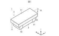
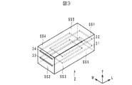
- FIG. 1 is an external perspective view of an electronic component according to a first embodiment of the present invention. It is a disassembled perspective view of the electronic component shown in FIG. It is a perspective view of the ceramic base
- FIG. 2 is a longitudinal sectional view of a cross section of the electronic component taken along the alternate long and short dash line AA ′ shown in FIG. It is a schematic diagram which shows the arrangement
- FIG. 1 shows the other structural example of the main body shown in FIG.
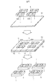
- FIG. 1 shows the 1st modification of the insulating cover shown in FIG. 1, and its manufacturing process.
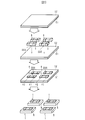
- FIG. 1 shows the 2nd modification of the insulating cover shown in FIG. 1, and its manufacturing process.
- FIG. 1 shows the 3rd modification of the insulating cover shown in FIG. 1, and its manufacturing process.
- It is a perspective view of the conventional crystal oscillator. It is a longitudinal cross-sectional view of the conventional crystal oscillator. It is a bottom view of the conventional crystal oscillator. It is a schematic diagram which shows the subject of the conventional crystal oscillator.
- the L-axis direction indicates the left-right direction of the electronic component 1 and is an example of a first direction.
- the T-axis direction indicates the vertical direction of the electronic component 1 and is an example of a second direction.
- the W-axis direction indicates the front-rear direction of the electronic component 1 and is a first example of the third direction.
- L, T, and W as reference signs are attached to the first direction, the second direction, and the third direction.
- FIG. 3 is a perspective view of the ceramic substrate 2 of the electronic component 1.
- 4 is a longitudinal sectional view of the cross section of the electronic component 1 taken along the alternate long and short dash line AA ′ shown in FIG. 1 to 4, an electronic component 1 is, for example, an NTC thermistor having a negative temperature coefficient, and includes at least a ceramic base 2, for example, two first internal electrodes 31, 32, and, for example, two sheets. Second internal electrodes 33 and 34, a first external electrode 41, a second external electrode 42, and an insulating cover 5 are provided. It should be noted that the internal electrodes 31 to 34 are not shown in FIGS. 1 and 2 but are shown by broken lines in FIG. 3 so that the illustration is not complicated.
- the substrate 2 has a substantially rectangular parallelepiped shape composed of the first side surface SS1 to the sixth side surface SS6, as clearly shown in FIG.
- the side surfaces SS1 and SS2 are, for example, the right end surface and the left end surface of the base 2 and face each other in the first direction L.
- the side surfaces SS3 and SS4 are, for example, the front surface and the back surface of the base 2 and are opposed to each other in the third direction W.
- the side surfaces SS5 and SS6 are, for example, the upper surface and the bottom surface of the base 2 and face each other in the second direction T.
- the base 2 has, for example, a 0603 size defined by the JIS standard.
- L dimension the dimension of the base 2 in the first direction L
- W dimension the dimension in the third direction W
- T dimension the dimension in the second direction T
- T dimension the dimension in the second direction T
- the base 2 is a laminate of, for example, five ceramic layers 21 to 25.
- the boundary between two ceramic layers adjacent to each other in the second direction T is virtually indicated by a two-dot chain line.
- the substrate 2 has two to four types of oxidation selected from the group including manganese (Mn), nickel (Ni), iron (Fe), cobalt (Co), copper (Cu), titanium (Ti) and the like. This is a product obtained by mixing and sintering an object (hereinafter sometimes referred to as an oxide sintered body).
- the substrate 2 has a negative temperature coefficient (B constant) determined by the composition and the like, and the resistance value decreases substantially linearly as the temperature rises within the temperature range in which the electronic component 1 is used.
- internal electrodes 31 to 34 are planar electrodes, and are produced by applying and baking a conductive paste mainly composed of silver (Ag) -palladium (Pd).
- the internal electrode 31 is between the ceramic layers 21 and 22, the internal electrode 32 is between the ceramic layers 23 and 24, the internal electrode 33 is between the ceramic layers 22 and 23, and the internal electrode 34 is between the ceramic layers 24 and 25. Intervene in.
- Each of these internal electrodes 31 to 34 has a rectangular shape in plan view from the second direction T.
- the internal electrodes 31 to 33 will be described more specifically.
- the internal electrodes 31 and 32 extend from the side surface SS1 of the base 2 on the thermistor layers 21 and 23 in the direction opposite to the first direction L. Further, the internal electrodes 31 and 32 are exposed from the side surface SS1 of the base 2 for electrical connection with the external electrode 41 described later, but the other portions are covered with the base 2.
- the internal electrodes 33 and 34 extend in the first direction L on the ceramic layers 22 and 24 from the side surface SS2 of the base 2. Further, the internal electrodes 33 and 34 are exposed from the base 2 at the side surface SS2 for electrical connection with the external electrode 42 described later, but the other portions are covered by the base 2.
- Each of the external electrodes 41 and 42 includes a base layer mainly composed of Ag, a nickel (Ni) plating layer formed on the base layer, and a tin (Sn) plating layer formed on the Ni plating layer. , Including.
- the external electrode 41 is provided so as to cover the right end portion of the base 2. More specifically, it is formed so as to cover the entire side surface SS1 and the right end portion of the side surfaces SS3 to SS6 (see FIG. 3) (that is, the portion in the vicinity of the side surface SS1). Further, as described above, the external electrode 41 is electrically connected to the internal electrodes 31 and 32.
- the external electrode 42 is provided so as to cover the left end portion of the base 2 and not to contact the external electrode 41. More specifically, it is formed so as to cover the entire side surface SS2 and the left end portion of the side surfaces SS3 to SS6 (see FIG. 3) (that is, the portion near the side surface SS2). Further, as described above, the external electrode 42 is electrically connected to the internal electrodes 33 and 34.
- the electronic component 1 a portion composed of the base 2, the internal electrodes 31 to 34, and the external electrodes 41 and 42 is shown in FIG.
- the main body 6 is called.
- the insulating cover 5 is a plate-like member having a rectangular shape in plan view from the second direction T, and generally covers the upper end portion of the main body 6.
- the L dimension is about 1.0 [mm] and the W dimension is about 0.5 [mm].
- the T dimension should just be more than 0 [mm] and less than 0.15 [mm].
- the insulating cover 5 covers the side surface SS5 (see FIG. 3) of the base 2 and the portions formed on the side surface SS5 in both the external electrodes 41 and 42, and the upper end portions of the side surfaces SS1 to SS5 of the base 2;
- the external electrodes 41 and 42 cover portions formed on the upper end portions of the side surfaces SS1 to SS5.
- the outline of the insulating cover 5 is the outline of the base 2 and the external electrodes 41 and 42 (shown by broken lines) in plan view from the second direction T.
- the outline of the insulating cover 5 intersects and overlaps the outline of the base 2 and the external electrodes 41 and 42 in a plan view from the third direction W. In FIG. 5, such an overlapping portion is indicated by a one-dot chain line.
- the insulating cover 5 has a two-layer structure including a first insulating portion 51 and a second insulating portion 52 as shown in FIG.
- the boundary of the insulation parts 51 and 52 is shown with a broken line.
- the insulating parts 51 and 52 are made of different insulating materials. If a specific example is given, the insulating part 51 will consist of a polyimide resin sheet, for example, and the insulating part 52 will consist of an epoxy resin, for example.
- the L dimension is, for example, about 1.0 [mm]
- the W dimension is, for example, about 0.5 [mm]
- the T dimension is, for example, about 0.15 [mm] or less. is there.
- the electronic component 1 is manufactured by the following steps (1) to (8).
- the manufacturing process of the main body 6 will be described in the following (1) to (5).
- a manufacturing process of one main body 6 will be described, but a large number of main bodies 6 are actually manufactured in a lump.
- the manufacturing process of the insulating cover 5 will be described in the following (6) to (8).
- oxides of Mn, Ni, Fe, and Ti (Mn 3 O 4 , NiO, Fe 2 O 3 , TiO 2 ) as raw materials for the base 2 satisfy the design specifications of the electronic component 1. Is weighed. The weighed raw material is sufficiently wet pulverized by a ball mill using a pulverizing medium such as zirconia. Thereafter, the pulverized raw material is calcined under conditions of 760 [° C.] for 2 hours, thereby producing a ceramic powder.
- the unfired laminate is cut such that the L dimension of the fired substrate 2 is about 0.6 [mm] and the W dimension is about 0.3 [mm].
- the cut laminate is accommodated in a zirconia basket, and then subjected to a binder removal treatment under conditions of, for example, 350 [° C.] for 2 hours, and further fired at a predetermined temperature (eg, 1100 [° C.]). Thereby, a sintered compact is obtained.
- an underlayer mainly composed of Ag is formed by dipping and is baked in an air atmosphere of about 800 [° C.]. It is formed through. Thereafter, a Ni plating layer and a Sn plating layer are formed in this order on each base layer, for example, by electrolytic barrel plating. Thereby, the external electrodes 41 and 42 are formed.
- a polyimide resin sheet to be the first insulating part 51 is prepared.
- a large number of main bodies 6 are arranged in a matrix in a large amount by, for example, a mounter mounting machine.
- each main body 6 is disposed such that each side surface SS ⁇ b> 5 is in contact with the main surface of the insulating portion 51.
- the two adjacent main bodies 6 are arranged so that an interval greater than about 0.4 [mm] is provided in the first direction L and an interval greater than about 0.2 [mm] is provided in the third direction W.
- thermosetting liquid epoxy resin to be the second insulating part 52 is prepared. Thereafter, as shown in the middle of FIG. 6, the liquid epoxy resin is poured onto the polyimide resin sheet on which the main bodies 6 are arranged. The amount to be poured at this time is such that the side surface SS6 of the base 2 and the portions formed on the side surface SS6 in the external electrodes 41 and 42 (hereinafter referred to as exposed portions) are exposed. Next, vacuum defoaming is performed on the poured liquid epoxy resin.
- the liquid epoxy resin poured onto the resin sheet is heated and cured, for example, at 150 [° C.] for 30 minutes.
- the resin sheet and the cured liquid epoxy resin are cut by a dicing saw so that the L dimension is about 1.0 [mm] and the W dimension is about 0.5 [mm], and the electronic component 1 with the insulating cover 5 is formed. Complete.
- FIG. 7 is a longitudinal sectional view showing a crystal oscillator 7 to which the electronic component 1 is applied.
- the crystal oscillator 7 is provided with a container body 701 that is generally rectangular parallelepiped and made of alumina, for example.
- a crystal resonator 702 is mounted on the upper surface of the container body 701.
- a recess 703 is formed on the bottom surface of the container body 701.
- the electronic component 1 is mounted in the recess 703 for temperature compensation of the crystal resonator 702.
- the electronic component 1 detects the ambient temperature and outputs it to the IC chip 704 for temperature compensation of the crystal resonator 702.
- a total of four external terminal electrodes are formed at the four corners of the bottom surface of the container body 701, for example.
- the external terminal electrodes 707 and 708 and the like are electrically connected to the IC chip 704 and the electronic component 1 through various conductors formed inside the container body 701.
- the external terminal electrodes 707, 708 and the like are used when the crystal oscillator 7 is joined to a printed wiring board (hereinafter referred to as PCB) 711, which is a main substrate larger than the crystal oscillator 7, by soldering.
- PCB printed wiring board
- the electronic component 1 is surface-mounted in the recess 703 using the exposed portions of the external electrodes 41 and 42 as shown in an enlarged view in the lower part of FIG.
- the insulating cover 5 faces downward and faces the PCB 711.
- the recess 703 is narrow, and there may be a case where a sufficient space cannot be secured around the electronic component 1. Even in such a case, even if a positional deviation or the like occurs when the crystal oscillator 7 is mounted on the PCB 711, the external electrode 41, 42 of the electronic component 1 is connected to the wiring pattern on the PCB 711 side because of the insulating cover 5. It is possible to prevent unnecessary conduction with the land electrode.
- the dimensions of the substrate 2 are not limited to 0603 size, and may be 3225 size, 3216 size, 2012 size, 1608 size, 1005 size, and 0402 size. The details of the 3225 size will be described on behalf of these six sizes.
- the design target value of the L dimension is, for example, 3.2 [mm]
- the design target value of the W dimension is, for example, 2.5 [mm].
- the target value of the T dimension is not particularly specified, but is preferably designed to a value different from the W dimension (for example, 1.0 [mm] or less).
- the L dimension, the W dimension, and the T dimension are not necessarily exactly the above numerical values, and have tolerances. The remaining five sizes are as shown in Table 1 below.
- the main body 6 of the electronic component 1 was demonstrated as an NTC thermistor.
- the present invention is not limited to this, and the main body 6 may be a PTC thermistor having a positive temperature coefficient, a chip inductor, a chip capacitor, a chip resistor, or the like.
- the substrate 2 has been described as a laminate of the ceramic layers 21 to 25.
- the substrate 2 is not limited to this and may be a single plate.
- a polyimide resin sheet to be the first insulating part 51 and a thermosetting liquid epoxy resin to be the second insulating part 52 are prepared. Thereafter, a liquid epoxy resin is filled on the resin sheet. Next, as shown in the second row from the top in FIG. 9, the main bodies 6 (four in the drawing) are arranged in a matrix on the liquid epoxy resin.
- each main body 6 is embedded in the liquid epoxy resin by a heating press or the like, and the liquid epoxy resin is cured. Similarly to the above, the pressure applied at this time is such that the side surface SS6 of the base 2 and the portions formed on the side surface SS6 in the external electrodes 41 and 42 are exposed.
- the insulating cover 5 includes the first insulating portion 51 and the second insulating portion 52 that are different resin materials.
- the insulating cover 5 may include an insulating cover 5a made of an insulating portion 53 made of a single resin material or the like, as shown in FIG.
- Such an electronic component 1 is manufactured by the following (6b) to (8b).
- the main bodies 6 produced by the manufacturing steps (1) to (5) are arranged in a matrix on the heat-peelable foamed adhesive sheet 54. , Pushed in a little.
- the amount of pressing is such that, for example, the side surface SS6 of the base 2 and the portions formed on the side surface SS6 in the external electrodes 41 and 42 are exposed from the insulating cover 5a after completion.
- the side surface SS6 of the base 2 and the portions formed on the side surface SS6 in the external electrodes 41 and 42 are exposed from the insulating cover 5a after completion. Furthermore, the main body 6 was pushed into the foamed adhesive sheet 54.
- the present invention is not limited to this, and as shown in FIG. 11, after completion, the main body 6 is pushed into the foamed adhesive sheet 54 to the extent that the portions formed on the side surface SS6 in the external electrodes 41 and 42 are exposed from the insulating cover 5a. It does not matter.
- the electronic component and the manufacturing method thereof according to the present invention can prevent unnecessary electrical connection of external electrodes, and are suitable for NTC thermistors, PTC thermistors, chip capacitors, chip inductors, and chip resistors.
Landscapes
- Engineering & Computer Science (AREA)
- Power Engineering (AREA)
- Microelectronics & Electronic Packaging (AREA)
- Manufacturing & Machinery (AREA)
- Physics & Mathematics (AREA)
- Electromagnetism (AREA)
- Piezo-Electric Or Mechanical Vibrators, Or Delay Or Filter Circuits (AREA)
Abstract
外部電極の不必要な電気的接続を防止可能な電子部品を提供すること。 電子部品(1)において、セラミック基体(2)は、第一側面~第六側面を有する。第一外部電極(41)は、第一側面と、第三乃至第六側面上であって第一側面近傍の部分と、に形成される。第二外部電極(42)は、第二側面と、第三乃至第六側面上であって第二側面近傍の部分とに形成される。また、絶縁カバー(5)は、第一および第二外部電極において、第五側面に形成された部分と、第一乃至第四側面上であって第五側面近傍に形成された部分と、を覆っている。
Description
本発明は、略直方体形状の基体の両端に外部電極が形成された電子部品、およびその製造方法に関する。
従来、この種の電子部品は、例えば、特許文献1に記載のような表面実装型水晶発振器(以下、単に、水晶発振器という)に用いられる。以下、図12~図14を参照して、従来の水晶発振器について説明する。
図12、図13および図14は、従来の水晶発振器100の斜視図、縦断面図および底面図である。図12~図14において、水晶発振器100は、大略的には直方体形状の容器体101を備えている。この容器体101の上面には、水晶振動子102が実装される。容器体101の底面には、凹部103が形成される。凹部103には、ICチップ104と、これと電気的に接続された電子部品105,106とが実装されている。ICチップ104および電子部品105,106は、水晶振動子102の制御回路を構成する。ここで、ICチップ104は、凹部103にフリップチップ実装される。それに対し、電子部品105,106は、セラミック基体の両端部に形成された外部電極を用いて凹部103に実装される。また、容器体101の底面の四隅には外部端子電極107~110が形成されている。外部端子電極107~110は、容器体101内部に形成された各種導体(ビア導体や平面導体パターン)を介して、ICチップ104や電子部品105,106と電気的に接続される。また、外部端子電極107~110は、水晶発振器100よりも大型の主基板となるプリント配線基板(以下、PCBという)111に、水晶発振器100を半田で接合する際に使用される。
近年の電子機器(例えば、スマートフォン)の多機能化・高機能化により、電子機器の内部には、大量の電子部品が高密度に実装されている。これに伴い、上記の水晶発振器100には更なる小型化が要求されている。この要求に応えると、凹部103が高さ方向、左右方向および前後方向に小さくなってしまう場合がある。しかし、図15に示すように、凹部103が小さくなると、水晶発振器100をPCB111に実装する際に、位置ずれや寸法公差等の要因で、電子部品105,106の外部電極がPCB111側の配線パターンやランド電極に不必要に接触してしまう可能性がある。その結果、ICチップ104が水晶振動子102を正しく制御できなくなってしまう。なお、上記では、電子部品105,106を水晶発振器100に応用した場合について説明した。しかし、上記問題点は、他の用途でも起こり得る。
それゆえに、本発明の目的は、外部電極の不必要な電気的接続を防止可能な電子部品、およびその製造方法を提供することである。
上記目的を達成するために、本発明の一局面は、電子部品であって、第一方向に略直交する第一側面および第二側面と、前記第一側面および前記第二側面を繋ぐ第三乃至第六側面と、を有する基体と、前記第一側面と、前記第三乃至第六側面上であって前記第一側面近傍の部分と、に形成された第一外部電極と、前記第二側面と、前記第三乃至第六側面上であって前記第二側面近傍の部分と、に形成された第二外部電極と、前記第一および前記第二外部電極において、前記第五側面に形成された部分と、前記第一乃至前記第四側面上であって前記第五側面近傍に形成された部分と、を覆う絶縁カバーと、を備える。
本発明の第二局面は、電子部品の製造方法であって、第一方向に略直交する第一側面および第二側面と、前記第一側面および前記第二側面を繋ぐ第三乃至第六側面と、を有する基体を作製する工程と、前記第一側面と、前記第三乃至第六側面上であって前記第一側面近傍の部分と、に形成された第一外部電極と、前記第二側面と、前記第三乃至第六側面上であって前記第二側面近傍の部分と、に形成された第二外部電極と、を生成する工程と、前記第一および前記第二外部電極において、前記第五側面に形成された部分と、前記第一乃至前記第四側面上であって前記第五側面近傍に形成された部分と、を覆う絶縁カバーを形成する工程と、を備える。
上記各局面に係る電子部品によれば、絶縁カバーが備わることにより、第一外部電極および第二外部電極の不必要な電気的接続を防止可能な電子部品を提供することが可能となる。
《第一実施形態》
以下、各図を参照して、本発明の一実施形態に係る電子部品1およびその製造方法について詳細に説明する。
以下、各図を参照して、本発明の一実施形態に係る電子部品1およびその製造方法について詳細に説明する。
まず、いくつかの図面に示されるL軸、W軸およびT軸について説明する。L軸方向は、電子部品1の左右方向を示し、第一方向の一例である。T軸方向は、電子部品1の上下方向を示し、第二方向の一例である。W軸方向は、電子部品1の前後方向を示し、第三方向の第一例である。以下、本実施形態の説明の便宜上、第一方向、第二方向および第三方向には、参照符号としてのL、T、Wが付けられる。
《実施形態》
図1,図2は、電子部品1の完成品の斜視図および分解斜視図である。また、図3は、電子部品1のセラミック基体2の透視図である。図4は、図1に示す一点鎖線A-A'に沿う電子部品1の断面を矢印Bの方向から見た縦断面図である。図1~図4において、電子部品1は、例えば、負の温度係数を有するNTCサーミスタであって、少なくとも、セラミック基体2と、例えば二枚の第一内部電極31,32と、例えば二枚の第二内部電極33,34と、第一外部電極41と、第二外部電極42と、絶縁カバー5と、を備えている。なお、図示が煩雑にならないように、各内部電極31~34は、図1,図2には示さず、図3に破線にて示されている。
図1,図2は、電子部品1の完成品の斜視図および分解斜視図である。また、図3は、電子部品1のセラミック基体2の透視図である。図4は、図1に示す一点鎖線A-A'に沿う電子部品1の断面を矢印Bの方向から見た縦断面図である。図1~図4において、電子部品1は、例えば、負の温度係数を有するNTCサーミスタであって、少なくとも、セラミック基体2と、例えば二枚の第一内部電極31,32と、例えば二枚の第二内部電極33,34と、第一外部電極41と、第二外部電極42と、絶縁カバー5と、を備えている。なお、図示が煩雑にならないように、各内部電極31~34は、図1,図2には示さず、図3に破線にて示されている。
基体2は、図3に明示するように、第一側面SS1~第六側面SS6からなる略直方体形状を有する。側面SS1,SS2は、例えば基体2の右端面、左端面であって、第一方向Lに相対向する。側面SS3,SS4は、例えば基体2の前面、背面であって、第三方向Wに相対向する。側面SS5,SS6は、例えば基体2の上面、底面であって、第二方向Tに相対向する。
また、基体2は、例えばJIS規格で規定された0603サイズを有する。具体的には、基体2の第一方向Lへの寸法(以下、L寸という)は約0.6[mm]で、第三方向Wの寸法(以下、W寸という)は約0.3[mm]で、第二方向Tの寸法(以下、T寸という)は約0.15[mm]である。なお、これら寸法値はいずれも設計目標値であって、殆どの場合、公差を持っている。
また、基体2は、図4に示すように、例えば五つのセラミック層21~25の積層体である。なお、図4では、第二方向Tに隣り合う二つのセラミック層の境界を、二点鎖線で仮想的に示している。また、基体2は、マンガン(Mn)、ニッケル(Ni)、鉄(Fe)、コバルト(Co)、銅(Cu)およびチタン(Ti)等を含むグループから選ばれた二種から四種の酸化物を混合して焼結したもの(以下、酸化物焼結体という場合がある)である。この基体2は、組成等により定まる負の温度係数(B定数)を有しており、本電子部品1が使用される温度範囲内で温度上昇に伴い抵抗値が概ねリニアに減少する。
図3,図4において、内部電極31~34は、平面電極であって、銀(Ag)-パラジウム(Pd)を主成分とする導電性ペーストを塗布し焼成することで生成される。内部電極31はセラミック層21,22の間に、内部電極32はセラミック層23,24の間に、内部電極33はセラミック層22,23の間に、内部電極34はセラミック層24,25の間に介在する。これら内部電極31~34はいずれも、第二方向Tからの平面視で矩形形状を有する。以下、各内部電極31~33について、より具体的に説明する。
内部電極31,32は、基体2の側面SS1からサーミスタ層21,23上を第一方向Lの逆方向に延在する。また、内部電極31,32は、後述の外部電極41との電気的接続のために、基体2の側面SS1から露出しているが、それ以外の部分は基体2で覆われている。
内部電極33,34は、基体2の側面SS2からセラミック層22,24上を第一方向Lに延在する。また、内部電極33,34は、後述の外部電極42との電気的接続のために、側面SS2で基体2から露出しているが、それ以外の部分は基体2で覆われている。
次に、図2,図4を参照する。外部電極41,42はそれぞれ、Agを主成分とする下地層と、下地層上に形成されたニッケル(Ni)のめっき層と、Niめっき層上に形成されたスズ(Sn)のめっき層と、を含んでいる。
外部電極41は、基体2の右端部分を覆うように設けられている。より具体的には、側面SS1全域と、側面SS3~SS6(図3参照)の右端部分(つまり、側面SS1近傍の部分)とを覆うように形成される。また、上記の通り、外部電極41は、内部電極31,32と電気的に接続される。
外部電極42は、基体2の左端部分を覆い、かつ外部電極41に接触しないように設けられている。より具体的には、側面SS2全域と、側面SS3~SS6(図3参照)の左端部分(つまり、側面SS2近傍の部分)とを覆うように形成される。また、上記の通り、外部電極42は、内部電極33,34と電気的に接続される。
ここで、以下の説明の便宜のため、電子部品1において、基体2と、内部電極31~34と、外部電極41,42と、からなる部分を、図2等に示すように、電子部品1の本体6という。
次に、図1,図2を参照する。絶縁カバー5は、第二方向Tからの平面視で矩形形状を有する板状部材であって、大略的には、本体6の上端部分を覆っている。この絶縁カバー5に関し、L寸は約1.0[mm]であり、W寸は約0.5[mm]である。また、T寸は、0[mm]超0.15[mm]未満であれば良い。なお、これら寸法値もまた、設計目標値であって、大抵の場合、公差を持っている。
絶縁カバー5は、基体2の側面SS5(図3参照)と、両外部電極41,42において側面SS5上に形成された部分と、を覆うと共に、基体2の側面SS1~SS5の上端部分と、両外部電極41,42において側面SS1~SS5の上端部分上に形成された部分と、を覆っている。
また、上記を換言すると、図5上段に示すように、第二方向Tからの平面視で、絶縁カバー5の外形線は、基体2および外部電極41,42の外形線(破線で示す)を内包すると共に、図5下段に例示するように、第三方向Wからの平面視で、絶縁カバー5の外形線は、基体2および外部電極41,42の外形線と交差し重なり合っている。なお、図5では、このような重なり部分は一点鎖線で示される。
ここで、本実施形態では、絶縁カバー5は、図1等に示すように、第一絶縁性部51および第二絶縁性部52を含む二層構造を有する。なお、図1等では、絶縁性部51,52の境界は破線で示される。絶縁性部51,52は、互いに異なる絶縁性材料からなる。具体例を挙げると、絶縁性部51は、例えば、ポリイミド樹脂シートからなり、絶縁性部52は、例えば、エポキシ樹脂からなる。このような絶縁カバー5に関し、L寸は、例えば約1.0[mm]で、W寸は、例えば約0.5[mm]で、T寸は、例えば約0.15[mm]以下である。
《第一実施形態の製法》
上記電子部品1は、下記工程(1)~(8)により製造される。まず、下記の(1)~(5)に、本体6の製造工程を説明する。ここでは、一つの本体6の製造工程を説明するが、実際には大量の本体6が一括的に製造される。その後の(6)~(8)に絶縁カバー5の製造工程を説明する。
上記電子部品1は、下記工程(1)~(8)により製造される。まず、下記の(1)~(5)に、本体6の製造工程を説明する。ここでは、一つの本体6の製造工程を説明するが、実際には大量の本体6が一括的に製造される。その後の(6)~(8)に絶縁カバー5の製造工程を説明する。
(1)まず、基体2の原料として、例えば、Mn、Ni、FeおよびTiの酸化物(Mn3O4、NiO、Fe2O3、TiO2)が、電子部品1の設計仕様を満たすように秤量される。秤量後の原料は、ボールミルにより、ジルコニア等の粉砕媒体を用いて十分に湿式粉砕される。その後、粉砕済の原料は、760[℃]、2時間の条件で仮焼処理され、これによって、セラミック粉末が作製される。
(2)次に、上記セラミック粉末に有機バインダが添加され、湿式でこれらの混合処理が行われる。これによって、セラミック粒子が混じったスラリーが得られる。このスラリーから、ドクターブレード法等によって、セラミックグリーンシートが生成される。ここで、セラミックグリーンシートの厚さ等は、焼成後に厚さが好ましくは約20μmとなるように調整される。このセラミックグリーンシート上に、Ag-Pdを主成分とした内部電極31~34用の導電性ペーストが、ドクターブレード法等によって塗布され、これによって、マザーシートが形成される。
(3)次に、所定数のセラミックグリーンシートが第二方向Tに積層された後に、マザーシートが一枚積層される。このような積層工程を五層分繰り返すことで、焼成後にセラミック層21~25(つまり、基体2)および内部電極31~34となるべき、未焼成の積層体が完成する。この未焼成積層体は、上下方向から圧着プレスされる。なお、この未焼成積層体の第二方向Tへの厚さ(つまり、T寸)は、焼成後に約0.15[mm]となるように調整される。
(4)上記未焼成積層体は、焼成後の基体2のL寸が約0.6[mm]で、W寸が約0.3[mm]となるようにカットされる。カットされた積層体はジルコニア製の匣に収容された後、例えば350[℃]、2時間の条件で脱バインダ処理され、さらに、所定温度(例えば1100[℃])で焼成される。これにより、焼結体が得られる。
(5)上記焼結体において第一方向Lに対向する両端部には、Agを主成分とする下地層が、ディップ法による膜形成と、約800[℃]の大気雰囲気中での焼き付けとを経て形成される。その後、各下地層上には、Niめっき層およびSnめっき層が、この順番で、例えば電解バレルめっき法によって形成される。これによって、外部電極41,42が形成される。
以上の工程(1)~(5)により、電子部品の本体6が完成する。
(6)次に、図6上段に示すように、第一絶縁性部51となるべきポリイミド樹脂シートが準備される。この絶縁性部51の主面上には、例えばマウンタ実装機により、大量の本体6(図示の都合上、四個が図示)が大量に行列状に配列される。具体的には、各本体6は、それぞれの側面SS5が絶縁性部51の主面に接するように配置される。また、隣り合う二つの本体6について、第一方向Lには約0.4[mm]超の間隔が、第三方向Wには約0.2[mm]超の間隔があくように配列される。
(7)次に、第二絶縁性部52となるべき熱硬化性の液状エポキシ樹脂が準備される。その後、図6中段に示すように、本体6が配列されたポリイミド樹脂シート上に液状エポキシ樹脂が流し込まれる。この時に流し込む量は、基体2の側面SS6と、外部電極41,42において側面SS6上に形成された部分(以下、露出部分という)とが露出する程度である。次に、流し込んだ液状エポキシ樹脂に対し真空脱泡がなされる。
(8)次に、樹脂シート上に流し込まれた液状エポキシ樹脂は、例えば150[℃]、30分の条件で加熱されて硬化する。樹脂シートおよび硬化した液状エポキシ樹脂は、L寸が約1.0[mm]でW寸が約0.5[mm]となるようにダイシングソーによりカットされ、絶縁カバー5付きの電子部品1が完成する。
《応用例・効果》
ここで、図7は、電子部品1を応用した水晶発振器7を示す縦断面図である。図7において、水晶発振器7は、大略的には直方体形状で例えばアルミナからなる容器体701を備えている。この容器体701の上面には、水晶振動子702が実装される。容器体701の底面には、凹部703が形成される。凹部703には、水晶振動子702の温度補償のために電子部品1が実装される。電子部品1は、周囲温度を検出して、水晶振動子702の温度補償のためにICチップ704に出力する。また、容器体701の底面の四隅には、例えば合計四個の外部端子電極(図示は、外部端子電極707,708の二個)が形成されている。外部端子電極707,708等は、容器体701内部に形成された各種導体を介して、ICチップ704や電子部品1と電気的に接続される。また、外部端子電極707,708等は、水晶発振器7よりも大型の主基板となるプリント配線基板(以下、PCBという)711に、水晶発振器7を半田で接合する際に使用される。
ここで、図7は、電子部品1を応用した水晶発振器7を示す縦断面図である。図7において、水晶発振器7は、大略的には直方体形状で例えばアルミナからなる容器体701を備えている。この容器体701の上面には、水晶振動子702が実装される。容器体701の底面には、凹部703が形成される。凹部703には、水晶振動子702の温度補償のために電子部品1が実装される。電子部品1は、周囲温度を検出して、水晶振動子702の温度補償のためにICチップ704に出力する。また、容器体701の底面の四隅には、例えば合計四個の外部端子電極(図示は、外部端子電極707,708の二個)が形成されている。外部端子電極707,708等は、容器体701内部に形成された各種導体を介して、ICチップ704や電子部品1と電気的に接続される。また、外部端子電極707,708等は、水晶発振器7よりも大型の主基板となるプリント配線基板(以下、PCBという)711に、水晶発振器7を半田で接合する際に使用される。
ここで、上記電子部品1は、図7下段に拡大して示すように、外部電極41,42の露出部分を用いて凹部703に表面実装される。その結果、絶縁カバー5が下方に向き、PCB711と相対向する。また、例えば水晶発振器7の小型化により、凹部703が狭小で、電子部品1の周囲にスペースを十分に確保できない場合もある。このような場合であっても、水晶発振器7をPCB711に実装する際に、位置ずれ等が生じても、絶縁カバー5があるが故に電子部品1の外部電極41,42がPCB711側の配線パターンやランド電極と不必要に導通してしまうことを防止することが可能となる。
《付記1》
なお、基体2の寸法は、0603サイズに限らず、3225サイズ、3216サイズ、2012サイズ、1608サイズ、1005サイズ、0402サイズでも構わない。これら六種のサイズを代表して3225サイズの詳細について説明する。3225サイズに関し、L寸の設計目標値は例えば3.2[mm]で、W寸の設計目標値は例えば2.5[mm]である。なお、T寸の目標値は特に規定される訳ではないが、好ましくはW寸とは異なる値(例えば1.0[mm]以下)に設計される。3225サイズに関しても、L寸、W寸およびT寸は必ずしも正確に上記数値となるわけではなく、公差を持っている。残り五種類のサイズに関しては、以下の表1に記載の通りである。
なお、基体2の寸法は、0603サイズに限らず、3225サイズ、3216サイズ、2012サイズ、1608サイズ、1005サイズ、0402サイズでも構わない。これら六種のサイズを代表して3225サイズの詳細について説明する。3225サイズに関し、L寸の設計目標値は例えば3.2[mm]で、W寸の設計目標値は例えば2.5[mm]である。なお、T寸の目標値は特に規定される訳ではないが、好ましくはW寸とは異なる値(例えば1.0[mm]以下)に設計される。3225サイズに関しても、L寸、W寸およびT寸は必ずしも正確に上記数値となるわけではなく、公差を持っている。残り五種類のサイズに関しては、以下の表1に記載の通りである。

《付記2》
また、上記実施形態では、電子部品1の本体6はNTCサーミスタであるとして説明した。しかし、これに限らず、本体6は、正の温度係数を有するPTCサーミスタであっても良いし、チップインダクタ、チップコンデンサ、チップ抵抗器等であっても構わない。
また、上記実施形態では、電子部品1の本体6はNTCサーミスタであるとして説明した。しかし、これに限らず、本体6は、正の温度係数を有するPTCサーミスタであっても良いし、チップインダクタ、チップコンデンサ、チップ抵抗器等であっても構わない。
《付記3》
また、上記実施形態では、基体2の側面SS6と、外部電極41,42において側面SS6上に形成された部分とが絶縁カバー5から露出するとして説明した。しかし、これに限らず、図8に示すように、外部電極41,42において側面SS6上に形成された部分のみが絶縁カバー5から露出するようにしても構わない。
また、上記実施形態では、基体2の側面SS6と、外部電極41,42において側面SS6上に形成された部分とが絶縁カバー5から露出するとして説明した。しかし、これに限らず、図8に示すように、外部電極41,42において側面SS6上に形成された部分のみが絶縁カバー5から露出するようにしても構わない。
《付記4》
また、上記実施形態では、基体2は、セラミック層21~25の積層体として説明した。しかし、これに限らず、基体2は単板でも構わない。
また、上記実施形態では、基体2は、セラミック層21~25の積層体として説明した。しかし、これに限らず、基体2は単板でも構わない。
《第一変形例》
また、上記製造方法における(6)~(8)は下記(6a)~(8a)に置換されても構わない。
また、上記製造方法における(6)~(8)は下記(6a)~(8a)に置換されても構わない。
(6a)まず、図9最上段に示すように、第一絶縁性部51となるべきポリイミド樹脂シートと、第二絶縁性部52となるべき熱硬化性の液状エポキシ樹脂が準備される。その後、樹脂シート上に液状エポキシ樹脂が充填される。次に、図9の上から二段目に示すように、液状エポキシ樹脂上に、本体6(図示は四個)が行列状に配列される。
(7a)次に、図9の下から二段目に示すように、加熱プレス等により、液状エポキシ樹脂内に各本体6を埋め込むと共に、液状エポキシ樹脂を硬化させる。この時に加える圧力は、上記同様、基体2の側面SS6と、外部電極41,42において側面SS6上に形成された部分とが露出する程度とする。
(8a)その後、図9最下段に示すように、樹脂シートおよび硬化した液状エポキシ樹脂はダイシングソーによりカットされ、絶縁カバー5付きの本体6(つまり、電子部品1)が完成する。
《第二変形例》
また、上記実施形態では、絶縁カバー5は、互いに異なる樹脂材料である第一絶縁性部51と第二絶縁性部52とを含んでいた。しかし、電子部品1は、この絶縁カバー5は、図10に示すように、単一の樹脂材料等からなる絶縁性部53からなる絶縁カバー5aを備えていても構わない。このような電子部品1は、下記(6b)~(8b)により製造される。
また、上記実施形態では、絶縁カバー5は、互いに異なる樹脂材料である第一絶縁性部51と第二絶縁性部52とを含んでいた。しかし、電子部品1は、この絶縁カバー5は、図10に示すように、単一の樹脂材料等からなる絶縁性部53からなる絶縁カバー5aを備えていても構わない。このような電子部品1は、下記(6b)~(8b)により製造される。
(6b)まず、図10の最上段に示すように、加熱剥離タイプの発泡粘着シート54に、上記(1)~(5)の製造工程により作製された本体6が行列状に配列されると共に、若干押し込まれる。ここで、押し込む量は、例えば、完成後に、基体2の側面SS6と、外部電極41,42において側面SS6上に形成された部分とが絶縁カバー5aから露出する程度である。
(7b)次に、図10の上から二段目に示すように、絶縁性部53となるべき液状エポキシ樹脂を発泡粘着シート54上に流し込んだ後に、約130[℃]の温度で加熱しながら真空プレスすることで、液状エポキシ樹脂を硬化させる。その後、約150[℃]で約30分間加熱処理することで、図10の下から二段目に示すように、液状エポキシ樹脂が本硬化し、その後、発泡粘着シート54が剥離される。
(8b)その後、図10最下段に示すように、硬化した液状エポキシ樹脂はダイシングソーによりカットされ、単一の絶縁性部53からなる絶縁カバー5aを備えた電子部品1が完成する。
《第三変形例》
また、上記第二変形例では、(6b)の工程にて、完成後に、基体2の側面SS6と、外部電極41,42において側面SS6上に形成された部分とが絶縁カバー5aから露出する程度に、本体6が発泡粘着シート54に押し込まれていた。しかし、これに限らず、図11に示すように、完成後に、外部電極41,42において側面SS6上に形成された部分が絶縁カバー5aから露出する程度に、本体6が発泡粘着シート54に押し込まれても構わない。
また、上記第二変形例では、(6b)の工程にて、完成後に、基体2の側面SS6と、外部電極41,42において側面SS6上に形成された部分とが絶縁カバー5aから露出する程度に、本体6が発泡粘着シート54に押し込まれていた。しかし、これに限らず、図11に示すように、完成後に、外部電極41,42において側面SS6上に形成された部分が絶縁カバー5aから露出する程度に、本体6が発泡粘着シート54に押し込まれても構わない。
本発明に係る電子部品およびその製造方法は、外部電極の不必要な電気的接続を防止可能であり、NTCサーミスタ、PTCサーミスタ、チップコンデンサ、チップインダクタおよびチップ抵抗器に好適である。
1 電子部品
2 セラミック基体
31~34 第一内部電極,第二内部電極,第三内部電極,第四内部電極
5,5a 絶縁カバー
51 第一絶縁性部
52 第二絶縁性部
53 絶縁性部
54 発泡粘着シート
6 本体
7 水晶発振器
L 第一方向
T 第二方向
W 第三方向
41,42 第一外部電極,第二外部電極
100 水晶発振器
SS1~SS6 第一側面,第二側面,第三側面,第四側面,第五側面,第六側面
2 セラミック基体
31~34 第一内部電極,第二内部電極,第三内部電極,第四内部電極
5,5a 絶縁カバー
51 第一絶縁性部
52 第二絶縁性部
53 絶縁性部
54 発泡粘着シート
6 本体
7 水晶発振器
L 第一方向
T 第二方向
W 第三方向
41,42 第一外部電極,第二外部電極
100 水晶発振器
SS1~SS6 第一側面,第二側面,第三側面,第四側面,第五側面,第六側面
Claims (4)
- 第一方向に略直交する第一側面および第二側面と、前記第一側面および前記第二側面を繋ぐ第三乃至第六側面と、を有する基体と、
前記第一側面と、前記第三乃至第六側面上であって前記第一側面近傍の部分と、に形成された第一外部電極と、
前記第二側面と、前記第三乃至第六側面上であって前記第二側面近傍の部分と、に形成された第二外部電極と、
前記第一および前記第二外部電極において、前記第五側面に形成された部分と、前記第一乃至前記第四側面上であって前記第五側面近傍に形成された部分と、を覆う絶縁カバーと、を備える電子部品。 - 前記絶縁カバーは、
前記基体の前記第五側面と、前記第一および前記第二外部電極において前記第五側面に形成された部分とを覆う第一絶縁性部と、
前記基体の前記第一乃至前記第四側面上であって前記第五側面近傍に形成された部分を覆う第二絶縁性部であって、前記第一絶縁性部とは異なる材料からなる第二絶縁性部と、を含んでいる、請求項1に記載の電子部品。 - 前記基体は、負の温度係数を有するセラミック積層体であって、
前記電子部品は、前記基体の内部に設けられた第一内部電極および第二内部電極であって、前記第一外部電極および前記第二外部電極と電気的に接続される第一内部電極および第二内部電極を、さらに備える、請求項1または2に記載の電子部品。 - 第一方向に略直交する第一側面および第二側面と、前記第一側面および前記第二側面を繋ぐ第三乃至第六側面と、を有する基体を作製する工程と、
前記第一側面と、前記第三乃至第六側面上であって前記第一側面近傍の部分と、に形成された第一外部電極と、前記第二側面と、前記第三乃至第六側面上であって前記第二側面近傍の部分と、に形成された第二外部電極と、を生成する工程と、
前記第一および前記第二外部電極において、前記第五側面に形成された部分と、前記第一乃至前記第四側面上であって前記第五側面近傍に形成された部分と、を覆う絶縁カバーを形成する工程と、を備える電子部品の製造方法。
Applications Claiming Priority (2)
| Application Number | Priority Date | Filing Date | Title |
|---|---|---|---|
| JP2013164903 | 2013-08-08 | ||
| JP2013-164903 | 2013-08-08 |
Publications (1)
| Publication Number | Publication Date |
|---|---|
| WO2015019644A1 true WO2015019644A1 (ja) | 2015-02-12 |
Family
ID=52460993
Family Applications (1)
| Application Number | Title | Priority Date | Filing Date |
|---|---|---|---|
| PCT/JP2014/055260 Ceased WO2015019644A1 (ja) | 2013-08-08 | 2014-03-03 | 電子部品およびその製造方法 |
Country Status (1)
| Country | Link |
|---|---|
| WO (1) | WO2015019644A1 (ja) |
Cited By (1)
| Publication number | Priority date | Publication date | Assignee | Title |
|---|---|---|---|---|
| JP2018041931A (ja) * | 2016-09-09 | 2018-03-15 | 株式会社村田製作所 | 複合電子部品 |
Citations (3)
| Publication number | Priority date | Publication date | Assignee | Title |
|---|---|---|---|---|
| JPH0346310A (ja) * | 1989-07-14 | 1991-02-27 | Murata Mfg Co Ltd | チップ部品及びその製造方法 |
| JPH05270138A (ja) * | 1992-03-24 | 1993-10-19 | Murata Mfg Co Ltd | 電子部品 |
| JP2005012167A (ja) * | 2003-05-27 | 2005-01-13 | Murata Mfg Co Ltd | 積層セラミック電子部品とその実装構造および実装方法 |
-
2014
- 2014-03-03 WO PCT/JP2014/055260 patent/WO2015019644A1/ja not_active Ceased
Patent Citations (3)
| Publication number | Priority date | Publication date | Assignee | Title |
|---|---|---|---|---|
| JPH0346310A (ja) * | 1989-07-14 | 1991-02-27 | Murata Mfg Co Ltd | チップ部品及びその製造方法 |
| JPH05270138A (ja) * | 1992-03-24 | 1993-10-19 | Murata Mfg Co Ltd | 電子部品 |
| JP2005012167A (ja) * | 2003-05-27 | 2005-01-13 | Murata Mfg Co Ltd | 積層セラミック電子部品とその実装構造および実装方法 |
Cited By (1)
| Publication number | Priority date | Publication date | Assignee | Title |
|---|---|---|---|---|
| JP2018041931A (ja) * | 2016-09-09 | 2018-03-15 | 株式会社村田製作所 | 複合電子部品 |
Similar Documents
| Publication | Publication Date | Title |
|---|---|---|
| CN107230549B (zh) | 多层陶瓷电子元件及其制备方法 | |
| JP5801328B2 (ja) | 積層セラミックキャパシタ及びその製造方法 | |
| CN109427459B (zh) | 线圈部件 | |
| JP4100459B2 (ja) | 積層コイル部品及びその製造方法 | |
| KR20160084614A (ko) | 적층 세라믹 커패시터 및 적층 세라믹 커패시터의 실장 기판 | |
| US9818538B2 (en) | Multilayer ceramic electronic component and board for mounting thereof | |
| CN107403678A (zh) | 层叠线圈部件 | |
| KR20150014224A (ko) | 적층 세라믹 커패시터, 그 제조방법 및 적층 세라믹 커패시터의 실장 기판 | |
| KR20160104333A (ko) | 세라믹 전자 부품 및 이의 제조방법 | |
| CN206179618U (zh) | 温度传感器 | |
| JP2020194807A (ja) | 積層型コイル部品 | |
| JP2015129731A (ja) | 温度センサ | |
| JP5724262B2 (ja) | 電子部品 | |
| JP4284782B2 (ja) | 多層セラミック基板およびその製造方法 | |
| KR20140046301A (ko) | 적층 세라믹 전자부품 및 이의 제조방법 | |
| JP2020194808A (ja) | 積層型コイル部品 | |
| WO2015019644A1 (ja) | 電子部品およびその製造方法 | |
| US6627021B2 (en) | Method of manufacturing laminated ceramic electronic component and method of manufacturing laminated inductor | |
| CN117393322A (zh) | 一种多层陶瓷电容器及其制备方法 | |
| JP2013016727A (ja) | 電子部品及びその製造方法 | |
| JP5245645B2 (ja) | 積層型コイル部品の製造方法 | |
| JP3498200B2 (ja) | 積層セラミック複合部品 | |
| JP2002057036A (ja) | 積層複合電子部品及びその製造方法 | |
| JP2004165343A (ja) | 積層型セラミック電子部品およびその製造方法 | |
| JP5230565B2 (ja) | 配線基板 |
Legal Events
| Date | Code | Title | Description |
|---|---|---|---|
| 121 | Ep: the epo has been informed by wipo that ep was designated in this application |
Ref document number: 14834094 Country of ref document: EP Kind code of ref document: A1 |
|
| NENP | Non-entry into the national phase |
Ref country code: DE |
|
| NENP | Non-entry into the national phase |
Ref country code: JP |
|
| 122 | Ep: pct application non-entry in european phase |
Ref document number: 14834094 Country of ref document: EP Kind code of ref document: A1 |