WO2015015669A1 - スパッタリング装置およびスパッタリング用ターゲット - Google Patents
スパッタリング装置およびスパッタリング用ターゲット Download PDFInfo
- Publication number
- WO2015015669A1 WO2015015669A1 PCT/JP2014/000672 JP2014000672W WO2015015669A1 WO 2015015669 A1 WO2015015669 A1 WO 2015015669A1 JP 2014000672 W JP2014000672 W JP 2014000672W WO 2015015669 A1 WO2015015669 A1 WO 2015015669A1
- Authority
- WO
- WIPO (PCT)
- Prior art keywords
- target
- magnet
- sputtering
- substrate
- holding
- Prior art date
- Legal status (The legal status is an assumption and is not a legal conclusion. Google has not performed a legal analysis and makes no representation as to the accuracy of the status listed.)
- Ceased
Links
Images



Classifications
-
- G—PHYSICS
- G11—INFORMATION STORAGE
- G11B—INFORMATION STORAGE BASED ON RELATIVE MOVEMENT BETWEEN RECORD CARRIER AND TRANSDUCER
- G11B5/00—Recording by magnetisation or demagnetisation of a record carrier; Reproducing by magnetic means; Record carriers therefor
- G11B5/84—Processes or apparatus specially adapted for manufacturing record carriers
- G11B5/851—Coating a support with a magnetic layer by sputtering
-
- C—CHEMISTRY; METALLURGY
- C23—COATING METALLIC MATERIAL; COATING MATERIAL WITH METALLIC MATERIAL; CHEMICAL SURFACE TREATMENT; DIFFUSION TREATMENT OF METALLIC MATERIAL; COATING BY VACUUM EVAPORATION, BY SPUTTERING, BY ION IMPLANTATION OR BY CHEMICAL VAPOUR DEPOSITION, IN GENERAL; INHIBITING CORROSION OF METALLIC MATERIAL OR INCRUSTATION IN GENERAL
- C23C—COATING METALLIC MATERIAL; COATING MATERIAL WITH METALLIC MATERIAL; SURFACE TREATMENT OF METALLIC MATERIAL BY DIFFUSION INTO THE SURFACE, BY CHEMICAL CONVERSION OR SUBSTITUTION; COATING BY VACUUM EVAPORATION, BY SPUTTERING, BY ION IMPLANTATION OR BY CHEMICAL VAPOUR DEPOSITION, IN GENERAL
- C23C14/00—Coating by vacuum evaporation, by sputtering or by ion implantation of the coating forming material
- C23C14/22—Coating by vacuum evaporation, by sputtering or by ion implantation of the coating forming material characterised by the process of coating
- C23C14/34—Sputtering
- C23C14/35—Sputtering by application of a magnetic field, e.g. magnetron sputtering
- C23C14/352—Sputtering by application of a magnetic field, e.g. magnetron sputtering using more than one target
-
- C—CHEMISTRY; METALLURGY
- C23—COATING METALLIC MATERIAL; COATING MATERIAL WITH METALLIC MATERIAL; CHEMICAL SURFACE TREATMENT; DIFFUSION TREATMENT OF METALLIC MATERIAL; COATING BY VACUUM EVAPORATION, BY SPUTTERING, BY ION IMPLANTATION OR BY CHEMICAL VAPOUR DEPOSITION, IN GENERAL; INHIBITING CORROSION OF METALLIC MATERIAL OR INCRUSTATION IN GENERAL
- C23C—COATING METALLIC MATERIAL; COATING MATERIAL WITH METALLIC MATERIAL; SURFACE TREATMENT OF METALLIC MATERIAL BY DIFFUSION INTO THE SURFACE, BY CHEMICAL CONVERSION OR SUBSTITUTION; COATING BY VACUUM EVAPORATION, BY SPUTTERING, BY ION IMPLANTATION OR BY CHEMICAL VAPOUR DEPOSITION, IN GENERAL
- C23C14/00—Coating by vacuum evaporation, by sputtering or by ion implantation of the coating forming material
- C23C14/22—Coating by vacuum evaporation, by sputtering or by ion implantation of the coating forming material characterised by the process of coating
- C23C14/56—Apparatus specially adapted for continuous coating; Arrangements for maintaining the vacuum, e.g. vacuum locks
- C23C14/568—Transferring the substrates through a series of coating stations
-
- H—ELECTRICITY
- H01—ELECTRIC ELEMENTS
- H01J—ELECTRIC DISCHARGE TUBES OR DISCHARGE LAMPS
- H01J37/00—Discharge tubes with provision for introducing objects or material to be exposed to the discharge, e.g. for the purpose of examination or processing thereof
- H01J37/32—Gas-filled discharge tubes
- H01J37/34—Gas-filled discharge tubes operating with cathodic sputtering
- H01J37/3402—Gas-filled discharge tubes operating with cathodic sputtering using supplementary magnetic fields
- H01J37/3405—Magnetron sputtering
- H01J37/3408—Planar magnetron sputtering
-
- H—ELECTRICITY
- H01—ELECTRIC ELEMENTS
- H01J—ELECTRIC DISCHARGE TUBES OR DISCHARGE LAMPS
- H01J37/00—Discharge tubes with provision for introducing objects or material to be exposed to the discharge, e.g. for the purpose of examination or processing thereof
- H01J37/32—Gas-filled discharge tubes
- H01J37/34—Gas-filled discharge tubes operating with cathodic sputtering
- H01J37/3411—Constructional aspects of the reactor
- H01J37/345—Magnet arrangements in particular for cathodic sputtering apparatus
Definitions
- the present invention relates to a sputtering apparatus and a sputtering target.
- Patent Document 1 describes a box-type counter target type sputtering apparatus including a pair of targets arranged so as to face each other so as to sandwich a space where one surface of a substrate to be processed faces.
- a permanent magnet is disposed on the back side of each target, and a cooling jacket is disposed between the target and the permanent magnet.
- Each target is assembled together with a portion constituting a cooling jacket, a permanent magnet, and the like to constitute a target portion.
- Each target part is fixed to a frame, respectively.
- each target portion is large because it includes a portion constituting a cooling jacket, a permanent magnet, and the like in addition to the target. Therefore, it is considered that the box-type counter target sputtering apparatus described in Patent Document 1 requires a considerable amount of time for maintenance such as target replacement. Further, in the configuration in which the cooling jacket is arranged between the permanent magnet and the target, the magnetic field generated by the permanent magnet is attenuated by the refrigerant in the cooling jacket, etc., so that it is necessary to enlarge the permanent magnet.
- An object of the present invention is to provide a sputtering apparatus and a sputtering target having a new and useful structure.
- One aspect of the present invention relates to a sputtering apparatus that forms a film on a substrate by sputtering in a chamber, and the sputtering apparatus includes a holding unit that holds a target, and a potential is applied to the target via the holding unit.
- a first magnet and a first magnet disposed so as to sandwich a space between the electrode to be provided, a substrate placement surface on which the substrate is to be placed, and the holding unit, and in a direction along the substrate placement surface; 2 magnets, and a shield disposed between the first magnet and the second magnet and at a position between the substrate placement surface and the holding portion.
- the sputtering target includes a first portion and a second portion that face each other, and a connecting portion that connects the first portion and the second portion.
- the potential is applied to the first portion and the second portion by applying a potential to the connecting portion.
- a sputtering apparatus and a sputtering target having a new and useful structure are provided.
- the top view which shows roughly the structure of the processing system of one Embodiment of this invention.
- the figure which shows the structure of the film-forming apparatus The figure which shows the structure of the film-forming apparatus.
- the figure which shows the structure of the film-forming apparatus The figure which shows one structural example of a target.
- the figure which shows one structural example of a target The figure which shows one structural example of a target.
- the figure which shows the other structural example of a target The figure which shows the other structural example of a target.
- FIG. 1 is a plan view schematically showing the configuration of a processing system 100 according to one embodiment of the present invention.
- the processing system 100 is configured as an inline processing apparatus.
- the in-line method refers to a method of processing a substrate while transporting the substrate through a plurality of connected chambers.
- a plurality of chambers 111 to 130 are connected endlessly so as to form a square layout.
- Each of the chambers 111 to 130 is provided with a transfer device for transferring the substrate 1 held by the carrier 10.
- the chambers 111 to 130 adjacent to each other are connected to each other through a gate valve.
- the chamber 111 is a load lock chamber in which processing for attaching the substrate 1 to the carrier 10 is performed.
- the chamber 116 is an unload lock chamber in which processing for removing the substrate 1 from the carrier 10 is performed.
- the substrate 1 can be, for example, a metal or glass disk-like member having a hole in the center portion.
- the carrier 10 can be configured to hold two substrates.
- two unprocessed substrates 1 in the chamber 111 are attached to the top carrier 10.
- the carrier 10 moves to the chamber 117 for forming the adhesion layer, and the adhesion layer is formed on the substrate 1.
- two unprocessed substrates 1 are attached to the second carrier 10.
- the soft magnetic layer is formed on the substrate 1 while the leading carrier 10 sequentially moves to the chambers 118, 119, and 120 for forming the soft magnetic layer.
- the second carrier 10 moves to the chamber 117 for forming the adhesion layer, the adhesion layer is formed on the substrate 1, and the substrate 1 is attached to the third carrier 10 in the chamber 111. .
- the substrate 1 is attached to the subsequent carrier 10 in the chamber 111.
- the leading carrier 10 holding the substrate 1 on which the soft magnetic layer is formed moves to the chamber 121 for forming the seed layer, and the seed layer is formed on the substrate 1. Thereafter, the leading carrier 10 sequentially moves to chambers 123 and 124 for forming an intermediate layer, chambers 126 and 127 for forming a magnetic film, and a chamber 129 for forming a protective film.
- Chambers 112, 113, 114, and 115 are arranged at the four corners in the rectangular layout.
- the chambers 112, 113, 114, and 115 are chambers including a direction changing device that changes the transport direction of the carrier 10 (substrate 1) by 90 degrees.
- the chambers 117 to 130 are components of the film forming apparatus.
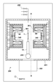
- 2 and 3 are diagrams showing a configuration of one film forming apparatus, and each of the chambers 117 to 130 (excluding 112 to 114) corresponds to the chamber 201 of FIG.
- FIG. 2 is a cross-sectional view of the film forming apparatus 200 taken along a plane (plane along the transport direction) orthogonal to the transport direction of the carrier 10 (substrate 1).
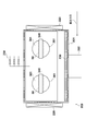
- FIG. 3 is a cross-sectional view taken along line A-A ′ of FIG.
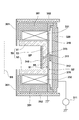
- FIG. 4 shows the configuration of the peripheral portion of the target (sputtering target) 50.
- the film forming apparatus 200 is configured as a sputtering apparatus.
- the film forming apparatus (sputtering apparatus) 200 includes a chamber 201, a transport apparatus 230 that transports the carrier 10, and gate valves 220 disposed on the upstream side and the downstream side of the transport path of the carrier 10 by the transport apparatus 230.
- the chamber 201 is connected to an adjacent chamber through a gate valve 220.
- the film forming apparatus 200 includes a gas supply unit 290 and an exhaust device 202. Gas is supplied to the chamber 201 by the gas supply unit 290, and the gas in the chamber 201 is exhausted by the exhaust device 202, whereby the pressure in the chamber 201 is controlled to the target pressure.
- films are simultaneously formed on the two surfaces of the two substrates 1 by sputtering.
- Four targets 50 are disposed in the chamber 201. Specifically, the first target 50 opposes one surface of the first substrate, the second target 50 opposes the other surface of the first substrate, and the one surface of the second substrate. The third target 50 faces and the fourth target 50 faces the other surface of the second substrate.
- the film forming apparatus 200 may be configured such that a film is formed only on one substrate 1 at a time in one chamber 201.
- the film forming apparatus 200 includes an electrode (cathode) 310 as a backing plate, a first magnet 331, a second magnet 332, and a shield 340.
- the electrode 310 includes a holding unit 311 that holds the target 50, and is configured to apply a potential to the target 50 via the holding unit 311.
- a potential can be applied to the electrode 310 from a power source 371 via the base member 320.
- the power source 371 can be, for example, a pulse DC power source, but may be another power source.
- the first magnet 331 and the second magnet 332 can be composed of permanent magnets, for example.
- the first magnet 331 and the second magnet 332 are spaced apart from each other in a direction along the substrate placement surface SS so as to sandwich the space SP between the substrate placement surface SS where the substrate 1 is to be placed and the holding unit 311.
- the shield 340 is arranged at a position between the first magnet 331 and the second magnet 332 and between the substrate arrangement surface SS and the holding unit 311.
- the target 50 includes a first portion 51 to be disposed between the first magnet 331 and the space SP, a second magnet 332, and the space SP. 2nd part 52 which should be arrange
- the connecting portion 53 is fixed to the holding portion 311.
- the holding part 311 has an engaging part 312 with which a fixing member 315 for fixing the target 50 is engaged.
- the engaging portion 312 is a screw hole
- the fixing member 315 is a screw.
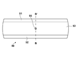
- the fixing member 315 passes through the hole 55 provided in the connecting portion 53 of the target 50 and is screwed into the engaging portion 312. A potential is applied to the first portion 51 and the second portion 52 from the electrode 310 via the connecting portion 53.
- the structure in which the target 50 is supported by the holding portion 311 of the electrode 310 holding the connecting portion 53 among the first portion 51, the second portion 52, and the connecting portion 53 of the target 50 is that the target 50 is mounted on the electrode 310. And it is advantageous for facilitating the work of removing the target 50 from the electrode 310.
- FIG. 5A and 5B show one configuration example of the target 50.
- FIG. The first portion 51 and the second portion 52 of the target 50 can be parallel to each other, as illustrated in FIGS. 5A and 5B.
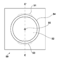
- 6A and 6B show other configuration examples of the target 50.
- FIG. The first portion 51 and the second portion 52 of the target 50 may be portions facing each other in the cylindrical portion 54 as illustrated in FIGS. 6A and 6B.
- first portion 51, the second portion 52, and the connecting portion 53 are integrally formed of the same material.
- first portion 51 and the second portion 52 may be made of the same material (target material, for example, carbon), and the connecting portion 53 may be made of a material different from the material of the first portion 51 and the second portion 52. .
- target material for example, carbon
- the connecting portion 53 should be formed of a superior material.
- first portion 51 and the second portion 52 may be made of different materials.
- a film made of different materials is formed on the substrate 1, that is, simultaneous sputtering is realized.
- the shield 340 can be supplied with a potential that can prevent the connection portion 53 of the target 50 from being sputtered, for example, an installation potential.
- the shield 340 is disposed away from the connecting portion 53 so as not to short-circuit with the connecting portion 53.
- the holding unit 311 has a first surface S1 for holding the target and a second surface S2 opposite to the first surface S1, and the film forming apparatus 200 is on the second surface S2 side of the holding unit 311.
- a cooling channel 370 for cooling the electrode 310 may be provided.
- the cooling channel 370 may be formed between the electrode 310 (holding unit 311) and the base member 320.
- the first portion 51 and the second portion 52 of the target 50 are cooled by cooling the connection portion 53 of the target 50 via the holding unit 311 by the cooling medium flowing through the cooling channel 370.
- the cooling medium Between the first magnet 331 and the position where the first portion 51 of the target 50 is to be disposed, and between the second magnet 332 and the position where the second portion 52 of the target 50 is to be disposed, the cooling medium. It is preferable that no cooling channel is provided for flowing the water. Cooling channels are disposed between the first magnet 331 and the position where the first portion 51 of the target 50 is to be disposed, and between the second magnet 332 and the position where the second portion 52 of the target 50 is to be disposed. By not, the magnetic field generated by the first magnet 331 and the second magnet 332 can be guided to the space SP with little attenuation. This is advantageous in reducing the size of the first magnet 331 and the second magnet 332.
- the film forming apparatus 200 further includes a second shield 361 between the position where the first magnet 331 and the second magnet 332 are disposed and the substrate arrangement surface SS.
- a block 351 may be disposed outside the first magnet 331 and the second magnet 332.
- the block 351 can be made of aluminum, for example.
- a third shield 352 may be disposed outside the block 351 so as to surround the block 351, the electrode 310, and the base member 320.
- the third shield 352 can be electrically connected to the second shield 361.
- the second shield 361 and the third shield 352 can be grounded.
- the exhaust device 202 While supplying the gas from the gas supply unit 290 to the chamber 201, the exhaust device 202 exhausts the gas in the chamber 201 to control the pressure in the chamber 201 to the target pressure, while the target is supplied from the power source 371 through the electrode 310.
- a potential to the 50 first portion 51 and the second portion 52 By applying a potential to the 50 first portion 51 and the second portion 52, a discharge occurs in the space SP.
- the first portion 51 and the second portion 52 of the target 50 are sputtered by the ions generated thereby. Thereby, a film is formed on the substrate 1 by the particles flying from the first portion 51 and the second portion 52 of the target 50.
Landscapes
- Chemical & Material Sciences (AREA)
- Engineering & Computer Science (AREA)
- Physics & Mathematics (AREA)
- Plasma & Fusion (AREA)
- Analytical Chemistry (AREA)
- Chemical Kinetics & Catalysis (AREA)
- Materials Engineering (AREA)
- Mechanical Engineering (AREA)
- Metallurgy (AREA)
- Organic Chemistry (AREA)
- Physical Vapour Deposition (AREA)
- Manufacturing Of Magnetic Record Carriers (AREA)
Abstract
スパッタリング装置は、ターゲット50を保持する保持部311を有し保持部311を介してターゲット50に電位を与える電極310と、基板が配置されるべき基板配置面SSと保持部311との間の空間SPを挟むように、かつ、基板配置面SSに沿った方向に互いに離隔して配置された第1マグネット331および第2マグネット332と、第1マグネット331と第2マグネット332との間かつ基板配置面SSと保持部311との間の位置に配置されるシールド340と、を備える。
Description
本発明は、スパッタリング装置およびスパッタリング用ターゲットに関する。
特許文献1には、処理対象の基板の1つの面が対面する空間を挟むように対向して配置された一対のターゲットを備える箱型対向ターゲット式スパッタ装置が記載されている。各ターゲットの背面側には永久磁石が配置され、ターゲットと永久磁石との間には冷却ジャケットが配置されている。各ターゲットは、冷却ジャケットを構成する部分や永久磁石などとともに組み上げられてターゲット部を構成している。各ターゲット部は、それぞれ枠体に固定される。
特許文献1に記載された箱型対向ターゲット式スパッタ装置では、一対のターゲット部のそれぞれを枠体に取り付ける必要がある。しかも、各ターゲット部は、ターゲットの他に冷却ジャケットを構成する部分や永久磁石などを含むので大型である。したがって、特許文献1に記載された箱型対向ターゲット式スパッタ装置では、ターゲットの交換などのメンテナンスにかなりに時間を要すると考えられる。また、永久磁石とターゲットとの間に冷却ジャケットを配置した構成では、永久磁石が発生する磁界が冷却ジャケット中の冷媒などによって減衰するので永久磁石を大型化する必要がある。
本発明は、新規且つ有用な構造を有するスパッタリング装置およびスパッタリング用ターゲットを提供することを目的とする。
本発明の1つの側面は、チャンバの中でスパッタリングによって基板に膜を形成するスパッタリング装置に係り、前記スパッタリング装置は、ターゲットを保持する保持部を有し前記保持部を介して前記ターゲットに電位を与える電極と、基板が配置されるべき基板配置面と前記保持部との間の空間を挟むように、かつ、前記基板配置面に沿った方向に互いに離隔して配置された第1マグネットおよび第2マグネットと、前記第1マグネットと前記第2マグネットとの間かつ前記基板配置面と前記保持部との間の位置に配置されるシールドと、を備える。
本発明の他の側面は、スパッタリング用ターゲットに係り、前記スパッタリング用ターゲットは、互いに対向する第1部分および第2部分と、前記第1部分と前記第2部分とを連結する連結部分とを含み、前記連結部分に電位が与えられることによって前記第1部分および前記第2部分に電位が与えられる。
本発明によれば、新規且つ有用な構造を有するスパッタリング装置およびスパッタリング用ターゲットが提供される。
以下、添付図面を参照しながら本発明をその例示的な実施形態を通して説明する。
図1は、本発明の1つの実施形態の処理システム100の構成を概略的に示す平面図である。処理システム100は、インライン式の処理装置として構成されている。インライン式とは、連結された複数のチャンバを経由して基板を搬送しながら基板を処理する方式をいう。図1に示す成膜装置200では、複数のチャンバ111~130が方形のレイアウトを構成するように無端状に連結されている。チャンバ111~130の各々には、キャリア10によって保持された基板1を搬送する搬送装置が備えられている。チャンバ111~130における互いに隣接するチャンバは、ゲートバルブを介して連結されている。チャンバ111は、キャリア10に基板1を取り付ける処理が行われるロードロック室である。チャンバ116は、キャリア10から基板1を取り外す処理が行われるアンロードロック室である。
より具体的な例を提示するために、処理システム100がハードディスクを製造するための処理装置に適用された例を説明する。基板1は、例えば、中心部分に孔を有する金属製若しくはガラス製の円板状部材でありうる。キャリア10は、2枚の基板を保持するように構成されうる。
まず、チャンバ111内で未処理の2枚の基板1が先頭のキャリア10に取り付けられる。キャリア10は、密着層を形成するためのチャンバ117に移動して、基板1に密着層が形成される。この間に、2番目のキャリア10に対して2枚の未処理の基板1が取り付けられる。
次いで、先頭のキャリア10が軟磁性層を形成するためのチャンバ118、119、120に順に移動しながら基板1に軟磁性層が形成される。この間、2番目のキャリア10が密着層を形成するためのチャンバ117に移動し、基板1に密着層が形成され、更に、チャンバ111内では、3番目のキャリア10に対して基板1が取り付けられる。このようにして、先頭のキャリア10およびそれに続くキャリア10が移動する度に、チャンバ111内において後続のキャリア10に対して基板1が取り付けられる。
軟磁性層が形成された基板1を保持している先頭のキャリア10は、シード層を形成するためのチャンバ121に移動し、基板1にシード層が形成される。その後、先頭のキャリア10は、中間層を形成するためのチャンバ123、124、磁性膜を形成するためのチャンバ126、127、保護膜を形成するためのチャンバ129に順に移動する。
方形のレイアウトにおける四隅の部分には、チャンバ112、113、114、115が配置されている。チャンバ112、113、114、115は、キャリア10(基板1)の搬送方向を90度転換する方向転換装置を備えたチャンバである。
チャンバ117~130(112~114を除く)は、それぞれ成膜装置の構成要素である。図2および図3は、1つの成膜装置の構成を示す図であり、チャンバ117~130(112~114を除く)の各々は、図2のチャンバ201に対応する。図2は、成膜装置200をキャリア10(基板1)の搬送方向に直交する面(搬送方向に沿った面)で切断した断面図である。図3には、図2のA-A’線に沿った断面図が示されている。図4には、ターゲット(スパッタリング用ターゲット)50の周辺部分の構成が示されている。成膜装置200は、スパッタリング装置として構成されている。
成膜装置(スパッタリング装置)200は、チャンバ201と、キャリア10を搬送する搬送装置230と、搬送装置230によるキャリア10の搬送経路の上流側および下流側に配置されたゲートバルブ220を有する。チャンバ201は、ゲートバルブ220を介して隣接するチャンバと接続されている。
成膜装置200は、ガス供給部290および排気装置202を備える。チャンバ201には、ガス供給部290によってガスが供給され、チャンバ201内のガスは、排気装置202により排気され、これによってチャンバ201内の圧力が目標圧力に制御される。
この実施形態では、チャンバ201の中では、2枚の基板1のそれぞれの2つの面に対して、同時に、スパッタリングによって膜が形成される。チャンバ201の中には、4つのターゲット50が配置されている。具体的には、第1の基板の1つの面に第1のターゲット50が対向し、第1の基板の他の面に第2のターゲット50が対向し、第2の基板の1つの面に第3のターゲット50が対向し、第2の基板の他の面に第4のターゲット50が対向する。なお、成膜装置200は、1つのチャンバ201の中で一度に1枚の基板1にのみ膜が形成されるように構成されてもよい。
図4に例示されるように、成膜装置200は、バッキングプレートとしての電極(カソード)310と、第1マグネット331と、第2マグネット332と、シールド340とを備えている。電極310は、ターゲット50を保持する保持部311を有し、保持部311を介してターゲット50に電位を与えるように構成されている。電極310には、例えば、ベース部材320を介して電源371から電位が与えられうる。電源371は、例えば、パルスDC電源でありうるが、他の電源であってもよい。
第1マグネット331および第2マグネット332は、例えば永久磁石で構成されうる。第1マグネット331および第2マグネット332は、基板1が配置されるべき基板配置面SSと保持部311との間の空間SPを挟むように、かつ、基板配置面SSに沿った方向に互いに離隔して配置されている。シールド340は、第1マグネット331と第2マグネット332との間かつ基板配置面SSと保持部311との間の位置に配置されている。
ターゲット50は、図5A、5B、6A、6Bに例示的に示されるように、第1マグネット331と空間SPとの間に配置されるべき第1部分51と、第2マグネット332と空間SPとの間に配置されるべき第2部分52と、第1部分51と第2部分52とを連結する連結部分53とを含む。ターゲット50は、連結部分53が保持部311に固定される。保持部311は、ターゲット50を固定するための固定部材315が係合される係合部312を有する。一例において、係合部312は、ねじ穴であり、固定部材315は、ねじである。固定部材315は、ターゲット50の連結部分53に設けられた穴55を貫通して係合部312に捩じ込まれる。第1部分51および第2部分52には、電極310から連結部分53を介して電位が与えられる。
電極310の保持部311がターゲット50の第1部分51、第2部分52および連結部分53のうち連結部分53を保持することによってターゲット50が支持される構造は、電極310へのターゲット50の装着および電極310からのターゲット50の取り外しの作業の容易化に有利である。
図5A、5Bには、ターゲット50の1つの構成例が示されている。ターゲット50の第1部分51および第2部分52は、図5A、5Bに例示されるように、互いに平行でありうる。図6A、6Bには、ターゲット50の他の構成例が示されている。ターゲット50の第1部分51および第2部分52は、図6A、6Bに例示されるように、円筒部54における互いに対向する部分でありうる。
第1部分51、第2部分52および連結部分53は、同一材料で一体的に構成されることが好ましい。しかしながら、第1部分51および第2部分52を同一材料(ターゲット材料、例えば炭素)で構成し、連結部分53を第1部分51および第2部分52の材料とは異なる材料で構成してもよい。この場合は、第1部分51および第2部分52の効率的な冷却、並びに、第1部分51および第2部分52への効率的な電位の供給のために、電気伝導性および熱伝導性に優れた材料で連結部分53を形成するべきである。
更に、第1部分51と第2部分52とを互いに異なる材料で構成してもよく、この場合、互いに異なる材料からなる膜を基板1の上に形成すること、即ち同時スパッタリングが実現される。
シールド340には、ターゲット50の連結部分53がスパッタリングされることを防止することができる電位、例えば設置電位が与えられうる。シールド340は、連結部分53と短絡しないように、連結部分53から離隔して配置される。
保持部311は、ターゲットを保持するための第1面S1と、第1面S1の反対側の第2面S2とを有し、成膜装置200は、保持部311の第2面S2の側に、電極310を冷却するための冷却チャネル370を備えうる。冷却チャネル370は、電極310(保持部311)とベース部材320との間に形成されうる。ターゲット50の第1部分51および第2部分52は、冷却チャネル370を流れる冷却媒体によって保持部311を介してターゲット50の連結部分53が冷却されることによって冷却される。
第1マグネット331とターゲット50の第1部分51が配置されるべき位置との間、および、第2マグネット332とターゲット50の第2部分52が配置されるべき位置との間には、冷却媒体を流すための冷却チャネルが設けられていないことが好ましい。第1マグネット331とターゲット50の第1部分51が配置されるべき位置との間、および、第2マグネット332とターゲット50の第2部分52が配置されるべき位置との間に冷却チャネルを配置しないことによって、第1マグネット331および第2マグネット332が発生する磁界を少ない減衰で空間SPに導くことができる。これは、第1マグネット331および第2マグネット332の小型化に有利である。
成膜装置200は、更に、第1マグネット331および第2マグネット332が配置された位置と基板配置面SSとの間に第2シールド361を備えることが好ましい。第1マグネット331および第2マグネット332の外側には、ブロック351が配置されうる。ブロック351は、例えば、アルミニウムで構成されうる。ブロック351の外側には、ブロック351、電極310およびベース部材320を取り囲むように第3シールド352が配置されうる。第3シールド352は、第2シールド361と電気的に接続されうる。第2シールド361および第3シールド352は、接地されうる。
ガス供給部290からチャンバ201内にガスを供給しつつ排気装置202によってチャンバ201内のガスを排気することによってチャンバ201内の圧力を目標圧力に制御しながら、電源371から電極310を介してターゲット50の第1部分51および第2部分52に電位を与えることによって空間SPにおいて放電が生じる。これによって発生したイオンによってターゲット50の第1部分51および第2部分52がスパッタリングされる。これにより、ターゲット50の第1部分51および第2部分52から飛びした粒子によって基板1の上に膜が形成される。
本発明は上記実施の形態に制限されるものではなく、本発明の精神及び範囲から離脱することなく、様々な変更及び変形が可能である。従って、本発明の範囲を公にするために、以下の請求項を添付する。
本願は、2013年8月2日提出の日本国特許出願特願2013-161847を基礎として優先権を主張するものであり、その記載内容の全てを、ここに援用する。
Claims (12)
- チャンバの中でスパッタリングによって基板に膜を形成するスパッタリング装置であって、
ターゲットを保持する保持部を有し前記保持部を介して前記ターゲットに電位を与える電極と、
基板が配置されるべき基板配置面と前記保持部との間の空間を挟むように、かつ、前記基板配置面に沿った方向に互いに離隔して配置された第1マグネットおよび第2マグネットと、
前記第1マグネットと前記第2マグネットとの間かつ前記基板配置面と前記保持部との間の位置に配置されるシールドと、
を備えることを特徴とするスパッタリング装置。 - 前記ターゲットは、前記第1マグネットと前記空間との間に配置されるべき第1部分と、前記第2マグネットと前記空間との間に配置されるべき第2部分と、前記第1部分と前記第2部分とを連結する連結部分とを含み、
前記連結部分が前記保持部に固定される、
ことを特徴とする請求項1に記載のスパッタリング装置。 - 前記保持部は、前記ターゲットを保持するための第1面と、前記第1面の反対側の第2面とを有し、
前記スパッタリング装置は、前記保持部の前記第2面の側に、前記電極を冷却するための冷却チャネルを備え、
前記ターゲットの前記第1部分および前記第2部分は、前記冷却チャネルを流れる冷却媒体によって前記保持部を介して前記連結部分が冷却されることによって冷却される、
ことを特徴とする請求項2に記載のスパッタリング装置。 - 前記第1マグネットと前記ターゲットの前記第1部分が配置されるべき位置との間および前記第2マグネットと前記ターゲットの前記第2部分が配置されるべき位置との間には、冷却媒体を流すための冷却チャネルが設けられていない、
ことを特徴とする請求項2又は3に記載のスパッタリング装置。 - 前記保持部は、前記ターゲットを固定するための固定部材が係合される係合部を有する、
ことを特徴とする請求項1乃至4のいずれか1項に記載のスパッタリング装置。 - 前記係合部は、ねじ穴である、
ことを特徴とする請求項5に記載のスパッタリング装置。 - 前記第1マグネットおよび前記第2マグネットが配置された位置と前記基板配置面との間に第2シールドを備える、
ことを特徴とする請求項1乃至6のいずれか1項に記載のスパッタリング装置。 - 互いに対向する第1部分および第2部分と、前記第1部分と前記第2部分とを連結する連結部分とを含み、前記連結部分に電位が与えられることによって前記第1部分および前記第2部分に電位が与えられることを特徴とするスパッタリング用ターゲット。
- 前記連結部分に、前記スパッタリング用ターゲットを電極に固定するための穴が設けられている、
ことを特徴とする請求項8に記載のスパッタリング用ターゲット。 - 前記第1部分と前記第2部分とは互いに平行である、
ことを特徴とする請求項8又は9に記載のスパッタリング用ターゲット。 - 前記第1部分および前記第2部分は、円筒部における互いに対向する部分である、
ことを特徴とする請求項8又は9に記載のスパッタリング用ターゲット。 - 前記第1部分、前記第2部分および前記連結部分が同一材料で一体的に形成されている、
ことを特徴とする請求項8乃至11のいずれか1項に記載のスパッタリング用ターゲット。
Applications Claiming Priority (2)
| Application Number | Priority Date | Filing Date | Title |
|---|---|---|---|
| JP2013-161847 | 2013-08-02 | ||
| JP2013161847 | 2013-08-02 |
Publications (1)
| Publication Number | Publication Date |
|---|---|
| WO2015015669A1 true WO2015015669A1 (ja) | 2015-02-05 |
Family
ID=52431235
Family Applications (2)
| Application Number | Title | Priority Date | Filing Date |
|---|---|---|---|
| PCT/JP2014/000672 Ceased WO2015015669A1 (ja) | 2013-08-02 | 2014-02-07 | スパッタリング装置およびスパッタリング用ターゲット |
| PCT/JP2014/003909 Ceased WO2015015775A1 (ja) | 2013-08-02 | 2014-07-24 | スパッタリング装置およびスパッタリング用ターゲット |
Family Applications After (1)
| Application Number | Title | Priority Date | Filing Date |
|---|---|---|---|
| PCT/JP2014/003909 Ceased WO2015015775A1 (ja) | 2013-08-02 | 2014-07-24 | スパッタリング装置およびスパッタリング用ターゲット |
Country Status (3)
| Country | Link |
|---|---|
| JP (1) | JP2015045087A (ja) |
| TW (1) | TW201522686A (ja) |
| WO (2) | WO2015015669A1 (ja) |
Families Citing this family (1)
| Publication number | Priority date | Publication date | Assignee | Title |
|---|---|---|---|---|
| DE102016125273A1 (de) | 2016-12-14 | 2018-06-14 | Schneider Gmbh & Co. Kg | Anlage, Verfahren und Träger zur Beschichtung von Brillengläsern |
Citations (4)
| Publication number | Priority date | Publication date | Assignee | Title |
|---|---|---|---|---|
| JPS60234970A (ja) * | 1984-04-19 | 1985-11-21 | バルツエルス・アクチエンゲゼルシヤフト | カソードスパツタによる基板被覆装置 |
| JPS61201773A (ja) * | 1985-03-04 | 1986-09-06 | Showa Denko Kk | スパツタリング方法及びその装置 |
| JPH05222524A (ja) * | 1992-02-07 | 1993-08-31 | Toshiba Corp | スパッタ装置 |
| JPH09235668A (ja) * | 1996-02-23 | 1997-09-09 | Balzers Prozes Syst Gmbh | 中空ターゲットを用いて陰極スパッタリングによって基板を被覆するための装置 |
Family Cites Families (6)
| Publication number | Priority date | Publication date | Assignee | Title |
|---|---|---|---|---|
| JPS59220912A (ja) * | 1983-05-31 | 1984-12-12 | Fujitsu Ltd | スパツタリング装置 |
| JPH05182911A (ja) * | 1991-12-27 | 1993-07-23 | Hitachi Ltd | スパッタ装置 |
| JPH09228038A (ja) * | 1996-02-23 | 1997-09-02 | Balzers Prozes Syst Gmbh | 中空のターゲットを備えた、陰極スパッタによりサブストレートを被覆するための装置 |
| JP2006169610A (ja) * | 2004-12-20 | 2006-06-29 | Matsushita Electric Ind Co Ltd | スパッタリング装置 |
| JP2007291477A (ja) * | 2006-04-27 | 2007-11-08 | Matsushita Electric Ind Co Ltd | スパッタリング装置 |
| JP2011063823A (ja) * | 2009-09-15 | 2011-03-31 | Promatic Kk | スパッタ源およびスパッタ装置ならびにこれを用いた多層膜の製造方法 |
-
2014
- 2014-02-07 WO PCT/JP2014/000672 patent/WO2015015669A1/ja not_active Ceased
- 2014-07-24 JP JP2014151007A patent/JP2015045087A/ja active Pending
- 2014-07-24 WO PCT/JP2014/003909 patent/WO2015015775A1/ja not_active Ceased
- 2014-08-01 TW TW103126399A patent/TW201522686A/zh unknown
Patent Citations (4)
| Publication number | Priority date | Publication date | Assignee | Title |
|---|---|---|---|---|
| JPS60234970A (ja) * | 1984-04-19 | 1985-11-21 | バルツエルス・アクチエンゲゼルシヤフト | カソードスパツタによる基板被覆装置 |
| JPS61201773A (ja) * | 1985-03-04 | 1986-09-06 | Showa Denko Kk | スパツタリング方法及びその装置 |
| JPH05222524A (ja) * | 1992-02-07 | 1993-08-31 | Toshiba Corp | スパッタ装置 |
| JPH09235668A (ja) * | 1996-02-23 | 1997-09-09 | Balzers Prozes Syst Gmbh | 中空ターゲットを用いて陰極スパッタリングによって基板を被覆するための装置 |
Also Published As
| Publication number | Publication date |
|---|---|
| TW201522686A (zh) | 2015-06-16 |
| JP2015045087A (ja) | 2015-03-12 |
| WO2015015775A1 (ja) | 2015-02-05 |
Similar Documents
| Publication | Publication Date | Title |
|---|---|---|
| JP5454976B2 (ja) | 薄膜形成方法及び薄膜形成装置 | |
| JP5004931B2 (ja) | スパッタ源、スパッタリング装置、及びスパッタリング方法 | |
| KR101473949B1 (ko) | 스퍼터링 장치 및 스퍼터링 방법 | |
| KR20190087382A (ko) | 성막 시스템, 자성체부 및 막의 제조 방법 | |
| WO2014119580A1 (ja) | 薄型基板処理装置 | |
| JP6416261B2 (ja) | 基板処理装置及び基板処理方法 | |
| JP2004346356A (ja) | マスクユニットおよびそれを用いた成膜装置 | |
| WO2015015669A1 (ja) | スパッタリング装置およびスパッタリング用ターゲット | |
| US20100006429A1 (en) | Sputtering apparatus and manufacturing apparatus for liquid crystal device | |
| JP2016141825A (ja) | スパッタリング装置 | |
| JP7759767B2 (ja) | マグネトロンスパッタリング装置及びスパッタリング方法 | |
| US20160027624A1 (en) | Sputtering apparatus | |
| TW202025413A (zh) | 於真空腔室中用以冷卻沉積區域的冷卻系統,用於在基板上進行材料沉積的裝置,以及在沉積區域中的基板上進行材料沉積的方法 | |
| KR101515048B1 (ko) | 캐소드 | |
| JP2023084397A (ja) | 成膜方法及び成膜装置 | |
| JPH03243761A (ja) | スパッタリング装置 | |
| JP2017115215A (ja) | 有機el表示装置の製造装置 | |
| JP5781408B2 (ja) | マグネトロンスパッタカソード | |
| JP5467894B2 (ja) | 基板処理装置及び表示用素子の製造方法 | |
| KR20250117420A (ko) | 기판 보유지지 장치 및 성막 장치 | |
| KR20250117818A (ko) | 기판 보유지지 장치, 성막 장치, 및 성막 장치의 제어 방법 | |
| WO2024128132A1 (ja) | 成膜装置 | |
| WO2012140798A1 (ja) | ターゲット及びターゲットの製造方法 | |
| JP5072700B2 (ja) | 成膜装置 | |
| JP2013197401A (ja) | ロードロックチャンバ |
Legal Events
| Date | Code | Title | Description |
|---|---|---|---|
| 121 | Ep: the epo has been informed by wipo that ep was designated in this application |
Ref document number: 14832503 Country of ref document: EP Kind code of ref document: A1 |
|
| NENP | Non-entry into the national phase |
Ref country code: DE |
|
| 122 | Ep: pct application non-entry in european phase |
Ref document number: 14832503 Country of ref document: EP Kind code of ref document: A1 |
|
| NENP | Non-entry into the national phase |
Ref country code: JP |