WO2014203904A1 - 炭化珪素半導体装置の製造方法 - Google Patents
炭化珪素半導体装置の製造方法 Download PDFInfo
- Publication number
- WO2014203904A1 WO2014203904A1 PCT/JP2014/066053 JP2014066053W WO2014203904A1 WO 2014203904 A1 WO2014203904 A1 WO 2014203904A1 JP 2014066053 W JP2014066053 W JP 2014066053W WO 2014203904 A1 WO2014203904 A1 WO 2014203904A1
- Authority
- WO
- WIPO (PCT)
- Prior art keywords
- silicon carbide
- heat treatment
- insulating film
- semiconductor device
- manufacturing
- Prior art date
- Legal status (The legal status is an assumption and is not a legal conclusion. Google has not performed a legal analysis and makes no representation as to the accuracy of the status listed.)
- Ceased
Links
Images






Classifications
-
- H—ELECTRICITY
- H10—SEMICONDUCTOR DEVICES; ELECTRIC SOLID-STATE DEVICES NOT OTHERWISE PROVIDED FOR
- H10D—INORGANIC ELECTRIC SEMICONDUCTOR DEVICES
- H10D64/00—Electrodes of devices having potential barriers
- H10D64/01—Manufacture or treatment
- H10D64/013—Manufacture or treatment of electrodes having a conductor capacitively coupled to a semiconductor by an insulator
- H10D64/01366—Manufacture or treatment of electrodes having a conductor capacitively coupled to a semiconductor by an insulator the semiconductor being silicon carbide
-
- H—ELECTRICITY
- H10—SEMICONDUCTOR DEVICES; ELECTRIC SOLID-STATE DEVICES NOT OTHERWISE PROVIDED FOR
- H10D—INORGANIC ELECTRIC SEMICONDUCTOR DEVICES
- H10D12/00—Bipolar devices controlled by the field effect, e.g. insulated-gate bipolar transistors [IGBT]
- H10D12/01—Manufacture or treatment
- H10D12/031—Manufacture or treatment of IGBTs
-
- H—ELECTRICITY
- H10—SEMICONDUCTOR DEVICES; ELECTRIC SOLID-STATE DEVICES NOT OTHERWISE PROVIDED FOR
- H10D—INORGANIC ELECTRIC SEMICONDUCTOR DEVICES
- H10D30/00—Field-effect transistors [FET]
- H10D30/01—Manufacture or treatment
- H10D30/021—Manufacture or treatment of FETs having insulated gates [IGFET]
- H10D30/028—Manufacture or treatment of FETs having insulated gates [IGFET] of double-diffused metal oxide semiconductor [DMOS] FETs
- H10D30/0291—Manufacture or treatment of FETs having insulated gates [IGFET] of double-diffused metal oxide semiconductor [DMOS] FETs of vertical DMOS [VDMOS] FETs
-
- H—ELECTRICITY
- H10—SEMICONDUCTOR DEVICES; ELECTRIC SOLID-STATE DEVICES NOT OTHERWISE PROVIDED FOR
- H10D—INORGANIC ELECTRIC SEMICONDUCTOR DEVICES
- H10D30/00—Field-effect transistors [FET]
- H10D30/60—Insulated-gate field-effect transistors [IGFET]
-
- H—ELECTRICITY
- H10—SEMICONDUCTOR DEVICES; ELECTRIC SOLID-STATE DEVICES NOT OTHERWISE PROVIDED FOR
- H10D—INORGANIC ELECTRIC SEMICONDUCTOR DEVICES
- H10D30/00—Field-effect transistors [FET]
- H10D30/60—Insulated-gate field-effect transistors [IGFET]
- H10D30/64—Double-diffused metal-oxide semiconductor [DMOS] FETs
- H10D30/66—Vertical DMOS [VDMOS] FETs
-
- H—ELECTRICITY
- H10—SEMICONDUCTOR DEVICES; ELECTRIC SOLID-STATE DEVICES NOT OTHERWISE PROVIDED FOR
- H10D—INORGANIC ELECTRIC SEMICONDUCTOR DEVICES
- H10D30/00—Field-effect transistors [FET]
- H10D30/60—Insulated-gate field-effect transistors [IGFET]
- H10D30/64—Double-diffused metal-oxide semiconductor [DMOS] FETs
- H10D30/66—Vertical DMOS [VDMOS] FETs
- H10D30/662—Vertical DMOS [VDMOS] FETs having a drift region having a doping concentration that is higher between adjacent body regions relative to other parts of the drift region
-
- H—ELECTRICITY
- H10—SEMICONDUCTOR DEVICES; ELECTRIC SOLID-STATE DEVICES NOT OTHERWISE PROVIDED FOR
- H10D—INORGANIC ELECTRIC SEMICONDUCTOR DEVICES
- H10D62/00—Semiconductor bodies, or regions thereof, of devices having potential barriers
- H10D62/10—Shapes, relative sizes or dispositions of the regions of the semiconductor bodies; Shapes of the semiconductor bodies
- H10D62/13—Semiconductor regions connected to electrodes carrying current to be rectified, amplified or switched, e.g. source or drain regions
- H10D62/149—Source or drain regions of field-effect devices
- H10D62/151—Source or drain regions of field-effect devices of IGFETs
- H10D62/156—Drain regions of DMOS transistors
- H10D62/157—Impurity concentrations or distributions
-
- H—ELECTRICITY
- H10—SEMICONDUCTOR DEVICES; ELECTRIC SOLID-STATE DEVICES NOT OTHERWISE PROVIDED FOR
- H10D—INORGANIC ELECTRIC SEMICONDUCTOR DEVICES
- H10D62/00—Semiconductor bodies, or regions thereof, of devices having potential barriers
- H10D62/10—Shapes, relative sizes or dispositions of the regions of the semiconductor bodies; Shapes of the semiconductor bodies
- H10D62/17—Semiconductor regions connected to electrodes not carrying current to be rectified, amplified or switched, e.g. channel regions
- H10D62/393—Body regions of DMOS transistors or IGBTs
-
- H—ELECTRICITY
- H10—SEMICONDUCTOR DEVICES; ELECTRIC SOLID-STATE DEVICES NOT OTHERWISE PROVIDED FOR
- H10D—INORGANIC ELECTRIC SEMICONDUCTOR DEVICES
- H10D62/00—Semiconductor bodies, or regions thereof, of devices having potential barriers
- H10D62/40—Crystalline structures
- H10D62/405—Orientations of crystalline planes
-
- H—ELECTRICITY
- H10—SEMICONDUCTOR DEVICES; ELECTRIC SOLID-STATE DEVICES NOT OTHERWISE PROVIDED FOR
- H10D—INORGANIC ELECTRIC SEMICONDUCTOR DEVICES
- H10D62/00—Semiconductor bodies, or regions thereof, of devices having potential barriers
- H10D62/80—Semiconductor bodies, or regions thereof, of devices having potential barriers characterised by the materials
- H10D62/83—Semiconductor bodies, or regions thereof, of devices having potential barriers characterised by the materials being Group IV materials, e.g. B-doped Si or undoped Ge
- H10D62/832—Semiconductor bodies, or regions thereof, of devices having potential barriers characterised by the materials being Group IV materials, e.g. B-doped Si or undoped Ge being Group IV materials comprising two or more elements, e.g. SiGe
- H10D62/8325—Silicon carbide
-
- H—ELECTRICITY
- H10—SEMICONDUCTOR DEVICES; ELECTRIC SOLID-STATE DEVICES NOT OTHERWISE PROVIDED FOR
- H10D—INORGANIC ELECTRIC SEMICONDUCTOR DEVICES
- H10D64/00—Electrodes of devices having potential barriers
- H10D64/01—Manufacture or treatment
- H10D64/013—Manufacture or treatment of electrodes having a conductor capacitively coupled to a semiconductor by an insulator
- H10D64/01364—Manufacture or treatment of electrodes having a conductor capacitively coupled to a semiconductor by an insulator the semiconductor being diamond, semiconducting diamond-like carbon or graphene
Definitions
- the present invention relates to a method of manufacturing a silicon carbide semiconductor device.
- silicon carbide can form a gate insulating film by thermal oxidation.
- MOS gate metal-oxide film-semiconductor insulated gate
- MOS gate interface silicon carbide substrate
- the interface state density is an index to evaluate the channel mobility alternatively. In general, it is known that the lower the interface state density at the MOS gate interface, the higher the channel mobility.
- a method of performing thermal oxidation using an atmosphere containing nitrogen such as nitrous oxide (N 2 O) or nitrogen monoxide (NO) is known.
- nitrogen atoms contained in the atmosphere contribute to termination of dangling bonds of silicon atoms in the gate insulating film or at the MOS gate interface, and at the MOS gate interface It is said that the effect is to reduce the interface state density of
- annealing heat treatment
- H 2 hydrogen
- dangling bonds of silicon atoms remaining after oxidation are terminated by hydrogen atoms, and interface state density at the MOS gate interface is further reduced.
- a heat treatment step such as heat treatment for forming the contact metal and forming a reaction layer (electrical contact portion) between the contact metal and the silicon carbide semiconductor (silicon carbide substrate) is essential.
- Interface properties such as interface state density at the bonding interface between the gate oxide film and the silicon carbide substrate are set to satisfy predetermined conditions in the step of forming the gate insulating film, but are changed by heat treatment after forming the gate insulating film.
- a reaction layer between a contact metal and a silicon carbide semiconductor is formed in manufacturing a MOSFET (insulated gate field effect transistor) having a MOS gate on the (000-1) plane of a silicon carbide substrate.
- Heat treatment for reducing the interface state density at the MOS gate interface is suppressed by performing the heat treatment in a mixed gas atmosphere of an inert gas and hydrogen (forming gas (FG) atmosphere) instead of the inert gas atmosphere.
- FG forming gas
- the conditions for heat treatment performed after the formation of the gate insulating film also need to be considered.
- the semiconductor device be in an off state (hereinafter referred to as normally off) when no signal is input to the gate. That is, it is desirable that the threshold voltage of the semiconductor device be a positive value.
- the threshold voltage is expressed by a function having a flat band voltage as an argument, and in order to make the threshold voltage a positive value, it is desirable that the flat band voltage be a positive value.
- the method for forming a gate insulating film described above that is, thermally oxidizing the (000-1) plane or the (11-20) plane of the silicon carbide substrate in a gas atmosphere containing nitrogen such as nitrous oxide or nitric oxide,
- the flat band voltage has a negative value and a signal is input to the gate. In the absence state, the semiconductor device is turned on (normally on).
- An object of the present invention is to provide a method of manufacturing a silicon carbide semiconductor device which exhibits normally-off characteristics and can reduce interface state density in order to solve the problems of the above-described conventional technology.
- the method for manufacturing a silicon carbide semiconductor device has the following features.
- the semiconductor substrate made of silicon carbide is subjected to a first heat treatment in an oxidizing atmosphere containing an oxide compound containing nitrogen, and then subjected to a second heat treatment in an atmosphere containing hydrogen, whereby the (000-1) plane of the semiconductor substrate or (11-20)
- a step of forming a gate insulating film on a surface inclined at an angle of 0 ° or more and 8 ° or less from the surface is performed.
- a third heat treatment performed after the formation of the gate insulating film is performed in an inert gas atmosphere.
- the temperature of the third heat treatment is equal to or lower than the temperature of the first heat treatment.
- the first heat treatment is performed in an atmosphere containing nitrous oxide or nitric oxide.
- the gate insulating film of the semiconductor substrate is formed before the first heat treatment. It is characterized in that the side surface is oxidized in a dry oxygen atmosphere.
- the gate insulating film in the step of forming the gate insulating film, is formed before the first heat treatment. And depositing a thin insulating film.
- the inert gas atmosphere is an atmosphere containing nitrogen, helium or argon.
- the third heat treatment is a step for forming an electrical contact portion between the semiconductor substrate and a metal film in contact with the semiconductor substrate It is performed in the step for reducing the resistance of the gate electrode formed on the gate insulating film, or in the step for baking the interlayer insulating film which electrically insulates the metal film from the gate electrode. It is characterized by
- the (000-1) plane or (11-20) of the silicon carbide semiconductor substrate can be obtained. Even when the gate insulating film is formed by thermal oxidation in a nitrogen-containing atmosphere on the main surface with a surface inclined at 0 ° to 8 ° from the surface, 4 ⁇ 10 11 cm ⁇ without adding a new step.
- a silicon carbide semiconductor device having a low interface state density of 2 eV ⁇ 1 or less and a positive flat band voltage of 1 V or more can be manufactured.
- FIG. 1 is a flowchart showing an outline of a method of manufacturing a semiconductor device according to the first embodiment.
- FIG. 2 is a cross-sectional view showing a state during manufacture of the silicon carbide semiconductor device according to the first embodiment.
- FIG. 3 is a cross-sectional view showing a state during manufacture of the silicon carbide semiconductor device according to the first embodiment.
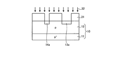
- FIG. 4 is a cross-sectional view showing a state in the middle of manufacturing the silicon carbide semiconductor device according to the first embodiment.
- FIG. 5 is a cross-sectional view showing a state in the middle of manufacturing the silicon carbide semiconductor device according to the first embodiment.
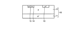
- FIG. 6 is a cross-sectional view showing a state in the middle of manufacturing the silicon carbide semiconductor device according to the first embodiment.
- FIG. 7 is a cross-sectional view showing a state in the middle of manufacturing the silicon carbide semiconductor device according to the first embodiment.
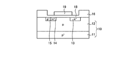
- FIG. 8 is a cross-sectional view showing a state in the middle of manufacturing the silicon carbide semiconductor device according to the first embodiment.
- FIG. 9 is a cross-sectional view showing a state in the middle of manufacturing the silicon carbide semiconductor device according to the first embodiment.
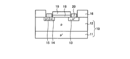
- FIG. 10 is a cross-sectional view showing a state in the middle of manufacturing the silicon carbide semiconductor device according to the first embodiment.
- FIG. 11 is a cross-sectional view showing the configuration of a MOS capacitor manufactured by the method for manufacturing a silicon carbide semiconductor device according to the example.
- FIG. 12 is a characteristic diagram showing the relationship between the interface state density at the MOS gate interface and the flat band voltage of the MOS gate.
- FIG. 13 is a cross-sectional view showing an example of a semiconductor device provided with a complex MOS gate structure according to the present invention.
- n and p in the layer or region having n or p, it is meant that electrons or holes are majority carriers, respectively.
- + and-attached to n and p mean that the impurity concentration is higher and the impurity concentration is lower than that of the layer or region to which it is not attached, respectively.
- - means a bar attached to the index immediately after that, and adding "-" before the index represents a negative index.
- Embodiment 1 As a method of manufacturing a silicon carbide semiconductor device according to the first embodiment, a method of manufacturing a horizontal silicon carbide MOSFET will be described in detail.
- FIG. 1 is a flowchart showing an outline of a method of manufacturing a semiconductor device according to the first embodiment.
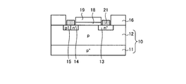
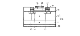
- 2 to 10 are cross-sectional views showing the state in the middle of manufacturing the silicon carbide semiconductor device according to the first embodiment.
- ap + -type semiconductor substrate (p + -type silicon carbide substrate) 11 made of silicon carbide (SiC) as a semiconductor material is prepared.
- a p-type having as a main surface a surface (preferably a surface inclined at about 0 degree to 4 degrees) inclined at about 0 degrees to 8 degrees from the (000-1) plane of 4H-SiC.
- the p-type epitaxial layer 12 having a thickness of, for example, about 5 ⁇ m to 10 ⁇ m is grown.
- the acceptor density of the p-type epitaxial layer 12 may be, for example, 1 ⁇ 10 16 cm ⁇ 3 .
- a p-type SiC epitaxial substrate 10 in which the p-type epitaxial layer 12 is stacked on the p + -type silicon carbide substrate 11 is manufactured (step S1). The situation up to here is shown in FIG.
- the surface on the p-type epitaxial layer 12 side of the SiC epitaxial substrate 10 is referred to as the front surface
- the surface on the p + -type silicon carbide substrate 11 side is referred to as the back surface.
- a MOS gate metal-oxide film- A semiconductor region constituting an insulating gate made of a semiconductor is formed (step S2).
- an oxide film (SiO 2 film) 31 having a thickness of, for example, 1 ⁇ m is deposited on the front surface of the SiC epitaxial substrate 10 by, for example, low pressure CVD (Chemical Vapor Deposition).
- the oxide film 31 is patterned by photolithography to remove portions of the oxide film 31 corresponding to the formation region of the n + drain region and portions corresponding to the formation region of the n + source region.
- phosphorus (P) ions 32 are implanted into the front surface of the SiC epitaxial substrate 10 using the remaining portion of the oxide film 31 as a mask.
- the substrate temperature may be about 500 ° C.
- the acceleration energy may be multistage ion implantation at about 40 keV to 250 keV
- the implantation amount may be about 2 ⁇ 10 20 cm ⁇ 3 .
- n-type impurity regions 13a and 14a are formed apart from each other in the surface layer on the front surface of SiC epitaxial substrate 10. The state up to here is shown in FIG.
- an oxide film 33 of, eg, a 1 ⁇ m thickness is deposited by, eg, low pressure CVD.
- the oxide film 33 is patterned by photolithography to remove the portion of the oxide film 33 corresponding to the formation region of the p + ground region.
- aluminum (Al) ions 34 are ion-implanted on the front surface of the SiC epitaxial substrate 10 using the remaining portion of the oxide film 33 as a mask.
- the ion implantation conditions of the aluminum ion 34 may be, for example, a substrate temperature of about 500 ° C., an acceleration energy of multistage ion implantation within a range of about 40 keV to 200 keV, and a dose of about 2 ⁇ 10 20 cm ⁇ 3 .
- p-type impurity region 15a is formed in the surface layer on the front surface of SiC epitaxial substrate 10 on the opposite side of impurity region 14a with respect to impurity region 13a so as to be in contact with impurity region 14a. .
- the situation up to here is shown in FIG.
- annealing is performed at a temperature of 1600 ° C. for 5 minutes in an argon atmosphere, for example, to activate impurity regions 13a, 14a, 15a.
- impurity regions 13a, 14a, 15a are activated in the active region (active region).
- P + ground region 15 is formed.
- the active region is a region through which current flows when in the on state. The state up to here is shown in FIG.
- a field oxide film 16 of, eg, a 0.5 ⁇ m thickness is deposited on the front surface of the SiC epitaxial substrate 10 by, eg, low pressure CVD.
- field oxide film 16 is selectively removed by photolithography to expose the front surface of SiC epitaxial substrate 10 in active region 17.
- the removal of the field oxide film 16 may be performed by wet etching, for example.
- a first heat treatment (oxynitridation) is performed in an oxidizing atmosphere made of an oxide compound containing, for example, nitrogen (step S3).
- the first heat treatment is performed, for example, at a temperature of about 1300 ° C. for about 100 minutes in an atmosphere in which the flow ratio of nitrous oxide (N 2 O) to nitrogen is 1: 5.
- a second heat treatment is performed at a temperature of about 1000 ° C. for about 30 minutes (step S4).
- a gate insulating film 18 having a thickness of, for example, about 50 nm is formed on the front surface of the SiC epitaxial substrate 10 in the active region 17.
- the atmosphere of the second heat treatment may be a mixed gas atmosphere in which hydrogen is diluted with an inert gas.
- the gate electrode 19 is formed on the gate insulating film 18 (step S5). Specifically, for example, polycrystalline silicon having a thickness of 0.3 ⁇ m is deposited on the gate insulating film 18 by, eg, low pressure CVD. Next, polycrystalline silicon is patterned by photolithography, the polysilicon, leaving the portion covering the p-type epitaxial layer 12 as the gate electrode 19 over the n + source region 14 of n + drain region 13. Then, the resist film used for patterning the gate electrode 19 is removed. The state up to here is shown in FIG.
- step S6 After the SiC epitaxial substrate 10 is cooled to room temperature (for example, 25 ° C.), an interlayer insulating film (not shown) covering the front surface side of the SiC epitaxial substrate 10 is formed (step S6). Next, in an inert gas atmosphere, a third heat treatment for about 10 minutes at a temperature of about 800 ° C., for example, for baking the interlayer insulating film is performed (step S7).
- a contact metal 20 in contact with the semiconductor region (silicon carbide semiconductor) forming the MOS gate is formed (step S8).
- the gate insulating film 18 and the interlayer insulating film are selectively removed by photolithography to expose the contact hole where the n + drain region 13 is exposed, and the n + source region 14 and the p + ground region 15. Form contact holes.
- the removal of the gate insulating film 18 and the interlayer insulating film may be performed by wet etching using, for example, hydrofluoric acid (HF).
- an aluminum film of, eg, a 10 nm thickness and a nickel film of, eg, a 60 nm thickness are sequentially deposited to fill each contact hole, thereby forming a metal laminated film.
- the resist film used for patterning the gate insulating film 18 and the interlayer insulating film is lifted off, and the metal laminated film on the resist film is removed together with the resist film, thereby n + metal laminated film in the contact hole.
- Contact metal 20 in contact with drain region 13 and contact metal 20 in contact with n + source region 14 and p + ground region 15 are left. The state up to here is shown in FIG.
- a fourth heat treatment is performed to form an ohmic contact between the contact metal 20 and the silicon carbide semiconductor (step S9).
- the fourth heat treatment is performed in an inert gas atmosphere, for example, at a temperature of 950 ° C. for about 2 minutes to form a reaction layer (electrical contact portion: contact) 21 between the contact metal 20 and the silicon carbide semiconductor.
- the state up to here is shown in FIG.
- the third and fourth heat treatments described above are performed, for example, in an inert gas atmosphere such as nitrogen (N 2 ), helium (He), or argon (Ar).
- the temperature of the third heat treatment can be variously selected in consideration of, for example, the degree of baking of the interlayer insulating film, and the temperature of the fourth heat treatment can be variously selected in consideration of, for example, the contact resistance.
- the heat treatment temperature is higher than the first heat treatment temperature (oxidation temperature)
- the interface state density at the junction interface between the gate insulating film 18 and the silicon carbide semiconductor (p-type epitaxial layer 12) is significantly increased. There is a risk. Therefore, it is desirable that the temperatures of the third and fourth heat treatments be equal to or lower than the temperature of the first heat treatment.
- an aluminum (Al) film of, eg, a 300 nm thickness is vapor-deposited on the front surface side of the SiC epitaxial substrate 10.
- the aluminum film is selectively removed by photolithography to form the pad electrode 22 on the gate electrode 19 and the reaction layer 21 (step S10).
- the removal of the aluminum film may be performed by wet etching using, for example, phosphoric acid (H 3 PO 4 ).
- an aluminum film having a thickness of, for example, 100 nm is vapor-deposited on the back surface of SiC epitaxial substrate 10 (the back surface of p + -type silicon carbide substrate 11) to form back surface electrode 23 (step S11).
- the MOSFET is completed.
- the characteristics of the silicon carbide MOSFET manufactured under the above-described various conditions were evaluated.
- the channel mobility is approximately 35 cm 2 / Vs, which is effective to obtain desired device characteristics. It was confirmed that the threshold voltage was 4 V, indicating a sufficiently normally-off characteristic.
- the method of manufacturing a silicon carbide semiconductor device according to the second embodiment is different from the method of manufacturing a silicon carbide semiconductor device according to the first embodiment in the method of forming the gate insulating film 18.
- the gate insulating film 18 is formed as follows.
- heat treatment is performed at a temperature of, for example, about 1100 ° C. for 50 minutes in a dry oxygen atmosphere.
- the first heat treatment is performed, for example, at a temperature of about 1300 ° C. for about 30 minutes in an atmosphere in which the flow ratio of nitrous oxide and nitrogen is 1:20.
- heat treatment is performed, for example, at a temperature of about 1000 ° C. for about 30 minutes in an atmosphere containing hydrogen.
- the steps other than the step of forming gate insulating film 18 in the method for manufacturing a silicon carbide semiconductor device according to the second embodiment are the same as in the first embodiment.
- the characteristics of the silicon carbide MOSFET manufactured under the above-described various conditions were evaluated.
- the silicon carbide MOSFET manufactured by the method of manufacturing a silicon carbide semiconductor device according to the second embodiment has the same characteristics as the silicon carbide MOSFET manufactured by the method of manufacturing the silicon carbide semiconductor device according to the first embodiment. It was confirmed to show.
- the method of manufacturing a silicon carbide semiconductor device according to the third embodiment is different from the method of manufacturing a silicon carbide semiconductor device according to the first embodiment in the method of forming the gate insulating film 18.
- the gate insulating film 18 is formed as follows.
- heat treatment is performed at a temperature of about 1100 ° C. for about 50 minutes in a dry oxygen atmosphere, for example.
- the first heat treatment is performed, for example, at a temperature of about 1200 ° C. for about 30 minutes in an atmosphere in which the flow ratio of nitrogen monoxide and nitrogen is 1:10.
- a second heat treatment is performed at a temperature of about 1000 ° C. for about 30 minutes.
- the characteristics of the silicon carbide MOSFET manufactured under the above-described various conditions were evaluated.
- the silicon carbide MOSFET manufactured by the method of manufacturing a silicon carbide semiconductor device according to the third embodiment has the same characteristics as the silicon carbide MOSFET manufactured by the method of manufacturing the silicon carbide semiconductor device according to the first embodiment. It was confirmed to show.
- Embodiment 4 Next, a method of manufacturing the silicon carbide semiconductor device according to the fourth embodiment will be described.
- the method of manufacturing a silicon carbide semiconductor device according to the fourth embodiment is different from the method of manufacturing a silicon carbide semiconductor device according to the first embodiment in the method of forming the gate insulating film 18.
- the gate insulating film 18 is formed as follows.
- a thickness (for example, a thickness close to 50 nm and a thickness less than 50 nm) thinner than the desired thickness of the gate insulating film 18 is (1)
- An insulating film is formed by a deposition method.
- the first insulating film and the SiC epitaxial substrate 10 are subjected to a first heat treatment (oxynitridation) for about 30 minutes, for example, at a temperature of about 1300 ° C. in an atmosphere with a flow ratio of nitrous oxide to nitrogen of 1:20.
- a second heat treatment is performed at a temperature of about 1000 ° C. for about 30 minutes.
- a gate insulating film 18 having a total thickness of about 50 nm, in which the first and second insulating films are stacked, is formed.
- the method of depositing the first insulating film is not particularly limited.
- the first insulating film may be deposited by a CVD method using silane (SiH 4 ) or TEOS (tetraethoxysilane).
- the steps other than the step of forming gate insulating film 18 in the method for manufacturing a silicon carbide semiconductor device according to the fourth embodiment are the same as in the first embodiment.
- the characteristics of the silicon carbide MOSFET manufactured under the above-described various conditions were evaluated.
- the silicon carbide MOSFET manufactured by the method of manufacturing a silicon carbide semiconductor device according to the fourth embodiment has the same characteristics as the silicon carbide MOSFET manufactured by the method of manufacturing the silicon carbide semiconductor device according to the first embodiment. It was confirmed to show.
- FIG. 11 is a cross-sectional view showing the configuration of a MOS capacitor manufactured by the method for manufacturing a silicon carbide semiconductor device according to the example.
- FIG. 12 is a characteristic diagram showing the relationship between the interface state density at the MOS gate interface and the flat band voltage of the MOS gate. According to the manufacturing method of the silicon carbide semiconductor device concerning Embodiment 1 mentioned above, the MOS capacitor was produced as a sample for verification on the above-mentioned conditions illustrated to Embodiment 1 (the following is considered as an example).
- the complex MOS gate structure is, for example, an element structure in which a channel is formed in the vicinity of the surface of the SiC epitaxial substrate when in the on state.
- FIG. 13 shows an example of a semiconductor device provided with a complicated MOS gate structure.
- FIG. 13 is a cross-sectional view showing an example of a semiconductor device provided with a complex MOS gate structure according to the present invention.
- an n-type epitaxial layer 42 is formed on the front surface of the n + -type silicon carbide substrate 41.
- the impurity concentration of n-type epitaxial layer 42 is lower than the impurity concentration of n + -type silicon carbide substrate 41.
- a plurality of p-type regions 46 are selectively formed in the n-type epitaxial layer 42.
- the p type region 46 is exposed on the surface of the n type epitaxial layer 42 opposite to the n + type silicon carbide substrate 41 side.
- a p-type SiC layer 47 having a concentration lower than that of p-type region 46 is formed over the surfaces of n-type epitaxial layer 42 and p-type region 46.
- An n-type region 43 penetrating the p-type SiC layer 47 in the depth direction and reaching the n-type epitaxial layer 42 is formed in the p-type SiC layer 47 on the n-type epitaxial layer 42 where the p-type region 46 is not formed. .
- the n-type epitaxial layer 42 and the n-type region 43 are n-type drift regions.
- the impurity concentration of the n-type region 43 is desirably higher than that of the n-type epitaxial layer 42.
- an n + source region 44 and ap + contact region 45 are formed in contact with each other.
- the n + source region 44 and the p + contact region 45 are exposed on the side opposite to the p-type region 46 side of the p-type SiC layer 47.
- the n + source region 44 is formed apart from the n-type region 43.
- the p + -type contact region 45 is located on the opposite side to the n-type region 43 side of the n + -type source region 44.
- the impurity concentration of the p + -type contact region 45 is higher than the impurity concentration of the p-type SiC layer 47.
- the portion excluding the n + source region 44, the p + contact region 45 and the n type region 43 of the p type SiC layer 47 becomes a p type base region together with the p type region 46.
- a source electrode 48 is formed on the surfaces of the n + source region 44 and the p + contact region 45.
- the gate electrode 19 is formed on the surface of the p-type SiC layer 47 and the n-type region 43 between the adjacent n + source regions 44 via the gate insulating film 18. Gate electrode 19 is electrically insulated from source electrode 48 by an interlayer insulating film (not shown). Further, on the back surface of the n + -type silicon carbide substrate 41, the drain electrode 49 in contact with the n + -type silicon carbide substrate 41 is formed.
- the MOS capacitor produced as an example was produced as follows. First, a SiC epitaxial substrate 7 in which the n-type epitaxial layer 2 is stacked on the n + -type silicon carbide substrate 1 was prepared (step S1). Next, after performing a first heat treatment for 100 minutes at a temperature of 1300 ° C. in a nitrous oxide (N 2 O) atmosphere to form gate insulating film 3 on the front surface of SiC epitaxial substrate 7 (step S3) A second heat treatment was performed for 30 minutes at a temperature of 1000 ° C. in a hydrogen (H 2 ) atmosphere (step S4).
- a SiC epitaxial substrate 7 in which the n-type epitaxial layer 2 is stacked on the n + -type silicon carbide substrate 1 was prepared (step S1).
- N 2 O nitrous oxide
- a second heat treatment was performed for 30 minutes at a temperature of 1000 ° C. in a hydrogen (H 2 ) atmosphere (step S4).
- step S5 heat treatment was performed in a nitrogen (N 2 ) atmosphere assuming the third heat treatment for baking the interlayer insulating film and the fourth heat treatment for forming the contact.
- step S5 heat treatment was performed in a nitrogen (N 2 ) atmosphere assuming the third heat treatment for baking the interlayer insulating film and the fourth heat treatment for forming the contact.
- step S5 the gate electrode 4 having a dot-like planar shape was formed (step S5).
- the back electrode 5 is formed on the entire back surface of the SiC epitaxial substrate 7 (step S11) to fabricate the MOS capacitor shown in FIG.
- Comparative Example 1 the atmosphere of the MOS capacitor (hereinafter referred to as Comparative Example 1) not to carry out the second heat treatment (Step S4), and the third and fourth heat treatments (Steps S7 and S9) are inert gas (nitrogen) and hydrogen.
- the configuration other than the heat treatment conditions of Comparative Examples 1 and 2 is the same as that of the example.
- the interface state density at the MOS gate interface and the flat band voltage of the MOS gate change depending on the presence or absence of the second heat treatment and the gas species of the atmosphere of the third and fourth heat treatments. Further, it was confirmed that the example can reduce both the interface state density at the MOS gate interface and the flat band voltage of the MOS gate more than the comparative examples 1 and 2. That is, as described in the method of manufacturing a semiconductor device according to each of the embodiments, the third and fourth heat treatments are performed by performing the second heat treatment in an atmosphere containing hydrogen when forming the gate insulating film and after forming the gate insulating film. It has been confirmed that the interface state density at the MOS gate interface and the flat band voltage of the MOS gate can be controlled by appropriately selecting the atmosphere of and appropriately combining these heat treatments.
- nitrogen is contained in forming the gate oxide film on the main surface of the silicon carbide semiconductor with the surface inclined at 0 degrees to 8 degrees from the (000-1) surface.
- first heat treatment in an atmosphere
- nitrogen atoms contained in the atmosphere contribute to termination of dangling bonds of silicon atoms in the gate insulating film or at the MOS gate interface.
- the interface state density at the MOS gate interface can be reduced.
- second heat treatment in an atmosphere containing hydrogen after the first heat treatment, dangling bonds of silicon atoms remaining after oxidation are terminated by hydrogen atoms, and the interface state density at the MOS gate interface is further reduced.
- the present invention is not limited to the above-described embodiment, and various modifications can be made without departing from the spirit of the present invention.
- the fourth heat treatment for forming an ohmic contact which generally requires the highest temperature in the heat treatment in the step performed after the formation of the gate insulating film is described as an example.
- similar effects can be obtained even when another heat treatment performed after the formation of the gate insulating film is performed in an inert gas atmosphere.
- other heat treatments performed after the formation of the gate insulating film include the heat treatment for forming a polysilicon layer to be a gate electrode, reducing the resistance, and the heat treatment for planarizing the interlayer insulating film, etc. It is various heat treatments.
- the method for manufacturing a silicon carbide semiconductor device according to the present invention is useful for a semiconductor device having a MOS gate.
Landscapes
- Insulated Gate Type Field-Effect Transistor (AREA)
- Electrodes Of Semiconductors (AREA)
- Recrystallisation Techniques (AREA)
Abstract
MOS型炭化珪素半導体装置を作製するにあたって、亜酸化窒素や一酸化窒素など窒素を含む酸化化合物からなる酸化雰囲気において第1熱処理(酸窒化)を行った後(ステップS3)、水素を含む第2熱処理を行うことにより(ステップS4)、SiCエピタキシャル基板のおもて面にゲート絶縁膜を形成する。次に、ゲート電極を形成し(ステップS5)、層間絶縁膜を形成した後(ステップS6)、層間絶縁膜の焼き締めのための第3熱処理を行う(ステップS7)。次に、コンタクトメタルを形成した後(ステップS8)、コンタクトメタルと炭化珪素半導体との反応層を形成するための第4熱処理を行う(ステップS9)。第3,4熱処理は、窒素、ヘリウムまたはアルゴンなどの不活性ガス雰囲気で行う。このようにすることで、ノーマリオフ特性を示し、かつ界面準位密度を低減させることができる炭化珪素半導体装置の製造方法を提供することができる。
Description
この発明は、炭化珪素半導体装置の製造方法に関する。
炭化珪素(SiC)を半導体材料とした半導体基板(炭化珪素基板)を用いた次世代半導体デバイスの研究開発が進められている。炭化珪素は、シリコン(Si)と同様に熱酸化でゲート絶縁膜を形成可能である。しかし、基板主面の面方位や熱酸化方法によって、MOSゲート(金属-酸化膜-半導体からなる絶縁ゲート)を構成するゲート絶縁膜と炭化珪素基板との接合界面(以下、MOSゲート界面とする)付近でのチャネル移動度に違いが生じるという特性がある。チャネル移動度を代替的に評価する指標として界面準位密度がある。一般的には、MOSゲート界面での界面準位密度が小さいほど、チャネル移動度が大きくなる傾向にあることが知られている。
炭化珪素基板上にゲート絶縁膜を形成する方法として、亜酸化窒素(N2O)や一酸化窒素(NO)など窒素を含む雰囲気を用いた熱酸化を行う方法が知られている。この方法では、酸化と同時に窒化が起こり、雰囲気中に含まれる窒素原子がゲート絶縁膜中やMOSゲート界面のシリコン原子の未結合手(ダングリングボンド)の終端化に寄与し、MOSゲート界面での界面準位密度を低減する効果があるとされている。さらに、この酸化直後に水素(H2)を含む雰囲気でアニール(熱処理)し、酸化後に残るシリコン原子のダングリングボンドが水素原子によって終端され、MOSゲート界面での界面準位密度がさらに低減される。
また、炭化珪素基板を用いた半導体デバイスの製造工程では、ゲート絶縁膜形成後に、ゲート電極の形成および低抵抗化のための熱処理や、層間絶縁膜の形成および焼締めのための熱処理、コンタクトメタルの形成およびコンタクトメタルと炭化珪素半導体(炭化珪素基板)との反応層(電気的接触部)の形成のための熱処理など、熱処理工程が必須である。ゲート酸化膜と炭化珪素基板との接合界面での界面準位密度等の界面特性は、ゲート絶縁膜の形成工程において所定条件を満たすように設定されるが、ゲート絶縁膜形成後の熱処理によって変化することが知られている(例えば、下記特許文献1参照。)。
下記特許文献1には、炭化珪素基板の(000-1)面上にMOSゲートを備えたMOSFET(絶縁ゲート型電界効果トランジスタ)を製造するにあたって、コンタクトメタルと炭化珪素半導体との反応層を形成するための熱処理を、不活性ガス雰囲気ではなく、不活性ガスと水素との混合ガス雰囲気(フォーミングガス(FG)雰囲気)で行うことにより、MOSゲート界面での界面準位密度の増加を抑え、かつコンタクト抵抗を低減する方法が提案されている。
しかしながら、炭化珪素基板を用いた半導体デバイスでは、上述したようにゲート絶縁膜形成後に高温の熱処理が必須であり、この熱処理の条件(温度や雰囲気など)によって半導体デバイスの特性が変化してしまう。このため、ゲート絶縁膜の形成条件に加えて、ゲート絶縁膜形成後に行う熱処理の条件も併せて検討する必要がある。例えば、半導体デバイスは、ゲートに信号が入力されていない状態のときにオフ状態(以下、ノーマリオフとする)であることが望ましい。すなわち、半導体デバイスのしきい値電圧は正の値であることが望ましい。
しきい値電圧はフラットバンド電圧を引数とする関数で表され、しきい値電圧を正の値とするには、フラットバンド電圧が正の値であることが望ましい。しかしながら、上述したゲート絶縁膜の形成方法、すなわち炭化珪素基板の(000-1)面や(11-20)面を亜酸化窒素や一酸化窒素などの窒素を含むガス雰囲気中で熱酸化し、さらに水素を含む雰囲気のアニールを行うことでゲート酸化膜と炭化珪素基板との接合界面での界面準位密度を低減させる方法では、フラットバンド電圧は負の値となり、ゲートに信号が入力されていない状態のときに半導体デバイスがオン状態(ノーマリオン)となってしまう。
この発明は、上述した従来技術による問題点を解消するため、ノーマリオフ特性を示し、かつ界面準位密度を低減させることができる炭化珪素半導体装置の製造方法を提供することを目的とする。
上述した課題を解決し、本発明の目的を達成するため、この発明にかかる炭化珪素半導体装置の製造方法は、次の特徴を有する。炭化珪素からなる半導体基板に、窒素を含む酸化化合物からなる酸化雰囲気で第1熱処理を行った後、水素を含む雰囲気で第2熱処理を行うことにより、前記半導体基板の(000-1)面または(11-20)面から0度以上8度以下の範囲内で傾けた面上にゲート絶縁膜を形成する工程を行う。そして、前記ゲート絶縁膜の形成後に行う第3熱処理を不活性ガス雰囲気で行う。
また、この発明にかかる炭化珪素半導体装置の製造方法は、上述した発明において、前記第3熱処理の温度は、前記第1熱処理の温度以下であることを特徴とする。
また、この発明にかかる炭化珪素半導体装置の製造方法は、上述した発明において、前記第1熱処理を亜酸化窒素または一酸化窒素を含む雰囲気で行うことを特徴とする。
また、この発明にかかる炭化珪素半導体装置の製造方法は、上述した発明において、前記ゲート絶縁膜を形成する工程では、前記第1熱処理前に、前記半導体基板の、前記ゲート絶縁膜が形成される側の面を乾燥酸素雰囲気で酸化することを特徴とする。
また、この発明にかかる炭化珪素半導体装置の製造方法は、上述した発明において、前記ゲート絶縁膜を形成する工程では、前記第1熱処理前に、前記ゲート絶縁膜を構成する、当該ゲート絶縁膜よりも厚さの薄い絶縁膜を堆積させることを特徴とする。
また、この発明にかかる炭化珪素半導体装置の製造方法は、上述した発明において、前記不活性ガス雰囲気は、窒素、ヘリウムまたはアルゴンを含む雰囲気であることを特徴とする。
また、この発明にかかる炭化珪素半導体装置の製造方法は、上述した発明において、前記第3熱処理は、前記半導体基板と当該半導体基板に接する金属膜との電気的接触部を形成するための工程、前記ゲート絶縁膜上に形成されるゲート電極の低抵抗化のための工程、または、前記金属膜と前記ゲート電極とを電気的に絶縁する層間絶縁膜の焼き締めのための工程で行われることを特徴とする。
上述した発明によれば、ゲート絶縁膜形成後の工程において従来より行われている熱処理の雰囲気を不活性ガス雰囲気とすることによって、炭化珪素半導体基板の(000-1)面または(11-20)面から0度~8度程度傾けた面を主面に窒素を含む雰囲気での熱酸化によりゲート絶縁膜を形成した場合においても、新たな工程を追加することなく、4×1011cm-2eV-1以下の低い界面準位密度と、1V以上の正のフラットバンド電圧とを有する炭化珪素半導体装置を作製することができる。
本発明にかかる炭化珪素半導体装置の製造方法によれば、ノーマリオフ特性を示し、かつ界面準位密度を低減させることができるという効果を奏する。
以下に添付図面を参照して、この発明にかかる炭化珪素半導体装置の製造方法の好適な実施の形態を詳細に説明する。本明細書および添付図面においては、nまたはpを冠記した層や領域では、それぞれ電子または正孔が多数キャリアであることを意味する。また、nやpに付す+および-は、それぞれそれが付されていない層や領域よりも高不純物濃度および低不純物濃度であることを意味する。また、ミラー指数の表記において、"-"はその直後の指数につくバーを意味しており、指数の前に"-"を付けることで負の指数を表している。なお、以下の実施の形態の説明および添付図面において、同様の構成には同一の符号を付し、重複する説明を省略する。
(実施の形態1)
実施の形態1にかかる炭化珪素半導体装置の製造方法として、横型の炭化珪素MOSFETを製造する方法について詳細に説明する。図1は、実施の形態1にかかる半導体装置の製造方法の概要を示すフローチャートである。図2~10は、実施の形態1にかかる炭化珪素半導体装置の製造途中の状態を示す断面図である。まず、炭化珪素(SiC)を半導体材料としたp+型半導体基板(p+型炭化珪素基板)11を用意する。p+型炭化珪素基板11として、例えば4H-SiCの(000-1)面から0度~8度程度傾けた面(好ましくは0度~4度程度傾けた面)を主面とするp型の4H-SiC基板を用意してもよい。
実施の形態1にかかる炭化珪素半導体装置の製造方法として、横型の炭化珪素MOSFETを製造する方法について詳細に説明する。図1は、実施の形態1にかかる半導体装置の製造方法の概要を示すフローチャートである。図2~10は、実施の形態1にかかる炭化珪素半導体装置の製造途中の状態を示す断面図である。まず、炭化珪素(SiC)を半導体材料としたp+型半導体基板(p+型炭化珪素基板)11を用意する。p+型炭化珪素基板11として、例えば4H-SiCの(000-1)面から0度~8度程度傾けた面(好ましくは0度~4度程度傾けた面)を主面とするp型の4H-SiC基板を用意してもよい。
次に、p+型炭化珪素基板11のおもて面に、例えば5μm以上10μm以下程度の厚さのp型エピタキシャル層12を成長させる。p型エピタキシャル層12のアクセプター密度は、例えば1×1016cm-3であってもよい。これによって、p+型炭化珪素基板11上にp型エピタキシャル層12が積層されてなるp型のSiCエピタキシャル基板10が作製される(ステップS1)。ここまでの状態が図2に示されている。以下、SiCエピタキシャル基板10のp型エピタキシャル層12側の面をおもて面とし、p+型炭化珪素基板11側の面(すなわち、p+型炭化珪素基板11の裏面)を裏面とする。
次に、SiCエピタキシャル基板10のおもて面(すなわちp型エピタキシャル層12の、p+型炭化珪素基板11側に対して反対側の表面)の表面層に、MOSゲート(金属-酸化膜-半導体からなる絶縁ゲート)を構成する半導体領域を形成する(ステップS2)。具体的には、例えば減圧CVD(Chemical Vapor Deposition)法により、SiCエピタキシャル基板10のおもて面上に、例えば厚さ1μmの酸化膜(SiO2膜)31を堆積する。次に、フォトリソグラフィにより酸化膜31をパターニングし、酸化膜31の、n+ドレイン領域の形成領域に対応する部分およびn+ソース領域の形成領域に対応する部分をそれぞれ除去する。
次に、酸化膜31の残部をマスクとして、SiCエピタキシャル基板10のおもて面にリン(P)イオン32をイオン注入する。リンイオン32のイオン注入条件は、例えば、基板温度を500℃程度とし、加速エネルギーを40keV~250keV程度での多段イオン注入とし、注入量を2×1020cm-3程度としてもよい。これによって、SiCエピタキシャル基板10のおもて面の表面層に、互いに離れてn型の不純物領域13a,14aが形成される。ここまでの状態が図3に示されている。
次に、酸化膜31の残部を除去した後、例えば減圧CVD法により、例えば厚さ1μmの酸化膜33を堆積する。次に、フォトリソグラフィにより酸化膜33をパターニングし、酸化膜33の、p+グラウンド領域の形成領域に対応する部分を除去する。次に、酸化膜33の残部をマスクとして、SiCエピタキシャル基板10のおもて面にアルミニウム(Al)イオン34をイオン注入する。
アルミニウムイオン34のイオン注入条件は、例えば、基板温度を500℃程度とし、加速エネルギーを40keV~200keV程度の範囲内での多段イオン注入とし、注入量を2×1020cm-3程度としてもよい。これによって、SiCエピタキシャル基板10のおもて面の表面層に、不純物領域14aの、不純物領域13a側に対して反対側に、不純物領域14aに接するようにp型の不純物領域15aが形成される。ここまでの状態が図4に示されている。
次に、酸化膜33の残部を除去した後、例えば、アルゴン雰囲気中において、1600℃の温度で5分間のアニールを行い、不純物領域13a,14a,15aを活性化させる。これによって、アクティブ領域(活性領域)に、不純物領域13aが活性化されてなるn+ドレイン領域13、不純物領域14aが活性化されてなるn+ソース領域14、および不純物領域15aが活性化されてなるp+グラウンド領域15が形成される。アクティブ領域とは、オン状態のときに電流が流れる領域である。ここまでの状態が図5に示されている。
次に、例えば減圧CVD法により、SiCエピタキシャル基板10のおもて面に、例えば厚さ0.5μmのフィールド酸化膜16を堆積する。次に、フォトリソグラフィによりフィールド酸化膜16を選択的に除去し、アクティブ領域17におけるSiCエピタキシャル基板10のおもて面を露出させる。フィールド酸化膜16の除去は、例えばウェットエッチングにより行ってもよい。これにより、アクティブ領域17において、n+ドレイン領域13、n+ソース領域14およびp+グラウンド領域15が露出される。ここまでの状態が図6に示されている。
次に、SiCエピタキシャル基板10を洗浄した後、例えば窒素を含む酸化化合物からなる酸化雰囲気において第1熱処理(酸窒化)を行う(ステップS3)。具体的には、第1熱処理は、例えば亜酸化窒素(N2O)と窒素との流量比が1:5の雰囲気において、例えば1300℃程度の温度で100分間程度行う。次に、水素(H2)を含む雰囲気において、例えば1000℃程度の温度で30分間程度の第2熱処理を行う(ステップS4)。この第1,2熱処理によって、アクティブ領域17におけるSiCエピタキシャル基板10のおもて面上に、例えば50nm程度の厚さのゲート絶縁膜18を形成する。第2熱処理の雰囲気は、水素を不活性ガスで希釈した混合ガス雰囲気であってもよい。
次に、ゲート絶縁膜18上に、ゲート電極19を形成する(ステップS5)。具体的には、例えば減圧CVD法により、ゲート絶縁膜18上に例えば厚さ0.3μmの多結晶シリコンを堆積する。次に、フォトリソグラフィにより多結晶シリコンをパターニングし、多結晶シリコンの、n+ドレイン領域13からn+ソース領域14にわたってp型エピタキシャル層12を覆う部分をゲート電極19として残す。そして、ゲート電極19のパターニングに用いたレジスト膜を除去する。ここまでの状態が図7に示されている。
次に、SiCエピタキシャル基板10を室温(例えば25℃)まで冷却した後、SiCエピタキシャル基板10のおもて面側を覆う層間絶縁膜(不図示)を形成する(ステップS6)。次に、不活性ガス雰囲気において、層間絶縁膜の焼き締めのための例えば800℃程度の温度での10分間程度の第3熱処理を行う(ステップS7)。
次に、MOSゲートを構成する半導体領域(炭化珪素半導体)に接するコンタクトメタル20を形成する(ステップS8)。具体的には、フォトリソグラフィによりゲート絶縁膜18および層間絶縁膜を選択的に除去し、n+ドレイン領域13が露出されたコンタクトホールと、n+ソース領域14およびp+グラウンド領域15が露出されたコンタクトホールとを形成する。ゲート絶縁膜18および層間絶縁膜の除去は、例えばフッ酸(HF)を用いたウェットエッチングにより行ってもよい。
次に、各コンタクトホールを埋め込むように、例えば厚さ10nmのアルミニウム膜と、例えば厚さ60nmのニッケル膜とを順に蒸着して金属積層膜を形成する。次に、ゲート絶縁膜18および層間絶縁膜のパターニングに用いたレジスト膜をリフトオフして、レジスト膜とともにレジスト膜上の金属積層膜を除去することにより、コンタクトホール内の金属積層膜を、n+ドレイン領域13に接するコンタクトメタル20、および、n+ソース領域14およびp+グラウンド領域15に接するコンタクトメタル20として残す。ここまでの状態が図8に示されている。
次に、コンタクトメタル20と炭化珪素半導体とのオーミックコンタクトを形成するための第4熱処理を行う(ステップS9)。具体的には、不活性ガス雰囲気において例えば950℃の温度で2分間程度の第4熱処理を行い、コンタクトメタル20と炭化珪素半導体との反応層(電気的接触部:コンタクト)21を形成する。ここまでの状態が図9に示されている。
上述した第3,4熱処理は、例えば、窒素(N2)、ヘリウム(He)またはアルゴン(Ar)などの不活性ガス雰囲気で行う。第3熱処理の温度は例えば層間絶縁膜の焼き締め具合などを考慮して種々選択可能であり、第4熱処理の温度は例えばコンタクト抵抗などを考慮して種々選択可能であるが、第3,4熱処理の温度を第1熱処理の温度(酸化温度)よりも高くした場合、ゲート絶縁膜18と炭化珪素半導体(p型エピタキシャル層12)との接合界面での界面準位密度の大幅な増加を招く虞がある。このため、第3,4熱処理の温度は、第1熱処理の温度以下であることが望ましい。
次に、SiCエピタキシャル基板10のおもて面側に、例えば厚さ300nmのアルミニウム(Al)膜を蒸着する。次に、フォトリソグラフィによりアルミニウム膜を選択的に除去し、ゲート電極19および反応層21上にパッド電極22を形成する(ステップS10)。アルミニウム膜の除去は、例えばリン酸(H3PO4)を用いたウェットエッチングにより行ってもよい。その後、SiCエピタキシャル基板10の裏面(p+型炭化珪素基板11の裏面)に例えば厚さ100nmのアルミニウム膜を蒸着して裏面電極23を形成することにより(ステップS11)、図10に示す炭化珪素MOSFETが完成する。
次に、上述した実施の形態1にかかる炭化珪素半導体装置の製造方法に従い、例示した上記諸条件で作製された炭化珪素MOSFETの特性を評価した。その結果、上述した実施の形態1にかかる炭化珪素半導体装置の製造方法によって炭化珪素MOSFETを作製することにより、チャネル移動度は約35cm2/Vsと所望の素子特性が得られる程度に実効的な値となり、しきい値電圧は4Vと十分なノーマリオフ特性を示すことが確認された。
(実施の形態2)
次に、実施の形態2にかかる炭化珪素半導体装置の製造方法について説明する。実施の形態2にかかる炭化珪素半導体装置の製造方法は、ゲート絶縁膜18の形成方法が実施の形態1にかかる炭化珪素半導体装置の製造方法と異なる。具体的には、実施の形態2においては、次のようにゲート絶縁膜18を形成する。
次に、実施の形態2にかかる炭化珪素半導体装置の製造方法について説明する。実施の形態2にかかる炭化珪素半導体装置の製造方法は、ゲート絶縁膜18の形成方法が実施の形態1にかかる炭化珪素半導体装置の製造方法と異なる。具体的には、実施の形態2においては、次のようにゲート絶縁膜18を形成する。
まず、乾燥酸素雰囲気において、例えば1100℃程度の温度で50分間の熱処理(酸化)を行う。次に、亜酸化窒素と窒素との流量比が1:20の雰囲気において、例えば1300℃程度の温度で30分間程度の第1熱処理(酸窒化)を行う。次に、水素を含む雰囲気において、例えば1000℃程度の温度で30分間程度の熱処理を行う。実施の形態2にかかる炭化珪素半導体装置の製造方法の、ゲート絶縁膜18の形成工程以外の工程は実施の形態1と同様である。
このような実施の形態2にかかる炭化珪素半導体装置の製造方法に従い、例示した上記諸条件で作製された炭化珪素MOSFETの特性を評価した。その結果、実施の形態2にかかる炭化珪素半導体装置の製造方法によって作製された炭化珪素MOSFETは、実施の形態1にかかる炭化珪素半導体装置の製造方法によって作製された炭化珪素MOSFETと同様の特性を示すことが確認された。
(実施の形態3)
次に、実施の形態3にかかる炭化珪素半導体装置の製造方法について説明する。実施の形態3にかかる炭化珪素半導体装置の製造方法は、ゲート絶縁膜18の形成方法が実施の形態1にかかる炭化珪素半導体装置の製造方法と異なる。具体的には、実施の形態3においては、次のようにゲート絶縁膜18を形成する。
次に、実施の形態3にかかる炭化珪素半導体装置の製造方法について説明する。実施の形態3にかかる炭化珪素半導体装置の製造方法は、ゲート絶縁膜18の形成方法が実施の形態1にかかる炭化珪素半導体装置の製造方法と異なる。具体的には、実施の形態3においては、次のようにゲート絶縁膜18を形成する。
まず、乾燥酸素雰囲気において、例えば1100℃程度の温度で50分間程度の熱処理(酸化)を行う。次に、一酸化窒素と窒素との流量比が1:10の雰囲気において、例えば1200℃程度の温度で30分間程度の第1熱処理(酸窒化)を行う。次に、水素を含む雰囲気において、例えば1000℃程度の温度で30分間程度の第2熱処理を行う。実施の形態3にかかる炭化珪素半導体装置の製造方法の、ゲート絶縁膜18の形成工程以外の工程は実施の形態1と同様である。
このような実施の形態3にかかる炭化珪素半導体装置の製造方法に従い、例示した上記諸条件で作製された炭化珪素MOSFETの特性を評価した。その結果、実施の形態3にかかる炭化珪素半導体装置の製造方法によって作製された炭化珪素MOSFETは、実施の形態1にかかる炭化珪素半導体装置の製造方法によって作製された炭化珪素MOSFETと同様の特性を示すことが確認された。
(実施の形態4)
次に、実施の形態4にかかる炭化珪素半導体装置の製造方法について説明する。実施の形態4にかかる炭化珪素半導体装置の製造方法は、ゲート絶縁膜18の形成方法が実施の形態1にかかる炭化珪素半導体装置の製造方法と異なる。具体的には、実施の形態4においては、次のようにゲート絶縁膜18を形成する。
次に、実施の形態4にかかる炭化珪素半導体装置の製造方法について説明する。実施の形態4にかかる炭化珪素半導体装置の製造方法は、ゲート絶縁膜18の形成方法が実施の形態1にかかる炭化珪素半導体装置の製造方法と異なる。具体的には、実施の形態4においては、次のようにゲート絶縁膜18を形成する。
まず、アクティブ領域17におけるSiCエピタキシャル基板10のおもて面上に、ゲート絶縁膜18の所望の厚さよりも薄い厚さ(例えば50nmに近い厚さで、かつ50nmに満たない厚さ)の第1絶縁膜を堆積法により形成する。次に、亜酸化窒素と窒素との流量比が1:20の雰囲気において、例えば1300℃程度の温度で30分間程度の第1熱処理(酸窒化)を行い、第1絶縁膜とSiCエピタキシャル基板10との界面に数nmの厚さの第2絶縁膜を形成する。次に、水素を含む雰囲気において、例えば1000℃程度の温度で30分間程度の第2熱処理を行う。これによって、第1,2絶縁膜が積層されてなる合計50nm程度の厚さのゲート絶縁膜18を形成する。第1絶縁膜の堆積方法は、特に限定されるものではなく、例えばシラン(SiH4)やTEOS(テトラエトキシシラン)を用いてCVD法により堆積してもよい。実施の形態4にかかる炭化珪素半導体装置の製造方法の、ゲート絶縁膜18の形成工程以外の工程は実施の形態1と同様である。
このような実施の形態4にかかる炭化珪素半導体装置の製造方法に従い、例示した上記諸条件で作製された炭化珪素MOSFETの特性を評価した。その結果、実施の形態4にかかる炭化珪素半導体装置の製造方法によって作製された炭化珪素MOSFETは、実施の形態1にかかる炭化珪素半導体装置の製造方法によって作製された炭化珪素MOSFETと同様の特性を示すことが確認された。
(実施例)
次に、ゲート絶縁膜と炭化珪素半導体との接合界面(MOSゲート界面)での界面準位密度、および、MOSゲートのフラットバンド電圧について検証した。図11は、実施例にかかる炭化珪素半導体装置の製造方法により製造されるMOSキャパシタの構成を示す断面図である。図12は、MOSゲート界面での界面準位密度とMOSゲートのフラットバンド電圧との関係について示す特性図である。上述した実施の形態1にかかる炭化珪素半導体装置の製造方法に従い、実施の形態1に例示した上記諸条件で、検証用試料としてMOSキャパシタを作製した(以下、実施例とする)。すなわち、複雑なMOSゲート構造を形成するための工程(ステップS2,S6,S8,S10)を行うことなく簡易に作製可能であり、かつ、実施の形態1にかかる炭化珪素MOSFETと同じMOSゲート特性を有するMOSキャパシタを作製して検証を行った。
次に、ゲート絶縁膜と炭化珪素半導体との接合界面(MOSゲート界面)での界面準位密度、および、MOSゲートのフラットバンド電圧について検証した。図11は、実施例にかかる炭化珪素半導体装置の製造方法により製造されるMOSキャパシタの構成を示す断面図である。図12は、MOSゲート界面での界面準位密度とMOSゲートのフラットバンド電圧との関係について示す特性図である。上述した実施の形態1にかかる炭化珪素半導体装置の製造方法に従い、実施の形態1に例示した上記諸条件で、検証用試料としてMOSキャパシタを作製した(以下、実施例とする)。すなわち、複雑なMOSゲート構造を形成するための工程(ステップS2,S6,S8,S10)を行うことなく簡易に作製可能であり、かつ、実施の形態1にかかる炭化珪素MOSFETと同じMOSゲート特性を有するMOSキャパシタを作製して検証を行った。
複雑なMOSゲート構造とは、例えば、オン状態のときにSiCエピタキシャル基板の表面近傍にチャネルを形成する素子構造である。図13に複雑なMOSゲート構造を備えた半導体装置の一例を示す。図13は、本発明にかかる複雑なMOSゲート構造を備えた半導体装置の一例を示す断面図である。図13に示すように、縦型のMOSFETにおいて、n+型炭化珪素基板41のおもて面にはn型エピタキシャル層42が形成される。n型エピタキシャル層42の不純物濃度は、n+型炭化珪素基板41の不純物濃度よりも低い。n型エピタキシャル層42の内部には、複数のp型領域46が選択的に形成される。p型領域46は、n型エピタキシャル層42のn+型炭化珪素基板41側に対して反対側の面に露出する。n型エピタキシャル層42およびp型領域46の表面にわたってp型領域46より低濃度のp型SiC層47が形成される。p型領域46が形成されていないn型エピタキシャル層42上のp型SiC層47に、深さ方向にp型SiC層47を貫通しn型エピタキシャル層42に達するn型領域43が形成される。n型エピタキシャル層42およびn型領域43は、n型ドリフト領域である。n型領域43の不純物濃度は、n型エピタキシャル層42よりも高いのが望ましい。
p型SiC層47の内部には、互いに接するようにn+ソース領域44およびp+型コンタクト領域45が形成される。n+ソース領域44およびp+型コンタクト領域45は、p型SiC層47のp型領域46側に対して反対側の面に露出する。n+ソース領域44は、n型領域43と離れて形成される。p+型コンタクト領域45は、n+ソース領域44のn型領域43側に対して反対側に位置する。p+型コンタクト領域45の不純物濃度は、p型SiC層47の不純物濃度よりも高い。p型SiC層47のn+ソース領域44、p+型コンタクト領域45およびn型領域43を除く部分は、p型領域46と共にp型ベース領域となる。n+ソース領域44とp+型コンタクト領域45との表面には、ソース電極48が形成される。隣り合うn+ソース領域44の間のp型SiC層47とn型領域43との表面には、ゲート絶縁膜18を介してゲート電極19が形成される。ゲート電極19は、図示省略する層間絶縁膜によって、ソース電極48と電気的に絶縁される。また、n+型炭化珪素基板41の裏面には、n+型炭化珪素基板41に接するドレイン電極49が形成される。
実施例として作製したMOSキャパシタは、具体的には、次のように作製した。まず、n+型炭化珪素基板1上にn型エピタキシャル層2が積層されてなるSiCエピタキシャル基板7を用意した(ステップS1)。次に、SiCエピタキシャル基板7のおもて面にゲート絶縁膜3を形成するために、亜酸化窒素(N2O)雰囲気において1300℃の温度で100分間の第1熱処理を行った後(ステップS3)、水素(H2)雰囲気において1000℃の温度で30分間の第2熱処理を行った(ステップS4)。次に、層間絶縁膜の焼き締めのための第3熱処理と、コンタクト形成のための第4熱処理とを想定した窒素(N2)雰囲気による熱処理を行った(ステップS7,S9)。次に、ドット状の平面形状を有するゲート電極4を形成した(ステップS5)。その後、SiCエピタキシャル基板7の裏面全面に裏面電極5を形成することにより(ステップS11)、図11に示すMOSキャパシタを作製した。
比較として、第2熱処理(ステップS4)を実施しないMOSキャパシタ(以下、比較例1とする)、および、第3,4熱処理(ステップS7,S9)の雰囲気を不活性ガス(窒素)と水素との混合ガス雰囲気(FG雰囲気)としたMOSキャパシタ(以下、比較例2とする)を作製した。すなわち、比較例1では、亜酸化窒素雰囲気での第1熱処理および窒素雰囲気での第3,4熱処理の順で熱処理を行った。比較例2では、亜酸化窒素雰囲気での第1熱処理、水素雰囲気での第2熱処理およびFG雰囲気での第3,4熱処理の順で熱処理を行った。比較例1,2の熱処理条件以外の構成は実施例と同様である。
そして、実施例および比較例1,2の各MOSキャパシタについて、それぞれゲート電極4と裏面電極5との間に容量-電圧(C-V)メーター6を接続し、C-Vメーター6の測定結果に基づいてMOSゲート界面での界面準位密度およびMOSゲートのフラットバンド電圧を算出した。その結果を図12に示す。
図12に示すように、第2熱処理(水素雰囲気処理)の有無で比較した場合、第2熱処理を行った実施例(●印)に対して、第2熱処理を行っていない比較例1(▲印)はMOSゲート界面での界面準位密度が大きいことが確認された。また、第3,4熱処理の雰囲気のガス種の違いで比較した場合、不活性ガス雰囲気で第3,4熱処理を行った実施例(●印)は、MOSゲートのフラットバンド電圧が正の値となった。それに対して、不活性ガスと水素とを混合したFG雰囲気で第3,4熱処理を行った比較例2(◆印)は、MOSゲートのフラットバンド電圧が負の値になることが確認された。
このように、第2熱処理の有無や、第3,4熱処理の雰囲気のガス種によって、MOSゲート界面での界面準位密度、および、MOSゲートのフラットバンド電圧が変化することが確認された。また、実施例は、比較例1,2よりもMOSゲート界面での界面準位密度とMOSゲートのフラットバンド電圧とをともに低減することができることが確認された。すなわち、各実施の形態にかかる半導体装置の製造方法で説明したように、ゲート絶縁膜の形成時に水素を含む雰囲気での第2熱処理を行い、かつゲート絶縁膜の形成後に行う第3,4熱処理の雰囲気を適切に選択し、これらの熱処理を適宜組み合わせることによって、MOSゲート界面での界面準位密度、MOSゲートのフラットバンド電圧を制御可能であることが確認された。
以上、説明したように、各実施の形態によれば、炭化珪素半導体の(000-1)面から0度~8度程度傾けた面を主面にゲート酸化膜を形成するにあたって、窒素を含む雰囲気で第1熱処理を行うことにより、酸化と同時に窒化が起こり、雰囲気中に含まれる窒素原子がゲート絶縁膜中やMOSゲート界面のシリコン原子の未結合手(ダングリングボンド)の終端化に寄与し、MOSゲート界面での界面準位密度を低減することができる。また、第1熱処理後に、水素を含む雰囲気で第2熱処理を行うことにより、酸化後に残るシリコン原子のダングリングボンドが水素原子によって終端され、MOSゲート界面での界面準位密度をさらに低減することができる。これにより、4×1011cm-2eV-1以下の低い界面準位密度が得られ、実効的なチャネル移動度を得ることができる。そして、ゲート絶縁膜形成後に行う工程において省略することのできない熱処理(第3,4熱処理)の雰囲気を不活性ガス雰囲気とすることで、1V以上の正のフラットバンド電圧とすることができ、ノーマリオフ特性を得ることができる。したがって、新たに特別な工程を追加することなく、実効的なチャネル移動度とノーマリオフ特性とを有する炭化珪素半導体装置を提供することができる。
以上において本発明は、上述した実施の形態に限らず、本発明の趣旨を逸脱しない範囲で種々変更可能である。例えば、上述した各実施の形態では、ゲート絶縁膜形成後に行う工程における熱処理の中で一般的に一番高い温度が必要とされているオーミックコンタクトを形成するための第4熱処理を例にして説明しているが、ゲート絶縁膜形成後に行う他の熱処理を不活性ガス雰囲気で行った場合においても同様の効果を得ることができる。具体的には、ゲート絶縁膜形成後に行う他の熱処理とは、ゲート電極となるポリシリコン層の形成および低抵抗化のための熱処理や、層間絶縁膜を平坦化するための熱処理等も含めた各種熱処理である。
また、上述した各実施の形態では、p+型半導体基板を用いた横型の炭化珪素MOSFETを製造する場合を例に説明しているが、これに限定されるものではなく、n+型半導体基板を用いた縦型の炭化珪素MOSFETなど高耐圧化構造を有する炭化珪素半導体装置など、MOSゲートを有する種々半導体装置に適用する場合においても同様の効果が得られる。また、上述した各実施の形態は、4H-SiCの(11-20)面から0度~8度程度傾けた面を主面とする4H-SiC基板に適用する場合においても同様の効果が得られる。また、本発明は、導電型を反転させても同様に成り立つ。
以上のように、本発明にかかる炭化珪素半導体装置の製造方法は、MOSゲートを有する半導体装置に有用である。
1 n+型炭化珪素基板
2 n型エピタキシャル層
3,18 ゲート絶縁膜
4,19 ゲート電極
5,23 裏面電極
6 C-Vメーター
7,10 SiCエピタキシャル基板
11 p+炭化珪素基板
12 p型エピタキシャル層
13 n+ドレイン領域
13a,14a,15a 不純物領域
14 n+ソース領域
15 p+グラウンド領域
16 フィールド酸化膜
17 アクティブ領域
20 コンタクトメタル
21 反応層
22 パッド電極
31,33 酸化膜
32 リンイオン
34 アルミニウムイオン
2 n型エピタキシャル層
3,18 ゲート絶縁膜
4,19 ゲート電極
5,23 裏面電極
6 C-Vメーター
7,10 SiCエピタキシャル基板
11 p+炭化珪素基板
12 p型エピタキシャル層
13 n+ドレイン領域
13a,14a,15a 不純物領域
14 n+ソース領域
15 p+グラウンド領域
16 フィールド酸化膜
17 アクティブ領域
20 コンタクトメタル
21 反応層
22 パッド電極
31,33 酸化膜
32 リンイオン
34 アルミニウムイオン
Claims (7)
- 炭化珪素からなる半導体基板に、窒素を含む酸化化合物からなる酸化雰囲気で第1熱処理を行った後、水素を含む雰囲気で第2熱処理を行うことにより、前記半導体基板の(000-1)面または(11-20)面から0度以上8度以下の範囲内で傾けた面上にゲート絶縁膜を形成する工程を含み、
前記ゲート絶縁膜の形成後に行う第3熱処理を不活性ガス雰囲気で行うことを特徴とする炭化珪素半導体装置の製造方法。 - 前記第3熱処理の温度は、前記第1熱処理の温度以下であることを特徴とする請求項1に記載の炭化珪素半導体装置の製造方法。
- 前記第1熱処理を亜酸化窒素または一酸化窒素を含む雰囲気で行うことを特徴とする請求項1に記載の炭化珪素半導体装置の製造方法。
- 前記ゲート絶縁膜を形成する工程では、前記第1熱処理前に、前記半導体基板の、前記ゲート絶縁膜が形成される側の面を乾燥酸素雰囲気で酸化することを特徴とする請求項1に記載の炭化珪素半導体装置の製造方法。
- 前記ゲート絶縁膜を形成する工程では、前記第1熱処理前に、前記ゲート絶縁膜を構成する、当該ゲート絶縁膜よりも厚さの薄い絶縁膜を堆積させることを特徴とする請求項1に記載の炭化珪素半導体装置の製造方法。
- 前記不活性ガス雰囲気は、窒素、ヘリウムまたはアルゴンを含む雰囲気であることを特徴とする請求項1に記載の炭化珪素半導体装置の製造方法。
- 前記第3熱処理は、前記半導体基板と当該半導体基板に接する金属膜との電気的接触部を形成するための工程、前記ゲート絶縁膜上に形成されるゲート電極の低抵抗化のための工程、または、前記金属膜と前記ゲート電極とを電気的に絶縁する層間絶縁膜の焼き締めのための工程で行われることを特徴とする請求項1~6のいずれか一つに記載の炭化珪素半導体装置の製造方法。
Priority Applications (1)
| Application Number | Priority Date | Filing Date | Title |
|---|---|---|---|
| US14/960,285 US9960040B2 (en) | 2013-06-21 | 2015-12-04 | Manufacturing method of silicon carbide semiconductor device |
Applications Claiming Priority (2)
| Application Number | Priority Date | Filing Date | Title |
|---|---|---|---|
| JP2013-131081 | 2013-06-21 | ||
| JP2013131081A JP6041311B2 (ja) | 2013-06-21 | 2013-06-21 | 炭化珪素半導体装置の製造方法 |
Related Child Applications (1)
| Application Number | Title | Priority Date | Filing Date |
|---|---|---|---|
| US14/960,285 Continuation US9960040B2 (en) | 2013-06-21 | 2015-12-04 | Manufacturing method of silicon carbide semiconductor device |
Publications (1)
| Publication Number | Publication Date |
|---|---|
| WO2014203904A1 true WO2014203904A1 (ja) | 2014-12-24 |
Family
ID=52104636
Family Applications (1)
| Application Number | Title | Priority Date | Filing Date |
|---|---|---|---|
| PCT/JP2014/066053 Ceased WO2014203904A1 (ja) | 2013-06-21 | 2014-06-17 | 炭化珪素半導体装置の製造方法 |
Country Status (3)
| Country | Link |
|---|---|
| US (1) | US9960040B2 (ja) |
| JP (1) | JP6041311B2 (ja) |
| WO (1) | WO2014203904A1 (ja) |
Cited By (1)
| Publication number | Priority date | Publication date | Assignee | Title |
|---|---|---|---|---|
| CN107863392A (zh) * | 2016-09-22 | 2018-03-30 | 中兴通讯股份有限公司 | 一种SiC MOS电容及其制造方法 |
Families Citing this family (3)
| Publication number | Priority date | Publication date | Assignee | Title |
|---|---|---|---|---|
| CN107437498B (zh) * | 2017-07-27 | 2020-02-21 | 湖南大学 | 碳化硅mos结构栅氧制备方法及碳化硅mos结构制备方法 |
| JP7056232B2 (ja) | 2018-02-28 | 2022-04-19 | 富士電機株式会社 | 炭化珪素半導体装置および炭化珪素半導体装置の製造方法 |
| CN115732538B (zh) * | 2022-09-08 | 2026-01-23 | 湖南三安半导体有限责任公司 | 一种半导体器件及其制作方法 |
Citations (7)
| Publication number | Priority date | Publication date | Assignee | Title |
|---|---|---|---|---|
| JPH09199497A (ja) * | 1996-01-22 | 1997-07-31 | Nippon Steel Corp | SiCの熱酸化膜の改善方法 |
| JP2006196713A (ja) * | 2005-01-13 | 2006-07-27 | National Institute Of Advanced Industrial & Technology | 半導体装置及びその作製方法並びに重水素処理装置 |
| JP2006210818A (ja) * | 2005-01-31 | 2006-08-10 | Matsushita Electric Ind Co Ltd | 半導体素子およびその製造方法 |
| JP2007242744A (ja) * | 2006-03-07 | 2007-09-20 | National Institute Of Advanced Industrial & Technology | 炭化ケイ素半導体装置の製造方法および炭化ケイ素半導体装置 |
| JP2011199132A (ja) * | 2010-03-23 | 2011-10-06 | Sumitomo Electric Ind Ltd | 半導体装置およびその製造方法 |
| JP2013004643A (ja) * | 2011-06-15 | 2013-01-07 | Mitsubishi Electric Corp | 炭化珪素半導体装置の製造方法 |
| JP2013045789A (ja) * | 2011-08-22 | 2013-03-04 | National Institute Of Advanced Industrial & Technology | 炭化ケイ素半導体装置の製造方法 |
Family Cites Families (3)
| Publication number | Priority date | Publication date | Assignee | Title |
|---|---|---|---|---|
| JP3940560B2 (ja) * | 2001-01-25 | 2007-07-04 | 独立行政法人産業技術総合研究所 | 半導体装置の製造方法 |
| US8461628B2 (en) * | 2005-03-18 | 2013-06-11 | Kovio, Inc. | MOS transistor with laser-patterned metal gate, and method for making the same |
| WO2012108142A1 (ja) * | 2011-02-07 | 2012-08-16 | シャープ株式会社 | 有機el表示装置及びその製造方法 |
-
2013
- 2013-06-21 JP JP2013131081A patent/JP6041311B2/ja active Active
-
2014
- 2014-06-17 WO PCT/JP2014/066053 patent/WO2014203904A1/ja not_active Ceased
-
2015
- 2015-12-04 US US14/960,285 patent/US9960040B2/en active Active
Patent Citations (7)
| Publication number | Priority date | Publication date | Assignee | Title |
|---|---|---|---|---|
| JPH09199497A (ja) * | 1996-01-22 | 1997-07-31 | Nippon Steel Corp | SiCの熱酸化膜の改善方法 |
| JP2006196713A (ja) * | 2005-01-13 | 2006-07-27 | National Institute Of Advanced Industrial & Technology | 半導体装置及びその作製方法並びに重水素処理装置 |
| JP2006210818A (ja) * | 2005-01-31 | 2006-08-10 | Matsushita Electric Ind Co Ltd | 半導体素子およびその製造方法 |
| JP2007242744A (ja) * | 2006-03-07 | 2007-09-20 | National Institute Of Advanced Industrial & Technology | 炭化ケイ素半導体装置の製造方法および炭化ケイ素半導体装置 |
| JP2011199132A (ja) * | 2010-03-23 | 2011-10-06 | Sumitomo Electric Ind Ltd | 半導体装置およびその製造方法 |
| JP2013004643A (ja) * | 2011-06-15 | 2013-01-07 | Mitsubishi Electric Corp | 炭化珪素半導体装置の製造方法 |
| JP2013045789A (ja) * | 2011-08-22 | 2013-03-04 | National Institute Of Advanced Industrial & Technology | 炭化ケイ素半導体装置の製造方法 |
Cited By (1)
| Publication number | Priority date | Publication date | Assignee | Title |
|---|---|---|---|---|
| CN107863392A (zh) * | 2016-09-22 | 2018-03-30 | 中兴通讯股份有限公司 | 一种SiC MOS电容及其制造方法 |
Also Published As
| Publication number | Publication date |
|---|---|
| US20160093494A1 (en) | 2016-03-31 |
| US9960040B2 (en) | 2018-05-01 |
| JP2015005669A (ja) | 2015-01-08 |
| JP6041311B2 (ja) | 2016-12-07 |
Similar Documents
| Publication | Publication Date | Title |
|---|---|---|
| JP7761711B2 (ja) | 半導体装置 | |
| JP6572423B2 (ja) | 半導体装置および半導体装置の製造方法 | |
| JP3940560B2 (ja) | 半導体装置の製造方法 | |
| JP6025007B2 (ja) | 炭化ケイ素半導体装置の製造方法 | |
| TWI642108B (zh) | 半導體裝置之製造方法 | |
| JP5584823B2 (ja) | 炭化珪素半導体装置 | |
| JP5558392B2 (ja) | 半導体装置とその製造方法 | |
| TWI311814B (en) | Silicon carbide semiconductor device and method for producing the same | |
| CN101174568B (zh) | 碳化硅半导体器件的制造方法 | |
| JP2012160485A (ja) | 半導体装置とその製造方法 | |
| JP7605241B2 (ja) | トレンチ型半導体装置の製造方法 | |
| CN105849877B (zh) | 半导体装置以及半导体装置的制造方法 | |
| JP2018206872A (ja) | 半導体装置 | |
| JP6208106B2 (ja) | 半導体装置及びその製造方法 | |
| US9960040B2 (en) | Manufacturing method of silicon carbide semiconductor device | |
| JP6500912B2 (ja) | 炭化珪素半導体装置および炭化珪素半導体装置の製造方法 | |
| JP2015142078A (ja) | 炭化ケイ素半導体装置およびその製造方法 | |
| JP7462394B2 (ja) | 炭化珪素半導体装置および炭化珪素半導体装置の製造方法 | |
| JP6780414B2 (ja) | 炭化珪素半導体装置および炭化珪素半導体装置の製造方法 | |
| JP6844176B2 (ja) | 炭化珪素半導体装置および炭化珪素半導体装置の製造方法 | |
| JP2015070192A (ja) | 半導体装置の製造方法、半導体装置 | |
| JP2017168603A (ja) | 炭化珪素半導体素子および炭化珪素半導体素子の製造方法 | |
| JP6155553B2 (ja) | 炭化珪素半導体装置の製造方法 | |
| JP2017168600A (ja) | 炭化珪素半導体素子および炭化珪素半導体素子の製造方法 | |
| JP2017168601A (ja) | 炭化珪素半導体装置および炭化珪素半導体装置の製造方法 |
Legal Events
| Date | Code | Title | Description |
|---|---|---|---|
| 121 | Ep: the epo has been informed by wipo that ep was designated in this application |
Ref document number: 14813943 Country of ref document: EP Kind code of ref document: A1 |
|
| NENP | Non-entry into the national phase |
Ref country code: DE |
|
| 122 | Ep: pct application non-entry in european phase |
Ref document number: 14813943 Country of ref document: EP Kind code of ref document: A1 |