WO2014203473A1 - 差動増幅器 - Google Patents
差動増幅器 Download PDFInfo
- Publication number
- WO2014203473A1 WO2014203473A1 PCT/JP2014/002919 JP2014002919W WO2014203473A1 WO 2014203473 A1 WO2014203473 A1 WO 2014203473A1 JP 2014002919 W JP2014002919 W JP 2014002919W WO 2014203473 A1 WO2014203473 A1 WO 2014203473A1
- Authority
- WO
- WIPO (PCT)
- Prior art keywords
- power supply
- supply line
- noise
- differential
- transistors
- Prior art date
- Legal status (The legal status is an assumption and is not a legal conclusion. Google has not performed a legal analysis and makes no representation as to the accuracy of the status listed.)
- Ceased
Links
Images



Classifications
-
- H—ELECTRICITY
- H03—ELECTRONIC CIRCUITRY
- H03F—AMPLIFIERS
- H03F3/00—Amplifiers with only discharge tubes or only semiconductor devices as amplifying elements
- H03F3/45—Differential amplifiers
- H03F3/45071—Differential amplifiers with semiconductor devices only
- H03F3/45076—Differential amplifiers with semiconductor devices only characterised by the way of implementation of the active amplifying circuit in the differential amplifier
- H03F3/4508—Differential amplifiers with semiconductor devices only characterised by the way of implementation of the active amplifying circuit in the differential amplifier using bipolar transistors as the active amplifying circuit
- H03F3/45085—Long tailed pairs
-
- H—ELECTRICITY
- H03—ELECTRONIC CIRCUITRY
- H03F—AMPLIFIERS
- H03F1/00—Details of amplifiers with only discharge tubes, only semiconductor devices or only unspecified devices as amplifying elements
- H03F1/02—Modifications of amplifiers to raise the efficiency, e.g. gliding Class A stages, use of an auxiliary oscillation
- H03F1/0205—Modifications of amplifiers to raise the efficiency, e.g. gliding Class A stages, use of an auxiliary oscillation in transistor amplifiers
- H03F1/0261—Modifications of amplifiers to raise the efficiency, e.g. gliding Class A stages, use of an auxiliary oscillation in transistor amplifiers with control of the polarisation voltage or current, e.g. gliding Class A
- H03F1/0272—Modifications of amplifiers to raise the efficiency, e.g. gliding Class A stages, use of an auxiliary oscillation in transistor amplifiers with control of the polarisation voltage or current, e.g. gliding Class A by using a signal derived from the output signal
-
- H—ELECTRICITY
- H03—ELECTRONIC CIRCUITRY
- H03F—AMPLIFIERS
- H03F2200/00—Indexing scheme relating to amplifiers
- H03F2200/411—Indexing scheme relating to amplifiers the output amplifying stage of an amplifier comprising two power stages
-
- H—ELECTRICITY
- H03—ELECTRONIC CIRCUITRY
- H03F—AMPLIFIERS
- H03F2203/00—Indexing scheme relating to amplifiers with only discharge tubes or only semiconductor devices as amplifying elements covered by H03F3/00
- H03F2203/45—Indexing scheme relating to differential amplifiers
- H03F2203/45631—Indexing scheme relating to differential amplifiers the LC comprising one or more capacitors, e.g. coupling capacitors
-
- H—ELECTRICITY
- H03—ELECTRONIC CIRCUITRY
- H03F—AMPLIFIERS
- H03F2203/00—Indexing scheme relating to amplifiers with only discharge tubes or only semiconductor devices as amplifying elements covered by H03F3/00
- H03F2203/45—Indexing scheme relating to differential amplifiers
- H03F2203/45632—Indexing scheme relating to differential amplifiers the LC comprising one or more capacitors coupled to the LC by feedback
Definitions
- the present disclosure relates to a differential amplifier including a differential pair and an output amplifier circuit.
- the electronic control device mounted on the vehicle supplies a power supply voltage to the sensor through the power supply line and inputs a sensor signal transmitted from the sensor through the signal line.
- the differential amplifier included in the electronic control device amplifies a minute sensor signal and outputs the amplified sensor signal to the A / D converter. Inductive noise tends to enter the power line and the signal line. Therefore, as a countermeasure for immunity of the differential amplifier, for example, a filter composed of a resistor and a capacitor is added to the high-potential side power line and the input section of the differential amplifier (Patent Document 1). This configuration is effective against noise intrusion via the high potential side power supply terminal and the signal input terminal.
- the filter described above does not function against noise intrusion via the low potential power line (ground line) to which the active load is connected.
- ground line low potential power line
- a DC displacement occurred in the output voltage of the differential amplifier. This phenomenon becomes conspicuous in a configuration in which a signal is extracted from one side node of the differential pair to the output amplifier circuit.
- the present disclosure has been made in view of the above circumstances, and an object thereof is to provide a differential amplifier capable of suppressing a DC displacement of an output voltage when noise enters through a power supply line to which an active load is connected. There is to do.
- the differential amplifier includes a first capacitor and a second capacitor in addition to the first and second differential input transistors, the constant current circuit, the active load, and the output amplifier circuit that form the differential pair. At least one of the two capacitors is provided.
- the differential amplifier operates with a power supply voltage applied between the first power supply line and the second power supply line.
- a differential signal is input between a control terminal (base, gate) and a first energization terminal (emitter, source), and the first energization terminals are connected to each other.
- the constant current circuit is provided between the first power supply line and the first energization terminals of the first and second differential input transistors.
- the active load is provided between the second energization terminals (collector and drain) of the first and second differential input transistors and the second power supply line.
- the output amplifier circuit amplifies the voltage generated in the active load and outputs the amplified voltage.
- the relationship between the control voltage and current of the first and second differential input transistors is not a linear relationship but has a nonlinearity determined by the static characteristics of the transistor elements. For this reason, when AC noise is applied between the control terminal and the first energization terminal, the increase width and decrease width of the current flowing through the differential input transistor differ from the operating point at that time. As a result, the direct current component (average value) of the current flowing through the differential input transistor is displaced.
- the first capacitor connected between the second energization terminal of the first differential input transistor and the second power supply line, the second energization terminal of the second differential input transistor and the second power supply line, At least one of the second capacitors connected between the first and second capacitors.
- the capacitance value of the first capacitor and / or the second capacitor is set so that the DC displacement of the output voltage of the output amplifier circuit due to the noise is suppressed in the frequency range of the noise entering the second power supply line. ing. According to this configuration, the DC displacement of the output voltage when noise enters the second power supply line can be suppressed.
- the impedance between the second energization terminal of the first and second differential input transistors and the second power supply line corresponds to the frequency of noise entering the second power supply line.
- the capacitance values of the first capacitor and / or the second capacitor are set so as to satisfy a predetermined balance in a predetermined frequency range.
- the degree of balance is improved in the predetermined frequency range, and the DC displacement current generated in the first and second differential input transistors is canceled.
- direct current displacement of the output voltage when noise enters the second power supply line can be suppressed.
- the capacitance values of the first and second capacitors are set to be equal to each other. Providing such first and second capacitors improves the impedance balance between the second energization terminals of the first and second differential input transistors and the second power supply line. This effect is obtained when the impedance of the first and second capacitors to be added is smaller than the impedance between the second current-carrying terminals of the first and second differential input transistors and the second power supply line in the noise frequency range. Get higher.
- the first capacitor and / or the second capacitor are configured such that impedances between the second energization terminals of the first and second differential input transistors and the second power supply line are equal to each other.
- the capacitance value of the capacitor is set. According to this configuration, the amplitude of the AC noise applied to the first and second differential input transistors becomes equal, so that the DC displacement current is canceled and the DC displacement of the output voltage can be prevented.
- the electronic control unit 1 supplies a power supply voltage Vcc to the sensor device (here, the pressure sensor 2) through the power supply lines 3 and 4, and the pressure sensor 2 through the signal lines 5 and 6.
- Vcc power supply voltage
- the power supply lines 3 and 4 and the signal lines 5 and 6 are wire harnesses arranged in the vehicle.
- the pressure sensor 2 is assembled on a substrate or modularized.
- the pressure sensor 2 includes piezoresistive elements 7a to 7d formed on the diaphragm so as to form a Wheatstone bridge.
- the bias circuit 8 allows a constant drive current to flow through the Wheatstone bridge terminals 7p and 7q. As a result, a voltage corresponding to the pressure is generated between the terminals 7r and 7s.
- the buffer circuit 9 outputs the sensor signal to the signal lines 5 and 6 in a differential format.
- the electronic control device 1 includes an IC 10.
- the IC 10 includes a differential amplifier 11 that amplifies the sensor signal in the differential signal format, and an A / D converter 12 that A / D converts the amplified sensor signal.
- Each circuit formed in the IC 10 is operated by a power supply voltage Vcc applied via the first power supply line 13 and the second power supply line 14 disposed in the IC.
- the power supply lines 13 and 14 are connected to the power supply lines 3 and 4 described above.
- the differential amplifier 11 includes PNP-type first and second differential input transistors 15 and 16 constituting a differential pair.
- the bases, emitters, and collectors of the transistors 15 and 16 correspond to a control terminal, a first energization terminal, and a second energization terminal, respectively.
- a constant current circuit 17 is provided in common between the power supply line 13 and the emitters of the transistors 15 and 16.
- an active load 20 including NPN transistors 18 and 19 is provided between the collectors of the transistors 15 and 16 and the power supply line 14.
- the emitters of the transistors 18 and 19 are connected to the power supply line 14.
- the collectors of the transistors 18 and 19 are connected to the collectors (nodes Na and Nb) of the transistors 15 and 16, respectively.
- the base and collector of the transistor 18 are connected.
- First and second capacitors 21 and 22 are provided between the collectors of the transistors 15 and 16 and the power supply line 14, respectively.
- Node Nb is an output node of the differential pair.
- the output amplifier circuit 23 outputs a voltage Vo obtained by amplifying the voltage of the node Nb generated in the active load 20.
- the output amplifier circuit 23 includes a constant current circuit 24 connected between the power supply line 13 and the output node Nc, an NPN transistor 25 connected between the output node Nc and the power supply line 14, and between the nodes Nb and Nc.
- the phase compensation capacitor 26 is connected to the.
- the base of the transistor 25 is connected to the node Nb.
- the wire harness composed of the power supply lines 3 and 4 and the signal lines 5 and 6 disposed in the vehicle is provided with noise countermeasures by a shield or the like.
- noise it is difficult to completely block external induced noise.
- a case where AC noise (hereinafter simply referred to as noise) enters the power supply line 4 will be mainly described.
- the frequency of noise that is a problem in the present embodiment is a high frequency (a frequency of 100 MHz or more as an example) at which noise propagates through the parasitic capacitance CBC of the transistors 15 and 16.
- a DC displacement may occur in the output voltage Vo of the differential amplifier. I understood.
- the present inventor conducted circuit analysis and circuit simulation, and elucidated the action of causing DC displacement in the output voltage Vo as follows. That is, in the conventional differential amplifier to which the capacitors 21 and 22 are not added, the impedances in the frequency range of noise between the collectors (nodes Na and Nb) of the transistors 15 and 16 and the power supply line 14 are different from each other. equilibrium). This is because only the active load 20 is connected to the collector of the transistor 15, but the output amplifier circuit 23 is also connected to the collector of the transistor 16 in addition to the active load 20.
- the impedance between the collectors of the transistors 15 and 16 and the power supply line 14 is unbalanced, when noise enters the power supply line 14, a difference occurs in the amplitude of noise applied to the collectors of the transistors 15 and 16.
- the noise propagated to the collectors of the transistors 15 and 16 is applied between the base and the emitter via the parasitic capacitance CBC between the bases and collectors of the transistors 15 and 16. That is, the amplitude difference of the collector potential appears as a difference between the base-emitter voltage VBE.
- the relationship between the base-emitter voltage VBE of the transistor and the collector current Ic is a nonlinear characteristic having an exponential characteristic as shown in FIG.
- sinusoidal noise is applied to the operating point M between the base and the emitter, the increasing range of the collector current Ic from the operating point M becomes larger than the decreasing range of the collector current Ic from the operating point M.
- the DC component (average value) of the collector current of the transistor increases by ⁇ I due to the intrusion of noise.
- the DC displacement of the output voltage Vo can be reduced if the impedances between the collectors of the transistors 15 and 16 and the power supply line 14 are balanced in the noise frequency range and balanced. I understand that I can do it. Therefore, in the differential amplifier 11, both impedances are balanced by providing capacitors 21 and 22 between the nodes Na and Nb and the power supply line 14, respectively.
- the equilibrium condition is expressed by equation (1).
- the left side is the impedance between the collector of the transistor 15 and the power supply line 14.
- the right side is the impedance between the collector of the transistor 16 and the power supply line 14.
- the capacitance values Cp and Cm are described below so that the impedance between each collector of the transistors 15 and 16 and the power supply line 14 has a balance (predetermined balance) at which a DC displacement suppression effect can be obtained. It is determined by any one of the first to third methods.
- the capacitance values Cp and Cm are theoretically derived from the limit value of the direct current displacement of the output voltage Vo.
- the values of ⁇ Vo ′ and ⁇ Io can be derived from circuit characteristics.
- Vbias represents the base-emitter voltage of the transistor 16 when no noise has entered
- Vn represents the amplitude of the noise.
- hfe is a current amplification factor
- Is is a saturation current
- q is an electron charge
- k is a Boltzmann constant
- T is an absolute temperature.
- S41, S42, and S43 are S parameters representing propagation characteristics from the power supply line 14 to the emitter terminals and base terminals of the transistors 15 and 16, as shown in FIG.
- the capacitance values Cp and Cm may be determined so as to satisfy the expression (3).
- the collector current ic2 of the transistor 16 can be expressed by equation (5).
- equation (6) is obtained by integrating equation (5).
- a bias voltage Vbias and a noise voltage Vnoise1 expressed by equation (7) are applied between the base and emitter of the transistor 15.
- v1 is the amplitude of noise.
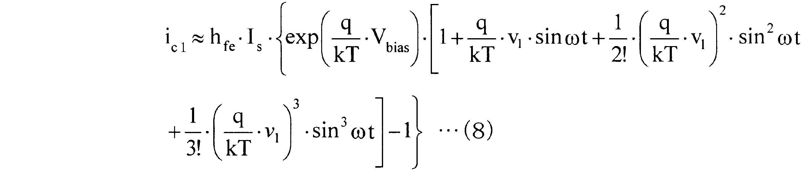
- the collector current ic1 of the transistor 15 can be expressed by equation (8).
- Equation (9) is obtained by integrating Equation (8).
- reference numeral 1 denotes the emitter terminals of the transistors 15 and 16
- reference numeral 2 denotes the base terminal of the transistor
- reference numeral 3 denotes the base terminal of the transistor 16
- reference numeral 4 denotes the power supply line 14.
- the noise voltage is defined by equation (11).
- the voltage amplitude between the base and emitter of the transistor 15 can be expressed by equation (12).
- Equation (2) Substituting Equations (13) and (14) into Equation (10) yields Equation (2).
- the impedances between the collectors of the transistors 15 and 16 and the power supply line 14 are dominated by the impedances 1 / (j ⁇ Cp) and 1 / (j ⁇ Cm) of the capacitors 21 and 22.
- the capacitance values Cp and Cm are made equal, the impedance balance between the collectors of the transistors 15 and 16 and the power supply line 14 can be improved, and the DC displacement of the output voltage Vo can be suppressed.
- the capacitance values Cp and Cm are determined so as to obtain a predetermined balance. For example, when the noise frequency is 100 MHz or more, the parasitic capacitances of the transistors 15 and 16 are about several tens of fF, so the capacitance values Cp and Cm may be set to about several tens of pF.
- the differential amplifier 11 of this embodiment includes the capacitors 21 and 22 between the collectors of the transistors 15 and 16 and the power supply line 14.
- the impedance between the collectors of the transistors 15 and 16 and the power supply line 14 can be made close to each other and balanced. As a result, it is possible to reduce the DC displacement that appears in the output voltage Vo.
- noise that has entered from the output terminal of the differential amplifier 11 is bypassed to the power supply line 14 via the capacitor 22, noise added between the base and emitter of the transistor 25 of the output amplifier circuit 23 is reduced. Thereby, even when noise enters from the output terminal, the direct current displacement due to the nonlinearity of the transistor 25 can be suppressed, and the immunity resistance against the noise can be maintained high.
- the impedance between the collectors of the transistors 15 and 16 and the power supply line 14 may be balanced.
- the capacitance values of the capacitors 21 and 22 are preferably set so that the impedance between the collector of the transistor 15 and the power supply line 14 and the impedance between the collector of the transistor 16 and the power supply line 14 are equal to each other. .
- the capacitance values Cp and Cm of the capacitors 21 and 22 are determined so that the phase margin is secured to a predetermined value or more necessary for stable operation.
- a configuration using a FET such as a MOS transistor instead of the bipolar transistor may be used.
- the configurations of the constant current circuit 17, the active load 20, and the output amplifier circuit 23 are not limited to the illustrated configurations, and can be variously changed as long as the same operation is achieved.
- the first and second differential input transistors are composed of NPN transistors (N-channel type if FET), the constant current circuit 17 is disposed on the power supply line 14 side, and the active load 20 is disposed on the power supply line 13 side. It is good also as a structure. In this case, direct current displacement due to noise entering the power supply line 13 can be prevented.
Landscapes
- Engineering & Computer Science (AREA)
- Power Engineering (AREA)
- Amplifiers (AREA)
Abstract
作動増幅器において、トランジスタ(15、16)の各コレクタと電源線(14)との間にキャパシタ(21、22)を備えることにより、トランジスタ(15、16)の各コレクタと電源線(14)との間のインピーダンスを互いに接近した値にして平衡させる。電源線(14)にノイズが侵入したとき、トランジスタ(15、16)のコレクタに加わるノイズの振幅がほぼ等しくなり、寄生容量を介したベース・エミッタ間電圧もほぼ等しくなる。その結果、トランジスタ(15、16)の非線形特性により流れる直流変位電流が相殺されて、出力電圧Voの直流変位が抑制される。
Description
本開示は、2013年6月17日に出願された日本出願番号2013-126584号に基づくもので、ここにその記載内容を援用する。
本開示は、差動対と出力増幅回路とを備えた差動増幅器に関する。
車両に搭載された電子制御装置は、センサに対し電源線を通して電源電圧を供給するとともに、センサから信号線を通して伝送されてくるセンサ信号を入力する。電子制御装置が備える差動増幅器は、微小なセンサ信号を増幅してA/D変換器に出力する。電源線および信号線には誘導ノイズが侵入し易い。そこで、差動増幅器のイミュニティ対策として、例えば高電位側電源線および差動増幅器の入力部に抵抗とキャパシタからなるフィルタが付加される(特許文献1)。この構成は、高電位側電源端子および信号入力端子を介したノイズの侵入に対して有効である。
上述したフィルタは、能動負荷が接続される低電位側電源線(グランド線)を介したノイズの侵入に対しては機能しない。実際のノイズ試験で、グランド線にノイズを注入したところ、差動増幅器の出力電圧に直流変位が発生した。この現象は、差動対の片側ノードから出力増幅回路に信号を取り出す構成で顕著になる。
本開示は上記事情に鑑みてなされたもので、その目的は、能動負荷が接続される側の電源線を介してノイズが侵入したときの出力電圧の直流変位を抑制可能な差動増幅器を提供することにある。
本開示の第一の態様によれば、差動増幅器は、差動対を構成する第1、第2差動入力トランジスタ、定電流回路、能動負荷および出力増幅回路に加え、第1キャパシタと第2キャパシタのうち少なくとも一方のキャパシタを備えている。差動増幅器は、第1電源線と第2電源線との間に与えられる電源電圧により動作する。
第1、第2差動入力トランジスタは、制御端子(ベース、ゲート)と第1通電端子(エミッタ、ソース)との間に差動信号が入力され、第1通電端子が互いに接続されている。定電流回路は、第1電源線と第1、第2差動入力トランジスタの第1通電端子との間に設けられている。能動負荷は、第1、第2差動入力トランジスタの第2通電端子(コレクタ、ドレイン)と第2電源線との間に設けられている。出力増幅回路は、能動負荷に生じる電圧を増幅して出力する。
第1、第2キャパシタを備えない構成では、第2電源線を介して交流ノイズが侵入すると、差動増幅器の出力電圧に直流変位が発生する。この原因は、以下の作用によるものと考えられる。第1、第2差動入力トランジスタの第2通電端子と第2電源線との間のノイズの周波数範囲におけるインピーダンスは、能動負荷および出力増幅回路の構成に応じて互いに異なる(不平衡)。
インピーダンスが不平衡であると、第2電源線にノイズが侵入したときに、第1、第2差動入力トランジスタの第2通電端子に加わるノイズの振幅に差が生じる。この振幅差は、第1、第2差動入力トランジスタの寄生容量を通して、制御端子と第1通電端子との間の制御電圧の振幅差となって現れるので、ノイズにより第1、第2差動入力トランジスタに流れる電流に差が生じる。
さらに、第1、第2差動入力トランジスタの制御電圧と電流との関係は、線形な関係ではなく、トランジスタ素子の静特性から定まる非線形性を有している。このため、制御端子と第1通電端子との間に交流ノイズが印加されると、そのときの動作点に対し差動入力トランジスタに流れる電流の増加幅と減少幅とが相違する。その結果、差動入力トランジスタに流れる電流の直流分(平均値)が変位する。
第1、第2差動入力トランジスタに印加される交流ノイズの振幅が等しいときには、上記直流変位電流は相殺される。しかし、印加される交流ノイズに振幅差があると、第1、第2差動入力トランジスタに上記直流変位電流の差分電流が流れ、出力増幅回路を介して出力電圧に直流変位を発生させる。
そこで、上記構成では、第1差動入力トランジスタの第2通電端子と第2電源線との間に接続される第1キャパシタおよび第2差動入力トランジスタの第2通電端子と第2電源線との間に接続される第2キャパシタのうち少なくとも一方のキャパシタを備えている。これにより、第1差動入力トランジスタの第2通電端子と第2電源線との間のインピーダンスと、第2差動入力トランジスタの第2通電端子と第2電源線との間のインピーダンスとを、互いに接近した値としている。
この場合の第1キャパシタおよび/または第2キャパシタの容量値は、第2電源線に侵入するノイズの周波数範囲において、当該ノイズによる出力増幅回路の出力電圧の直流変位が抑制されるように設定されている。この構成によれば、第2電源線にノイズが侵入したときの出力電圧の直流変位を抑制できる。
さらに、差動増幅器の出力端子から侵入したノイズが、位相補償キャパシタ等を介して出力増幅回路の入力側に印加されたときも、出力増幅回路が有する非線形性により、出力電圧に直流変位を発生させる。差動対のうち出力増幅回路が接続される側に上記第1または第2キャパシタが接続される構成では、そのキャパシタが、差動増幅器の出力端子から侵入するノイズを第2電源線にバイパスさせる。そのため、出力端子からノイズが侵入したときの出力電圧変動も抑制できる。
本開示の第二の態様によれば、第1、第2差動入力トランジスタの第2通電端子と第2電源線との間のインピーダンスが、第2電源線に侵入するノイズの周波数に対応して予め定められた周波数範囲において所定の平衡度を満たすように、第1キャパシタおよび/または第2キャパシタの容量値が設定されている。これにより、当該予め定められた周波数範囲において平衡度が改善され、第1、第2差動入力トランジスタに生じる直流変位電流が相殺される。その結果、第2電源線にノイズが侵入したときの出力電圧の直流変位を抑制できる。
本開示の第三の態様によれば、第1、第2キャパシタの容量値は互いに等しく設定されている。このような第1、第2キャパシタを設けると、第1、第2差動入力トランジスタの第2通電端子と第2電源線との間のインピーダンスの平衡度が改善される。この効果は、ノイズの周波数範囲において、第1、第2差動入力トランジスタの第2通電端子と第2電源線との間のインピーダンスに比べ、付加する第1、第2キャパシタのインピーダンスが小さいほど高くなる。
本開示の第四の態様によれば、第1、第2差動入力トランジスタの第2通電端子と第2電源線との間のインピーダンスが互いに等しくなるように、第1キャパシタおよび/または第2キャパシタの容量値が設定されている。この構成によれば、第1、第2差動入力トランジスタに印加される交流ノイズの振幅が等しくなるので、直流変位電流が相殺されて出力電圧の直流変位を防止できる。
本開示についての上記目的およびその他の目的、特徴や利点は、添付の図面を参照しながら下記の詳細な記述により、より明確になる。図面において、
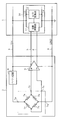
一実施形態を示す差動増幅器の概略構成図
差動増幅器の回路図
電子制御装置とセンサ装置の概略構成図
トランジスタのVBE-Ic特性を示す図
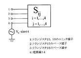
ノイズ源からトランジスタのベース端子、エミッタ端子への伝搬特性を示す図
本開示に係る差動増幅器を、車両の電子制御装置に搭載された半導体集積回路装置(IC)に適用した一実施形態について図面を参照しながら説明する。電子制御装置1は、図3に示すようにセンサ装置(ここでは圧力センサ2)に対し電源線3、4を介して電源電圧Vccを供給し、圧力センサ2から信号線5、6を介して差動形式のセンサ信号を入力する。電源線3、4および信号線5、6は、車両内に配設されるワイヤハーネスである。
圧力センサ2は、基板に組み立てられ、或いはモジュール化されている。圧力センサ2は、ダイアフラム上にホイートストンブリッジを構成するように形成されたピエゾ抵抗素子7a~7dを備えている。バイアス回路8は、ホイートストンブリッジの端子7p、7qを介して一定の駆動電流を流す。これにより、端子7r、7s間に圧力に応じた電圧が生じる。バッファ回路9は、そのセンサ信号を差動形式で信号線5、6に出力する。
電子制御装置1は、IC10を備えている。IC10は、上記差動信号形式のセンサ信号を増幅する差動増幅器11と、増幅されたセンサ信号をA/D変換するA/D変換器12を備えている。IC10に形成された各回路は、IC内部に配された第1電源線13と第2電源線14を介して与えられる電源電圧Vccにより動作する。電源線13、14は、上述した電源線3、4と接続されている。
図1および図2に示すように、差動増幅器11は、差動対を構成するPNP形の第1、第2差動入力トランジスタ15、16を備えている。トランジスタ15、16のベース、エミッタ、コレクタは、それぞれ制御端子、第1通電端子、第2通電端子に相当する。電源線13とトランジスタ15、16のエミッタとの間には、定電流回路17が共通に設けられている。
トランジスタ15、16のコレクタと電源線14との間には、NPN形のトランジスタ18、19からなる能動負荷20が設けられている。トランジスタ18、19のエミッタは、電源線14に接続されている。トランジスタ18、19のコレクタは、それぞれトランジスタ15、16のコレクタ(ノードNa、Nb)に接続されている。トランジスタ18のベースとコレクタは接続されている。
トランジスタ15、16のコレクタと電源線14との間には、それぞれ第1、第2キャパシタ21、22が設けられている。ノードNbは差動対の出力ノードである。出力増幅回路23は、能動負荷20に生じるノードNbの電圧を増幅した電圧Voを出力する。出力増幅回路23は、電源線13と出力ノードNcとの間に接続された定電流回路24、出力ノードNcと電源線14との間に接続されたNPN形トランジスタ25、およびノードNb、Nc間に接続された位相補償用のキャパシタ26から構成されている。トランジスタ25のベースは、ノードNbに接続されている。
次に、本実施形態の作用について図4および図5も参照しながら説明する。車両に配設された電源線3、4および信号線5、6からなるワイヤハーネスは、シールド等によってノイズ対策が施されている。しかし、外部からの誘導ノイズを完全に遮断することは難しい。ここでは、主として電源線4に交流ノイズ(以下、単にノイズと言う)が侵入する場合について説明する。
ノイズは、ワイヤハーネスを通してプリント基板内の電源線14に侵入する。本実施形態で問題となるノイズの周波数は、トランジスタ15、16の寄生容量CBCを通してノイズが伝搬する程度の高い周波数(一例として100MHz以上の周波数)である。本発明者が実施したノイズ試験の結果、キャパシタ21、22が付加されていない従来の差動増幅器では、電源線14にノイズが侵入すると、差動増幅器の出力電圧Voに直流変位が生じることが分かった。
そこで、本発明者は、回路解析および回路シミュレーションを行って、出力電圧Voに直流変位が生じる作用を以下のように解明した。すなわち、キャパシタ21、22が付加されていない従来の差動増幅器では、トランジスタ15、16の各コレクタ(ノードNa、Nb)と電源線14との間のノイズの周波数範囲におけるインピーダンスは互いに異なる(不平衡)。トランジスタ15のコレクタには能動負荷20だけが接続されているが、トランジスタ16のコレクタには能動負荷20に加え、出力増幅回路23も接続されているからである。
トランジスタ15、16の各コレクタと電源線14との間のインピーダンスが不平衡であると、電源線14にノイズが侵入したときに、トランジスタ15、16のコレクタに加わるノイズの振幅に差が生じる。トランジスタ15、16のコレクタに伝搬されたノイズは、トランジスタ15、16のベース・コレクタ間の寄生容量CBCを介して、ベース・エミッタ間に印加される。つまり、コレクタ電位の振幅差は、ベース・エミッタ間電圧VBEの差となって現れる。
一般に、トランジスタのベース・エミッタ間電圧VBEとコレクタ電流Icとの関係は、図4に示すように指数関数特性を持つ非線形特性となる。動作点Mに対しベース・エミッタ間に正弦波状のノイズが加わると、動作点Mからのコレクタ電流Icの増加幅が、動作点Mからのコレクタ電流Icの減少幅よりも大きくなる。その結果、ノイズの侵入により、トランジスタのコレクタ電流の直流分(平均値)がΔIだけ増加する。
トランジスタ15、16のベース・エミッタ間に加わるノイズの振幅が等しいときには、上記変位電流ΔIは互いに打ち消しあう。しかし、上述したインピーダンスの不平衡によりベース・エミッタ間電圧VBEに差が生じると、トランジスタ15、16に直流変位電流の差分電流が流れる。その結果、見かけ上の動作点Mがずれて、ノードNbの電圧の直流分(平均値)も変位する。出力増幅回路23はこの変位電圧を増幅するので、出力電圧Voにも直流変位が生じる。
図2に示す差動増幅器11からキャパシタ21、22を除いた従来構成では、トランジスタ15、16のコレクタと電源線14との間のインピーダンスをそれぞれZp、Zmとすれば、Zp>Zmの不平衡となっている。このため、ベース・エミッタ間に伝搬されるノイズ電圧は、トランジスタ15よりもトランジスタ16の方が大きくなる。その結果、動作点Mに対してトランジスタ16のコレクタ電流Ic(直流分)が増加し、ノードNbの電圧が上昇し、出力電圧Voが低下する。
差動増幅器11の出力端子から侵入したノイズが、キャパシタ26等を介して出力増幅回路23の入力側に印加されたときも、出力増幅回路23が有する非線形性により、出力電圧に直流変位を発生させる。
この解明した作用によれば、ノイズの周波数範囲において、トランジスタ15、16の各コレクタと電源線14との間のインピーダンスを互いに接近した値にして平衡させれば、出力電圧Voの直流変位を低減できることが分かる。そこで、差動増幅器11では、ノードNa、Nbと電源線14との間にそれぞれキャパシタ21、22を備えることにより、両インピーダンスを平衡させている。
キャパシタ21、22の容量値をそれぞれCp、Cmとすれば、平衡条件は(1)式となる。左辺は、トランジスタ15のコレクタと電源線14との間のインピーダンスである。右辺は、トランジスタ16のコレクタと電源線14との間のインピーダンスである。両辺の値が完全に等しくない場合でも、両辺の値が互いに接近した値であれば、ノイズの周波数範囲においてノイズによる出力電圧Voの直流変位が抑制される。

トランジスタ15、16の各コレクタと電源線14との間のインピーダンスが、直流変位抑制効果が得られる平衡度(所定の平衡度)となるように、容量値Cp、Cmは、以下に説明する第1から第3の何れかの方法により決定される。
[第1の方法]
出力電圧Voの直流変位の制限値から理論的に容量値Cp、Cmを導出する。ここでは、出力電圧Voの直流変位電圧をΔVo以下に制限することを要件とする。この要件を満たすためには、出力増幅回路23の入力電圧の直流変位電圧をΔVo′以下にし、トランジスタ16のコレクタ電流の直流変位をΔIo以下に制限する必要がある。これらΔVo′、ΔIoの値は、回路特性から導き出すことができる。
出力電圧Voの直流変位の制限値から理論的に容量値Cp、Cmを導出する。ここでは、出力電圧Voの直流変位電圧をΔVo以下に制限することを要件とする。この要件を満たすためには、出力増幅回路23の入力電圧の直流変位電圧をΔVo′以下にし、トランジスタ16のコレクタ電流の直流変位をΔIo以下に制限する必要がある。これらΔVo′、ΔIoの値は、回路特性から導き出すことができる。
電源線14にノイズが侵入したとき、トランジスタ16のコレクタ電流の直流変位電流ΔIは、(2)式で表すことができる。

ここで、Vbiasはノイズが侵入していないときのトランジスタ16のベース・エミッタ間電圧を表し、Vnはノイズの振幅を表す。hfeは電流増幅率、Isは飽和電流、qは電子の電荷、kはボルツマン定数、Tは絶対温度である。S41、S42、S43は、図5に示すように、電源線14からトランジスタ15、16のエミッタ端子、ベース端子への伝播特性を表すSパラメータである。
所定の平衡度を満たすためには、(3)式を満たすように容量値Cp、Cmを決定すればよい。

は、ノイズの振幅である。







[第2の方法]
シミュレーションにより適切な容量値を探索し、決定する。すなわち、差動増幅器11において、電源線14に対してノイズを注入するシミュレーションを実施する。シミュレーションにおいて、差動増幅器11の出力電圧Voの直流変位電圧が所望の値以下になるように、キャパシタ21、22の容量値Cp、Cmを変化させる。その結果、所定の平衡度が満たされたとき、差動増幅器11の出力電圧Voの直流変位電圧が所望の値以下になる。
シミュレーションにより適切な容量値を探索し、決定する。すなわち、差動増幅器11において、電源線14に対してノイズを注入するシミュレーションを実施する。シミュレーションにおいて、差動増幅器11の出力電圧Voの直流変位電圧が所望の値以下になるように、キャパシタ21、22の容量値Cp、Cmを変化させる。その結果、所定の平衡度が満たされたとき、差動増幅器11の出力電圧Voの直流変位電圧が所望の値以下になる。
[第3の方法]
(15)式、(16)式に示すように、トランジスタ15、16その他の素子の寄生容量を無視できる十分に大きい容量値Cp、Cmを持つキャパシタ21、22を接続する。
(15)式、(16)式に示すように、トランジスタ15、16その他の素子の寄生容量を無視できる十分に大きい容量値Cp、Cmを持つキャパシタ21、22を接続する。

この効果は、ノイズの周波数範囲において、トランジスタ15、16の各コレクタと電源線14との間のインピーダンスZp、Zm(キャパシタ21、22のインピーダンスを除く)に比べ、キャパシタ21、22のインピーダンスが小さいほど高くなる。所定の平衡度が得られるように容量値Cp、Cmを決定する。例えば、ノイズ周波数が100MHz以上の場合、トランジスタ15、16の寄生容量は数十fF程度であるため、容量値Cp、Cmを十数pF程度に設定すればよい。
以上説明したように、本実施形態の差動増幅器11は、トランジスタ15、16の各コレクタと電源線14との間にキャパシタ21、22を備えている。これにより、電源線14に侵入するノイズの周波数範囲において、トランジスタ15、16の各コレクタと電源線14との間のインピーダンスを互いに接近した値にして平衡させることができる。その結果、出力電圧Voに現れる直流変位を低減することができる。
差動増幅器11の出力端子から侵入したノイズは、キャパシタ22を介して電源線14にバイパスされるので、出力増幅回路23のトランジスタ25のベース・エミッタ間に加わるノイズが低減する。これにより、出力端子からノイズが侵入した場合でも、トランジスタ25の非線形性による直流電流変位を抑制することができ、当該ノイズに対するイミュニティ耐量を高く維持することができる。
以上、本開示の好適な実施形態について説明したが、本開示は上述した実施形態に限定されるものではなく、開示の要旨を逸脱しない範囲内で種々の変形、拡張を行うことができる。
キャパシタ21、22の何れか一方だけを備えることにより、トランジスタ15、16の各コレクタと電源線14との間のインピーダンスを平衡させてもよい。
トランジスタ15のコレクタと電源線14との間のインピーダンスと、トランジスタ16のコレクタと電源線14との間のインピーダンスが互いに等しくなるように、キャパシタ21、22の容量値が設定されていることが好ましい。
キャパシタ21、22の容量値Cp、Cmは、位相余裕が安定動作のために必要な規定値以上確保されるように決定することが好ましい。
バイポーラトランジスタに替えてMOSトランジスタなどのFETを用いた構成であってもよい。定電流回路17、能動負荷20および出力増幅回路23の構成は、図示した構成に限られず、同様の作用を奏する限りにおいて種々に変更できる。第1、第2差動入力トランジスタをNPN形トランジスタ(FETであればNチャネル型)で構成し、電源線14側に定電流回路17を配置し、電源線13側に能動負荷20を配置する構成としてもよい。この場合には、電源線13に侵入するノイズによる直流変位を防止できる。
Claims (4)
- 制御端子、第1通電端子、第2通電端子をそれぞれ有し、前記制御端子と前記第1通電端子との間に差動信号が入力され、前記第1通電端子が互いに接続された第1、第2差動入力トランジスタ(15,16)と、
第1電源線(13)と前記第1、第2差動入力トランジスタの第1通電端子との間に設けられた定電流回路(17)と、
前記第1、第2差動入力トランジスタの第2通電端子と第2電源線(14)との間に設けられた能動負荷(20)と、
前記能動負荷に生じる電圧を増幅して出力する出力増幅回路(23)と、
前記第1差動入力トランジスタの第2通電端子と前記第2電源線との間に接続される第1キャパシタ(21)および前記第2差動入力トランジスタの第2通電端子と前記第2電源線との間に接続される第2キャパシタ(22)のうち少なくとも一方のキャパシタとを備え、
前記第1差動入力トランジスタの第2通電端子と前記第2電源線との間のインピーダンスおよび前記第2差動入力トランジスタの第2通電端子と前記第2電源線との間のインピーダンスが互いに接近した値になることにより、前記第2電源線に侵入するノイズの周波数範囲において当該ノイズによる前記出力増幅回路の出力電圧の直流変位が抑制されるように、前記少なくとも一方のキャパシタの容量値が設定されている差動増幅器。 - 前記第1差動入力トランジスタの第2通電端子と前記第2電源線との間のインピーダンスおよび前記第2差動入力トランジスタの第2通電端子と前記第2電源線との間のインピーダンスが、前記第2電源線に侵入するノイズの周波数に対応して予め定められた周波数範囲において所定の平衡度を満たすように、前記少なくとも一方のキャパシタの容量値が設定されている請求項1記載の差動増幅器。
- 前記第1、第2キャパシタの容量値は互いに等しく設定されている請求項1または2記載の差動増幅器。
- 前記第1差動入力トランジスタの第2通電端子と前記第2電源線との間のインピーダンスと、前記第2差動入力トランジスタの第2通電端子と前記第2電源線との間のインピーダンスが互いに等しくなるように、前記少なくとも一方のキャパシタの容量値が設定されている請求項1または2記載の差動増幅器。
Applications Claiming Priority (2)
| Application Number | Priority Date | Filing Date | Title |
|---|---|---|---|
| JP2013126584A JP2015002457A (ja) | 2013-06-17 | 2013-06-17 | 差動増幅器 |
| JP2013-126584 | 2013-06-17 |
Publications (1)
| Publication Number | Publication Date |
|---|---|
| WO2014203473A1 true WO2014203473A1 (ja) | 2014-12-24 |
Family
ID=52104225
Family Applications (1)
| Application Number | Title | Priority Date | Filing Date |
|---|---|---|---|
| PCT/JP2014/002919 Ceased WO2014203473A1 (ja) | 2013-06-17 | 2014-06-03 | 差動増幅器 |
Country Status (2)
| Country | Link |
|---|---|
| JP (1) | JP2015002457A (ja) |
| WO (1) | WO2014203473A1 (ja) |
Citations (8)
| Publication number | Priority date | Publication date | Assignee | Title |
|---|---|---|---|---|
| JPH06260855A (ja) * | 1993-03-08 | 1994-09-16 | Nec Ic Microcomput Syst Ltd | 多段直結増幅回路 |
| JPH08204468A (ja) * | 1995-01-20 | 1996-08-09 | Seikosha Co Ltd | 演算増幅器 |
| JPH08274259A (ja) * | 1995-03-29 | 1996-10-18 | Nissan Motor Co Ltd | 演算増幅器回路 |
| JP2000049546A (ja) * | 1998-07-28 | 2000-02-18 | Mitsubishi Electric Corp | オフセット調整装置 |
| WO2002052737A1 (en) * | 2000-12-22 | 2002-07-04 | Niigata Seimitsu Co., Ltd. | Limit circuit |
| JP2008306562A (ja) * | 2007-06-08 | 2008-12-18 | Asahi Kasei Electronics Co Ltd | 演算増幅器 |
| JP2009171350A (ja) * | 2008-01-17 | 2009-07-30 | Nsc Co Ltd | ラジオ受信機およびこれに用いる受信用半導体集積回路 |
| JP2012204860A (ja) * | 2011-03-23 | 2012-10-22 | Toshiba Corp | 半導体集積回路および受信装置 |
-
2013
- 2013-06-17 JP JP2013126584A patent/JP2015002457A/ja active Pending
-
2014
- 2014-06-03 WO PCT/JP2014/002919 patent/WO2014203473A1/ja not_active Ceased
Patent Citations (8)
| Publication number | Priority date | Publication date | Assignee | Title |
|---|---|---|---|---|
| JPH06260855A (ja) * | 1993-03-08 | 1994-09-16 | Nec Ic Microcomput Syst Ltd | 多段直結増幅回路 |
| JPH08204468A (ja) * | 1995-01-20 | 1996-08-09 | Seikosha Co Ltd | 演算増幅器 |
| JPH08274259A (ja) * | 1995-03-29 | 1996-10-18 | Nissan Motor Co Ltd | 演算増幅器回路 |
| JP2000049546A (ja) * | 1998-07-28 | 2000-02-18 | Mitsubishi Electric Corp | オフセット調整装置 |
| WO2002052737A1 (en) * | 2000-12-22 | 2002-07-04 | Niigata Seimitsu Co., Ltd. | Limit circuit |
| JP2008306562A (ja) * | 2007-06-08 | 2008-12-18 | Asahi Kasei Electronics Co Ltd | 演算増幅器 |
| JP2009171350A (ja) * | 2008-01-17 | 2009-07-30 | Nsc Co Ltd | ラジオ受信機およびこれに用いる受信用半導体集積回路 |
| JP2012204860A (ja) * | 2011-03-23 | 2012-10-22 | Toshiba Corp | 半導体集積回路および受信装置 |
Also Published As
| Publication number | Publication date |
|---|---|
| JP2015002457A (ja) | 2015-01-05 |
Similar Documents
| Publication | Publication Date | Title |
|---|---|---|
| JP2001223546A (ja) | 多段信号増幅回路 | |
| CN105556834A (zh) | 放大电路 | |
| KR101834255B1 (ko) | 영상신호 출력 회로 | |
| JP4573602B2 (ja) | 増幅装置 | |
| US8624671B2 (en) | Audio amplifying circuit with improved noise performance | |
| US11199564B2 (en) | Current sensing circuit | |
| US11101776B2 (en) | Common source preamplifier for a MEMS capacitive sensor | |
| US6734720B2 (en) | Operational amplifier in which the idle current of its output push-pull transistors is substantially zero | |
| US8803493B2 (en) | Voltage regulator with differentiating and amplifier circuitry | |
| WO2014203473A1 (ja) | 差動増幅器 | |
| JP2000022451A (ja) | 信号処理回路装置 | |
| JP2006319388A (ja) | 自動利得制御回路及びそれを用いた正弦波発振回路 | |
| JP5388670B2 (ja) | センサ信号処理回路 | |
| JP4360267B2 (ja) | 増幅回路 | |
| RU2292636C1 (ru) | Дифференциальный усилитель с повышенным ослаблением синфазного сигнала | |
| JP2006033091A (ja) | センサユニット及びセンサ信号処理回路 | |
| JP6933797B2 (ja) | オーディオアンプおよびオーディオパワーアンプ | |
| JP2021010048A (ja) | 演算増幅器 | |
| US10461706B1 (en) | Differential amplifier including cancellation capacitors | |
| JP5060890B2 (ja) | 半導体装置 | |
| Litovski | 4 Discrete and Integrated Power Amplifier Circuits | |
| JP2016086230A (ja) | センサ装置 | |
| TWI508434B (zh) | 放大器電路及放大訊號方法 | |
| US9093992B1 (en) | Current-boosting output stage with short-circuit protection | |
| JP5350882B2 (ja) | 容量増倍回路 |
Legal Events
| Date | Code | Title | Description |
|---|---|---|---|
| 121 | Ep: the epo has been informed by wipo that ep was designated in this application |
Ref document number: 14812934 Country of ref document: EP Kind code of ref document: A1 |
|
| NENP | Non-entry into the national phase |
Ref country code: DE |
|
| 122 | Ep: pct application non-entry in european phase |
Ref document number: 14812934 Country of ref document: EP Kind code of ref document: A1 |