WO2014199672A1 - 半導体素子、および半導体素子の製造方法 - Google Patents
半導体素子、および半導体素子の製造方法 Download PDFInfo
- Publication number
- WO2014199672A1 WO2014199672A1 PCT/JP2014/055029 JP2014055029W WO2014199672A1 WO 2014199672 A1 WO2014199672 A1 WO 2014199672A1 JP 2014055029 W JP2014055029 W JP 2014055029W WO 2014199672 A1 WO2014199672 A1 WO 2014199672A1
- Authority
- WO
- WIPO (PCT)
- Prior art keywords
- layer
- gate insulating
- electrode
- insulating layer
- drain electrode
- Prior art date
- Legal status (The legal status is an assumption and is not a legal conclusion. Google has not performed a legal analysis and makes no representation as to the accuracy of the status listed.)
- Ceased
Links
Images







Classifications
-
- H—ELECTRICITY
- H10—SEMICONDUCTOR DEVICES; ELECTRIC SOLID-STATE DEVICES NOT OTHERWISE PROVIDED FOR
- H10K—ORGANIC ELECTRIC SOLID-STATE DEVICES
- H10K10/00—Organic devices specially adapted for rectifying, amplifying, oscillating or switching; Organic capacitors or resistors having potential barriers
- H10K10/40—Organic transistors
- H10K10/46—Field-effect transistors, e.g. organic thin-film transistors [OTFT]
- H10K10/462—Insulated gate field-effect transistors [IGFETs]
- H10K10/466—Lateral bottom-gate IGFETs comprising only a single gate
-
- H—ELECTRICITY
- H10—SEMICONDUCTOR DEVICES; ELECTRIC SOLID-STATE DEVICES NOT OTHERWISE PROVIDED FOR
- H10K—ORGANIC ELECTRIC SOLID-STATE DEVICES
- H10K10/00—Organic devices specially adapted for rectifying, amplifying, oscillating or switching; Organic capacitors or resistors having potential barriers
- H10K10/40—Organic transistors
- H10K10/46—Field-effect transistors, e.g. organic thin-film transistors [OTFT]
- H10K10/462—Insulated gate field-effect transistors [IGFETs]
- H10K10/468—Insulated gate field-effect transistors [IGFETs] characterised by the gate dielectrics
- H10K10/474—Insulated gate field-effect transistors [IGFETs] characterised by the gate dielectrics the gate dielectric comprising a multilayered structure
-
- H—ELECTRICITY
- H10—SEMICONDUCTOR DEVICES; ELECTRIC SOLID-STATE DEVICES NOT OTHERWISE PROVIDED FOR
- H10K—ORGANIC ELECTRIC SOLID-STATE DEVICES
- H10K10/00—Organic devices specially adapted for rectifying, amplifying, oscillating or switching; Organic capacitors or resistors having potential barriers
- H10K10/40—Organic transistors
- H10K10/46—Field-effect transistors, e.g. organic thin-film transistors [OTFT]
- H10K10/462—Insulated gate field-effect transistors [IGFETs]
- H10K10/481—Insulated gate field-effect transistors [IGFETs] characterised by the gate conductors
-
- H—ELECTRICITY
- H10—SEMICONDUCTOR DEVICES; ELECTRIC SOLID-STATE DEVICES NOT OTHERWISE PROVIDED FOR
- H10K—ORGANIC ELECTRIC SOLID-STATE DEVICES
- H10K10/00—Organic devices specially adapted for rectifying, amplifying, oscillating or switching; Organic capacitors or resistors having potential barriers
- H10K10/80—Constructional details
- H10K10/82—Electrodes
- H10K10/84—Ohmic electrodes, e.g. source or drain electrodes
-
- H—ELECTRICITY
- H10—SEMICONDUCTOR DEVICES; ELECTRIC SOLID-STATE DEVICES NOT OTHERWISE PROVIDED FOR
- H10K—ORGANIC ELECTRIC SOLID-STATE DEVICES
- H10K71/00—Manufacture or treatment specially adapted for the organic devices covered by this subclass
- H10K71/10—Deposition of organic active material
- H10K71/12—Deposition of organic active material using liquid deposition, e.g. spin coating
- H10K71/13—Deposition of organic active material using liquid deposition, e.g. spin coating using printing techniques, e.g. ink-jet printing or screen printing
- H10K71/135—Deposition of organic active material using liquid deposition, e.g. spin coating using printing techniques, e.g. ink-jet printing or screen printing using ink-jet printing
-
- H—ELECTRICITY
- H10—SEMICONDUCTOR DEVICES; ELECTRIC SOLID-STATE DEVICES NOT OTHERWISE PROVIDED FOR
- H10K—ORGANIC ELECTRIC SOLID-STATE DEVICES
- H10K71/00—Manufacture or treatment specially adapted for the organic devices covered by this subclass
- H10K71/60—Forming conductive regions or layers, e.g. electrodes
Definitions
- the present invention relates to a semiconductor element and a method for manufacturing the semiconductor element.
- TFT Thin Film Transistor
- the organic TFT can be manufactured by a low temperature process of about 100 ° C. to 200 ° C., it can be directly formed on a plastic substrate.
- both the semiconductor layer and the insulating layer are formed of an organic material, the organic TFT has high resistance to bending, and is expected to be applied to flexible displays such as film liquid crystal and electronic paper.
- a bottom gate / bottom contact structure As a general structure of the organic TFT, a bottom gate / bottom contact structure is widely applied.
- a gate electrode and a gate insulating layer are formed on a substrate, and then a source electrode and a drain electrode are formed on the gate insulating layer. Thereafter, an organic semiconductor is formed on the gate insulating layer, the source electrode, and the drain electrode.
- gold which is a metal that can make good contact with the organic semiconductor layer
- the source electrode and the drain electrode are Au (gold).
- it is formed as a single layer film.
- an organic semiconductor channel is formed in a region near the interface between the organic semiconductor layer and the gate insulating layer, which is located between the source electrode and the drain electrode. It can flow inside.
- a gate insulating layer is further provided between a source electrode and a drain electrode to form a planarization layer that planarizes the organic semiconductor layer, thereby improving mobility of carriers that move through the channel of the organic semiconductor.
- Non-Patent Document 1 discloses a configuration in which an adhesion layer is further provided in an organic transistor having a bottom gate structure.
- the adhesion layer is an auxiliary metal layer provided on the gate electrode, the source electrode, and the drain electrode in order to improve adhesion between each electrode and the base (substrate and gate insulating layer).
- Patent Documents 1 and 2 have the following problems.
- the source electrode and the drain electrode are composed of a plurality of layers. That is, in order to improve the adhesion between each electrode and the base (substrate and gate insulating layer), the gate electrode, the source electrode, and the drain electrode have Ti (titanium) or Cr as the first layer (adhesion layer). A metal layer formed of (chrome) or the like is provided below a second layer (contact layer) formed of Au (gold) or the like.
- the contact resistance in the organic semiconductor increases due to the presence of the adhesion layer. Therefore, the current flowing in the channel of the organic semiconductor is reduced, causing a problem that the characteristics of the organic TFT are deteriorated.
- the source electrode and the drain electrode are formed as a single-layer metal film, and the structure of the organic transistor disclosed in Patent Document 1 is a bottom gate in the research stage.
- the structure is the same as the general structure of the organic TFT.
- Patent Documents 1 and 2 have a problem that it is impossible to cope with the deterioration in characteristics that occurs in the semiconductor element in which the source electrode and the drain electrode are composed of a plurality of layers.
- the present invention has been made in order to solve the above-described problem, and an object of the present invention is to provide a semiconductor element capable of suppressing deterioration in characteristics that occurs in a semiconductor element in which a source electrode and a drain electrode are composed of a plurality of layers. And to provide a method of manufacturing such a semiconductor device.
- a semiconductor element includes a gate electrode, a first gate insulating layer that covers the gate electrode, and the gate in a plan view over the first gate insulating layer.
- a source electrode and a drain electrode that are spaced apart from each other with an electrode interposed therebetween and overlap with a part of the gate electrode via the first gate insulating layer, and at least the source electrode on the first gate insulating layer
- a second gate insulating layer formed in a region sandwiched by the drain electrode; and the first gate insulating layer and the second gate formed between the source electrode and the drain electrode and on the source electrode and the drain electrode.
- a semiconductor layer overlapping with the gate electrode through an insulating layer, a source electrode, and a drain electrode, and the source electrode and the gate electrode have a plurality of
- Each of the uppermost layers of the source electrode and the drain electrode has a work function having a smaller difference from the work function of the material of the semiconductor layer than the material of the layer other than the uppermost layer of the source electrode and the drain electrode.
- the source electrode and the drain electrode are in direct contact with the semiconductor layer on the upper surface and the side surface of each uppermost layer, and between the semiconductor layer and a layer other than the uppermost layer of the source electrode and the drain electrode. Is characterized in that at least one of the second gate insulating layer and the uppermost layer of the source electrode and the drain electrode is interposed.
- a method for manufacturing a semiconductor device includes a first gate insulating layer forming step of forming a first gate insulating layer covering a gate electrode, and the first gate.
- the total thickness of the layers other than the uppermost layer and the total thickness of the layers other than the uppermost layer of the drain electrode, and the total thickness of the source electrode And it is characterized in that thinner than the total thickness of the drain electrode.
- a method for manufacturing a semiconductor device includes a first gate insulating layer forming step of forming a first gate insulating layer covering a gate electrode, and the first gate.
- a source electrode and a drain electrode are formed in two layers on the insulating layer so as to be separated from each other with the gate electrode interposed therebetween in plan view, and to overlap each part of the gate electrode with the first gate insulating layer interposed therebetween.
- the forming step includes forming a source-side second gate insulating layer that forms a source-side second gate insulating layer that covers a side surface of the source electrode first layer in a region sandwiched between the source electrode and the drain electrode.
- a drain-side second gate insulating layer forming step of forming a drain-side second gate insulating layer covering a side surface of the drain electrode first layer in a region sandwiched between the source electrode and the drain electrode In the source-side second gate insulating layer forming step and the drain-side second gate insulating layer forming step, the source-side second gate insulating layer and the drain-side second gate insulating layer are separated from each other, and the source electrode and The source-side second gate insulating layer and the drain so that at least a part of the side surface of the second layer of the source electrode and at least a part of the side surface of the second layer of the drain electrode are exposed in the region sandwiched between the drain electrodes.
- a side second gate insulating layer is formed.
- a method for manufacturing a semiconductor device includes a first gate insulating layer forming step of forming a first gate insulating layer covering a gate electrode, and the first gate.
- a source electrode first layer and a drain electrode first layer which are spaced apart from each other across the gate electrode in plan view on the insulating layer, and overlap with a part of the gate electrode through the first gate insulating layer, respectively.
- Source electrode first layer / drain electrode first layer forming step, and on the first gate insulating layer, the source electrode first layer, and the drain electrode first layer, the source electrode first layer and the drain electrode first layer are formed.
- the first gate insulating layer and the source electrode are connected to the first source electrode layer through an opening exposing the first source electrode layer and spaced apart from each other with the gate electrode in plan view.
- An opening for patterning a source electrode second layer overlapping a part of the gate electrode through the first layer and exposing the drain electrode first layer in the opening on the second gate insulating layer.
- the first gate insulating layer, the second gate insulating layer, the source electrode first layer, the source electrode second layer, the drain electrode first layer, and the drain are formed on the source electrode second layer and the drain electrode second layer.
- a method for manufacturing a semiconductor device includes a first gate insulating layer forming step of forming a first gate insulating layer covering a gate electrode, and the first gate. An opening that exposes the first gate insulating layer in a region on the insulating layer that is spaced apart from each other with the gate electrode in plan view and that overlaps with a part of the gate electrode through the first gate insulating layer.
- the semiconductor element of one embodiment of the present invention there is an effect that it is possible to suppress deterioration in characteristics that occurs in a semiconductor element having a bottom gate structure in which a source electrode and a drain electrode are formed of a plurality of layers. Moreover, according to the manufacturing method of the semiconductor element which concerns on 1 aspect of this invention, there exists an effect that it is possible to manufacture the semiconductor element mentioned above.
- a general organic TFT it is a graph which shows the relationship between (i) the relative dielectric constant (horizontal axis) of a gate insulating film, and (ii) the mobility (vertical axis) of the carrier of the organic semiconductor with which an organic TFT is provided. is there. It is sectional drawing of the organic TFT which concerns on Embodiment 3 of this invention.
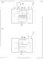
- (A) is a figure which shows the manufacturing process which drops a semiconductor material using an inkjet, in order to form the organic-semiconductor layer in the organic TFT which concerns on Embodiment 1 or 2 of this invention. .
- (B) is a figure which shows the manufacturing process which dripped a semiconductor material using an inkjet in order to form the organic-semiconductor layer in the organic TFT which concerns on Embodiment 3 of this invention. It is sectional drawing of the organic TFT which concerns on Embodiment 4 of this invention.
- a general organic TFT it is a graph which shows the relationship between (i) the water contact angle (horizontal axis) of a gate insulating film, and (ii) the mobility (vertical axis) of the carrier of the organic semiconductor with which an organic TFT is provided. is there.
- FIG. (B) shows the manufacturing process which drippings an insulating material using an inkjet so that the space between the source electrode and drain electrode of the organic TFT which concerns on Embodiment 5 of this invention may not be filled up entirely.
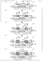
- FIG. (A)-(f) is sectional drawing of the organic TFT which concerns on Embodiment 6 of this invention, and is a figure which shows each process in manufacture of organic TFT.
- (A) is a figure which shows the manufacturing process which forms a 2nd gate insulating layer by dripping an insulating material using the inkjet in the organic TFT which concerns on any one of Embodiment 1 to 5 of this invention. It is.
- a second gate insulating layer is formed in the space between the source electrode first layer and the drain electrode second layer using a spin coater. It is a figure which shows the manufacturing process to do. It is sectional drawing of the organic TFT which concerns on Embodiment 7 of this invention.
- (A) is sectional drawing of the organic TFT which concerns on any one of Embodiment 1 to 6 of this invention, and the gate voltage for controlling the channel of an organic semiconductor is the gate electrode 2nd layer of a gate electrode It is a figure which shows a mode given from.
- FIG. (B) It is sectional drawing of organic TFT which concerns on Embodiment 7 of this invention, and shows a mode that the gate voltage for controlling the channel of an organic semiconductor is given from the gate electrode 2nd layer of the gate electrode
- FIG. (A)-(d) is sectional drawing of the organic TFT which concerns on Embodiment 8 of this invention, and is a figure which shows each process in manufacture of organic TFT.
- (A)-(d) is sectional drawing of the organic TFT which concerns on Embodiment 9 of this invention, and is a figure which shows each process in manufacture of organic TFT.
- FIG. 1 is a cross-sectional view of an organic TFT 1 (semiconductor element) of this embodiment.
- the organic TFT 1 includes a substrate 10, a first gate insulating layer 11, a second gate insulating layer 12, a gate electrode 13, a source electrode 14, a drain electrode 15, and an organic semiconductor layer 16 (semiconductor layer).
- the organic TFT 1 is an organic TFT having a bottom gate structure, and the gate electrode 13 is provided below the source electrode 14 and the drain electrode 15.
- FIG. 1 shows a current path 1 that represents a path of a current that flows from the source electrode 14 side toward the drain electrode 15 side in the organic semiconductor layer 16.
- the substrate 10 is a substrate for disposing various electrodes and insulating layers in the organic TFT 1, and is made of an insulating material such as glass or plastic.
- the substrate 10 may be made of a material such as polyethylene terephthalate or polyimide, for example.
- Gate electrode 13 The gate electrode 13 is provided on the substrate 10.
- the positional relationship in the vertical direction between the members described in detail below is defined with the side of the gate electrode 13 with respect to the substrate 10 as the upper side and the side of the substrate 10 with respect to the gate electrode 13 as the lower side.
- the gate electrode 13 includes a gate electrode first layer 13a as an adhesion layer with the substrate 10, and a gate electrode second layer 13b on the gate electrode first layer 13a.
- the gate electrode first layer 13 a is an adhesion layer that is provided to improve the adhesion between the gate electrode 13 and the substrate 10 and is in contact with the substrate 10.
- the gate electrode first layer 13a is formed of a metal material such as Ti or Cr.
- the gate electrode second layer 13b is an electrode formed of a metal material such as Al (aluminum), and is provided on the gate electrode first layer 13a.
- the gate electrode second layer 13 b functions as a contact layer for electrically connecting the gate electrode 13 to the outside in the organic TFT 1.
- the gate electrode second layer 13b may be formed of a metal material such as Au or Mo (molybdenum) in addition to Al.
- the first gate insulating layer 11 is an insulating layer provided on the upper surfaces of the substrate 10 and the gate electrode 13 so as to cover the surfaces of the substrate 10 and the gate electrode 13.
- the first gate insulating layer 11 may be formed of an organic insulating material such as PVP (polyparavinylphenol), or may be formed of an inorganic insulating material such as SiO 2 (silicon dioxide).
- Source electrode 14 and drain electrode 15 are a source electrode and a drain electrode in the FET, respectively, and are provided on the first gate insulating layer 11 so as to be separated from each other.
- the source electrode 14 includes a source electrode first layer 14a as an adhesion layer with the first gate insulating layer 11, and includes a source electrode second layer 14b on the source electrode first layer 14a. .
- the drain electrode 15 includes a drain electrode first layer 15a as an adhesion layer with the first gate insulating layer 11, and the drain electrode second layer 15b is formed on the drain electrode first layer 15a. I have.
- the source electrode first layer 14a and the drain electrode first layer 15a improve the adhesion between the source electrode 14 and the first gate insulating layer 11 and the adhesion between the drain electrode 15 and the first gate insulating layer 11, respectively. This is an adhesion layer provided to make contact with the first gate insulating layer 11.
- the source electrode first layer 14a and the drain electrode first layer 15a are each formed of a metal material such as Ti or Cr.
- the source electrode second layer 14b is an electrode formed of a metal material such as Au, and is provided on the source electrode first layer 14a.
- the source electrode second layer 14 b functions as a contact layer for electrically connecting the source electrode 14 to the outside and the organic semiconductor layer 16 in the organic TFT 1.
- the drain electrode second layer 15b is an electrode formed of a metal material such as Au, and is provided on the drain electrode first layer 15a.
- the drain electrode second layer 15 b functions as a contact layer for electrically connecting the drain electrode 15 to the outside and the organic semiconductor layer 16 in the organic TFT 1.
- the source electrode 14 and the drain electrode 15 are formed to have the same size.
- d1 (the thickness of the source electrode first layer 14a and the thickness of the drain electrode first layer 15a)
- d2 (the thickness of the source electrode second layer 14b and the thickness of the drain electrode second layer 15b)
- the dimensions d1 and d2 indicating the thickness are respectively determined.
- the source electrode second layer 14b and the drain electrode second layer 15b may be formed of a metal material such as Al or Mo in addition to Au.
- the surfaces facing the drain electrode first layer 15 are the source electrode first layer side surface 14aS and the source electrode second layer side surface 14bS, respectively. It is called.
- the surfaces facing the source electrode first layer 14 are the drain electrode first layer side surface 15aS and the drain electrode second layer side surface 15bS, respectively. It is called.
- the second gate insulating layer 12 is formed on the first gate insulating layer 11 so as to fill a space between the source electrode 14 and the drain electrode 15 that are spaced apart from each other on the first gate insulating layer 11.
- This is an insulating layer provided.
- the term “fill” does not necessarily mean that a member is provided so as to fill the space without a gap, but also means that a member is provided so that there is a gap in a part of the space. ing.
- the material of the second gate insulating layer 12 may be the same insulating material as that of the first gate insulating layer 11, or may be an insulating material different from that of the first gate insulating layer 11.
- a dimension indicating the thickness of the first gate insulating layer 11 is defined as D
- a dimension indicating the thickness of the second gate insulating layer 12 is defined as d.
- the second gate insulating layer 12 covers (i) the entire source electrode first layer side surface 14aS and the entire drain electrode first layer side surface 15aS, and (ii) the source It arrange
- Organic semiconductor layer 16 covers the second gate insulating layer 12 and the source electrode 14 so as to cover the entire surface of the second gate insulating layer 12, a part of the surface of the source electrode 14, and a part of the surface of the drain electrode 15. And on the upper surface of the drain electrode 15.
- the organic semiconductor layer 16 is disposed so as to face the gate electrode 13 with the first gate insulating layer 11 and the second gate insulating layer 12 interposed therebetween.
- the material of the organic semiconductor layer 16 may be a low molecular organic semiconductor material such as tetracene, or may be a high molecular organic semiconductor material such as PPV (polyparaphenylene vinylene).
- a P-type organic semiconductor is generally used as the organic semiconductor layer 16 in the organic TFT 1, and the organic semiconductor layer 16 in the present embodiment is also formed as a P-type organic semiconductor layer.
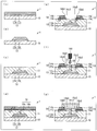
- FIGS. 2A to 2G are cross-sectional views of the organic TFT 1, respectively, illustrating each step in the manufacture of the organic TFT 1.
- FIG. 2A shows a gate electrode first layer base material as a step before forming the gate electrode first layer 13a and the gate electrode second layer 13b, which are two layers included in the gate electrode 13 in the organic TFT 1.
- 7 is a diagram showing a step (first step, step (a1)) of forming a gate electrode layer base material 17 composed of 17a and a gate electrode second layer base material 17b on the entire upper surface of the substrate 10.
- a layer of a material functioning as an adhesion layer is formed on the entire upper surface of the substrate 10 by a known method such as a CVD (Chemical Vapor Deposition) method or a PVD (Physical Vapor Deposition) method.
- a CVD Chemical Vapor Deposition
- PVD Physical Vapor Deposition
- a gate electrode first layer base material 17a Ti is selected as the material of the gate electrode first layer base material 17a, and the gate electrode first layer base material 17a is formed with a thickness of 10 nm.
- a layer of a material functioning as a contact layer of the organic TFT 1 is formed on the entire upper surface of the gate electrode first layer base material 17a by a known method in the same manner as the gate electrode first layer base material 17a.
- a gate electrode second layer base material 17b is formed on the entire upper surface of the gate electrode first layer base material 17a by a known method in the same manner as the gate electrode first layer base material 17a.
- Al is selected as the material of the gate electrode second layer base material 17b, and the gate electrode second layer base material 17b is formed with a thickness of 300 nm.
- FIG. 2B includes a gate electrode first layer 13a and a gate electrode second layer 13b from a gate electrode layer base material 17 composed of a gate electrode first layer base material 17a and a gate electrode second layer base material 17b. It is a figure which shows the process (2nd process, process (b1)) which forms the gate electrode.
- the gate electrode 13 is formed on the gate electrode layer base material 17 covering the entire top surface of the substrate 10 by photolithography using a known photolithography technique.
- gate electrode 13 patterning for forming the gate electrode 13 is performed by photolithography, and unnecessary gate electrode layer base material 17 (that is, unnecessary gate electrode first layer base material 17a and gate electrode second layer base material 17b) is formed. By removing, the gate electrode 13 is formed.
- FIG. 2B the gate electrode layer base material 17 located near both ends of the substrate 10 is removed, and the gate electrode layer base material 17 located near the center of the substrate 10 is left. The case where the electrode 13 is formed is illustrated.
- the gate electrode first layer 13a and the gate electrode second layer 13b of the gate electrode 13 correspond to the gate electrode first layer base material 17a and the gate electrode second layer base material 17b of the gate electrode layer base material 17, respectively. It is a member.
- a photoresist mask (not shown) patterned by a known photolithography technique is provided on a gate electrode layer base material 17 present at a position corresponding to the gate electrode 13.
- the photoresist mask is removed by ashing or the like after the gate electrode 13 is formed.
- FIG. 2C is a diagram showing a step of forming the first gate insulating layer 11 on the entire upper surface of the substrate 10 and the gate electrode 13 (third step, step (c1)).
- the first gate insulating layer 11 is formed on the entire upper surface of the substrate 10 and the gate electrode 13 by, for example, forming a layer of an insulating material with a predetermined thickness using a spin coater.
- PVP is selected as the material of the first gate insulating layer 11, and the first gate insulating layer 11 is formed with a thickness of 500 nm.
- the apparatus which forms the 1st gate insulating layer 11 in a 3rd process is not limited to a spin coater, You may use the other apparatus for forming arbitrary well-known thin films.
- FIG. 2D shows (i) two layers included in the source electrode 14, that is, a source electrode first layer 14 a and a source electrode second layer 14 b, and (ii) two layers included in the drain electrode 15.
- a source / drain electrode layer base material comprising a source / drain electrode first layer base material 18a and a source / drain electrode second layer base material 18b as a step before forming a certain drain electrode first layer 15a and drain electrode second layer 15b.
- 18 is a diagram illustrating a step of forming a film 18 on the entire upper surface of the first gate insulating layer 11 (fourth step, step (d1)).
- a layer of a material functioning as an adhesion layer is formed on the entire upper surface of the first gate insulating layer 11 in a predetermined thickness by a known method, similarly to the gate electrode first layer base material 17a.
- a source / drain electrode first layer base material 18a is formed by film formation.
- Ti is selected as the material of the source / drain electrode first layer base material 18a, and the source / drain electrode first layer base material 18a is formed to have a thickness of 10 nm.
- a layer of a material functioning as a contact layer of the organic TFT 1 is formed on the entire upper surface of the source / drain electrode first layer base material 18a by a known method in the same manner as the source / drain electrode first layer base material 18a.
- the source / drain electrode second layer base material 18b is formed by forming a film with a thickness.
- Au is selected as the material of the source / drain electrode second layer base material 18b, and the source / drain electrode second layer base material 18b is formed to have a thickness of 100 nm.
- the thickness of the source / drain electrode first layer base material 18a formed in the fourth step is the thickness of the source electrode first layer 14a of the organic TFT 1 and the thickness of the drain electrode first layer 15a (ie, d1). be equivalent to.
- the thickness of the source / drain electrode second layer base material 18b is equal to the thickness of the source electrode second layer 14b of the organic TFT 1 and the thickness of the drain electrode second layer 15b (that is, d2).
- FIG. 2E shows a source / drain electrode layer base material 18 composed of a source / drain electrode first layer base material 18a and a source / drain electrode second layer base material 18b, and (i) a source electrode first layer 14a and a source electrode.
- the source / drain electrode layer base material 18 covering the entire upper surface of the first gate insulating layer 11 is subjected to photolithography by a known photolithography technique to form the source electrode 14 and the drain electrode 15.
- the unnecessary source / drain electrode layer base material 18 that is, the unnecessary source / drain electrode first layer base material 18a and the source / drain electrode first layer are formed.
- the source electrode 14 and the drain electrode 15 which are separated from each other are formed on the first gate insulating layer 11.
- the source electrode 14 is disposed on the side facing one of the two side surfaces of the gate electrode 13 (that is, the left side) in the horizontal direction, and the drain electrode 15 is A case is illustrated in which the gate electrode 13 is disposed on the side (that is, the right side) opposite to the other of the two side surfaces.
- a photoresist mask (not shown) patterned by a well-known photolithography technique is provided on a source / drain electrode layer base material 18 present at a position corresponding to each of the source electrode 14 and the drain electrode 15. Yes.
- the photoresist mask is removed by ashing or the like after the source electrode 14 and the drain electrode 15 are formed. Moreover, you may add the process of removing the residue adhering to circumference
- FIG. 2F shows the first gate insulating layer 11 on the first gate insulating layer 11 so as to fill a space between the source electrode 14 and the drain electrode 15 that are spaced apart from each other on the first gate insulating layer 11. It is a figure which shows the process (6th process, process (f1)) which forms the 2nd gate insulating layer 12.
- FIG. 6th process, process (f1) shows the process (6th process, process (f1) which forms the 2nd gate insulating layer 12.
- the insulating material 56 is dropped over the entire upper surface of the first gate insulating layer 11 using the ink jet 190 so as to fill the space between the source electrode 14 and the drain electrode 15.
- the second gate insulating layer 12 is formed by depositing these layers at a predetermined thickness.
- the second gate insulating layer 12 covers (i) the entire source electrode first layer side surface 14aS and the entire drain electrode first layer side surface 15aS, and (ii) the source electrode second layer side surface 14bS.
- the drain electrode second layer side surface 15bS is disposed between the source electrode 14 and the drain electrode 15 so as to cover a part thereof.
- the surface energy of the first gate insulating layer 11 is added to the first gate insulating layer 11 obtained in the first gate insulating layer forming step between the first gate insulating layer forming step and the second gate insulating layer forming step. May further include a surface treatment step of performing a surface treatment for making the value larger than the value of the surface energy of the second gate insulating layer 12. The effect obtained by the difference between the surface energy of the first gate 11 and the surface energy of the second gate insulating layer 12 will be described in detail in Embodiments 3 and 4 described later.
- FIG. 2G shows the second gate insulating layer 12 and the source so as to cover the entire surface of the second gate insulating layer 12, a part of the surface of the source electrode 14, and a part of the surface of the drain electrode 15. It is a figure which shows the process (7th process, process (g1)) which forms the organic-semiconductor layer 16 on the upper surface of the electrode 14 and the drain electrode 15.
- FIG. 7th process, process (g1) which forms the organic-semiconductor layer 16 on the upper surface of the electrode 14 and the drain electrode 15.
- the organic semiconductor material layer is formed on the entire surface of the second gate insulating layer 12 and the surface of the source electrode 14 using a known method such as vacuum deposition (for example, an ink jet method or a spin coating method). A part of the surface of the drain electrode 15 is partially covered with the second gate insulating layer 12, the source electrode 14, and the drain electrode 15, and the organic semiconductor layer 16 is formed.
- the organic semiconductor layer 16 is formed to face the gate electrode 13 with the first gate insulating layer 11 and the second gate insulating layer 12 interposed therebetween.
- PPV is selected as the material of the organic semiconductor layer 16, and the thickness of the organic semiconductor layer is set to 200 nm.
- the organic TFT 1 of this embodiment is formed by the manufacturing processes from the first process to the seventh process described above in FIGS. 2 (a) to 2 (g).
- the surface energy of the second gate insulating layer 12 is transferred to the second gate insulating layer 12 obtained in the second gate insulating layer forming step. It may further include a surface treatment step of performing a surface treatment for making the value larger than the value of the surface energy.
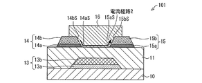
- FIG. 3 is a cross-sectional view of an organic TFT 101 as a comparative example. A configuration similar to that of the organic TFT 101 of FIG. 3 is disclosed in Non-Patent Document 2 described above.
- Each member included in the organic TFT 101 as a comparative example includes a substrate 10, a first gate insulating layer 11, a gate electrode 13, a source electrode 14, a drain electrode 15, and an organic semiconductor layer 16.
- each member with which organic TFT101 as a comparative example is provided is the same as each member with which organic TFT1 of this embodiment is provided, it shows using the same member number.
- the organic TFT 101 as a comparative example has a configuration in which the second gate insulating layer 12 is excluded from the organic TFT 1 of the present embodiment, and the space where the second gate insulating layer 12 in the organic TFT 1 of the present embodiment exists is It has a structure obtained by filling with the organic semiconductor layer 16.
- FIG. 3 shows a current path 2 representing a path of a current flowing from the source electrode 14 side toward the drain electrode 15 side in the organic semiconductor layer 16 included in the organic TFT 101 as a comparative example.
- the organic semiconductor layer 16 is electrically connected to (i) the source electrode first layer 14 a of the source electrode 14 and (ii) the drain electrode first layer 15 a of the drain electrode 15.
- the organic semiconductor layer 16 is electrically connected to (i) the source electrode second layer 14 b of the source electrode 14 and (ii) the drain electrode second layer 15 b of the drain electrode 15.
- the organic semiconductor layer 16 in the organic TFT 101 is a P-type organic semiconductor and has a work function of about 5.0 eV.
- the source electrode second layer 14b and the drain electrode second layer 15b which function as the electrodes of the source electrode 14 and the drain electrode 11, respectively, are formed of a material such as Au.
- the source electrode second layer 14b and the drain electrode second layer 15b are made of Au, they have a work function of about 4.8 eV.
- the source electrode second layer 14b and the drain electrode second layer 15b are not limited to Au, and may be formed of a material such as Cu (copper) or Ni (nickel).
- the source electrode second layer 14b and the drain electrode second layer 15b are made of Cu, they have a work function of about 4.7 eV.
- the source electrode second layer 14b and the drain electrode second layer 15b have a work function of about 5.2 eV when formed of Ni.
- the organic semiconductor layer 16 and the source electrode second layer 14b, and (ii) the organic semiconductor layer 16 and the drain electrode second layer 15b each have a work function of approximately the same size. Therefore, good contact can be made with each other. For this reason, the value of the contact resistance between (i) the organic semiconductor layer 16 and the source electrode second layer 14b and (ii) between the organic semiconductor layer 16 and the drain electrode second layer 15b is low. An amount of current can flow.
- the source electrode first layer 14a and the drain electrode first layer 15a are formed of a material such as Ti.
- the source electrode first layer 14a and the drain electrode first layer 15a have a work function having a magnitude of about 4.0 eV.
- the organic semiconductor layer 16 and the source electrode first layer 14a, and (ii) the organic semiconductor layer 16 and the drain electrode second layer 15a have different work functions, respectively. They cannot make good contact with each other. For this reason, the value of contact resistance between (i) the organic semiconductor layer 16 and the source electrode first layer 14a and (ii) between the organic semiconductor layer 16 and the drain electrode first layer 15a is high. An amount of current cannot flow.
- the contact resistance value between the source electrode second layer 14 b and the organic semiconductor layer 16 is smaller than the contact resistance value between the source electrode first layer 14 a and the organic semiconductor layer 16.
- the contact resistance value between the drain electrode second layer 15 b and the organic semiconductor layer 16 is smaller than the contact resistance value between the drain electrode first layer 15 a and the organic semiconductor layer 16.
- a channel is formed near the interface of the first gate insulating layer 11 between the source electrode 14 and the drain electrode 15, and a current flows inside the channel. Therefore, the current flowing from the source electrode 14 to the drain electrode 15 starts from the source electrode second layer 14b of the source electrode 14, and then reaches the drain electrode second layer 15b of the drain electrode 15. (Current path 2) passing through the vicinity of the interface of the first gate insulating layer 11 between the source electrode 14 and the drain electrode 11, It flows through the organic semiconductor layer 16 through the above (current path 2).
- the organic TFT 1 of this embodiment includes a second gate insulating layer 12 between the source electrode 14 and the drain electrode 15.
- the organic TFT 1 of this embodiment is different from the organic TFT 101 as a comparative example in this point.
- the contact resistance value between the source electrode second layer 14 b and the organic semiconductor layer 16 is the contact between the source electrode first layer 14 a and the organic semiconductor layer 16. Less than the resistance value.
- the contact resistance value between the drain electrode second layer 15 b and the organic semiconductor layer 16 is smaller than the contact resistance value between the drain electrode first layer 15 a and the organic semiconductor layer 16.
- a channel is formed near the interface of the second gate insulating layer 12 between the source electrode 14 and the drain electrode 15, and current flows inside the channel. Therefore, the current flowing from the source electrode 14 to the drain electrode 15 starts from the source electrode second layer 14b of the source electrode 14, and then reaches the drain electrode second layer 15b of the drain electrode 15. (Current path 1) It passes through the vicinity of the interface of the second gate insulating layer 12 between the source electrode 4 and the drain electrode 15. It flows through the organic semiconductor layer 16 through the above (current path 1).
- (current path 1) is a path located on the upper surface of the second gate insulating layer 12 that covers the entire source electrode first layer side surface 14aS and the entire drain electrode first layer side surface 15aS. . Therefore, in (current path 1), (i) contact between the organic semiconductor layer 16 and the source electrode first layer 14a, and (ii) contact between the organic semiconductor layer 16 and the drain electrode first layer 15a. The effect of resistance is eliminated.
- the organic TFT 1 of the present embodiment can suppress the deterioration of the characteristics of the organic TFT 1 by further providing the second gate insulating layer 12.
- a semiconductor element having a structure similar to that of the organic TFT 1 of the present embodiment for example, an inorganic semiconductor layer having the same physical characteristics as the organic semiconductor layer 16 of the present embodiment (for example, a work function value)) (for example, The above-described effects can also be achieved by manufacturing an inorganic TFT).
- Organic TFT 101a and 101b As another comparative example of the organic TFT 1 of this embodiment, an organic TFT 101a shown in FIG. 4A and an organic TFT 101b shown in FIG. 4B will be described.
- FIG. 4A is a cross-sectional view of an organic TFT 101a as another comparative example of the organic TFT 1 of the present embodiment.
- the organic TFT 101a includes a substrate 10, a first gate insulating layer 11a, a second gate insulating layer 12a, a gate electrode 13, a source electrode 14, a drain electrode 15, and an organic semiconductor layer 16.
- each member included in the organic TFT 101a as the comparative example is the same as each member included in the organic TFT 1 of the present embodiment except for the first gate insulating layer 11a and the second gate insulating layer 12a. , Using the same member numbers.
- the second gate insulating layer 12a in the organic TFT 101a has a structure equivalent to the planarization layer provided between the source electrode 14 and the drain electrode 15 in Patent Document 1.
- the first gate insulating layer 11a when the dimension indicating the thickness from the upper surface of the gate electrode second layer 13b to the upper surface of the first gate insulating layer 11a is Da, the dimension da is between the dimension Da and the dimension Da. , da ⁇ Da The relationship is established. That is, the first gate insulating layer 11a in the organic TFT 101a is a thick insulating film having the same thickness as the second gate insulating layer 12a.
- the organic TFT 101a since the first gate insulating layer 11a and the second gate insulating layer 12a have both thick dimensions, the amount of current flowing inside the organic semiconductor layer 16 is reduced, and the organic TFT 101a Degradation of characteristics occurs.
- FIG. 4B is a cross-sectional view of an organic TFT 101b as another comparative example of the organic TFT 1 of the present embodiment.
- the organic TFT 101b includes a substrate 10, a first gate insulating layer 11b, a second gate insulating layer 12b, a gate electrode 13, a source electrode 14, a drain electrode 15, and an organic semiconductor layer 16.
- each member included in the organic TFT 101b as the comparative example is the same as each member included in the organic TFT 1 of the present embodiment except for the first gate insulating layer 11b and the second gate insulating layer 12b. , Using the same member numbers.
- the second gate insulating layer 12b in the organic TFT 101b has a structure equivalent to a planarization layer provided between the source electrode 14 and the drain electrode 15 in Patent Document 1.
- the second gate insulating layer 12b in the organic TFT 101b is a thin insulating film having a sufficiently smaller thickness than the first gate insulating layer 11b.
- the second gate insulating layer 12b in the organic TFT 101b has a thinner dimension than the second gate insulating layer 12a in the organic TFT 101a. For this reason, the organic TFT 101b can flow a larger current than the organic TFT 101a, and can realize higher characteristics than the organic TFT 101a.
- the organic TFT 101b since the second gate insulating layer 12b is thin, (i) the dielectric strength between the gate electrode 13 and the source electrode 14, and (ii) between the gate electrode 13 and the drain electrode 15, The dielectric strength is lower than that of the organic TFT 101a. For this reason, the organic TFT 101b is less resistant to a high voltage than the organic TFT 101a, and is inferior in device reliability.
- the organic TFT 1 of the present embodiment can achieve both device characteristics and reliability by providing the second gate insulating layer 12 that satisfies the above-described formula (1). Therefore, it is realized as an excellent device as compared with the organic TFT 101a and the organic TFT 101b as comparative examples.
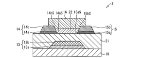
- FIG. 5 is a cross-sectional view of the organic TFT 2 (semiconductor element) of this embodiment.
- the organic TFT 2 includes a substrate 10, a first gate insulating layer 21, a second gate insulating layer 22, a gate electrode 13, a source electrode 14, a drain electrode 15, and an organic semiconductor layer 16.
- each member included in the organic TFT 2 of Embodiment 2 is the same as each member included in the organic TFT 1 of Embodiment 1 except for the first gate insulating layer 21 and the second gate insulating layer 22.
- the same member numbers are used.
- the first gate insulating layer 21 is an insulating layer provided on the upper surfaces of the substrate 10 and the gate electrode 13 so as to cover the surfaces of the substrate 10 and the gate electrode 13.
- the first gate insulating layer 21 in the organic TFT 2 is formed of a material having a dielectric constant higher than that of the second gate insulating layer 22.
- the dielectric constant ⁇ 1 of the first gate insulating layer 21 is obtained by using the vacuum dielectric constant ⁇ 0 .
- the material of the first gate insulating layer 21 is not limited to PVP, and any material having a higher dielectric constant than that of the second gate insulating layer 22 may be used. Other suitable high dielectric constants that can ensure insulation performance. (High-k material) may be used.
- the second gate insulating layer 22 is formed on the first gate insulating layer 21 so as to fill a space between the source electrode 14 and the drain electrode 15 that are spaced apart from each other on the first gate insulating layer 21.
- An insulating layer provided.
- the material of the second gate insulating layer 22 is formed of a material having a lower dielectric constant than that of the first gate insulating layer 21.
- CYTOP registered trademark
- amorphous fluororesin manufactured by Asahi Glass Co., Ltd.
- ⁇ r2 2.0
- the material of the second gate insulating layer 22 is not limited to CYTOP, and any material having a lower dielectric constant than that of the first gate insulating layer 21 may be used. Other suitable low dielectric constants that can ensure the insulating performance. (Low-k material) may be used.
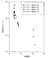
- FIG. 6 shows the relationship between (i) the relative dielectric constant of the gate insulating film (horizontal axis) and (ii) the mobility of carriers of the organic semiconductor included in the organic TFT (vertical axis) in a general organic TFT. It is a graph which shows.
- FIG. 6 is a graph disclosed in Non-Patent Document 3 described above, and shows data on an organic TFT having a top gate structure and a bottom gate structure.
- the organic TFT having a top gate structure refers to an organic TFT having a structure in which a gate electrode is provided above the source electrode and the drain electrode.
- the organic TFT having the bottom gate structure refers to an organic TFT having a structure in which the gate electrode is provided below the source electrode and the drain electrode, and has the same structure as the organic TFT 2 of the present embodiment.
- the organic TFT in FIG. 6 is formed of PTTA (polytriallylamine), and data is shown for PTTA1 and PTTA2, which are different PTTAs.
- PTTA polytriallylamine
- FIG. 6 shows that the mobility of the carrier of the organic semiconductor increases as the relative dielectric constant of the gate insulating film in the organic TFT decreases regardless of the semiconductor material. Therefore, the carrier mobility of the organic semiconductor can be increased by lowering the value of the dielectric constant of the gate insulating film in contact with the organic semiconductor.
- the mobility of carriers in the organic semiconductor layer 16 can be increased by forming the second gate insulating layer 22 in contact with the organic semiconductor layer 16 with a material having a low dielectric constant. . Therefore, the characteristics of the organic TFT 2 can be improved.
- a material having a high dielectric constant that is, a high relative dielectric constant
- Si silicon
- a material having a high dielectric constant that is, a high relative dielectric constant
- the amount of current flowing from the source to the drain of the field effect transistor is defined by the capacitance value of the gate insulating layer, and as the capacitance value of the gate insulating layer increases, the amount of current flowing from the source to the drain is increased. This is because a larger amount of current can flow.
- the capacitance C of the gate insulating layer is expressed by the following equation (2) using the thickness d of the gate insulating layer, the surface area S of the gate insulating layer, and the dielectric constant ⁇ of the gate insulating layer. .
- the thickness d of the gate insulating layer can be increased by using an insulating material having a large dielectric constant ⁇ as the material of the gate insulating layer, In order to prevent leakage current and dielectric breakdown, it is possible to design to ensure the insulation performance of the field effect transistor.
- a material having a high dielectric constant ⁇ is used as the material of the first gate insulating layer 21 that is not in contact with the organic semiconductor layer 16. Therefore, also in the organic TFT 2, it is possible to ensure both the current characteristics and the insulation performance of the organic TFT 2 as in the case of the conventional field effect transistor using the inorganic semiconductor layer.
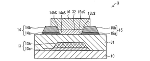
- FIG. 7 is a cross-sectional view of the organic TFT 3 (semiconductor element) of this embodiment.
- the organic TFT 3 includes a substrate 10, a first gate insulating layer 31, a second gate insulating layer 32, a gate electrode 13, a source electrode 14, a drain electrode 15, and an organic semiconductor layer 16.
- each member included in the organic TFT 3 of Embodiment 3 is the same as each member included in the organic TFT 1 of Embodiment 1 except for the first gate insulating layer 31 and the second gate insulating layer 32.
- the same member numbers are used.
- the first gate insulating layer 31 is an insulating layer provided on the upper surfaces of the substrate 10 and the gate electrode 13 so as to cover the surfaces of the substrate 10 and the gate electrode 13.
- the first gate insulating layer 31 in the organic TFT 3 is formed to have a surface energy smaller than that of the second gate insulating layer 32. That is, as the material of the first gate insulating layer 31, a material having a surface energy smaller than that of the second gate insulating layer 32 is selected.
- the first gate insulating layer 31 in the organic TFT 3 can be formed of the same material as the second gate insulating layer 32.
- the surface of the second gate insulating layer 32 is irradiated with UV (Ultra-Violet) light and subjected to surface modification, whereby the second gate insulating layer 32 having a surface energy larger than that of the first gate insulating layer 31 is obtained.
- the second gate insulating layer 32 having a surface energy larger than that of the first gate insulating layer 31 may be formed by applying a monomolecular film such as a silane coupling agent on the surface of the second gate insulating layer 32. Good.
- the second gate insulating layer 32 is formed on the first gate insulating layer 31 so as to fill a space between the source electrode 14 and the drain electrode 15 that are spaced apart from each other on the first gate insulating layer 31. This is an insulating layer provided.
- the second gate insulating layer 32 in the organic TFT 3 is formed to have a larger surface energy than the first gate insulating layer 31. That is, as the material of the second gate insulating layer 32, a material having a larger surface energy than the material of the first gate insulating layer 31 is selected.
- the second gate insulating layer 32 can be formed of the same material as the first gate insulating layer 31.
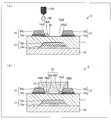
- FIG. 8B shows the second gate insulating layer so as to cover the entire surface of the second gate insulating layer 32 of the organic TFT 3, a part of the surface of the source electrode 14, and a part of the surface of the drain electrode 15.
- a manufacturing step in order to form the organic semiconductor layer 16 on the upper surfaces of the source electrode 14 and the drain electrode 15, a manufacturing step (in the seventh step (step (g1) in the first embodiment) in which the semiconductor material 36 is dropped using the inkjet 190.
- the organic TFT 3a is equivalent to the organic TFT according to any of the first or second embodiment described above.
- the organic TFT 3a is equivalent to the organic TFT 1 according to the first embodiment.
- each member included in the organic TFT 3a as the comparative example is the same as each member included in the organic TFT 3 of Embodiment 3 except for the first gate insulating layer 31a and the second gate insulating layer 32a. , Using the same member numbers.
- the surface energy ES2 of the second gate insulating layer 32 is larger than the surface energy ES1 of the first gate insulating layer 31 in the organic TFT 3 of the present embodiment (that is, ES1 ⁇ ES2) is different.
- FIG. 8A shows the second gate insulating layer so as to cover the entire surface of the second gate insulating layer 32a of the organic TFT 3a, a part of the surface of the source electrode 14, and a part of the surface of the drain electrode 15.
- 32a manufacturing process in which the semiconductor material 36 is dropped using the ink jet 190 to form the organic semiconductor layer 16 on the upper surfaces of the source electrode 14 and the drain electrode 15 (seventh process in the first embodiment (process (g1))
- the semiconductor material 36 is dropped when the semiconductor material 36 is dropped onto the upper surface of the second gate insulating layer 32a using the inkjet 190. 36 is not necessarily dropped into a region corresponding to the upper surface of the second gate insulating layer 32a.
- the magnitude of the surface energy ES2a of the second gate insulating layer 32a and the magnitude of the surface energy ES1a of the first gate insulating layer 31a are both equal.
- the second gate insulating layer 32 a and the first gate insulating layer 31 a both form an equal contact angle with respect to the droplet of the semiconductor material 36. That is, the second gate insulating layer 32 a and the first gate insulating layer 31 a have the same wettability with respect to the droplets of the semiconductor material 36.
- the organic semiconductor layer 16 in the organic TFT 3a may not be uniformly formed in a region corresponding to the upper surface of the second gate insulating layer 32a.
- FIG. 8B a part of the semiconductor material 36 dropped by using the ink jet 190 is displaced from the region corresponding to the upper surface of the second gate insulating layer 32, and the first gate. A case is assumed that is located above the insulating layer 31.
- the surface energy ES2 of the second gate insulating layer 32 is larger than the surface energy ES1 of the first gate insulating layer 31.
- the second gate insulating layer 32 forms a smaller contact angle with respect to the droplet of the semiconductor material 36 than the first gate insulating layer 31. That is, the second gate insulating layer 32 has higher wettability with respect to the droplets of the semiconductor material 36 than the first gate insulating layer 31.
- a part of the semiconductor material 36 dropped on the first gate insulating layer 31 is repelled from the surface of the first gate insulating layer 31 and wets and spreads toward the second gate insulating layer 32 side.
- a part of the semiconductor material 36 dropped onto the upper portion of the first gate insulating layer 31 moves to the second gate insulating layer 32 side, and is crystallized after drying over time.
- the organic semiconductor layer 16 in the organic TFT 3 is uniformly formed in a region corresponding to the upper surface of the second gate insulating layer 32. Thereby, the characteristics of the organic TFT 3 can be further improved.
- FIG. 9 is a cross-sectional view of the organic TFT 4 (semiconductor element) of this embodiment.
- the organic TFT 4 includes a substrate 10, a first gate insulating layer 41, a second gate insulating layer 42, a gate electrode 13, a source electrode 14, a drain electrode 15, and an organic semiconductor layer 16.
- each member included in the organic TFT 4 of Embodiment 4 is the same as each member included in the organic TFT 1 of Embodiment 1 except for the first gate insulating layer 41 and the second gate insulating layer 42.
- the same member numbers are used.
- the first gate insulating layer 41 is an insulating layer provided on the upper surfaces of the substrate 10 and the gate electrode 13 so as to cover the surfaces of the substrate 10 and the gate electrode 13.
- the first gate insulating layer 41 in the organic TFT 4 is formed to have a larger surface energy than the second gate insulating layer 42.
- the first gate insulating layer 41 in the organic TFT 4 is different from the point that the first gate insulating layer 31 in the organic TFT 3 is formed to have a surface energy smaller than that of the second gate insulating layer 32. .
- the material of the first gate insulating layer 41 a material having a larger surface energy than that of the second gate insulating layer 42 may be used.
- the first gate insulating layer 41 can be formed of the same material as the second gate insulating layer 42 as in the third embodiment. That is, the first gate having a surface energy larger than that of the second gate insulating layer 42 by irradiating the surface of the first gate insulating layer 41 with UV light or applying a monomolecular film such as a silane coupling agent.
- the insulating layer 41 may be formed.
- the surface treatment for increasing the surface energy is performed on the surface of the first gate insulating layer 41 (for example, the step of irradiating the surface of the first gate insulating layer 41 with UV light, or the silane coupling agent And the like) may be performed prior to the step of forming the source electrode 14 and the drain electrode 15 or after the step of forming the source electrode 14 and the drain electrode 15. Good.
- the second gate insulating layer 42 is formed on the first gate insulating layer 41 so as to fill a space between the source electrode 14 and the drain electrode 15 that are spaced apart from each other on the first gate insulating layer 41. This is an insulating layer provided.
- the second gate insulating layer 42 in the organic TFT 4 is formed to have a surface energy smaller than that of the first gate insulating layer 41. That is, if the surface energy value of the first gate insulating layer 41 is ES1 and the surface energy value of the second gate insulating layer 42 is ES2, the relationship ES1> ES2 is established.
- the second gate insulating layer 42 in the organic TFT 4 is formed such that the second gate insulating layer 32 in the organic TFT 3 has a surface energy larger than that of the first gate insulating layer 31 (that is, ES1 ⁇ ES2). It is different from that.
- the material of the second gate insulating layer 42 may be a material having a surface energy smaller than that of the first gate insulating layer 41.
- the same material as that of the first gate insulating layer 41 may be used.
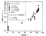
- FIG. 10 shows the relationship between (i) the water contact angle (horizontal axis) of the gate insulating film and (ii) the mobility (vertical axis) of the carrier of the organic semiconductor provided in the organic TFT in a general organic TFT. It is a graph which shows.
- FIG. 10 is a graph disclosed in Non-Patent Document 4 described above, and shows data on each material of the gate insulating film for the bottom contact type organic TFT having the bottom gate structure. Note that the gate insulating film in FIG. 10 is formed of SAM (Self-Assembled Monolayer).
- FIG. 10 shows a tendency that the mobility of the organic semiconductor carrier increases as the value of the water contact angle of the gate insulating film in the organic TFT increases. Therefore, it can be argued that the carrier mobility of the organic semiconductor increases as the surface energy value of the gate insulating film in the organic TFT decreases.
- the mobility of the organic semiconductor carrier can be increased.
- the mobility of carriers in the organic semiconductor layer 16 can be increased by forming the second gate insulating layer 42 in contact with the organic semiconductor layer 16 with a material having a small surface energy. . Therefore, the characteristics of the organic TFT 4 can be improved.
- the organic semiconductor layer 16 is formed using an apparatus that is different from the inkjet 190 in the third embodiment and does not require highly precise position controllability (for example, using the spin coat apparatus, the second gate insulating layer 42).
- the organic TFT 4 of Embodiment 4 can be easily configured. Therefore, a device having excellent characteristics can be realized.
- FIG. 11B is a cross-sectional view of the organic TFT 5.
- the organic TFT 5 includes a substrate 10, a first gate insulating layer 11, a second gate insulating layer 52, a gate electrode 13, a source electrode 14, a drain electrode 15, and an organic semiconductor layer 16.
- each member with which the organic TFT 5 of Embodiment 5 is provided is the same as each member with which the organic TFT 1 of Embodiment 1 is provided except for the second gate insulating layer 52, the same member number is used. Show.
- the second gate insulating layer 52 includes a source-side second gate insulating layer 52a and a drain-side second gate insulating layer 52b.
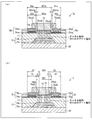
- FIG. 11A shows a manufacturing process (implementation) in which an insulating material 56 is dropped into a space between the source electrode 14 and the drain electrode 15 using the inkjet 190 in order to form the second gate insulating layer 52. It is a figure which shows the 6th process (equivalent to a process (f1)) in the form 1.
- the insulating material 56 dropped in FIG. 11A is used to form the source-side second gate insulating layer 52a.
- the second gate insulating layer 52 is an insulating layer provided on the first gate insulating layer 11, and is disposed between the source electrode 14 and the drain electrode 15 that are spaced apart from each other on the first gate insulating layer 11. It is provided in the space.
- the second gate insulating layer 52 includes a source-side second gate insulating layer 52a and a drain-side second gate insulating layer 52b.
- the source-side second gate insulating layer 52a is in contact with the source electrode 14, and is provided so as to cover the entire source electrode first layer side surface 14aS and a portion of the source electrode second layer side surface 14bS. It has been.
- the drain-side second gate insulating layer 52b is in contact with the drain electrode 15, and is provided so as to cover the entire drain electrode first layer side surface 15aS and to cover a part of the drain electrode second layer side surface 15bS. It has been.
- the source-side second gate insulating layer 52a and the drain-side second gate insulating layer 52b are provided to be separated from each other. That is, the source-side second gate insulating layer 52a and the drain-side second gate insulating layer 52b are not in contact with each other.
- the second gate insulating layer 52 in the organic TFT 5 is formed so as not to entirely fill the space between the source electrode 14 and the drain electrode 15.
- the second gate insulating layer 52 of the present embodiment is different from the first gate insulating layers 12, 22, 32, and 42 in the first to fourth embodiments between the source electrode 14 and the drain electrode 15. It differs from the point which is formed so that the space of this may be filled up entirely.
- the organic semiconductor layer 16 is formed so as to fill a space between the source-side second gate insulating layer 52a and the drain-side second gate insulating layer 52b.
- FIG. 12B shows a manufacturing process in which the insulating material 56 is dropped using the inkjet 190 so as not to fill the entire space between the source electrode 14 and the drain electrode 15 of the organic TFT 5a (Embodiment 1). It is a figure which shows the 6th process in FIG.
- the organic TFT 5a is equivalent to the organic TFT according to any one of the first to fourth embodiments described above, and is equivalent to, for example, the organic TFT 1 of the first embodiment. Since each member with which organic TFT5a is provided is the same as that with which organic TFT1 of Embodiment 1 is provided, it shows using the same member number.
- FIG. 12A shows a manufacturing process in which the insulating material 56 is dropped using the inkjet 190 so as to fill the entire space between the source electrode 14 and the drain electrode 15 of the organic TFT 5a (Embodiment 1). It is a figure which shows the 6th process (equivalent to process (f1)) in FIG.
- the insulating material 56 is dropped from the inkjet 190 onto the upper surface of the first gate insulating layer 11 so as to fill the entire space between the source electrode 14 and the drain electrode 15.
- the second gate insulating layer 12 included in the organic TFT 5a is formed from the insulating material 56 so as to fill the space between the source electrode 14 and the drain electrode 15 as a whole.
- the insulating material 56 is disposed so as to entirely fill the space between the source electrode 14 and the drain electrode 15 by dropping the insulating material 56 from the inkjet 190 a plurality of times. Yes.
- the insulating material 56 is removed from the inkjet 190 so as to contact (i) the source electrode 14 and (ii) contact the drain electrode. , Dropped on the upper surface of the first gate insulating layer 11.
- the insulating material 56 located on the upper surface of the one gate insulating layer 11 is provided so as not to contact each other.
- the source-side second gate insulating layer 52a that is in contact with the source electrode 14 is formed from the insulating material 56 that is dropped so as to be in contact with the source electrode 14 and is located on the upper surface of the first gate insulating layer 11.
- the drain-side second gate insulating layer 52 b in contact with the drain electrode 15 is formed from the insulating material 56 that is dropped so as to be in contact with the drain electrode 15 and located on the upper surface of the first gate insulating layer 11. .
- the source-side second gate insulating layer 52a and the drain-side second gate insulating layer 52b are not in contact with each other.
- the second gate insulating layer 52 of the organic TFT 5 is formed by partially dropping an insulating material 56 so as to be in contact with the source electrode 14 and the drain electrode 15. Therefore, the second gate insulating layer 52 of the organic TFT 5 is formed with a smaller number of drops of the insulating material 56 than the second gate insulating layer 12 of the organic TFT 5a.
- the only insulating layer covering the region near the center of the channel of the organic semiconductor layer 16 is the first gate insulating layer 11 having a uniform film thickness.
- the second gate insulating layer 52 does not cover a region near the center of the channel of the organic semiconductor layer 16, so the non-uniformity of the film thickness of the second gate insulating layer 52 affects the characteristics of the organic TFT 5. The effect is small.
- the film thickness of the second gate insulating layer 52 is not necessarily required to be uniform so as to reduce variations in characteristics of the organic TFT 5 and the like. Therefore, the organic TFT 5 is realized as a device in which variation in characteristics is suppressed.
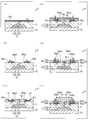
- FIG. 13F is a cross-sectional view showing a state where the organic semiconductor layer 16 is formed on the organic TFT 6 and the manufacture of the organic TFT 6 is completed.
- the organic TFT 6 includes a substrate 10, a first gate insulating layer 11, a second gate insulating layer 62, a gate electrode 13, a source electrode 64, a drain electrode 65, and an organic semiconductor layer 16.
- each member included in the organic TFT 6 of Embodiment 6 is the same as each member included in the organic TFT 1 of Embodiment 1 except for the second gate insulating layer 62, the source electrode 64, and the drain electrode 65. For this reason, the same member numbers are used.
- FIGS. 13A to 13F are cross-sectional views of the organic TFT 6, respectively, showing the respective steps in manufacturing the organic TFT 6.
- FIG. 10 is a diagram showing a step of forming a first layer base material 18a on the entire top surface of the first gate insulating layer 11 (first step in the sixth embodiment, step (d2)).
- the 1st process in Embodiment 6 is a process following the 3rd process in Embodiment 1 (refer to (c) of Drawing 2). That is, prior to the first step in the sixth embodiment, the first gate insulating layer 11 of the organic TFT 6 is the same as the first step (step (a1)) to the third step (step (c1)) in the first embodiment. A gate electrode 13 is formed on the substrate 10.
- One gate insulating layer 11 is formed.
- the gate electrode first layer 13a as the adhesion layer is formed to have a thickness of 5 nm
- the gate electrode second layer 13b as the contact layer is formed to have a thickness of 300 nm.
- a layer of a material functioning as an adhesion layer is formed on the entire upper surface of the first gate insulating layer 11 in the same manner as in the fourth step in the first embodiment (see FIG. 2D).
- the source / drain electrode first layer base material 18a is formed using a spin coater.
- Cr is selected as the material of the source / drain electrode first layer base material 18a
- FIG. 13B shows a step of forming the source electrode first layer 64a and the drain electrode first layer 65a from the source / drain electrode first layer base material 18a (second step and step (e2 in Embodiment 6)). )).
- the fifth step in the first embodiment is applied to the source / drain electrode first layer base material 18a covering the entire top surface of the first gate insulating layer 11. ) Is performed to remove unnecessary source / drain electrode first layer base material 18a and form source electrode first layer 64a and drain electrode first layer 65a.
- the source electrode first layer 64a and the drain electrode first layer 65a are formed apart from each other.
- the surface facing the drain electrode first layer 64b is referred to as a source electrode first layer side surface 64aS.
- the surface facing the source electrode first layer 64a is referred to as a drain electrode first layer side surface 65aS.
- FIG. 13C shows the first gate insulating layer 11 in the space between the source electrode first layer 64a and the drain electrode first layer 65a that are spaced apart from each other on the first gate insulating layer 11. It is a figure which shows the process (3rd process in Embodiment 6, process (f2)) which forms the 2nd gate insulating layer 62 located on the top.
- an insulating material is formed on the entire top surfaces of the first gate insulating layer 11, the source electrode first layer 64a, and the drain electrode first layer 65a using a spin coater.
- photolithography is performed to remove the insulating material film located on the upper surfaces of the source electrode first layer 64a and the drain electrode first layer 65a, and openings are formed on the upper surfaces of the source electrode first layer 64a and the drain electrode first layer 65a. A part 19 is formed.
- the second gate insulating layer 62 is formed in the space between the source electrode first layer 64a and the drain electrode first layer 65a.
- the second gate insulating layer 62 only needs to be formed so as to cover the entire source electrode first layer side surface 64aS and the entire drain electrode first layer side surface 65aS. Therefore, it is not necessary to form the second gate insulating layer 62 so as to satisfy d1 ⁇ d throughout the entire second gate insulating layer 62.
- the thickness of the second gate insulating layer 62 is larger than d1 in the portion in contact with the source electrode first layer 64a and the drain electrode first layer 65a, and the source electrode first layer 64a and the drain electrode first layer In a portion not in contact with 65a (for example, near the center of the second gate insulating layer 62), the number of film formation of the insulating material is reduced so that the film thickness of the second gate insulating layer 62 is smaller than d1.
- a second gate insulating layer 62 may be formed.
- the second gate insulating layer 62 according to the present embodiment has the same effect as the second gate insulating layer 52 in the fifth embodiment.
- FIG. 13D shows a step before forming (i) the source electrode second layer 64b included in the source electrode 64 and (ii) the drain electrode second layer 65b included in the drain electrode 65. It is a figure which shows the process (4th process in Embodiment 6, process (g2)) which forms the 2nd layer base material 18b in the whole upper surface of the 2nd gate insulating layer 62.
- a layer of a material that functions as a contact layer is formed on the entire top surfaces of the second gate insulating layer 62, the source electrode first layer 64a, and the drain electrode first layer 65a.
- the source / drain electrode second layer base material 18b is formed using a spin coater.
- Au is selected as the material of the source / drain electrode second layer base material 18b.
- FIG. 13E shows a step of forming the source electrode second layer 64b and the drain electrode second layer 65b from the source / drain electrode second layer base material 18b, and forming the source electrode 64 and the drain electrode 65 (see FIG. 13). It is a figure which shows the 5th process in Embodiment 6, a process (h2)).
- photolithography is performed on the source / drain electrode second layer base material 18b in the same manner as in the fifth step in the first embodiment (see FIG. 2E), and the source The source / drain electrode second layer base material 18b disposed at a position not corresponding to the opening 19 formed on the upper surfaces of the electrode first layer 64a and the drain electrode first layer 65a is removed.
- source / drain electrode second layer base materials 18b are left on the source electrode first layer 64a and the drain electrode first layer 65a so as to face each other.
- the remaining source / drain electrode second layer base material 18b becomes the source electrode second layer 64b and the drain electrode second layer 65b, respectively.
- the surface facing the drain electrode second layer 65b is referred to as a source electrode second layer side surface 64bS.
- the surface facing the source electrode second layer 64b is referred to as a drain electrode second layer side surface 65bS.
- a source electrode 64 having a source electrode first layer 64a and a source electrode second layer 64b, and (ii) a drain electrode 65 having a drain electrode first layer 65a and a drain electrode second layer 65b. are formed apart from each other.
- FIG. 13F shows the second gate insulating layer 62, the source so as to cover the entire surface of the second gate insulating layer 62, a part of the surface of the source electrode 64, and a part of the surface of the drain electrode 65. It is a figure which shows the process (6th process in Embodiment 6) which forms the organic-semiconductor layer 16 on the upper surface of the electrode 64 and the drain electrode 65.
- FIG. 13F shows the second gate insulating layer 62, the source so as to cover the entire surface of the second gate insulating layer 62, a part of the surface of the source electrode 64, and a part of the surface of the drain electrode 65.
- the sixth step in the sixth embodiment is a step corresponding to the seventh step in the first embodiment (see (g) in FIG. 2), and is the same as the seventh step (step (g1)) in the first embodiment.
- the organic semiconductor layer 16 is formed, and the manufacture of the organic TFT 6 of this embodiment is completed.
- the organic TFT 6 of the present embodiment is formed by the manufacturing steps from the first step to the sixth step described above in FIGS. 13A to 13F.
- FIG. 14B shows a manufacturing process for forming the second gate insulating layer 62 in the space between the source electrode first layer 64a and the drain electrode second layer 65a using a spin coater (Embodiment 6). It is a figure which shows the 3rd process in FIG.
- the organic TFT 6a is equivalent to the organic TFT according to any one of the first to fifth embodiments described above.
- the organic TFT 6a is equivalent to the organic TFT 1 of the first embodiment. Since each member with which organic TFT6a is provided is the same as that with which organic TFT1 of Embodiment 1 is provided, it shows using the same member number.
- FIG. 14A is a diagram corresponding to the third step in the sixth embodiment and is a diagram illustrating a manufacturing process for forming the second gate insulating layer by dropping the insulating material 56 using the inkjet 190. is there.
- FIG. 14 (a) is a diagram corresponding to FIG. 12 (a) showing the organic TFT 5a. Accordingly, the organic TFT 6a shown in FIG. 14A is similar to the organic TFT 5a in that the insulating material 56 dropped from the inkjet 190 a plurality of times is formed by the source electrode first layer 14a and the drain electrode first layer. It arrange
- the second gate insulating layer 62 is formed using a spin coater and photolithography as described in the third step of the sixth embodiment. A second gate insulating layer 62 is formed.
- the second gate insulating layer 62 of the organic TFT 6 is formed to have a more uniform film thickness than the second gate insulating layer of the organic TFT 6a. For this reason, the organic TFT 6 is realized as a device in which variation in characteristics is suppressed.
- FIG. 15 is a cross-sectional view of the organic TFT 7.
- the organic TFT 7 includes a substrate 10, a first gate insulating layer 11, a second gate insulating layer 72, a gate electrode 13, a source electrode 74, a drain electrode 75, and an organic semiconductor layer 16.
- each member included in the organic TFT 7 of Embodiment 7 is the same as each member included in the organic TFT 1 of Embodiment 1 except for the second gate insulating layer 72, the source electrode 74, and the drain electrode 75. For this reason, the same member numbers are used.
- the second gate insulating layer 72 of the organic TFT 7 is the same member as the second gate insulating layer 62 of the organic TFT 6 in the sixth embodiment.
- the source electrode 74 and the drain electrode 75 of this embodiment will be described.
- the source electrode 74 is an electrode formed in the same manner as the fifth step in Embodiment 6 (see FIG. 13E), (i) a source electrode first layer 74a that functions as an adhesion layer, and (Ii) A source electrode second layer 74b that functions as a contact layer is provided.
- the surface facing the drain electrode first layer 75a is referred to as a source electrode first layer side surface 74aS.
- the surface facing the source electrode first layer 74a is referred to as a drain electrode first layer side surface 75aS.
- the surface facing the drain electrode second layer 75b is referred to as a source electrode second layer side surface 74bS.
- a surface facing the source electrode second layer 74b is referred to as a drain electrode second layer side surface 75bS.
- the direction in which the source electrode 74 and the drain electrode 75 are opposed to each other is hereinafter referred to as a horizontal direction.
- a horizontal direction The direction in which the source electrode 74 and the drain electrode 75 are opposed to each other is hereinafter referred to as a horizontal direction.
- the end of the side surface opposite to the source electrode first layer side surface 74aS and the end of the side surface opposite to the source electrode second layer side surface 74bS are aligned in the horizontal direction. The case is illustrated.
- the source electrode first layer 74a and the source electrode second layer 74b are formed so that the above holds.
- drain electrode 75 is an electrode formed in the same manner as in the fifth step in Embodiment 6 (see FIG. 13E), (i) a drain electrode first layer 75a that functions as an adhesion layer, and (Ii) A drain electrode second layer 75b that functions as a contact layer is provided.
- drain electrode 75 As a magnitude relationship between the dimensions D1 and D2, D2> D1 (5)
- the drain electrode first layer 75a and the drain electrode second layer 75b are formed respectively.
- the end of the drain electrode second layer side surface 75bS is located closer to the source electrode 74 than the drain electrode first layer side surface 75aS. is doing. Therefore, the end of the drain electrode second layer side surface 75bS penetrates deeper into the organic semiconductor layer 16 than the end of the drain electrode first layer side surface 75aS.
- the horizontal distance between the source electrode first layer side surface 74aS and the drain electrode first layer side surface 75aS is expressed as a dimension SD1
- the distance between the source electrode second layer side surface 74bS and the drain electrode second layer side surface 75bS is shown.
- the horizontal distance between them is represented as dimension SD2.
- the dimension SD2 indicating the horizontal distance between the source electrode second layer side surface 74bS and the drain electrode second layer side surface 75bS is between the source electrode first layer side surface 74aS and the drain electrode first layer side surface 75aS. It is smaller than the dimension SD1 indicating the distance in the horizontal direction.
- FIG. 16B is a cross-sectional view of the organic TFT 7 of the present embodiment, and the gate voltage for controlling the channel of the organic semiconductor layer 16 provided in the organic TFT 7 is changed from the gate electrode second layer 13b of the gate electrode 13. It shows how it is given.
- the organic TFT 7a is equivalent to the organic TFT according to any one of the first to sixth embodiments.
- 16A is a cross-sectional view of the organic TFT 7a, and a gate voltage for controlling the channel of the organic semiconductor layer 16 included in the organic TFT 7a is given from the gate electrode second layer 13b of the gate electrode 13.
- FIG. It shows a state.
- the organic TFT 7a includes a second gate insulating layer 72, a source electrode 74c, and a drain electrode 75c.
- the source electrode 74c includes a source electrode first layer 74ca and a source electrode second layer 74cb.
- the drain electrode 75c includes a drain electrode first layer 75ca and a drain electrode second layer 75cb.
- a surface facing the drain electrode first layer 75ca is referred to as a source electrode first layer side surface 74caS.
- the surface facing the source electrode first layer 74ca is referred to as a drain electrode first layer side surface 75caS.
- the surface facing the drain electrode second layer 75b is referred to as a source electrode second layer side surface 74cbS.
- the surface facing the source electrode second layer 74cb is referred to as a drain electrode second layer side surface 75cbS.
- FIG. 16A the end of the side surface opposite to the source electrode first layer side surface 74caS and the end of the side surface opposite to the source electrode second layer side surface 74cbS are positioned in the horizontal direction. The case where these are mutually matched is illustrated.
- the source electrode first layer 74ca and the source electrode second layer 74cb are formed so that the above holds.
- FIG. 16A the end of the side surface opposite to the drain electrode first layer side surface 75caS and the end of the side surface opposite to the drain electrode second layer side surface 75cbS are positioned in the horizontal direction. The case where these are mutually matched is illustrated.
- drain electrode 75c As a magnitude relationship between the dimensions D1a and D2a, D1a> D2a (11)
- the drain electrode first layer 75ca and the drain electrode second layer 75cb are formed so that the above holds.
- the end of the drain electrode second layer side surface 75cbS is farther from the source electrode 74c than the drain electrode first layer side surface 75caS. positioned. Therefore, the end portion of the drain electrode second layer side surface 75cbS penetrates more shallowly into the organic semiconductor layer 16 than the end portion of the drain electrode first layer side surface 75caS.
- the horizontal distance between the source electrode first layer side surface 74caS and the drain electrode first layer side surface 75caS is expressed as a dimension SD1a
- the distance between the source electrode second layer side surface 74cbS and the drain electrode second layer side surface 75cbS is shown.
- the horizontal distance between them is represented as dimension SD2a.
- SD2a SD1a + (S2a1a + D2a1a) (13) Furthermore, from the equations (10) and (12), SD2a> SD1a (14) It becomes.
- the dimension SD2a indicating the horizontal distance between the source electrode second layer side surface 74cbS and the drain electrode second layer side surface 75cbS is between the source electrode first layer side surface 74caS and the drain electrode first layer side surface 75caS. It is larger than the dimension SD1a indicating the distance in the horizontal direction.
- the organic semiconductor layer 16 there is a channel formed in a region between the source electrode second layer side surface 74 cbS and the drain electrode second layer side surface 75 cbS.
- a gate voltage is applied from the gate electrode second layer 13b.
- the channel of the organic semiconductor layer 16 is controlled by the gate voltage, and the output characteristics of the organic TFT 7a are controlled by the gate voltage.
- the end of the source electrode second layer side surface 74cbS is more organic than the end of the source electrode first layer side surface 74caS.
- the end portion of the drain electrode second layer side surface 75cbS is shallower inside the organic semiconductor layer 16 than the end portion of the drain electrode first layer side surface 75caS. Invaded.
- the gate voltage applied to the channel of the organic semiconductor layer 16 from the gate electrode second layer 13b penetrates deeper into the organic semiconductor layer 16, (i) the end of the source electrode first layer side surface 74caS, And (ii) is blocked by the end of the drain electrode first layer side surface 75caS.
- the channel of the organic semiconductor layer 16 penetrates more shallowly into the organic semiconductor layer 16, (i) the end of the source electrode second layer side surface 74cbS, and (ii) the end of the drain electrode second layer side surface 75cbS. It is formed in the area between the parts.
- the channel formed in the organic semiconductor layer 16 has a wider range than the range in which the gate voltage can be applied from the gate electrode second layer 13b.
- the source electrode second layer side surface 74bS and the drain electrode second layer side surface 75bS are controlled by the gate voltage.
- the end portion of the source electrode second layer side surface 74bS is more organic than the end portion of the source electrode first layer side surface 74aS.
- the end portion of the drain electrode second layer side surface 75bS is deeper into the inside of the organic semiconductor layer 16 than the end portion of the drain electrode first layer side surface 75aS. Invaded.
- the gate voltage applied to the channel of the organic semiconductor layer 16 from the gate electrode second layer 13b penetrates deeper into the inside of the organic semiconductor layer 16, (i) the end portion of the side surface 74bS of the source electrode second layer, And (ii) is blocked by the end of the drain electrode second layer side surface 75bS.
- the channel of the organic semiconductor layer 16 also penetrates deeper into the organic semiconductor layer 16 (i) the end of the source electrode second layer side surface 74bS, and (ii) the drain electrode second layer side surface 75bS. It is formed in the region between the ends.
- the channel of the organic semiconductor layer 16 can be appropriately controlled by the gate voltage in the entire region between the source electrode second layer 74cb and the drain electrode second layer 75cb. Therefore, in the organic TFT 7, the controllability of the channel is further improved, and the reduction in output characteristics can be suppressed.
- the source electrode 74 and the drain electrode 75 may not include the source electrode first layer 74a and the drain electrode 74b as an adhesion layer, respectively. That is, each of the source electrode 74 and the drain electrode 75 may be composed of a plurality of conductive layers as in the embodiment 9 described later.
- the source electrode 74 and the drain electrode 75 are each composed of two conductive layers can be exemplified.
- the direction in which the source electrode and the drain electrode are opposed to each other is defined as a horizontal direction
- the surface on the side facing the drain electrode first layer in the source electrode first layer is defined as the side surface of the source electrode first layer.
- the surface facing the first source electrode layer is referred to as a drain electrode first layer side surface.
- the surface facing the drain electrode second layer is defined as the source electrode second layer side surface, and in the drain electrode second layer, the source electrode second layer is opposed.
- the surface on the other side is the side surface of the drain electrode second layer.
- the horizontal distance between the source electrode second layer side surface and the drain electrode second layer side surface is larger than the horizontal distance between the source electrode first layer side surface and the drain electrode first layer side surface. If it is made small, the same effect can be produced.
- FIG. 17D is a cross-sectional view showing a state where the organic semiconductor layer 16 is formed on the organic TFT 8 and the manufacture of the organic TFT 8 is completed.
- the organic TFT 8 includes a substrate 10, a first gate insulating layer 11, a second gate insulating layer 82, a gate electrode 13, a source electrode 84, a drain electrode 85, and an organic semiconductor layer 16.
- each member included in the organic TFT 8 of the eighth embodiment is the same as each member included in the organic TFT 1 of the first embodiment except for the second gate insulating layer 82, the source electrode 84, and the drain electrode 85. For this reason, the same member numbers are used.
- the second gate insulating layer 82 of the organic TFT 8 is the same member as the second gate insulating layer 72 of the organic TFT 7 in the seventh embodiment.
- the source electrode 84 includes a source electrode first layer 84a, a source electrode second layer 84b (source electrode intermediate layer), and a source electrode third layer 84c (source electrode second layer).
- FIGS. 17A to 17D are cross-sectional views of the organic TFT 8, and are diagrams showing respective steps in the manufacture of the organic TFT 8.
- FIG. 17A shows the first gate insulating layer 11 in the space between the source electrode first layer 84a and the drain electrode first layer 85a that are spaced apart from each other on the first gate insulating layer 11. It is a figure which shows the process (1st process in Embodiment 8) of forming the 2nd gate insulating layer 82 located on the top.
- the 1st process in Embodiment 8 is a process corresponding to the 3rd process in Embodiment 6 (refer to (c) of Drawing 13). That is, in the first step in the eighth embodiment, the first gate insulating layer 11, the gate electrode 13, the second gate insulating layer 82, and the source electrode first layer of the organic TFT 8 are performed in the same manner as in the third step in the sixth embodiment. 84 a and a drain electrode first layer 85 a are formed on the substrate 10. An opening 19 is formed on the upper surfaces of the source electrode first layer 84a and the drain electrode first layer 85a. Therefore, the second gate insulating layer 82 includes the opening 19.
- FIG. 17B shows a step of forming (i) a source electrode second layer 84b included in the source electrode 84 and (ii) a drain electrode second layer 85b included in the drain electrode 85 (second embodiment 8). It is a figure which shows a process.
- the source electrode second layer 84b is formed using a known electroplating technique so as to fill the opening 19 on the upper surface of the source electrode first layer 84a.
- the drain electrode second layer 85b is formed so as to fill the opening 19 on the upper surface of the drain electrode first layer 85a.
- Cu is selected as the material of the source electrode second layer 84b and the drain electrode second layer 85b.
- the source electrode second layer 84b and the drain electrode second layer 85b are used to reduce the amount of material used for the source electrode third layer 84c and the drain electrode third layer 85c for making contact with the organic semiconductor layer 16. This is an auxiliary conductive layer.
- the material of the source electrode second layer 84b and the drain electrode second layer 85b is not limited to Cu, and other conductive materials that are less expensive than the material of the source electrode third layer 84c and the drain electrode third layer 85c. May be used.
- FIG. 17C shows a step of forming (i) a source electrode third layer 84c included in the source electrode 84 and (ii) a drain electrode third layer 85c included in the drain electrode 85 (third in the eighth embodiment). It is a figure which shows a process.
- the source electrode third layer 84c is formed so as to cover the surface of the source electrode second layer 84b by using a plating method such as a known electroplating technique.
- the drain electrode third layer 85c is formed so as to cover the surface of the drain electrode second layer 85b.
- Au is selected as a material for the source electrode third layer 84c and the drain electrode third layer 85c, which can make good contact with the organic semiconductor layer 16.
- the source electrode third layer 84c and the drain electrode third layer 85c are thinner than the source electrode second layer 84b and the drain electrode second layer made of Cu in order to reduce the amount of Au used. Formed as a thin film.
- the source electrode 84 including the source electrode first layer 84a, the source electrode second layer 84b, and the source electrode third layer 84c
- the drain electrode first A drain electrode 85 including a first layer 85a, a drain electrode second layer 85b, and a drain electrode third layer 85c is formed.
- each of the source electrode 84 and the drain electrode 85 in a layer other than the uppermost layers of the source electrode 84 and the drain electrode 85 (that is, the source electrode third layer 84 c and the drain electrode third layer 85 c).
- a layer adjacent to the uppermost layer is formed so as to partially protrude from the opening 19 of the second gate insulating layer 82.
- each of the source electrode 84 and the drain electrode 85 covers (caps) the portion protruding from the second gate insulating layer 85 in the layer adjacent to the uppermost layer of each of the source electrode 84 and the drain electrode 85. )is doing.
- FIG. 17D shows the second gate insulating layer 82 and the source so as to cover the entire surface of the second gate insulating layer 82, a part of the surface of the source electrode 84, and a part of the surface of the drain electrode 85. It is a figure which shows the process (4th process in Embodiment 8) which forms the organic-semiconductor layer 16 on the upper surface of the electrode 84 and the drain electrode 85.
- the fourth step in the eighth embodiment is a step corresponding to the sixth step in the sixth embodiment, and is the same as the sixth step in the sixth embodiment, that is, the seventh step in the first embodiment (step (g1)).
- the organic semiconductor layer 16 is formed, and the manufacture of the organic TFT 8 of the present embodiment is completed.
- the organic TFT 8 of the present embodiment is formed by the manufacturing steps from the first step to the fourth step described above in FIGS. 17A to 17D.
- the second gate insulating layer 82 covers a part of the layers other than the uppermost layers of the source electrode 84 and the drain electrode 85 and has the opening 19. ing.
- the opening 19 provided in the second gate insulating layer 82 faces a layer other than the uppermost layer of each of the source electrode 84 and the drain electrode 85.
- the uppermost layers of the source electrode 84 and the drain electrode 85 are connected to layers other than the uppermost layers of the source electrode 84 and the drain electrode 85 through the opening 19 provided in the second gate insulating layer 82. Has been.
- the source electrode and the drain electrode are each formed using photolithography.
- the time and cost required for manufacturing the organic TFT 8 can be further reduced as compared with the organic TFTs of the first to seventh embodiments.
- the source electrode first made of Au is used to cover the surfaces of the source electrode second layer 84b and drain electrode second layer 85b made of Cu using a plating method.
- the third layer 84c and the third drain electrode layer 85c are formed, and the third source electrode layer 84c and the third drain electrode layer 85c are thinner than the second source electrode layer 84b and the second drain electrode layer 85b. It is formed as a thin film.
- the amount of Au used can be reduced by using a plating method compared to photolithography.
- the cost required for manufacturing the organic TFT 8 can be further reduced as compared with the organic TFTs of the first to seventh embodiments.
- FIG. 19D is a cross-sectional view showing a state where the organic semiconductor layer 16 is formed on the organic TFT 9 and the manufacture of the organic TFT 9 is completed.
- the organic TFT 9 includes a substrate 10, a first gate insulating layer 91, a second gate insulating layer 92, a gate electrode 13, a source electrode 94, a drain electrode 95, and an organic semiconductor layer 16.
- each member included in the organic TFT 9 of the ninth embodiment is the same as each member included in the organic TFT 1 of the first embodiment except for the second gate insulating layer 92, the source electrode 94, and the drain electrode 95. For this reason, the same member numbers are used.
- the first gate insulating layer 91 of the organic TFT 9 is the same member as the first gate insulating layer 81 of the organic TFT 8 in the eighth embodiment.
- the second gate insulating layer 92 of the organic TFT 9 is the same member as the second gate insulating layer 82 of the organic TFT 8 in the eighth embodiment.
- a surface treatment portion 91p including a source side surface treatment portion 91ps and a drain side surface treatment portion 91pd is formed.
- the source electrode 94 includes a source electrode first layer 94a (plating layer, in-opening plating layer, first plating layer), a source electrode second layer 94b (source electrode intermediate layer, second plating layer), and a source electrode third layer. 94c (surface plating layer), and the drain electrode 95 includes a drain electrode first layer 95a (plating layer, in-opening plating layer, first plating layer) and a drain electrode second layer 95b (drain electrode intermediate layer, first plating layer). 2 plating layers) and a drain electrode third layer 95c (surface plating layer).
- the source electrode first layer 94a is formed at a position on the first gate insulating layer 91 corresponding to the source side surface treatment portion 91ps, and the drain electrode first layer 95a is formed on the drain side surface treatment. It is formed at a position on the first gate insulating layer 91 corresponding to the portion 91pd.
- FIGS. 18A to 18E are cross-sectional views of the organic TFT 9, respectively, showing each step in the manufacture of the organic TFT 9.
- FIG. 18A shows a step of performing surface treatment on the first gate insulating layer 91 to form a surface treatment portion 91p including a source side surface treatment portion 91ps and a drain side surface treatment portion 91pd (Embodiment 9). It is a figure which shows the 1st process in (step (d3)).
- the first step in the ninth embodiment is a step following the third step in the first embodiment (see (c) in FIG. 2).
- the first gate insulating layer 91 of the organic TFT 9 is the same as the first step (step (a1)) to the third step (step (c1)) in the first embodiment.
- a gate electrode 13 is formed on the substrate 10.
- the second gate insulating layer 92 is formed on the upper surface of the first gate insulating layer 91.
- the second gate insulating layer 92 is patterned so that the openings 19 are provided on the upper surface of the first gate insulating layer 91 at positions corresponding to the source electrode 94 and the drain electrode 95, respectively.
- the pattern formation of the second gate insulating layer 92 may be performed by photolithography or may be performed by another printing technique.
- a known electroless plating technique for example, chemical plating
- a known electroless plating technique for example, chemical plating
- Surface treatment is performed so that it can be applied.
- the source side surface treatment portion 91ps is formed at a position corresponding to the source electrode 94, and (ii) the drain side surface treatment portion 91pd is formed. , Formed at a position corresponding to the drain electrode 95.
- polyimide containing fine particles of SiO 2 (silica, silicon dioxide) is used as the material of the first gate insulating layer 91, and fine particles of SiO 2 are used as the material of the second gate insulating layer 92.
- the polyimide which does not contain is used.
- the organic TFT 9 is impregnated with a strongly acidic aqueous solution such as HF (hydrogen fluoride) to thereby form SiO 2 positioned on the surface of the first gate insulating layer 91.
- a strongly acidic aqueous solution such as HF (hydrogen fluoride)
- the organic TFT 9 is impregnated with a solution containing palladium, so that the palladium flows into the holes on the surface of the first gate insulating layer 91. Since palladium functions as a catalyst for electroless plating, electroless plating can be selectively performed on the first gate insulating layer 91.
- the source-side surface treatment part 91ps and the drain-side surface treatment part 91pd that have been subjected to the surface treatment so as to enable electroless plating are formed.
- (Second step in Embodiment 9: source / drain electrode first layer forming step) 18B shows a step of (i) forming a source electrode first layer 94a included in the source electrode 94 and (ii) a drain electrode first layer 95a included in the drain electrode 95 (second embodiment 9). It is a figure which shows a process and a process (e3).
- the source electrode first layer 94a is formed using a known electroless plating technique so as to cover the upper surface of the source-side surface treatment portion 91ps.
- the drain electrode first layer 95a is formed so as to cover the upper surface of the drain-side surface treatment portion 91pd.
- the source electrode first layer 94a and the drain electrode first layer 95a function as an adhesion layer for the source electrode 94 and the drain electrode 95, respectively.
- Ni is selected as the material of the source electrode first layer 94a and the drain electrode first layer 95a.
- the first plating solution 96a made of Ni for the organic TFT 9 (i) the upper surface of the source-side surface treatment portion 91ps subjected to the surface treatment, and (ii) the surface treatment is performed.
- the first plating solution 96a adheres to the upper surface of the drain-side surface treatment portion 91pd.
- the source electrode first layer 94a and the drain electrode first layer 95a are formed.
- the source-side surface treatment part 91ps and the drain-side surface treatment part 91pd formed in the first step in Embodiment 9 have strong adhesion to metal. That is, the source-side surface treatment portion 91ps and the drain-side surface treatment portion 91pd can function as an adhesion layer as an alternative to the source electrode first layer 94a and the drain electrode first layer 95a as the adhesion layer.
- the second step in the ninth embodiment is omitted, and in the third step described later, the source-side surface treatment unit 91ps and the drain that serve as the adhesion layer are used as the source electrode second layer 94b and the drain electrode second layer 95b, respectively. You may form so that the upper surface of the side surface treatment part 91pd may be coat
- FIG. 18C shows a step of (i) forming a source electrode second layer 94b included in the source electrode 94, and (ii) a drain electrode second layer 95b included in the drain electrode 95 (third in the ninth embodiment). It is a figure which shows a process and a process (f3).
- the third step in the ninth embodiment is the same as the second step in the eighth embodiment, and the source electrode second layer 94b and the drain electrode second layer 95b are respectively formed using a known electroplating technique.
- Cu is selected as the material of the source electrode second layer 94b and the drain electrode second layer 95b.
- the second plating solution 96b made of Cu for the organic TFT 9 (i) on the upper surface of the source electrode first layer 94a and (ii) on the upper surface of the drain electrode first layer 95a, 2 plating solutions 96b adhere to each other. In this manner, the source electrode second layer 94b and the drain electrode second layer 95b are formed.
- the source electrode second layer 94b and the drain electrode second layer 95b are auxiliary conductive layers for the source electrode 94 and the drain electrode 95 provided to reduce the contact resistance of the electrode.
- (Fourth step in the ninth embodiment: source / drain electrode third layer forming step) 18D shows a step of forming (i) a source electrode third layer 94c included in the source electrode 94, and (ii) a drain electrode third layer 95c included in the drain electrode 95 (fourth embodiment 9). It is a figure which shows a process and a process (g3).
- the fourth step in the ninth embodiment is the same as the third step in the eighth embodiment, and the source electrode third layer 94c and the drain electrode third layer 95c are formed by using a known electroplating technique.
- Au is selected as the material for the source electrode third layer 94c and the drain electrode third layer 95c.
- the third plating solution 96c made of Au for the organic TFT 9 (i) on the upper surface of the source electrode second layer 94b and (ii) on the upper surface of the drain electrode second layer 95b, Three plating solutions 96c adhere to each other. Thus, the source electrode third layer 94c and the drain electrode third layer 95c are formed.
- the third source electrode layer 94 c and the third drain electrode layer 95 c are the main conductive layers of the source electrode 94 and the drain electrode 95 provided to make good contact with the organic semiconductor layer 16.
- FIG. 18E shows the second gate insulating layer 92, the source so as to cover the entire surface of the second gate insulating layer 92, a part of the surface of the source electrode 94, and a part of the surface of the drain electrode 95. It is a figure which shows the process (5th process in Embodiment 9) which forms the organic-semiconductor layer 16 on the upper surface of the electrode 94 and the drain electrode 95.
- FIG. 18E shows the second gate insulating layer 92, the source so as to cover the entire surface of the second gate insulating layer 92, a part of the surface of the source electrode 94, and a part of the surface of the drain electrode 95.
- the fifth step in the ninth embodiment is a step corresponding to the fourth step in the eighth embodiment, and is the same as the fourth step in the eighth embodiment, that is, the seventh step in the first embodiment (step (g1)).
- the organic semiconductor layer 16 is formed, and the manufacture of the organic TFT 9 of this embodiment is completed.
- the source electrode second layer 84b and the source electrode third layer 84c, and (ii) the drain electrode second layer 85b and the drain electrode third layer 95c are plated. Is formed by.
- the source electrode first layer 84a and the drain electrode first layer 85a as the adhesion layers are formed using photolithography.
- the source electrode first layer 94a and the drain electrode first layer 95a as the adhesion layers are also formed by using a plating method. In this respect, unlike the organic TFT 8 of the eighth embodiment. Yes.
- the organic TFT 9 of the present embodiment is manufactured without using the photolithography that requires a large number of steps for the source electrode first layer 94a and the drain electrode first layer 95a as the adhesion layers. Compared with the TFT 8, it is possible to further reduce the time and cost required for manufacturing.
- the source electrode 94 and the drain electrode 95 do not include the source electrode first layer 94a and the drain electrode first layer 95a as the adhesion layers, respectively, and the source electrode first layer as the auxiliary conductive layer is included.
- the two layers 94b and the drain electrode second layer 95b may be formed of a plurality of layers.
- the second gate insulating layer 92 has a total thickness of layers other than the uppermost layer of the source electrode 94 (ie, the source electrode third layer 94c), and other than the uppermost layer of the drain electrode (drain electrode third layer 95c).
- the total thickness of the layers may be larger than the total thickness of the source electrode 94 and the entire thickness of the drain electrode 95.
- the uppermost layers (that is, the source electrode third layer 94 c and the drain electrode third layer 95 c) of the source electrode 94 and the drain electrode 95 are connected via the opening 19 provided in the second gate insulating layer.
- the source electrode 94 and the drain electrode 95 are connected to layers other than the uppermost layer.
- the source electrode first layer 94a and the drain electrode first layer 95a as the adhesion layer described above are not included, and the source electrode second layer 94b and the drain electrode second layer 95b as the auxiliary conductive layers are a plurality of layers. Also in the structure formed from, the same effect can be produced by providing the same structure.
- the semiconductor element (organic TFT 1) includes the gate electrode (13), the first gate insulating layer (11) covering the gate electrode, and the first gate insulating layer in plan view.
- a source electrode (14) and a drain electrode (15) that are spaced apart from each other with the gate electrode interposed therebetween and overlap with a part of the gate electrode via the first gate insulating layer, and on the first gate insulating layer
- a second gate insulating layer (12) formed at least in a region sandwiched between the source electrode and the drain electrode, between the source electrode and the drain electrode, and on the source electrode and the drain electrode,
- the source electrode and the gate electrode are composed of a plurality of layers, and the uppermost layer of each of the source electrode and the drain electrode is made of a material of the semiconductor layer rather than the material of the layers other than the uppermost layer of the source
- the source electrode and the drain electrode are in direct contact with the semiconductor layer on the upper surface and side surfaces of the respective uppermost layers, and the uppermost layer of the source and drain electrodes is made of a material having a small work function. Between the other layers and the semiconductor layer, at least one of the second gate insulating layer and the uppermost layer of the source electrode and the drain electrode is interposed.
- a current flows through an interface portion between the semiconductor layer and the gate insulating layer, which is located between the source electrode and the drain electrode.
- the source electrode and the drain electrode are formed of a plurality of layers, there is a layer that cannot make good contact with the semiconductor layer in the source electrode and the drain electrode at the interface portion between the semiconductor layer and the gate insulating layer.
- the contact resistance increases and the characteristics of the semiconductor element deteriorate.
- the contact resistance of the source electrode and the drain electrode increases as a material having a large difference from the work function of the material of the semiconductor layer is used for the source electrode and the drain electrode. For this reason, as a material of a source electrode and a drain electrode, it is so preferable that the difference with the work function of the material of a semiconductor layer is small.
- a material of a source electrode and a drain electrode it is so preferable that the difference with the work function of the material of a semiconductor layer is small.
- Such a material generally includes, for example, gold. However, such materials are expensive.
- the source electrode and the drain electrode include a layer having higher adhesion (wetability) with the gate electrode than the layer as an adhesion layer with the gate electrode. Preferably it is.
- the second gate insulating film functions as a part of the gate insulating film.
- the second gate insulating layer and the uppermost layer of the source electrode and the drain electrode are disposed between the semiconductor layer and a layer other than the uppermost layer of the source electrode and the drain electrode. At least one of the upper layers is interposed.
- the semiconductor layer is not in direct contact with the layers other than the uppermost layers of the source electrode and the drain electrode.
- the semiconductor layer is in direct contact with the uppermost layers of the source electrode and the drain electrode. Therefore, the semiconductor layer can make good electrical contact with the uppermost layer of each of the source electrode and the drain electrode having a work function value closer to its own work function value.
- the semiconductor layer is not in direct contact with the layers other than the uppermost layers of the source electrode and the drain electrode. Therefore, it is possible to suppress electrical contact between the semiconductor layer and a layer other than the uppermost layer of each of the source electrode and the drain electrode having a work function value different from its own work function value. Can do.
- the source electrode and the gate electrode are in close contact with the first gate insulating layer (for example, the source electrode first layer 14a and the drain electrode, respectively).
- the second gate insulating layer includes at least the thickness of the adhesion layer (for example, d1), and the total thickness of the source electrode and the entire thickness of the drain electrode (for example, the first layer 15a). , D1 + d2) may be formed thinner.
- At least a part of the side surface of at least the uppermost layer of the source electrode and the drain electrode in the region sandwiched between the source electrode and the drain electrode is not covered with the second gate insulating layer.
- the side surface of the adhesion layer is covered with a second gate insulating layer so as not to be in direct contact with the semiconductor layer.
- the second gate insulating layer can suppress electrical contact between the semiconductor layer and the adhesion layer of the source electrode and the drain electrode, and the uppermost layer of each of the source electrode and the drain electrode. Electrically good contact can be made between the semiconductor layer and the semiconductor layer.
- the semiconductor element according to aspect 3 of the present invention is the semiconductor element according to aspect 1 or 2, wherein the second gate insulating layer has a total thickness other than the uppermost layer of the source electrode and other than the uppermost layer of the drain electrode.
- the total thickness of the layers may be larger than the total thickness of the source electrode and the drain electrode.
- the side surface of the uppermost layer of the source electrode and the drain electrode in the region sandwiched between the source electrode and the drain electrode is not covered with the second gate insulating layer.
- Side surfaces of layers other than the uppermost layer of the gate electrode are covered with a second gate insulating layer so as not to be in direct contact with the semiconductor layer.
- the second gate insulating layer can suppress electrical contact between the semiconductor layer and a layer other than the uppermost layer of the source electrode and the gate electrode, and each of the source electrode and the drain electrode can be suppressed. Good electrical contact can be made between the uppermost layer and the semiconductor layer.
- the semiconductor element according to aspect 4 of the present invention is the semiconductor element according to aspect 1, wherein the source electrode and the gate electrode are in close contact with the first gate insulating layer (for example, the source electrode first layer 14a and the drain electrode, respectively).
- the first layer 15a) and the uppermost layer for example, the source electrode second layer 14b and the drain electrode second layer 15b
- the second gate insulating layer is sandwiched between the source electrode and the drain electrode.
- the source-side second gate insulating layer (52a) covering the side surface (for example, the source electrode first layer side surface 14aS) of the source electrode in the closed region
- a drain-side second gate insulating layer (52b) covering a side surface of the adhesion layer of the drain electrode (for example, the drain electrode first layer side surface 15aS)
- the second gate insulating layer and the drain-side second gate insulating layer may have a structure provided separately from each other.
- the structure can suppress that an electrical contact arises in a semiconductor layer and an adhesion layer by a source side 2nd gate insulating layer and a drain side 2nd gate insulating layer 2nd gate insulating layer. At the same time, good electrical contact can be made between the uppermost layer of each of the source electrode and the drain electrode and the semiconductor layer.
- the portion where the source-side second gate insulating layer and the drain-side second gate insulating layer are not in contact for example, the central portion in the region sandwiched between the source electrode and the drain electrode. Only the uniform first gate insulating layer exists as the gate insulating layer. For this reason, compared with the case where the 2nd gate insulating layer is formed in the whole area
- the semiconductor element according to aspect 5 of the present invention is the semiconductor element according to aspect 1 or 2, wherein the second gate insulating layer is the source electrode and drain electrode in a layer other than the uppermost layer of the source electrode and drain electrode.
- the structure which covers the whole surface which is not in contact with each uppermost layer may be sufficient.
- the uppermost layer of each of the source electrode and the drain electrode is connected to a layer other than the uppermost layer of each of the source electrode and the drain electrode (for example, in the opening (19) of the second gate insulating layer). Even if the source electrode second layer 14b and the drain electrode second layer 15b) are partially in contact with each other, the layers other than the uppermost layers of the source electrode and the drain electrode are The entire surface of the source electrode and drain electrode that is not in contact with the uppermost layer is covered with the second gate insulating layer. According to the above configuration, the second gate insulating layer also covers the side surfaces of the layers other than the uppermost layers of the source electrode and the drain electrode on the side opposite to the region sandwiched between the source electrode and the drain electrode. Yes.
- the second gate insulating layer can suppress electrical contact between the semiconductor layer and a layer other than the source electrode and the uppermost layer of the gate electrode, and the source. Good electrical contact can be made between the uppermost layer of each of the electrode and drain electrode and the semiconductor layer.
- the above configuration can be easily realized by, for example, photolithography without using the ink jet method.
- the semiconductor element according to Aspect 6 of the present invention is the semiconductor element according to Aspect 5, wherein the second gate insulating layer covers a part of the layers other than the uppermost layers of the source electrode and the drain electrode. Openings (19) facing layers other than the uppermost layers of the source electrode and the drain electrode are provided, and the uppermost layers of the source electrode and the drain electrode are provided in the second gate insulating layer. It may be configured to be connected to a layer other than the uppermost layers of the source electrode and the drain electrode (for example, the source electrode first layer 14a and the drain electrode first layer 15a) through the opening.
- the above configuration enables formation of the second gate insulating layer using pattern formation by photolithography. Therefore, according to the above configuration, the thickness and shape of the second gate insulating film can be accurately controlled, and the distribution and fluctuation of the characteristics of the semiconductor element can be reduced.
- a source electrode and a drain electrode having a plurality of layers can be easily formed.
- the semiconductor device according to aspect 7 of the present invention is the semiconductor element according to aspect 6, which is opposed to each other in the uppermost layers (for example, the source electrode second layer 14 b and the drain electrode second layer 15 b) of the source electrode and the drain electrode.
- the end on the side is closer to the source than the end on the side facing each other in the layers other than the uppermost layers of the source electrode and the drain electrode (for example, the source electrode first layer 14a and the drain electrode first layer 15a).
- interposed by the electrode and the drain electrode may be sufficient.
- the source located inside the region sandwiched between the source electrode and the drain electrode.
- a channel of the semiconductor layer is formed in a region between the opposite end portions of the uppermost layer of each of the electrode and the drain electrode. Then, a gate voltage from the gate electrode for controlling the channel is applied to the same region described above.
- the second gate insulating layer is formed thinner than a total thickness of the layers other than the uppermost layers of the source electrode and the drain electrode. And a layer adjacent to the uppermost layer of the source electrode and the drain electrode in a layer other than the uppermost layer of the source electrode and the drain electrode is an opening of the second gate insulating layer.
- the uppermost layer of each of the source electrode and the drain electrode protrudes from the second gate insulating layer in a layer adjacent to the uppermost layer of the source electrode and the drain electrode.
- the above configuration enables formation of the second gate insulating layer using pattern formation by photolithography. Therefore, according to the above configuration, the thickness and shape of the second gate insulating film can be accurately controlled, and the distribution and fluctuation of the characteristics of the semiconductor element can be reduced.
- the portion of the layer adjacent to the uppermost layer of the source electrode and the drain electrode that protrudes from the second gate insulating layer is the uppermost layer of the source electrode and the drain electrode.
- the second gate insulating layer, the source electrode and the drain are disposed between the semiconductor layer and the layer other than the uppermost layer of the source electrode and the drain electrode in the region sandwiched between the source electrode and the drain electrode.
- the uppermost layer of the electrode can be easily interposed.
- the state which only the uppermost layer of the source electrode and the drain electrode exposed from the 2nd gate insulating layer can be produced easily.
- the semiconductor element according to aspect 9 of the present invention is the semiconductor element according to aspect 8, wherein at least a layer adjacent to the uppermost layer of each of the source electrode and the drain electrode in a layer other than the uppermost layer of each of the source electrode and the drain electrode.
- the structure may be an electroless plating layer.
- At least the layer adjacent to the uppermost layer of each of the source electrode and the drain electrode can be formed by electroless plating, and the manufacture of the source electrode and the drain electrode is simplified. Can do.
- the semiconductor element according to aspect 10 of the present invention is the semiconductor element according to aspect 9, wherein an electroless plating catalyst is selectively attached to a contact surface of the first gate insulating layer with the source electrode and the drain electrode. It may be a configuration.
- the first gate insulating layer is made of polyimide, and pores to which palladium, which is an electroless plating catalyst, is selectively formed on the contact surface of the first gate insulating layer with the source electrode and the drain electrode. It may be configured.
- layers other than the uppermost layers of the source electrode and the drain electrode can be formed in the opening by only electroless plating. For this reason, the cost concerning manufacture of a semiconductor element can be reduced.
- the contact surface of the first gate insulating layer with the source electrode and the drain electrode functions as an adhesion layer with the source electrode and the drain electrode, so the first gate insulating layer, the source electrode, and the drain.
- the source electrode and the gate electrode are each composed of three layers, and each of the source electrode and the drain electrode
- the intermediate layer (intermediate layer adjacent to the uppermost layer of each of the source electrode and the drain electrode) has a difference in work function of the material of the semiconductor layer from the material of the lowermost layer of the source electrode and the drain electrode.
- the structure may be made of a material having a work function that is small and has a larger difference from the work function of the material of the semiconductor layer than the material of the uppermost layer of the source electrode and the drain electrode.
- metals such as gold used for the uppermost layer are very expensive, and it is desirable to reduce the amount of use. According to said structure, while the usage-amount of the material used for the said uppermost layer can be reduced, the contact resistance of a source electrode and a drain electrode can be reduced by the said intermediate
- the semiconductor element according to Aspect 12 of the present invention is the semiconductor element according to any one of Aspects 1 to 11, wherein the dielectric constant value ( ⁇ 2 ) of the second gate insulating layer is the dielectric constant of the first gate insulating layer.
- the configuration may be smaller than the value of rate ( ⁇ 1 ).
- the characteristic of a semiconductor element can be improved.
- the value of the dielectric constant of the first gate insulating layer is reduced to the value of the dielectric constant of the second gate insulating layer.
- the film thickness at which the same capacity can be obtained can be increased.
- the leakage current and the breakdown voltage of the semiconductor element can be improved.
- the semiconductor element according to aspect 13 of the present invention is the semiconductor device according to any one of the aspects 1 to 12, wherein the first gate insulating layer and the second gate insulating layer have different surface energies. It may be.
- the surface energy value of the second gate insulating layer larger than the surface energy value of the first gate insulating layer, it is possible to improve the manufacturing accuracy of the semiconductor element.
- the characteristics of the semiconductor element can be improved by making the surface energy value of the second gate insulating layer smaller than the surface energy value of the first gate insulating layer.
- the surface energy value (ES2) of the second gate insulating layer is greater than the surface energy value (ES1) of the first gate insulating layer.
- a large configuration may be used.
- the manufacturing accuracy of the semiconductor element can be improved.
- the surface energy value of the second gate insulating layer in the aspect 13 may be smaller than the surface energy value of the first gate insulating layer. Good.
- the characteristics of the semiconductor element can be improved.
- the semiconductor element according to aspect 16 of the present invention may be configured such that in any one of the above aspects 1 to 15, the semiconductor layer is an organic semiconductor layer.
- the above-described configuration is particularly suitable when the semiconductor is an organic semiconductor.
- a method for manufacturing a semiconductor device includes: a first gate insulating layer forming step of forming a first gate insulating layer that covers a gate electrode; and the first gate insulating layer on the first gate insulating layer in plan view.
- the second gate insulating layer is added to the region sandwiched between the source electrode and the drain electrode on the first gate insulating layer, and the total of the layers other than the uppermost layer of the source electrode. And the total thickness of the layers other than the uppermost layer of the drain electrode, and the total thickness of the source electrode and the drain electrode It is characterized in that thinner than the thickness of the body.
- a method for manufacturing a semiconductor device includes a first gate insulating layer forming step of forming a first gate insulating layer covering a gate electrode, and the above-described method in plan view on the first gate insulating layer.
- the source-side second gate insulating layer and the drain-side second gate insulating layer so that at least part of the side surface of the source electrode second layer and at least part of the side surface of the drain electrode second layer are exposed in the region. It is characterized by forming.
- the second gate insulating layer in the Aspect 17 or 18, in the second gate insulating layer forming step, the second gate insulating layer may be formed by an inkjet method. Good.
- the second gate insulating layer can be formed only in a necessary portion.
- a method for manufacturing a semiconductor device includes a first gate insulating layer forming step of forming a first gate insulating layer covering a gate electrode, and the above-described method in plan view on the first gate insulating layer.
- Source electrode first layer / drain forming a source electrode first layer and a drain electrode first layer which are spaced apart from each other with the gate electrode interposed therebetween and overlap with a part of the gate electrode via the first gate insulating layer, respectively.
- the gate electrode is connected to the first layer of the source electrode through the opening to be exposed and spaced apart from each other with the gate electrode interposed therebetween in plan view, and the gate through the first gate insulating layer and the source electrode first layer.
- Source electrode second layer overlapping a part of the electrode, and the drain electrode through the opening exposing the drain electrode first layer of the opening on the second gate insulating layer;
- a drain electrode connected to the first layer and spaced apart from each other across the gate electrode in plan view and overlapping a part of the gate electrode via the first gate insulating layer and the drain electrode first layer
- Source electrode second layer / drain electrode second layer forming step for patterning two layers, source electrode second layer and drain electrode second layer, and source electrode second layer
- the second gate insulating layer can be formed using pattern formation by photolithography. Therefore, according to the above configuration, the film thickness and shape of the second gate insulating film can be accurately controlled, and the distribution and fluctuation of characteristics of the obtained semiconductor element can be reduced.
- the source electrode second layer and the drain electrode second layer are formed in the source electrode second layer / drain electrode second layer forming step.
- the end portions of the source electrode second layer and the drain electrode second layer that face each other are closer to the source electrode first layer than the end portions of the source electrode first layer and the drain electrode first layer that face each other. Even if it is formed so as to protrude inside a region sandwiched between the source electrode composed of one layer and the second source electrode layer and the drain electrode composed of the first drain electrode layer and the second drain electrode layer. Good.
- the inner side of the region sandwiched between the source electrode and the drain electrode A channel of the semiconductor layer is formed in a region between the opposite end portions of the uppermost layer of each of the source electrode and the drain electrode, which is located in (1). Then, a gate voltage from the gate electrode for controlling the channel is applied to the same region described above.
- the controllability of the channel of the semiconductor layer is improved. It is possible to provide a semiconductor element that can suppress deterioration in characteristics of the semiconductor element.
- a method for manufacturing a semiconductor device includes a first gate insulating layer forming step of forming a first gate insulating layer that covers a gate electrode, and the above-described method in plan view on the first gate insulating layer.
- a second gate insulating layer having an opening exposing the first gate insulating layer in a region that is separated from each other with the gate electrode interposed therebetween and overlaps with a part of the gate electrode via the first gate insulating layer.
- the plating layer in the opening for example, the source electrode first layer 94a and the drain electrode first layer 95a
- the surface plating layer used as a part of the source electrode and the drain electrode by electroless plating Therefore, the production of the source electrode and the drain electrode can be simplified, and the cost for manufacturing the semiconductor element can be reduced.
- a method for manufacturing a semiconductor device is the method for manufacturing a semiconductor element according to aspect 22, wherein the source electrode and the drain electrode are formed on the first gate insulating layer before the second gate insulating layer forming step.
- the adhesion layer used as a portion and the first gate insulating layer is separated from each other with the gate electrode interposed therebetween in a plan view, and overlaps with a part of the gate electrode via the first gate insulating layer. And forming a pattern so that a part of the upper surface of the adhesion layer is exposed in the opening.
- the plating layer is formed on the adhesion layer exposed from the opening, and in the adhesion layer formation step, the above-described adhesion layer is formed on the adhesion layer.
- the plated layer formed by the mouth portion in the plating layer forming step may be configured to use a material having a work function difference is large between the work function of the material of the semiconductor layer.
- metals such as gold used for the uppermost layer are very expensive, and it is desirable to reduce the amount of use. According to said structure, while the usage-amount of the material used for the said uppermost layer can be reduced, the contact resistance of a source electrode and a drain electrode can be reduced by the said intermediate
- the method for manufacturing a semiconductor device according to aspect 24 of the present invention is the method for manufacturing a semiconductor element according to aspect 22, wherein the electroless plating catalyst is formed on the surface of the first gate insulating layer in the opening before the in-opening plating layer forming step.
- the structure which has the process of making it adhere may be sufficient.
- the plating layer in the opening and the surface plating layer can be formed in the opening only by electroless plating. For this reason, the cost concerning manufacture of a semiconductor element can be reduced.
- the contact surface of the first gate insulating layer with the source electrode and the drain electrode functions as an adhesion layer with the source electrode and the drain electrode, so the first gate insulating layer, the source electrode, and the drain.
- an adhesion layer with the first gate insulating layer is not necessarily formed on the source electrode and drain electrode sides in order to improve adhesion with the electrode.
- the in-opening plating layer forming step includes an electroless plating in the opening to form an adhesion layer with the first gate insulating layer.
- a first plating layer forming step of forming a first plating layer for example, a source electrode first layer 94a and a drain electrode first layer 95a
- a second plating layer for example, a source electrode second layer 94b
- the semiconductor element according to one embodiment of the present invention can be manufactured by the above-described method for manufacturing a semiconductor element.
- a semiconductor element that includes a source electrode and a drain electrode composed of three layers and suppresses deterioration in characteristics, and has no source electrode and drain electrode composed of three layers. It can be formed only by electrolytic plating.
- metals such as gold used for the uppermost layer are very expensive, and it is desirable to reduce the amount of use. According to said structure, while the usage-amount of the material used for the said uppermost layer can be reduced, the contact resistance of a source electrode and a drain electrode can be reduced by the said intermediate
- the method for manufacturing a semiconductor device according to aspect 26 of the present invention may be configured such that, in any one of the above aspects 17 to 25, the semiconductor layer is formed by an inkjet method in the semiconductor layer forming step. .
- the method for manufacturing a semiconductor device according to aspect 27 of the present invention may be configured such that, in any one of the above aspects 17 to 25, the semiconductor is formed by a spin coating method in the semiconductor layer forming step. .
- the method for manufacturing a semiconductor device according to aspect 28 of the present invention is the method for manufacturing a semiconductor element according to any one of the above aspects 17 to 27, wherein in the second gate insulating layer forming step, the material of the second gate insulating layer is used as the second gate insulating layer.
- a structure using a material having a dielectric constant smaller than the value of the dielectric constant of one gate insulating layer may be used.
- the characteristics of the obtained semiconductor element can be improved.
- the value of the dielectric constant of the first gate insulating layer is reduced to the value of the dielectric constant of the second gate insulating layer.
- the film thickness at which the same capacity can be obtained can be increased.
- the leakage current and the breakdown voltage of the semiconductor element can be improved.
- the surface energy of the first gate insulating layer is used as the material of the second gate insulating layer.
- the structure using the material which has a surface energy larger than the value of may be sufficient.
- the manufacturing accuracy of the semiconductor element can be improved.
- the surface energy of the first gate insulating layer is used as the material of the second gate insulating layer.
- the structure which uses the material which has surface energy smaller than the value of may be sufficient.
- the characteristics of the obtained semiconductor element can be improved.
- a method for manufacturing a semiconductor device is the method for manufacturing a semiconductor element according to aspect 26, wherein the second gate insulating layer obtained in the second gate insulating layer forming step is applied to the second gate insulating layer before the semiconductor layer forming step.
- the structure may further include a surface treatment step of performing a surface treatment for making the surface energy of the second gate insulating layer larger than the value of the surface energy of the first gate insulating layer.
- the semiconductor element according to one embodiment of the present invention can be manufactured by the above-described method for manufacturing a semiconductor element.
- the manufacturing accuracy of the semiconductor element can be improved.
- a method for manufacturing a semiconductor device according to aspect 32 of the present invention is the method for manufacturing a semiconductor element according to aspect 27, wherein the first gate insulating layer is formed between the first gate insulating layer forming step and the second gate insulating layer forming step.
- the characteristics of the obtained semiconductor element can be improved.
- the semiconductor element manufacturing method according to Aspect 33 of the present invention may be configured such that, in the Aspect 31 or 32, the surface treatment is ultraviolet light irradiation.
- the surface treatment may be a coating of a monomolecular film of a silane coupling agent.
- the present invention can also be expressed as follows.
- the semiconductor element of the present invention is an element using an organic semiconductor layer
- the source / drain electrode is composed of two or more layers
- the gate insulating film occupies most of the substrate.
- the insulating film and at least a second insulating film formed in the channel region of the transistor, and the second insulating film is the uppermost layer of the source / drain electrode capable of forming a good contact with the organic semiconductor layer.
- the other electrode surface is covered so as not to contact the organic semiconductor layer.
- the second insulating film is thicker than the first source / drain electrode (adhesion layer) in contact with the first insulating film and thinner than the entire thickness of the source / drain electrode. .
- the second insulating film has a dielectric constant smaller than that of the first insulating film.
- the surface energy is different between the first insulating film and the second insulating film.
- the first insulating film is subjected to a material or surface treatment capable of electroless plating
- the second insulating film is subjected to a material or surface treatment not subjected to electroless plating.
- the source / drain electrode after the pattern of the second insulating film is formed, at least the first layer is formed by electroless plating.
- the present invention can be used for a semiconductor element and a method for manufacturing a semiconductor element.
Landscapes
- Engineering & Computer Science (AREA)
- Manufacturing & Machinery (AREA)
- Thin Film Transistor (AREA)
Abstract
有機TFT(1)のソース電極(14)およびドレイン電極(15)のそれぞれの最上層(14b,15b)の材料は、最上層以外の層(14a,14b)の材料よりも半導体層(16)の材料の仕事関数との差が小さい。ソース電極(14)およびドレイン電極(15)は、それぞれの最上層の上面および側面で半導体層(16)と直接接触し、最上層以外の層と半導体層(16)との間には、第2ゲート絶縁層(12)が介在している。
Description
本発明は、半導体素子、および半導体素子の製造方法に関する。
近年、次世代のトランジスタ技術として、有機半導体層を用いたTFT(Thin Film Transistor,薄膜トランジスタ)が注目されている。
有機TFTは、100℃から200℃まで程度の低温のプロセスによって製造することが可能であるため、プラスチック基板上に直接的に形成することができる。また、有機TFTは、半導体層および絶縁層がともに有機材料によって形成されているため、曲げに対する耐性が強く、フィルム液晶および電子ペーパ等のフレキシブルディスプレイへの応用が期待されている。
有機TFTの一般的な構造としては、ボトムゲート・ボトムコンタクト構造が広く適用されている。ボトムゲート・ボトムコンタクト構造では、ゲート電極およびゲート絶縁層が基板上に形成され、続いて、ゲート絶縁層の上にソース電極およびドレイン電極が形成される。その後、ゲート絶縁層、ソース電極、およびドレイン電極の上に、有機半導体が形成される。
研究段階においては、有機TFTにおけるソース電極およびドレイン電極の材料として、有機半導体層との良好なコンタクトを取ることが可能な金属である金が用いられ、ソース電極およびドレイン電極は、Au(金)の単層膜として形成されることが一般的である。
ボトムゲート構造の有機TFTにおいては、ソース電極とドレイン電極との間に位置する、有機半導体層とゲート絶縁層との界面近傍の領域において、有機半導体のチャネルが形成され、有機半導体における電流はチャネル内を流れることができる。
特許文献1には、ソース電極とドレイン電極との間にゲート絶縁層をさらに設け、有機半導体層を平坦化させる平坦化層とすることにより、有機半導体のチャネルを移動するキャリアの移動度を向上させた有機トランジスタの構造および製造方法が開示されている。
また、非特許文献1には、ボトムゲート構造の有機トランジスタにおいて、密着層をさらに設けた構成が開示されている。密着層とは、各電極と下地(基板およびゲート絶縁層)との密着力を向上させるために、ゲート電極、ソース電極、およびドレイン電極に設けられた、補助的な金属層である。
Sang Mi Cho, Seung Hoon Han, Jun Hee Kim, and Jin Jang, "Photoleakage currents in organic thin-film transistors", Applied Physics Letters Vol.88 071106, 2006.
Yu Kimura, Fumio Mochizuki, Takashi Nagase, Takashi Kobayashi, Kazuo Takimiya, Masaaki Ikeda, and Hiroyoshi Naito, "Device Performance of Benzothienobenzothiophene-Based Top-Gate Organic Field-Effect Transistors with Embedded Electrodes", IDW2012予稿集, AMDp2-1, 2012.
J. Veres, S. D. Ogier, S. W. Leeming, D. C. Cupertino, and S. Mohialdin Khaffaf, "Low-k Insulators as the Choice of Dielectrics in Organic Field-Effect Transistors", Advanced Functional Materials, Vol. 13, No.3, pp. 199-204, 2003.
Tokiyoshi Umeda, Daisuke Kumaki, and Shizuo Tokito1, "Surface-energy-dependent field-effect mobilities up to 1cm2/V s for polymer thin-filmtransistor", Journal of Applied Physics, Vol. 105, Issue 2, DEVICE PHYSICS, 2009.
しかしながら、特許文献1および2に開示された従来技術には、以下のような問題がある。
製品段階におけるボトムゲート構造の有機TFTにおいては、特許文献2に示されているように、ソース電極およびドレイン電極は、複数の層からなっている。すなわち、各電極と下地(基板およびゲート絶縁層)との密着力を向上させるために、ゲート電極、ソース電極、およびドレイン電極には、第1層(密着層)として、Ti(チタン)またはCr(クロム)等によって形成された金属層が、Au(金)等によって形成された第2層(コンタクト層)の下部に設けられている。
ここで、Ti等によって形成された第1層は、有機半導体層との良好なコンタクトを取ることができないため、密着層の存在によって、有機半導体におけるコンタクト抵抗が増加する。従って、有機半導体のチャネル内に流れる電流が低下し、有機TFTの特性が低下するという問題が生じる。
しかし、特許文献1に開示された有機トランジスタにおいては、ソース電極およびドレイン電極は、単層の金属膜として形成されており、特許文献1に開示された有機トランジスタの構造は、研究段階におけるボトムゲート構造の有機TFTの一般的な構造と同様である。
従って、特許文献1および2に開示された従来技術では、ソース電極およびドレイン電極が複数の層からなる半導体素子において生じる、特性の低下に対処することができないという問題がある。
本発明は、上記の問題を解決するためになされたものであり、その目的は、ソース電極およびドレイン電極が複数の層からなる半導体素子において生じる、特性の低下を抑制することができる半導体素子、およびそのような半導体素子の製造方法を提供することである 。
上記の課題を解決するために、本発明の一態様に係る半導体素子は、ゲート電極と、上記ゲート電極を覆う第1ゲート絶縁層と、上記第1ゲート絶縁層上に、平面視で上記ゲート電極を挟んで互いに離間するとともに、上記第1ゲート絶縁層を介して上記ゲート電極の一部にそれぞれ重畳するソース電極およびドレイン電極と、上記第1ゲート絶縁層上における、少なくとも、上記ソース電極とドレイン電極とで挟まれた領域に形成された第2ゲート絶縁層と、上記ソース電極およびドレイン電極間、並びに、上記ソース電極およびドレイン電極上に形成され、上記第1ゲート絶縁層、第2ゲート絶縁層、ソース電極、およびドレイン電極を介して上記ゲート電極に重畳する半導体層と、を有し、上記ソース電極およびゲート電極は、複数の層からなり、上記ソース電極およびドレイン電極のそれぞれの最上層は、上記ソース電極およびドレイン電極のそれぞれの最上層以外の層の材料よりも上記半導体層の材料の仕事関数との差が小さい仕事関数を有する材料からなり、上記ソース電極およびドレイン電極は、それぞれの最上層の上面および側面で上記半導体層と直接接触し、上記ソース電極およびドレイン電極の最上層以外の層と上記半導体層との間には、上記第2ゲート絶縁層、並びに、上記ソース電極およびドレイン電極の最上層のうち少なくとも1つが介在していることを特徴としている。
また、上記の課題を解決するために、本発明の一態様に係る半導体素子の製造方法は、ゲート電極を覆う第1ゲート絶縁層を形成する第1ゲート絶縁層形成工程と、上記第1ゲート絶縁層上に、平面視で上記ゲート電極を挟んで互いに離間するとともに、上記第1ゲート絶縁層を介して上記ゲート電極の一部にそれぞれ重畳するソース電極およびドレイン電極を形成するソース電極・ドレイン電極形成工程と、上記第1ゲート絶縁層上における、少なくとも、上記ソース電極とドレイン電極とで挟まれた領域に、第2ゲート絶縁層を形成する第2ゲート絶縁層形成工程と、上記ソース電極およびドレイン電極間、並びに、上記ソース電極およびドレイン電極上に、上記第1ゲート絶縁層、第2ゲート絶縁層、ソース電極、およびドレイン電極を介して上記ゲート電極に重畳する半導体層を形成する半導体層形成工程と、を有し、上記ソース電極・ドレイン電極形成工程では、上記ソース電極およびドレイン電極をそれぞれ複数の層で形成するとともに、上記ソース電極およびドレイン電極のそれぞれの最上層に、上記ソース電極およびドレイン電極のそれぞれの最上層以外の層の材料よりも上記半導体層の材料の仕事関数との差が小さい仕事関数を有する材料を使用し、かつ、上記第2ゲート絶縁層形成工程では、上記第1ゲート絶縁層上における、上記ソース電極とドレイン電極とで挟まれた領域に、上記第2ゲート絶縁層を、上記ソース電極の最上層以外の層の合計の厚みおよび上記ドレイン電極の最上層以外の層の合計の厚みよりも厚く、かつ、上記ソース電極の全体の厚みおよび上記ドレイン電極の全体の厚みよりも薄く形成することを特徴としている。
また、上記の課題を解決するために、本発明の一態様に係る半導体素子の製造方法は、ゲート電極を覆う第1ゲート絶縁層を形成する第1ゲート絶縁層形成工程と、上記第1ゲート絶縁層上に、平面視で上記ゲート電極を挟んで互いに離間するとともに、上記第1ゲート絶縁層を介して上記ゲート電極の一部にそれぞれ重畳するソース電極およびドレイン電極をそれぞれ2層で形成するソース電極・ドレイン電極形成工程と、上記第1ゲート絶縁層上における、少なくとも、上記ソース電極とドレイン電極とで挟まれた領域に、第2ゲート絶縁層を形成する第2ゲート絶縁層形成工程と、上記ソース電極およびドレイン電極間、並びに、上記ソース電極およびドレイン電極上に、上記第1ゲート絶縁層、第2ゲート絶縁層、ソース電極、およびドレイン電極を介して上記ゲート電極に重畳する半導体層を形成する半導体層形成工程と、を有し、上記ソース電極・ドレイン電極形成工程は、上記第1ゲート絶縁層上に、上記第1ゲート絶縁層との密着層であるソース電極第1層およびドレイン電極第1層を形成する工程と、上記ソース電極第1層およびドレイン電極第1層上に、上記ソース電極第1層およびドレイン電極第1層よりも上記半導体層の材料の仕事関数との差が小さい仕事関数を有する材料からなるソース電極第2層およびドレイン電極第2層を形成する工程とを有し、上記第2ゲート絶縁層形成工程は、上記ソース電極とドレイン電極とで挟まれた領域における上記ソース電極第1層の側面を覆うソース側第2ゲート絶縁層を形成するソース側第2ゲート絶縁層形成工程と、上記ソース電極とドレイン電極とで挟まれた領域における上記ドレイン電極第1層の側面を覆うドレイン側第2ゲート絶縁層を形成するドレイン側第2ゲート絶縁層形成工程とを有するとともに、上記ソース側第2ゲート絶縁層形成工程およびドレイン側第2ゲート絶縁層形成工程では、上記ソース側第2ゲート絶縁層とドレイン側第2ゲート絶縁層とが互いに離間し、かつ、上記ソース電極とドレイン電極とで挟まれた領域における、上記ソース電極第2層の側面の少なくとも一部およびドレイン電極第2層の側面の少なくとも一部がそれぞれ露出するように上記ソース側第2ゲート絶縁層およびドレイン側第2ゲート絶縁層を形成することを特徴としている。
また、上記の課題を解決するために、本発明の一態様に係る半導体素子の製造方法は、ゲート電極を覆う第1ゲート絶縁層を形成する第1ゲート絶縁層形成工程と、上記第1ゲート絶縁層上に、平面視で上記ゲート電極を挟んで互いに離間するとともに、上記第1ゲート絶縁層を介して上記ゲート電極の一部にそれぞれ重畳するソース電極第1層およびドレイン電極第1層を形成するソース電極第1層・ドレイン電極第1層形成工程と、上記第1ゲート絶縁層、ソース電極第1層、およびドレイン電極第1層上に、上記ソース電極第1層および上記ドレイン電極第1層の上面の少なくとも一部をそれぞれ露出させる開口部を有する第2ゲート絶縁層をパターン形成する第2ゲート絶縁層形成工程と、上記第2ゲート絶縁層上に、上記開口部のうち上記ソース電極第1層を露出させる開口部を介して上記ソース電極第1層に接続し、かつ、平面視で上記ゲート電極を挟んで互いに離間するとともに、上記第1ゲート絶縁層およびソース電極第1層を介して上記ゲート電極の一部に重畳するソース電極第2層をパターン形成するとともに、上記第2ゲート絶縁層上に、上記開口部のうち上記ドレイン電極第1層を露出させる開口部を介して、上記ドレイン電極第1層に接続し、かつ、平面視で上記ゲート電極を挟んで互いに離間するとともに、上記第1ゲート絶縁層およびドレイン電極第1層を介して上記ゲート電極の一部に重畳するドレイン電極第2層をパターン形成するソース電極第2層・ドレイン電極第2層形成工程と、上記ソース電極第2層およびドレイン電極第2層間、並びに、上記ソース電極第2層およびドレイン電極第2層上に、上記第1ゲート絶縁層、第2ゲート絶縁層、ソース電極第1層、ソース電極第2層、ドレイン電極第1層、およびドレイン電極第2層を介して上記ゲート電極に重畳する半導体層を形成する半導体層形成工程と、を有し、上記ソース電極第2層・ドレイン電極第2層形成工程では、上記ソース電極第2層およびドレイン電極第2層に、上記ソース電極第1層およびドレイン電極第1層よりも上記半導体層の材料の仕事関数との差が小さい仕事関数を有する材料を使用することを特徴としている。
また、上記の課題を解決するために、本発明の一態様に係る半導体素子の製造方法は、ゲート電極を覆う第1ゲート絶縁層を形成する第1ゲート絶縁層形成工程と、上記第1ゲート絶縁層上に、平面視で上記ゲート電極を挟んで互いに離間するとともに上記第1ゲート絶縁層を介して上記ゲート電極の一部にそれぞれ重畳する領域に、上記第1ゲート絶縁層を露出させる開口部を有する第2ゲート絶縁層をパターン形成する第2ゲート絶縁層形成工程と、上記開口部内に、無電解メッキにより、ソース電極およびドレイン電極の一部として用いられるメッキ層を、その一部が上記開口部から突出するように形成する開口部内メッキ層形成工程と、上記第2ゲート絶縁層上に、ソース電極およびドレイン電極の最上層として、上記開口部内メッキ層形成工程で形成したメッキ層における上記開口部から突出する部分を被覆し、かつ、平面視で上記ゲート電極を挟んで互いに離間するとともに上記第1ゲート絶縁層を介して上記ゲート電極の一部にそれぞれ重畳する表面メッキ層を形成する表面メッキ層形成工程と、上記ソース電極およびドレイン電極間、並びに、上記ソース電極およびドレイン電極上に、上記第1ゲート絶縁層、第2ゲート絶縁層、ソース電極、およびドレイン電極を介して上記ゲート電極に重畳する半導体層を形成する半導体層形成工程と、を有し、上記表面メッキ層形成工程では、上記表面メッキ層に、上記開口部内メッキ層形成工程で形成したメッキ層よりも上記半導体層の材料の仕事関数との差が小さい仕事関数を有する材料を使用することを特徴としている。
本発明の一態様に係る半導体素子によれば、ソース電極およびドレイン電極が複数の層からなるボトムゲート構造の半導体素子において生じる、特性の低下を抑制することが可能であるという効果を奏する。また、本発明の一態様に係る半導体素子の製造方法によれば、上述した半導体素子を製造することが可能であるという効果を奏する。
〔実施形態1〕
本発明の実施の一形態について図1~図4に基づいて説明すれば、以下の通りである。
本発明の実施の一形態について図1~図4に基づいて説明すれば、以下の通りである。
(有機TFT1の構成)
図1は、本実施形態の有機TFT1(半導体素子)の断面図である。有機TFT1は、基板10、第1ゲート絶縁層11、第2ゲート絶縁層12、ゲート電極13、ソース電極14、ドレイン電極15、および有機半導体層16(半導体層)を備えている。
図1は、本実施形態の有機TFT1(半導体素子)の断面図である。有機TFT1は、基板10、第1ゲート絶縁層11、第2ゲート絶縁層12、ゲート電極13、ソース電極14、ドレイン電極15、および有機半導体層16(半導体層)を備えている。
有機TFT1は、ボトムゲート構造の有機TFTであり、ゲート電極13が、ソース電極14およびドレイン電極15に対して下部に設けられている。また、図1には、有機半導体層16の内部において、ソース電極14側からドレイン電極15側へ向かって流れる電流の経路を表す、電流経路1が示されている。
(基板10)
基板10は、有機TFT1における各種の電極および絶縁層を配設するための基板であり、ガラスまたはプラスチック等の絶縁材料によって製作されている。基板10は、例えば、ポリエチレンテレフタレートまたはポリイミド等の材料によって製作されてよい。
基板10は、有機TFT1における各種の電極および絶縁層を配設するための基板であり、ガラスまたはプラスチック等の絶縁材料によって製作されている。基板10は、例えば、ポリエチレンテレフタレートまたはポリイミド等の材料によって製作されてよい。
(ゲート電極13)
ゲート電極13は、基板10の上に設けられている。ここで、基板10に対するゲート電極13の側を上側、ゲート電極13に対する基板10の側を下側として、以降に詳述する各部材間の上下方向の位置関係を規定する。
ゲート電極13は、基板10の上に設けられている。ここで、基板10に対するゲート電極13の側を上側、ゲート電極13に対する基板10の側を下側として、以降に詳述する各部材間の上下方向の位置関係を規定する。
ゲート電極13は、基板10との密着層としてのゲート電極第1層13aを備えており、また、ゲート電極第1層13aの上に、ゲート電極第2層13bを備えている。
ゲート電極第1層13aは、ゲート電極13と基板10との密着力を向上させるために設けられた、基板10と接触している密着層である。ゲート電極第1層13aは、TiまたはCr等の金属材料によって形成されている。
ゲート電極第2層13bは、Al(アルミニウム)等の金属材料によって形成された電極であり、ゲート電極第1層13aの上に設けられている。ゲート電極第2層13bは、有機TFT1において、ゲート電極13を外部と電気的に接続するためのコンタクト層として機能する。なお、ゲート電極第2層13bは、Alの他に、Au、Mo(モリブデン)等の金属材料によって形成されてもよい。
(第1ゲート絶縁層11)
第1ゲート絶縁層11は、基板10およびゲート電極13の表面を覆うように、基板10およびゲート電極13の上面に設けられた絶縁層である。第1ゲート絶縁層11は、例えば、PVP(ポリパラビニルフェノール)等の有機絶縁材料によって形成されてもよいし、または、SiO2(二酸化ケイ素)等の無機絶縁材料によって形成されてもよい。
第1ゲート絶縁層11は、基板10およびゲート電極13の表面を覆うように、基板10およびゲート電極13の上面に設けられた絶縁層である。第1ゲート絶縁層11は、例えば、PVP(ポリパラビニルフェノール)等の有機絶縁材料によって形成されてもよいし、または、SiO2(二酸化ケイ素)等の無機絶縁材料によって形成されてもよい。
(ソース電極14およびドレイン電極15)
ソース電極14およびドレイン電極15は、それぞれ、FETにおけるソース電極およびドレイン電極であり、互いに離間して第1ゲート絶縁層11の上に設けられている。
ソース電極14およびドレイン電極15は、それぞれ、FETにおけるソース電極およびドレイン電極であり、互いに離間して第1ゲート絶縁層11の上に設けられている。
ソース電極14は、第1ゲート絶縁層11との密着層としてのソース電極第1層14aを備えており、また、ソース電極第1層14aの上に、ソース電極第2層14bを備えている。
同様に、ドレイン電極15は、第1ゲート絶縁層11との密着層としてのドレイン電極第1層15aを備えており、また、ドレイン電極第1層15aの上に、ドレイン電極第2層15bを備えている。
ソース電極第1層14aおよびドレイン電極第1層15aは、それぞれ、ソース電極14と第1ゲート絶縁層11との密着力、および、ドレイン電極15と第1ゲート絶縁層11との密着力を向上させるために設けられた、第1ゲート絶縁層11と接触している密着層である。ソース電極第1層14aおよびドレイン電極第1層15aは、それぞれ、TiまたはCr等の金属材料によって形成されている。
ソース電極第2層14bは、Au等の金属材料によって形成された電極であり、ソース電極第1層14aの上に設けられている。ソース電極第2層14bは、有機TFT1において、ソース電極14を外部および有機半導体層16と電気的に接続するためのコンタクト層として機能する。
同様に、ドレイン電極第2層15bは、Au等の金属材料によって形成された電極であり、ドレイン電極第1層15aの上に設けられている。ドレイン電極第2層15bは、有機TFT1において、ドレイン電極15を外部および有機半導体層16と電気的に接続するためのコンタクト層として機能する。
また、ソース電極14およびドレイン電極15は、互いに等しい大きさを有するように形成されている。ここで、
d1=(ソース電極第1層14aの厚さ,およびドレイン電極第1層15aの厚さ)、
d2=(ソース電極第2層14bの厚さ,およびドレイン電極第2層15bの厚さ)、
として、厚さを示す寸法d1およびd2をそれぞれ定める。
d1=(ソース電極第1層14aの厚さ,およびドレイン電極第1層15aの厚さ)、
d2=(ソース電極第2層14bの厚さ,およびドレイン電極第2層15bの厚さ)、
として、厚さを示す寸法d1およびd2をそれぞれ定める。
なお、ソース電極第2層14bおよびドレイン電極第2層15bは、それぞれ、Auの他に、Al、Mo等の金属材料によって形成されてもよい。
また、ソース電極第1層14aおよびソース電極第2層14bにおいて、ドレイン電極第1層15と対向している側の面を、それぞれ、ソース電極第1層側面14aSおよびソース電極第2層側面14bSと呼称する。
そして、ドレイン電極第1層15aおよびドレイン電極第2層15bにおいて、ソース電極第1層14と対向している側の面を、それぞれ、ドレイン電極第1層側面15aSおよびドレイン電極第2層側面15bSと呼称する。
(第2ゲート絶縁層12)
第2ゲート絶縁層12は、第1ゲート絶縁層11上において互いに離間して配置されたソース電極14とドレイン電極15との間の空間を充填するように、第1ゲート絶縁層11の上に設けられた絶縁層である。なお、本明細書において、充填という言葉は、空間を隙間なく埋めるように部材を設けることを必ずしも意味しておらず、空間の一部に隙間があるように、部材を設けることをも意味している。
第2ゲート絶縁層12は、第1ゲート絶縁層11上において互いに離間して配置されたソース電極14とドレイン電極15との間の空間を充填するように、第1ゲート絶縁層11の上に設けられた絶縁層である。なお、本明細書において、充填という言葉は、空間を隙間なく埋めるように部材を設けることを必ずしも意味しておらず、空間の一部に隙間があるように、部材を設けることをも意味している。
第2ゲート絶縁層12の材料は、第1ゲート絶縁層11と同じ絶縁材料であってもよいし、第1ゲート絶縁層11と異なる絶縁材料であってもよい。
ここで、第1ゲート絶縁層11の厚さを示す寸法をD、第2ゲート絶縁層12の厚さを示す寸法をdとして、寸法Dおよびdをそれぞれ定める。
そして、第2ゲート絶縁層12の厚さを示す寸法dについて、以下の式(1)
d1<d<d1+d2 (1)
の関係が満たされるように、第2ゲート絶縁層12は、形成されている。
d1<d<d1+d2 (1)
の関係が満たされるように、第2ゲート絶縁層12は、形成されている。
このとき、式(1)により、第2ゲート絶縁層12は、(i)ソース電極第1層側面14aSの全体、およびドレイン電極第1層側面15aSの全体を被覆し、かつ、(ii)ソース電極第2層側面14bSの一部、およびドレイン電極第2層側面15bSの一部を被覆するように、ソース電極14とドレイン電極15との間に配置されている。
(有機半導体層16)
有機半導体層16は、第2ゲート絶縁層12の表面の全体、ソース電極14の表面の一部、およびドレイン電極15の表面の一部を覆うように、第2ゲート絶縁層12、ソース電極14、およびドレイン電極15の上面に設けられている。
有機半導体層16は、第2ゲート絶縁層12の表面の全体、ソース電極14の表面の一部、およびドレイン電極15の表面の一部を覆うように、第2ゲート絶縁層12、ソース電極14、およびドレイン電極15の上面に設けられている。
従って、有機半導体層16は、第1ゲート絶縁層11および第2ゲート絶縁層12を介して、ゲート電極13と対向するように配置されている。有機半導体層16の材料は、テトラセン等の低分子の有機半導体材料であってもよいし、PPV(ポリパラフェニレンビニレン)等の高分子の有機半導体材料であってもよい。
なお、有機TFT1における有機半導体層16としては、P型の有機半導体が用いられることが一般的である、本実施形態における有機半導体層16もまた、P型の有機半導体層として形成されている。
(有機TFT1の製造方法および製造工程)
続いて、図2の(a)~(g)に基づき、本実施形態の有機TFT1の製造方法および製造工程について説明する。図2の(a)~(g)は、それぞれ、有機TFT1の断面図であり、有機TFT1の製造における各工程を示す図である。
続いて、図2の(a)~(g)に基づき、本実施形態の有機TFT1の製造方法および製造工程について説明する。図2の(a)~(g)は、それぞれ、有機TFT1の断面図であり、有機TFT1の製造における各工程を示す図である。
(第1工程:ゲート電極層母材成膜工程)
図2の(a)は、有機TFT1におけるゲート電極13が備える2つの層である、ゲート電極第1層13aおよびゲート電極第2層13bを形成する前の工程として、ゲート電極第1層母材17aおよびゲート電極第2層母材17bから成るゲート電極層母材17を、基板10の上面全体に成膜する工程(第1工程,工程(a1))を示す図である。
図2の(a)は、有機TFT1におけるゲート電極13が備える2つの層である、ゲート電極第1層13aおよびゲート電極第2層13bを形成する前の工程として、ゲート電極第1層母材17aおよびゲート電極第2層母材17bから成るゲート電極層母材17を、基板10の上面全体に成膜する工程(第1工程,工程(a1))を示す図である。
第1工程では、はじめに、基板10の上面全体に、密着層として機能する材料の層を、CVD(Chemical Vapor Deposition)法またはPVD(Physical Vapor Deposition)法等の公知の方法によって、所定の厚さにおいて成膜させ、ゲート電極第1層母材17aを形成する。ここでは、ゲート電極第1層母材17aの材料として、Tiを選択し、ゲート電極第1層母材17aの厚さを10nmとして成膜させている。
続いて、ゲート電極第1層母材17aの上面全体に、有機TFT1のコンタクト層として機能する材料の層を、ゲート電極第1層母材17aと同様に、公知の方法によって、所定の厚さにおいて成膜させ、ゲート電極第2層母材17bを形成する。ここでは、ゲート電極第2層母材17bの材料として、Alを選択し、ゲート電極第2層母材17bの厚さを300nmとして成膜させている。
(第2工程:ゲート電極形成工程)
図2の(b)は、ゲート電極第1層母材17aおよびゲート電極第2層母材17bから成るゲート電極層母材17から、ゲート電極第1層13aおよびゲート電極第2層13bを備えるゲート電極13を形成する工程(第2工程,工程(b1))を示す図である。
図2の(b)は、ゲート電極第1層母材17aおよびゲート電極第2層母材17bから成るゲート電極層母材17から、ゲート電極第1層13aおよびゲート電極第2層13bを備えるゲート電極13を形成する工程(第2工程,工程(b1))を示す図である。
第2工程では、基板10の上面全体を被覆するゲート電極層母材17に対して、公知のフォト技術によってフォトリソグラフィを行い、ゲート電極13を形成する。
すなわち、フォトリソグラフィによって、ゲート電極13を形成するためのパターニングを行い、不要なゲート電極層母材17(すなわち、不要なゲート電極第1層母材17aおよびゲート電極第2層母材17b)を除去することによってゲート電極13が形成される。
なお、図2の(b)においては、基板10の両端部付近に位置するゲート電極層母材17を除去し、基板10の中央付近に位置するゲート電極層母材17を残すことによって、ゲート電極13を形成するケースが例示されている。
ここで、ゲート電極13のゲート電極第1層13aおよびゲート電極第2層13bは、ゲート電極層母材17のゲート電極第1層母材17aおよびゲート電極第2層母材17bにそれぞれ対応する部材である。
フォトリソグラフィにおいては、ゲート電極13に対応する位置に存在するゲート電極層母材17の上に、公知のフォト技術によってパターニングされたフォトレジストマスク(不図示)が設けられている。フォトレジストマスクは、ゲート電極13が形成された後にアッシング等によって除去される。また、薬液洗浄等によって周囲に付着した残渣を除去する工程を追加してもよい。
(第3工程:第1ゲート絶縁層形成工程)
図2の(c)は、基板10およびゲート電極13の上面全体に、第1ゲート絶縁層11を形成する工程(第3工程,工程(c1))を示す図である。
図2の(c)は、基板10およびゲート電極13の上面全体に、第1ゲート絶縁層11を形成する工程(第3工程,工程(c1))を示す図である。
第3工程では、基板10およびゲート電極13の上面全体に、例えば、スピンコート装置によって、絶縁材料の層を所定の厚さにおいて成膜させ、第1ゲート絶縁層11を形成する。ここでは、第1ゲート絶縁層11の材料として、PVPを選択し、第1ゲート絶縁層11の厚さを500nmとして成膜させている。
なお、第3工程における第1ゲート絶縁層11を形成する装置は、スピンコート装置に限定されず、任意の公知の薄膜を形成するための他の装置を用いてもよい。
(第4工程:ソースドレイン電極層母材成膜工程)
図2の(d)は、(i)ソース電極14が備える2つの層である、ソース電極第1層14aおよびソース電極第2層14b、および、(ii)ドレイン電極15が備える2つの層である、ドレイン電極第1層15aおよびドレイン電極第2層15bを形成する前の工程として、ソースドレイン電極第1層母材18aおよびソースドレイン電極第2層母材18bから成るソースドレイン電極層母材18を、第1ゲート絶縁層11の上面全体に成膜する工程(第4工程,工程(d1))を示す図である。
図2の(d)は、(i)ソース電極14が備える2つの層である、ソース電極第1層14aおよびソース電極第2層14b、および、(ii)ドレイン電極15が備える2つの層である、ドレイン電極第1層15aおよびドレイン電極第2層15bを形成する前の工程として、ソースドレイン電極第1層母材18aおよびソースドレイン電極第2層母材18bから成るソースドレイン電極層母材18を、第1ゲート絶縁層11の上面全体に成膜する工程(第4工程,工程(d1))を示す図である。
第4工程では、はじめに、第1ゲート絶縁層11の上面全体に、密着層として機能する材料の層を、ゲート電極第1層母材17aと同様に、公知の方法によって、所定の厚さにおいて成膜させ、ソースドレイン電極第1層母材18aを形成する。ここでは、ソースドレイン電極第1層母材18aの材料として、Tiを選択し、ソースドレイン電極第1層母材18aの厚さを10nmとして成膜させている。
続いて、ソースドレイン電極第1層母材18aの上面全体に、有機TFT1のコンタクト層として機能する材料の層を、ソースドレイン電極第1層母材18aと同様に、公知の方法によって、所定の厚さにおいて成膜させ、ソースドレイン電極第2層母材18bを形成する。ここでは、ソースドレイン電極第2層母材18bの材料として、Auを選択し、ソースドレイン電極第2層母材18bの厚さを100nmとして成膜させている。
なお、第4工程において形成されたソースドレイン電極第1層母材18aの厚さは、有機TFT1のソース電極第1層14aの厚さ、およびドレイン電極第1層15aの厚さ(すなわちd1)に等しい。また、ソースドレイン電極第2層母材18bの厚さは、有機TFT1のソース電極第2層14bの厚さ、およびドレイン電極第2層15bの厚さ(すなわちd2)に等しい。
従って、本実施形態における寸法d1およびd2の値は、d1=10nm、d2=100nmとして、それぞれ表わされる。
(第5工程:ソース電極およびドレイン電極形成工程)
図2の(e)は、ソースドレイン電極第1層母材18aおよびソースドレイン電極第2層母材18bから成るソースドレイン電極層母材18から、(i)ソース電極第1層14aおよびソース電極第2層14bを備えるソース電極14、および、(ii)ドレイン電極第1層15aおよびドレイン電極第2層15bを備えるドレイン電極15を形成する工程(第5工程,工程(e1))を示す図である。
図2の(e)は、ソースドレイン電極第1層母材18aおよびソースドレイン電極第2層母材18bから成るソースドレイン電極層母材18から、(i)ソース電極第1層14aおよびソース電極第2層14bを備えるソース電極14、および、(ii)ドレイン電極第1層15aおよびドレイン電極第2層15bを備えるドレイン電極15を形成する工程(第5工程,工程(e1))を示す図である。
第5工程では、第1ゲート絶縁層11の上面全体を被覆するソースドレイン電極層母材18に対して、公知のフォト技術によってフォトリソグラフィを行い、ソース電極14およびドレイン電極15を形成する。
すなわち、フォトリソグラフィによって、ソース電極14およびドレイン電極15を形成するためのパターニングを行い、不要なソースドレイン電極層母材18(すなわち、不要なソースドレイン電極第1層母材18aおよびソースドレイン電極第2層母材18b)を除去することによって、第1ゲート絶縁層11上において、互いに離間したソース電極14およびドレイン電極15が形成される。
なお、図2の(e)においては、水平方向に関して、ソース電極14が、ゲート電極13の2つの側面のうちの1つに対向する側(すなわち左側)に配置され、かつ、ドレイン電極15が、ゲート電極13の2つの側面のうちのもう1つに対向する側(すなわち右側)に配置されるケースが例示されている。
ここで、ソース電極第1層14aおよびドレイン電極第1層15aは、ソースドレイン電極第1層母材18aに対応する部材である。従って、ソース電極第1層14aの厚さ、およびドレイン電極第1層15aの厚さは、d1=10nmとして表される。
また、ソース電極第2層14bおよびドレイン電極第2層15bは、ソースドレイン電極第1層18bに対応する部材である。従って、ソース電極第2層14bの厚さ、およびドレイン電極第2層15bの厚さは、d2=100nmとして表される。
フォトリソグラフィにおいては、ソース電極14およびドレイン電極15にそれぞれ対応する位置に存在するソースドレイン電極層母材18の上に、公知のフォト技術によってパターニングされたフォトレジストマスク(不図示)が設けられている。フォトレジストマスクは、ソース電極14およびドレイン電極15が形成された後にアッシング等によって除去される。また、薬液洗浄等によって周囲に付着した残渣を除去する工程を追加してもよい。
(第6工程:第2ゲート絶縁層形成工程)
図2の(f)は、第1ゲート絶縁層11上において互いに離間して配置されたソース電極14とドレイン電極15との間の空間を充填するように、第1ゲート絶縁層11の上に第2ゲート絶縁層12を形成する工程(第6工程,工程(f1))を示す図である。
図2の(f)は、第1ゲート絶縁層11上において互いに離間して配置されたソース電極14とドレイン電極15との間の空間を充填するように、第1ゲート絶縁層11の上に第2ゲート絶縁層12を形成する工程(第6工程,工程(f1))を示す図である。
第6工程では、ソース電極14とドレイン電極15との間の空間を充填するように、第1ゲート絶縁層11の上面全体に、インクジェット190を用いて絶縁材料56を滴下することにより、絶縁材料の層を所定の厚さにおいて成膜させ、第2ゲート絶縁層12を形成する。
本実施形態では、第2ゲート絶縁層12の材料として、第1ゲート絶縁層11と同じ材料であるPVPを選択し、また、第2ゲート絶縁層12の厚さを示す寸法dを、d=50nmとして成膜させている。
ここで、寸法d1=10nm、d2=100nm、d=50nmについて、
d1=10nm < d=50nm < d1+d2=110nm
であるので、上述の式(1)の関係が成り立つように、寸法dの値は選択されている。
d1=10nm < d=50nm < d1+d2=110nm
であるので、上述の式(1)の関係が成り立つように、寸法dの値は選択されている。
従って、第2ゲート絶縁層12は、(i)ソース電極第1層側面14aSの全体、およびドレイン電極第1層側面15aSの全体を被覆し、かつ、(ii)ソース電極第2層側面14bS、およびドレイン電極第2層側面15bSの一部を被覆するように、ソース電極14とドレイン電極15との間に配置されている。
なお、第1ゲート絶縁層形成工程と第2ゲート絶縁層形成工程との間に、第1ゲート絶縁層形成工程で得られた第1ゲート絶縁層11に、第1ゲート絶縁層11の表面エネルギーを第2ゲート絶縁層12の表面エネルギーの値よりも大きくするための表面処理を施す表面処理工程をさらに含んでもよい。第1ゲート11の表面エネルギーと、第2ゲート絶縁層12の表面エネルギーとの間の差異によって得られる効果については、後述の実施形態3および4において詳述する。
(第7工程:有機半導体層形成工程)
図2の(g)は、第2ゲート絶縁層12の表面の全体、ソース電極14の表面の一部、およびドレイン電極15の表面の一部を覆うように、第2ゲート絶縁層12、ソース電極14、およびドレイン電極15の上面に、有機半導体層16を形成する工程(第7工程,工程(g1))を示す図である。
図2の(g)は、第2ゲート絶縁層12の表面の全体、ソース電極14の表面の一部、およびドレイン電極15の表面の一部を覆うように、第2ゲート絶縁層12、ソース電極14、およびドレイン電極15の上面に、有機半導体層16を形成する工程(第7工程,工程(g1))を示す図である。
第7工程では、真空蒸着等の公知の方法(例えば、インクジェット法またはスピンコート法)を用いて、有機半導体材料の層を、第2ゲート絶縁層12の表面の全体、ソース電極14の表面の一部、ドレイン電極15の表面の一部を覆うように、第2ゲート絶縁層12、ソース電極14、およびドレイン電極15の上面に成膜させ、有機半導体層16を形成する。
従って、有機半導体層16は、第1ゲート絶縁層11および第2ゲート絶縁層12を介して、ゲート電極13と対向するように形成されている。なお、本実施形態では、有機半導体層16の材料としてPPVを選択し、また、有機半導体の層の厚さを200nmとして成膜させている。
図2の(a)~(g)においてそれぞれ示された、上述の第1工程から第7工程までの製造工程によって、本実施形態の有機TFT1は形成される。
なお、有機半導体層16を形成する工程の前に、第2ゲート絶縁層形成工程で得られた第2ゲート絶縁層12に、第2ゲート絶縁層12の表面エネルギーを第1ゲート絶縁層11の表面エネルギーの値よりも大きくするための表面処理を施す表面処理工程をさらに含んでもよい。第1ゲート11の表面エネルギーと、第2ゲート絶縁層12の表面エネルギーとの間の差異によって得られる効果については、後述の実施形態3および4において詳述する。
(比較例としての有機TFT101)
本実施形態の有機TFT1の比較例としての有機TFT101について、図3を用いて説明する。図3は、比較例としての有機TFT101の断面図である。図3の有機TFT101と同様の構成は、上述の非特許文献2に開示されている。
本実施形態の有機TFT1の比較例としての有機TFT101について、図3を用いて説明する。図3は、比較例としての有機TFT101の断面図である。図3の有機TFT101と同様の構成は、上述の非特許文献2に開示されている。
比較例としての有機TFT101が備える各部材は、基板10、第1ゲート絶縁層11、ゲート電極13、ソース電極14、ドレイン電極15、および有機半導体層16を備えている。ここで、比較例としての有機TFT101が備える各部材は、本実施形態の有機TFT1が備える各部材と同様のものであるため、同じ部材番号を用いて示す。
比較例としての有機TFT101は、本実施形態の有機TFT1から、第2ゲート絶縁層12を除外した構成であり、本実施形態の有機TFT1における第2ゲート絶縁層12が存在していた空間を、有機半導体層16によって充填することによって得られる構造を有している。
図3には、比較例としての有機TFT101が備える有機半導体層16の内部において、ソース電極14側からドレイン電極15側へ向かって流れる電流の経路を表す、電流経路2が示されている。
有機TFT101において、有機半導体層16は、(i)ソース電極14のソース電極第1層14a、および、(ii)ドレイン電極15のドレイン電極第1層15aと電気的に接続されている。また、有機半導体層16は、(i)ソース電極14のソース電極第2層14b、および、(ii)ドレイン電極15のドレイン電極第2層15bと電気的に接続されている。
ここで、有機TFT101における有機半導体層16は、P型の有機半導体であり、5.0eV程度の大きさの仕事関数を有している。
また、ソース電極14およびドレイン電極11の電極としてそれぞれ機能する、ソース電極第2層14bおよびドレイン電極第2層15bは、Auなどの材料によって形成されている。ソース電極第2層14bおよびドレイン電極第2層15bは、Auによって形成された場合、4.8eV程度の大きさの仕事関数を有している。
なお、ソース電極第2層14bおよびドレイン電極第2層15bは、Auに限らず、Cu(銅)またはNi(ニッケル)などの材料によって形成されてもよい。ソース電極第2層14bおよびドレイン電極第2層15bは、Cuによって形成された場合、4.7eV程度の大きさの仕事関数を有している。また、ソース電極第2層14bおよびドレイン電極第2層15bは、Niによって形成された場合、5.2eV程度の大きさの仕事関数を有している。
従って、(i)有機半導体層16とソース電極第2層14b、および、(ii)有機半導体層16とドレイン電極第2層15bとは、それぞれ、概ね同程度の大きさの仕事関数を有しているため、互いに良好なコンタクトを取ることができる。このため、(i)有機半導体層16とソース電極第2層14bとの間、および、(ii)有機半導体層16とドレイン電極第2層15bとの間におけるコンタクト抵抗の値は低く、多くの量の電流を流すことができる。
他方、密着層としてそれぞれ機能する、ソース電極第1層14aおよびドレイン電極第1層15aは、Ti等の材料によって形成されている。ソース電極第1層14aおよびドレイン電極第1層15aは、4.0eV程度の大きさの仕事関数を有している。
従って、(i)有機半導体層16とソース電極第1層14a、および、(ii)有機半導体層16とドレイン電極第2層15aとは、それぞれ異なる大きさの仕事関数を有しているため、互いに良好なコンタクトを取ることができない。このため、(i)有機半導体層16とソース電極第1層14aとの間、および、(ii)有機半導体層16とドレイン電極第1層15aとの間におけるコンタクト抵抗の値は高く、多くの量の電流を流すことができない。
すなわち、ソース電極第2層14bと有機半導体層16との間のコンタクト抵抗の値は、ソース電極第1層14aと有機半導体層16との間のコンタクト抵抗の値よりも小さい。そして、ドレイン電極第2層15bと有機半導体層16との間のコンタクト抵抗の値は、ドレイン電極第1層15aと有機半導体層16との間のコンタクト抵抗の値よりも小さい。
有機半導体層16においては、ソース電極14とドレイン電極15との間の、第1ゲート絶縁層11の界面付近にチャネルが形成され、チャネルの内部に電流が流れる。従って、ソース電極14からドレイン電極15へ流れる電流は、ソース電極14のソース電極第2層14bから出発した後、ドレイン電極15のドレイン電極第2層15bへ到達するまでに、
(電流経路2)ソース電極14とドレイン電極11との間の、第1ゲート絶縁層11の界面付近を経由する、
という、上記の(電流経路2)を通じて、有機半導体層16の内部を流れる。
(電流経路2)ソース電極14とドレイン電極11との間の、第1ゲート絶縁層11の界面付近を経由する、
という、上記の(電流経路2)を通じて、有機半導体層16の内部を流れる。
従って、比較例としての有機TFT101においては、密着層としてのソース電極第1層14aおよびドレイン電極第1層15aが存在することにより、有機半導体層16において、(電流経路2)を流れる電流の量が低下する。このため、有機TFT101の特性が低下するという問題が生じる。
(有機TFT1の効果)
次に、本実施形態の有機TFT1の効果について、図1に示された電流経路1を参照し説明する。
次に、本実施形態の有機TFT1の効果について、図1に示された電流経路1を参照し説明する。
本実施形態の有機TFT1は、ソース電極14とドレイン電極15との間に、第2ゲート絶縁層12を備えている。本実施形態の有機TFT1は、この点において、比較例としての有機TFT101と異なっている。
ここで、比較例としての有機TFT101と同様に、ソース電極第2層14bと有機半導体層16との間のコンタクト抵抗の値は、ソース電極第1層14aと有機半導体層16との間のコンタクト抵抗の値よりも小さい。そして、ドレイン電極第2層15bと有機半導体層16との間のコンタクト抵抗の値は、ドレイン電極第1層15aと有機半導体層16との間のコンタクト抵抗の値よりも小さい。
有機半導体層16においては、ソース電極14とドレイン電極15との間の、第2ゲート絶縁層12の界面付近にチャネルが形成され、チャネルの内部において電流が流れる。従って、ソース電極14からドレイン電極15へ流れる電流は、ソース電極14のソース電極第2層14bから出発した後、ドレイン電極15のドレイン電極第2層15bへ到達するまでに、
(電流経路1)ソース電極4とドレイン電極15との間の、第2ゲート絶縁層12の界面付近を経由する、
という、上記の(電流経路1)を通じて、有機半導体層16の内部を流れる。
(電流経路1)ソース電極4とドレイン電極15との間の、第2ゲート絶縁層12の界面付近を経由する、
という、上記の(電流経路1)を通じて、有機半導体層16の内部を流れる。
ここで、(電流経路1)は、ソース電極第1層側面14aSの全体、およびドレイン電極第1層側面15aSの全体を被覆している、第2ゲート絶縁層12の上面に位置する経路である。このため、(電流経路1)においては、(i)有機半導体層16とソース電極第1層14aとの間、および、(ii)有機半導体層16とドレイン電極第1層15aとの間におけるコンタクト抵抗の影響が排除されている。
従って、本実施形態の有機TFT1においては、比較例の有機TFT101における(電流経路2)よりもコンタクト抵抗の低い(電流経路1)を通じて、電流は有機半導体層16の内部において流れる。ゆえに、有機半導体層16において、(電流経路1)を通じて、比較例の有機TFT101における(電流経路2)よりも多くの量の電流を流すことができる。
このため、本実施形態の有機TFT1は、第2ゲート絶縁層12がさらに設けられることによって、有機TFT1の特性の低下を抑制することを可能としている。
なお、本実施形態の有機半導体層16と同様の物理的特性(例えば、仕事関数の値など)を有する無機半導体層を用いて、本実施形態の有機TFT1と同様の構造を有する半導体素子(例えば、無機TFT)を製造することによっても、上述の効果を奏することが可能である。
(別の比較例としての有機TFT101aおよび101b)
本実施形態の有機TFT1の別の比較例として、図4の(a)に示された有機TFT101a、および、図4の(b)に示された有機TFT101bについて説明する。
本実施形態の有機TFT1の別の比較例として、図4の(a)に示された有機TFT101a、および、図4の(b)に示された有機TFT101bについて説明する。
図4の(a)は、本実施形態の有機TFT1の別の比較例としての有機TFT101aの断面図である。有機TFT101aは、基板10、第1ゲート絶縁層11a、第2ゲート絶縁層12a、ゲート電極13、ソース電極14、ドレイン電極15、および有機半導体層16を備えている。
ここで、比較例としての有機TFT101aが備える各部材は、第1ゲート絶縁層11aおよび第2ゲート絶縁層12aを除いては、本実施形態の有機TFT1が備える各部材と同様のものであるため、同じ部材番号を用いて示す。
有機TFT101aにおける第2ゲート絶縁層12aは、特許文献1においてソース電極14およびドレイン電極15との間に設けられている平坦化層と同等の構造である。
すなわち、有機TFT101aにおける第2ゲート絶縁層12aの厚さを示す寸法daは、
da=d1+d2
を満たしている。
da=d1+d2
を満たしている。
また、第1ゲート絶縁層11aにおいて、ゲート電極第2層13bの上面から、第1ゲート絶縁層11aの上面までの厚さを示す寸法をDaとすると、寸法daと寸法Daとの間には、
da≒Da
の関係が成立している。すなわち、有機TFT101aにおける第1ゲート絶縁層11aは、第2ゲート絶縁層12aと同程度の厚さを有する、厚い絶縁膜である。
da≒Da
の関係が成立している。すなわち、有機TFT101aにおける第1ゲート絶縁層11aは、第2ゲート絶縁層12aと同程度の厚さを有する、厚い絶縁膜である。
このとき、有機TFT101aにおいて、第1ゲート絶縁層11aおよび第2ゲート絶縁層12aは、ともに厚い寸法を有しているため、有機半導体層16の内部を流れる電流の量が低下し、有機TFT101aの特性の低下が生じる。
また、図4の(b)は、本実施形態の有機TFT1の別の比較例としての有機TFT101bの断面図である。有機TFT101bは、基板10、第1ゲート絶縁層11b、第2ゲート絶縁層12b、ゲート電極13、ソース電極14、ドレイン電極15、および有機半導体層16を備えている。
ここで、比較例としての有機TFT101bが備える各部材は、第1ゲート絶縁層11bおよび第2ゲート絶縁層12bを除いては、本実施形態の有機TFT1が備える各部材と同様のものであるため、同じ部材番号を用いて示す。
有機TFT101bにおける第2ゲート絶縁層12bは、特許文献1においてソース電極14およびドレイン電極15との間に設けられている平坦化層と同等の構造である。
すなわち、有機TFT101bにおける第2ゲート絶縁層12bは、有機TFT101aにおける第2ゲート絶縁層12aと同様であり、有機TFT101bにおける第2ゲート絶縁層12bの厚さを示す寸法dbは、
db=d1+d2
を満たしている。
db=d1+d2
を満たしている。
また、第1ゲート絶縁層11bにおいて、ゲート電極第2層13bの上面から、第1ゲート絶縁層11bの上面までの厚さを示す寸法をDbとすると、寸法dbと寸法Dbとの間には、
db>>Db
の関係が成立している。すなわち、有機TFT101bにおける第2ゲート絶縁層12bは、第1ゲート絶縁層11bに比べて十分に小さい厚さを有する、薄い絶縁膜である。
db>>Db
の関係が成立している。すなわち、有機TFT101bにおける第2ゲート絶縁層12bは、第1ゲート絶縁層11bに比べて十分に小さい厚さを有する、薄い絶縁膜である。
このとき、有機TFT101bにおける第2ゲート絶縁層12bは、有機TFT101aにおける第2ゲート絶縁層12aに比べて、より薄い寸法を有している。このため、有機TFT101bは、有機TFT101aに比べて、より大きい電流を流すことが可能であり、有機TFT101aよりも高い特性を実現することができる。
しかし、有機TFT101bにおいては、第2ゲート絶縁層12bが薄いため、(i)ゲート電極13とソース電極14との間の絶縁耐力、および、(ii)ゲート電極13とドレイン電極15との間の絶縁耐力は、有機TFT101aに比べて低い。このため、有機TFT101bは、有機TFT101aに比べて、高圧電圧に対する耐性が低く、デバイスの信頼性という点において劣っている。
他方、本実施形態の有機TFT1は、上述の式(1)を満たす第2ゲート絶縁層12を設けることにより、デバイスの特性および信頼性をともに両立させることが可能である。従って、すなわち、比較例としての有機TFT101aおよび有機TFT101bに比べて、優れたデバイスとして実現される。
〔実施形態2〕
本発明の他の実施形態について、図5および図6に基づいて説明すれば、以下のとおりである。なお、説明の便宜上、前記実施形態にて説明した部材と同じ機能を有する部材については、同じ符号を付記し、その説明を省略する。
本発明の他の実施形態について、図5および図6に基づいて説明すれば、以下のとおりである。なお、説明の便宜上、前記実施形態にて説明した部材と同じ機能を有する部材については、同じ符号を付記し、その説明を省略する。
(有機TFT2の構成)
図5は、本実施形態の有機TFT2(半導体素子)の断面図である。有機TFT2は、基板10、第1ゲート絶縁層21、第2ゲート絶縁層22、ゲート電極13、ソース電極14、ドレイン電極15、および有機半導体層16を備えている。
図5は、本実施形態の有機TFT2(半導体素子)の断面図である。有機TFT2は、基板10、第1ゲート絶縁層21、第2ゲート絶縁層22、ゲート電極13、ソース電極14、ドレイン電極15、および有機半導体層16を備えている。
ここで、実施形態2の有機TFT2が備える各部材は、第1ゲート絶縁層21および第2ゲート絶縁層22を除いては、実施形態1の有機TFT1が備える各部材と同様のものであるため、同じ部材番号を用いて示している。
(第1ゲート絶縁層21)
第1ゲート絶縁層21は、基板10およびゲート電極13の表面を覆うように、基板10およびゲート電極13の上面に設けられた絶縁層である。
第1ゲート絶縁層21は、基板10およびゲート電極13の表面を覆うように、基板10およびゲート電極13の上面に設けられた絶縁層である。
ここで、有機TFT2における第1ゲート絶縁層21は、第2ゲート絶縁層22よりも誘電率が高い材料によって形成されている。本実施形態においては、第1ゲート絶縁層21の材料として、比誘電率εr1=3.6のPVPを用いている。
従って、第1ゲート絶縁層21の誘電率ε1は、真空の誘電率ε0を用いて、
ε1=ε0×εr1=3.6×ε0
として表される。
ε1=ε0×εr1=3.6×ε0
として表される。
なお、第1ゲート絶縁層21の材料は、PVPに限定されず、第2ゲート絶縁層22よりも誘電率が高い材料であればよく、絶縁性能の確保が可能な他の好適な高誘電率の材料(High-k材料)を用いてもよい。
(第2ゲート絶縁層22)
第2ゲート絶縁層22は、第1ゲート絶縁層21上において互いに離間して配置されたソース電極14とドレイン電極15との間の空間を充填するように、第1ゲート絶縁層21の上に設けられた絶縁層である。第2ゲート絶縁層22の材料は、第1ゲート絶縁層21よりも誘電率が低い材料によって形成されている。本実施形態においては、第2ゲート絶縁層22の材料として、比誘電率εr2=2.0のCYTOP(登録商標)(アモルファスフッ素樹脂,旭硝子株式会社製)を用いている。
第2ゲート絶縁層22は、第1ゲート絶縁層21上において互いに離間して配置されたソース電極14とドレイン電極15との間の空間を充填するように、第1ゲート絶縁層21の上に設けられた絶縁層である。第2ゲート絶縁層22の材料は、第1ゲート絶縁層21よりも誘電率が低い材料によって形成されている。本実施形態においては、第2ゲート絶縁層22の材料として、比誘電率εr2=2.0のCYTOP(登録商標)(アモルファスフッ素樹脂,旭硝子株式会社製)を用いている。
従って、第2ゲート絶縁層22の誘電率ε2は、
ε2=ε0×εr2=2.0×ε0
として表される。
ε2=ε0×εr2=2.0×ε0
として表される。
なお、第2ゲート絶縁層22の材料は、CYTOPに限定されず、第1ゲート絶縁層21よりも誘電率が低い材料であればよく、絶縁性能の確保が可能な他の好適な低誘電率の材料(Low-k材料)を用いてもよい。
(有機TFT2の効果)
本実施形態の有機TFT2の効果について、図6を用いて説明する。図6は、一般的な有機TFTにおける、(i)ゲート絶縁膜の比誘電率(横軸)と、(ii)有機TFTが備える有機半導体のキャリアの移動度(縦軸)との間の関係を示すグラフである。
本実施形態の有機TFT2の効果について、図6を用いて説明する。図6は、一般的な有機TFTにおける、(i)ゲート絶縁膜の比誘電率(横軸)と、(ii)有機TFTが備える有機半導体のキャリアの移動度(縦軸)との間の関係を示すグラフである。
図6は、上述の非特許文献3に開示されたグラフであり、トップゲート構造およびボトムゲート構造のそれぞれの構造を有する有機TFTについてのデータを示している。
ここで、トップゲート構造の有機TFTとは、ゲート電極を、ソース電極およびドレイン電極に対して上部に設けた構造の有機TFTを指す。また、ボトムゲート構造の有機TFTとは、ゲート電極を、ソース電極およびドレイン電極に対して下部に設けた構造の有機TFTを指しており、本実施形態の有機TFT2と同様の構造である。
さらに、図6における有機TFTは、PTTA(ポリトリアリルアミン)によって形成されており、それぞれ異なるPTTAであるPTTA1およびPTTA2について、データが示されている。
図6によれば、半導体材料に拘らず、有機TFTにおけるゲート絶縁膜の比誘電率の値が低くなるにつれて、有機半導体のキャリアの移動度が増加するという傾向が示されている。従って、有機半導体に接触しているゲート絶縁膜の誘電率の値を低くすることにより、有機半導体のキャリアの移動度を高くすることができる。
このため、有機TFT2では、有機半導体層16と接触している第2ゲート絶縁層22を、誘電率が低い材料によって形成することにより、有機半導体層16のキャリアの移動度を高くすることができる。それゆえ、有機TFT2の特性を向上させることが可能である。
他方、Si(シリコン)などの無機半導体層を用いた従来の電界効果トランジスタにおいては、トランジスタの電流特性を確保するために、ゲート絶縁層の材料として誘電率が高い材料(すなわち比誘電率が高い材料)が用いられることが一般的である。
これは、電界効果トランジスタのソースからドレインへと流れる電流の量は、ゲート絶縁層の静電容量の値によって規定されており、ゲート絶縁層の静電容量の値が大きくなるにつれて、ソースからドレインへさらに多くの量の電流を流すことが可能となるためである。
ここで、ゲート絶縁層の静電容量Cは、ゲート絶縁層の厚さd、ゲート絶縁層の表面積S、およびゲート絶縁層の誘電率εを用いて、以下の式(2)によって表される。
C=(ε×S)/d (2)
式(2)によれば、ゲート絶縁層の厚さdを一定とする場合には、ゲート絶縁層の静電容量Cを大きくする、すなわち、ゲート絶縁層の材料として誘電率εの大きい絶縁材料を用いることによって、電界効果トランジスタの電流特性を向上させることができる。
式(2)によれば、ゲート絶縁層の厚さdを一定とする場合には、ゲート絶縁層の静電容量Cを大きくする、すなわち、ゲート絶縁層の材料として誘電率εの大きい絶縁材料を用いることによって、電界効果トランジスタの電流特性を向上させることができる。
また、ゲート絶縁層の静電容量Cを一定とする場合には、ゲート絶縁層の材料として誘電率εの大きい絶縁材料を用いることによって、ゲート絶縁層の厚さdを大きくすることができ、リーク電流および絶縁破壊を防止するために、電界効果トランジスタの絶縁性能を確保する設計が可能となる。
従って、有機TFT2では、有機半導体層16と接触していない第1ゲート絶縁層21の材料として、誘電率εが高い材料を用いている。それゆえ、有機TFT2においても、無機半導体層を用いた従来の電界効果トランジスタと同様に、有機TFT2の電流特性および絶縁性能の両方を確保することが可能である。
すなわち、有機TFT2では、(i)有機半導体層16と接触している第2ゲート絶縁層22を、第1ゲート絶縁層21に比べて誘電率が低い材料(ここでは、ε2=2.0×ε0)によって形成し、かつ、(ii)有機半導体層16と接触していない第1ゲート絶縁層21を、第2ゲート絶縁層22に比べて誘電率が高い材料(ここでは、ε1=3.6×ε0)によって形成することにより、有機TFT2の特性および絶縁性能の両方を、ともに確保することを可能としている。
〔実施形態3〕
本発明の他の実施形態について、図7および図8に基づいて説明すれば、以下のとおりである。なお、説明の便宜上、前記実施形態にて説明した部材と同じ機能を有する部材については、同じ符号を付記し、その説明を省略する。
本発明の他の実施形態について、図7および図8に基づいて説明すれば、以下のとおりである。なお、説明の便宜上、前記実施形態にて説明した部材と同じ機能を有する部材については、同じ符号を付記し、その説明を省略する。
(有機TFT3の構成)
図7は、本実施形態の有機TFT3(半導体素子)の断面図である。有機TFT3は、基板10、第1ゲート絶縁層31、第2ゲート絶縁層32、ゲート電極13、ソース電極14、ドレイン電極15、および有機半導体層16を備えている。
図7は、本実施形態の有機TFT3(半導体素子)の断面図である。有機TFT3は、基板10、第1ゲート絶縁層31、第2ゲート絶縁層32、ゲート電極13、ソース電極14、ドレイン電極15、および有機半導体層16を備えている。
ここで、実施形態3の有機TFT3が備える各部材は、第1ゲート絶縁層31および第2ゲート絶縁層32を除いては、実施形態1の有機TFT1が備える各部材と同様のものであるため、同じ部材番号を用いて示している。
(第1ゲート絶縁層31)
第1ゲート絶縁層31は、基板10およびゲート電極13の表面を覆うように、基板10およびゲート電極13の上面に設けられた絶縁層である。
第1ゲート絶縁層31は、基板10およびゲート電極13の表面を覆うように、基板10およびゲート電極13の上面に設けられた絶縁層である。
ここで、有機TFT3における第1ゲート絶縁層31は、第2ゲート絶縁層32よりも小さい表面エネルギーを有するように形成されている。すなわち、第1ゲート絶縁層31の材料としては、第2ゲート絶縁層32の材料よりも、小さい表面エネルギーを有する材料が選択されている。
なお、有機TFT3における第1ゲート絶縁層31を、第2ゲート絶縁層32と同じ材料によって形成することも可能である。
この場合、第2ゲート絶縁層32の表面にUV(Ultra-Violet)光を照射し、表面改質を行うことによって、第1ゲート絶縁層31よりも大きい表面エネルギーを有する第2ゲート絶縁層32を形成することができる。また、第2ゲート絶縁層32の表面にシランカップリング剤等の単分子膜を塗布することによって、第1ゲート絶縁層31よりも大きい表面エネルギーを有する第2ゲート絶縁層32を形成してもよい。
(第2ゲート絶縁層32)
第2ゲート絶縁層32は、第1ゲート絶縁層31上において互いに離間して配置されたソース電極14とドレイン電極15との間の空間を充填するように、第1ゲート絶縁層31の上に設けられた絶縁層である。
第2ゲート絶縁層32は、第1ゲート絶縁層31上において互いに離間して配置されたソース電極14とドレイン電極15との間の空間を充填するように、第1ゲート絶縁層31の上に設けられた絶縁層である。
ここで、有機TFT3における第2ゲート絶縁層32は、第1ゲート絶縁層31よりも大きい表面エネルギーを有するように形成されている。すなわち、第2ゲート絶縁層32の材料としては、第1ゲート絶縁層31の材料よりも、大きい表面エネルギーを有する材料が選択されている。
すなわち、第1ゲート絶縁層31の表面エネルギーの値をES1、第2ゲート絶縁層32の表面エネルギーの値をES2とすれば、ES1<ES2の関係が成立している。
なお、上述の第1ゲート絶縁層31において説明したように、第2ゲート絶縁層32を、第1ゲート絶縁層31と同じ材料によって形成することも可能である。
(有機TFT3の効果)
次に、本実施形態の有機TFT3の効果について、図8の(b)を用いて説明する。図8の(b)は、有機TFT3の第2ゲート絶縁層32の表面の全体、ソース電極14の表面の一部、およびドレイン電極15の表面の一部を覆うように、第2ゲート絶縁層32、ソース電極14、およびドレイン電極15の上面に有機半導体層16を形成するために、インクジェット190を用いて半導体材料36を滴下する製造工程(実施形態1における第7工程(工程(g1)に相当)を示す図である。
次に、本実施形態の有機TFT3の効果について、図8の(b)を用いて説明する。図8の(b)は、有機TFT3の第2ゲート絶縁層32の表面の全体、ソース電極14の表面の一部、およびドレイン電極15の表面の一部を覆うように、第2ゲート絶縁層32、ソース電極14、およびドレイン電極15の上面に有機半導体層16を形成するために、インクジェット190を用いて半導体材料36を滴下する製造工程(実施形態1における第7工程(工程(g1)に相当)を示す図である。
いま、図8の(a)に示された有機TFT3aを考える。有機TFT3aは、上述の実施形態1または2のいずれかに係る有機TFTと同等のものであり、例えば、実施形態1の有機TFT1と同等のものである。
ここで、比較例としての有機TFT3aが備える各部材は、第1ゲート絶縁層31aおよび第2ゲート絶縁層32aを除いては、実施形態3の有機TFT3が備える各部材と同様のものであるため、同じ部材番号を用いて示す。
有機TFT3aにおいて、第2ゲート絶縁層32aの表面エネルギーの大きさと、第1ゲート絶縁層31aの表面エネルギーの大きさとは、ともに等しい。すなわち、第1ゲート絶縁層31aの表面エネルギーの値をES1a、第2ゲート絶縁層32aの表面エネルギーの値をES2aとすれば、ES1a=ES2aの関係が成立している。
この点において、比較例としての有機TFT3aは、本実施形態の有機TFT3において、第2ゲート絶縁層32の表面エネルギーES2が、第1ゲート絶縁層31の表面エネルギーES1よりも大きい(すなわち、ES1<ES2)点と異なっている。
図8の(a)は、有機TFT3aの第2ゲート絶縁層32aの表面の全体、ソース電極14の表面の一部、およびドレイン電極15の表面の一部を覆うように、第2ゲート絶縁層32a、ソース電極14、およびドレイン電極15の上面に有機半導体層16を形成するために、インクジェット190を用いて半導体材料36を滴下する製造工程(実施形態1における第7工程(工程(g1))に相当)を示す図である。
ここで、インクジェット190として、位置合わせの精度が高いインクジェットが必ずしも適用されるとは限らないため、第2ゲート絶縁層32aの上面に、インクジェット190を用いて半導体材料36を滴下する時に、半導体材料36は、必ずしも、第2ゲート絶縁層32aの上面に対応する領域に滴下されるとは限らない。
このため、図8の(a)に示されるように、インクジェット190を用いて滴下された半導体材料36の一部は、第2ゲート絶縁層32aの上面に対応する領域から位ずれし、第1ゲート絶縁層31aの上部に位置しているケースが想定される。
ここで、有機TFT3aにおいて、第2ゲート絶縁層32aの表面エネルギーES2aの大きさと、第1ゲート絶縁層31aの表面エネルギーES1aの大きさとは、ともに等しい値である。このため、第2ゲート絶縁層32aと第1ゲート絶縁層31aとは、半導体材料36の液滴に対して共に等しい接触角を形成する。すなわち、第2ゲート絶縁層32aと第1ゲート絶縁層31aとは、半導体材料36の液滴に対して同一の濡れ性を有している。
このため、第1ゲート絶縁層31aの上部に滴下された半導体材料36の一部は、第2ゲート絶縁層32a側へと広がることはなく、そのままの位置に留まり、時間経過に伴う乾燥の後に結晶化される。
従って、有機TFT3aにおける有機半導体層16は、第2ゲート絶縁層32aの上面に対応する領域に均一に形成されないケースが生じる。
続いて、図8の(b)を参照し、本実施形態の有機TFT3の効果について説明する。いま、図8の(b)に示されるように、インクジェット190を用いて滴下された半導体材料36の一部が、第2ゲート絶縁層32の上面に対応する領域から位置ずれし、第1ゲート絶縁層31の上部に位置しているケースを想定する。
ここで、有機TFT3において、第2ゲート絶縁層32の表面エネルギーES2は、第1ゲート絶縁層31の表面エネルギーES1よりも大きい。このため、第2ゲート絶縁層32は、第1ゲート絶縁層31に比べて、半導体材料36の液滴に対してより小さい接触角を形成する。すなわち、第2ゲート絶縁層32は、第1ゲート絶縁層31に比べて、半導体材料36の液滴に対するより高い濡れ性を有している。
このため、第1ゲート絶縁層31の上部に滴下された半導体材料36の一部は、第1ゲート絶縁層31の表面から弾かれ、第2ゲート絶縁層32側へと濡れ広がる。そして、第1ゲート絶縁層31の上部に滴下された半導体材料36の一部は、第2ゲート絶縁層32側へと移動し、時間経過に伴う乾燥の後に結晶化される。
従って、有機TFT3における有機半導体層16は、第2ゲート絶縁層32の上面に対応する領域に均一に形成される。これにより、有機TFT3の特性をさらに改善することが可能である。
〔実施形態4〕
本発明の他の実施形態について、図9および図10に基づいて説明すれば、以下のとおりである。なお、説明の便宜上、前記実施形態にて説明した部材と同じ機能を有する部材については、同じ符号を付記し、その説明を省略する。
本発明の他の実施形態について、図9および図10に基づいて説明すれば、以下のとおりである。なお、説明の便宜上、前記実施形態にて説明した部材と同じ機能を有する部材については、同じ符号を付記し、その説明を省略する。
(有機TFT4の構成)
図9は、本実施形態の有機TFT4(半導体素子)の断面図である。有機TFT4は、基板10、第1ゲート絶縁層41、第2ゲート絶縁層42、ゲート電極13、ソース電極14、ドレイン電極15、および有機半導体層16を備えている。
図9は、本実施形態の有機TFT4(半導体素子)の断面図である。有機TFT4は、基板10、第1ゲート絶縁層41、第2ゲート絶縁層42、ゲート電極13、ソース電極14、ドレイン電極15、および有機半導体層16を備えている。
ここで、実施形態4の有機TFT4が備える各部材は、第1ゲート絶縁層41および第2ゲート絶縁層42を除いては、実施形態1の有機TFT1が備える各部材と同様のものであるため、同じ部材番号を用いて示している。
(第1ゲート絶縁層41)
第1ゲート絶縁層41は、基板10およびゲート電極13の表面を覆うように、基板10およびゲート電極13の上面に設けられた絶縁層である。
第1ゲート絶縁層41は、基板10およびゲート電極13の表面を覆うように、基板10およびゲート電極13の上面に設けられた絶縁層である。
ここで、有機TFT4における第1ゲート絶縁層41は、第2ゲート絶縁層42よりも大きい表面エネルギーを有するように形成されている。この点において、有機TFT4における第1ゲート絶縁層41は、有機TFT3における第1ゲート絶縁層31が、第2ゲート絶縁層32よりも小さい表面エネルギーを有するように形成されている点と異なっている。
第1ゲート絶縁層41の材料としては、第2ゲート絶縁層42の材料よりも、大きい表面エネルギーを有する材料を用いればよい。
なお、実施形態3と同様に、第1ゲート絶縁層41を、第2ゲート絶縁層42と同じ材料によって形成することも可能である。すなわち、第1ゲート絶縁層41の表面にUV光を照射する、または、シランカップリング剤等の単分子膜を塗布することによって、第2ゲート絶縁層42よりも大きい表面エネルギーを有する第1ゲート絶縁層41を形成してもよい。
なお、第1ゲート絶縁層41の表面に対して、表面エネルギーを増加させるための表面処理を施す工程(例えば、第1ゲート絶縁層41の表面にUV光を照射する工程、またはシランカップリング剤等の単分子膜を塗布する工程)は、ソース電極14およびドレイン電極15を形成する工程に先立って行われてもよいし、ソース電極14およびドレイン電極15を形成する工程の後に行われてもよい。
(第2ゲート絶縁層42)
第2ゲート絶縁層42は、第1ゲート絶縁層41上において互いに離間して配置されたソース電極14とドレイン電極15との間の空間を充填するように、第1ゲート絶縁層41の上に設けられた絶縁層である。
第2ゲート絶縁層42は、第1ゲート絶縁層41上において互いに離間して配置されたソース電極14とドレイン電極15との間の空間を充填するように、第1ゲート絶縁層41の上に設けられた絶縁層である。
ここで、有機TFT4における第2ゲート絶縁層42は、第1ゲート絶縁層41よりも小さい表面エネルギーを有するように形成されている。すなわち、第1ゲート絶縁層41の表面エネルギーの値をES1、第2ゲート絶縁層42の表面エネルギーの値をES2とすれば、ES1>ES2の関係が成立している。
この点において、有機TFT4における第2ゲート絶縁層42は、有機TFT3における第2ゲート絶縁層32が、第1ゲート絶縁層31よりも大きい表面エネルギーを有する(すなわち、ES1<ES2)ように形成されている点と異なっている。
なお、有機TFT3の第2ゲート絶縁層32において説明したように、第2ゲート絶縁層42の材料は、第1ゲート絶縁層41の材料よりも、小さい表面エネルギーを有する材料を用いてもよいし、第1ゲート絶縁層41と同じ材料を用いてもよい。
(有機TFT4の効果)
本実施形態の有機TFT4の効果について、図10を用いて説明する。図10は、一般的な有機TFTにおける、(i)ゲート絶縁膜の水接触角(横軸)と、(ii)有機TFTが備える有機半導体のキャリアの移動度(縦軸)との間の関係を示すグラフである。
本実施形態の有機TFT4の効果について、図10を用いて説明する。図10は、一般的な有機TFTにおける、(i)ゲート絶縁膜の水接触角(横軸)と、(ii)有機TFTが備える有機半導体のキャリアの移動度(縦軸)との間の関係を示すグラフである。
図10は、上述の非特許文献4に開示されたグラフであり、ボトムゲート構造を有するボトムコンタクト型の有機TFTについて、ゲート絶縁膜の各材料におけるデータを示されている。なお、図10におけるゲート絶縁膜は、SAM(Self-Assembled Monolayer,自己組織化単分子膜)によって形成されている。
図10によれば、有機TFTにおけるゲート絶縁膜の水接触角の値が大きくなるにつれて、有機半導体のキャリアの移動度が増加するという傾向が示されている。従って、有機TFTにおけるゲート絶縁膜の表面エネルギーの値が小さくなるにつれて、有機半導体のキャリアの移動度が増加すると論じることができる。
すなわち、有機半導体に接触しているゲート絶縁膜の表面エネルギーの値を小さくすることにより、有機半導体のキャリアの移動度を高くすることができる。
このため、有機TFT4では、有機半導体層16と接触している第2ゲート絶縁層42を、表面エネルギーが小さい材料によって形成することにより、有機半導体層16のキャリアの移動度を高くすることができる。それゆえ、有機TFT4の特性を向上させることが可能である。
そのため、実施形態3におけるインクジェット190とは異なる、精度の高い位置制御性が要求されない装置を用いて、有機半導体層16を形成する場合(例えば、スピンコート装置を用いて、第2ゲート絶縁層42の上面に半導体膜を成膜させ、有機半導体層16を形成する場合)には、実施形態4の有機TFT4を容易に構成することができる。そのため、特性において優れたデバイスを実現することができる。
〔実施形態5〕
本発明の他の実施形態について、図11および図12に基づいて説明すれば、以下のとおりである。なお、説明の便宜上、前記実施形態にて説明した部材と同じ機能を有する部材については、同じ符号を付記し、その説明を省略する。
本発明の他の実施形態について、図11および図12に基づいて説明すれば、以下のとおりである。なお、説明の便宜上、前記実施形態にて説明した部材と同じ機能を有する部材については、同じ符号を付記し、その説明を省略する。
(有機TFT5の構成)
本実施形態の有機TFT5(半導体素子)の構成について、図11の(a)および(b)を用いて説明する。
本実施形態の有機TFT5(半導体素子)の構成について、図11の(a)および(b)を用いて説明する。
図11の(b)は、有機TFT5の断面図である。有機TFT5は、基板10、第1ゲート絶縁層11、第2ゲート絶縁層52、ゲート電極13、ソース電極14、ドレイン電極15、および有機半導体層16を備えている。
ここで、実施形態5の有機TFT5が備える各部材は、第2ゲート絶縁層52を除いては、実施形態1の有機TFT1が備える各部材と同様のものであるため、同じ部材番号を用いて示している。
ここで、第2ゲート絶縁層52は、ソース側第2ゲート絶縁層52aおよびドレイン側第2ゲート絶縁層52bを備えている。
図11の(a)は、第2ゲート絶縁層52を形成するために、インクジェット190を用いて、ソース電極14とドレイン電極15との間の空間に、絶縁材料56を滴下する製造工程(実施形態1における第6工程(工程(f1))に相当)を示す図である。図11の(a)において滴下されている絶縁材料56は、ソース側第2ゲート絶縁層52aを形成するために用いられている。
(第2ゲート絶縁層52)
第2ゲート絶縁層52は、第1ゲート絶縁層11の上に設けられた絶縁層であり、第1ゲート絶縁層11上において互いに離間して配置されたソース電極14とドレイン電極15との間の空間に設けられている。そして、第2ゲート絶縁層52は、ソース側第2ゲート絶縁層52aおよびドレイン側第2ゲート絶縁層52bを備えている。
第2ゲート絶縁層52は、第1ゲート絶縁層11の上に設けられた絶縁層であり、第1ゲート絶縁層11上において互いに離間して配置されたソース電極14とドレイン電極15との間の空間に設けられている。そして、第2ゲート絶縁層52は、ソース側第2ゲート絶縁層52aおよびドレイン側第2ゲート絶縁層52bを備えている。
ソース側第2ゲート絶縁層52aは、ソース電極14と接触しており、ソース電極第1層側面14aSの全体を被覆し、かつ、ソース電極第2層側面14bSの一部を被覆するように設けられている。
ドレイン側第2ゲート絶縁層52bは、ドレイン電極15と接触しており、ドレイン電極第1層側面15aSの全体を被覆し、かつ、ドレイン電極第2層側面15bSの一部を被覆するように設けられている。
また、ソース側第2ゲート絶縁層52aと、ドレイン側第2ゲート絶縁層52bとは、互いに離間して設けられている。すなわち、ソース側第2ゲート絶縁層52aと、ドレイン側第2ゲート絶縁層52bとは、互いに接触していない。
従って、有機TFT5における第2ゲート絶縁層52は、ソース電極14とドレイン電極15との間の空間を全体的に充填しないように形成されている。この点において、本実施形態の第2ゲート絶縁層52は、実施形態1から実施形態4までにおける第2ゲート絶縁層12、22、32、および42が、ソース電極14とドレイン電極15との間の空間を全体的に充填するように形成されている点と異なる。
このため、有機TFT5においては、ソース側第2ゲート絶縁層52aと、ドレイン側第2ゲート絶縁層52bとの間の空間をも充填するように、有機半導体層16が形成されている。
(有機TFT5の効果)
次に、本実施形態の有機TFT5の効果について、図12の(b)を用いて説明する。図12の(b)は、有機TFT5aのソース電極14とドレイン電極15との間の空間を全体的に充填しないように、インクジェット190を用いて、絶縁材料56を滴下する製造工程(実施形態1における第6工程に相当)を示す図である。
次に、本実施形態の有機TFT5の効果について、図12の(b)を用いて説明する。図12の(b)は、有機TFT5aのソース電極14とドレイン電極15との間の空間を全体的に充填しないように、インクジェット190を用いて、絶縁材料56を滴下する製造工程(実施形態1における第6工程に相当)を示す図である。
ここで、図12の(a)に示された有機TFT5aを考える。有機TFT5aは、上述の実施形態1から4までのいずれか1つに係る有機TFTと同等のものであり、例えば、実施形態1の有機TFT1と同等のものである。有機TFT5aが備える各部材は、実施形態1の有機TFT1が備える各部材と同様のものであるため、同じ部材番号を用いて示す。
図12の(a)は、有機TFT5aのソース電極14とドレイン電極15との間の空間を全体的に充填するように、インクジェット190を用いて、絶縁材料56を滴下する製造工程(実施形態1における第6工程(工程(f1))に相当)を示す図である。
有機TFT5aにおいて、絶縁材料56は、ソース電極14とドレイン電極15との間の空間を全体的に充填するように、インクジェット190から、第1ゲート絶縁層11の上面に滴下されている。
従って、有機TFT5aが備える第2ゲート絶縁層12は、ソース電極14とドレイン電極15との間の空間を全体的に充填するように、絶縁材料56から形成される。
有機TFT5aにおいては、インクジェット190から、絶縁材料56を複数回に亘り滴下させることにより、絶縁材料56が、ソース電極14とドレイン電極15との間の空間を全体的に充填するように配置されている。
他方、図12を参照すれば、本実施形態の有機TFT5において、絶縁材料56は、(i)ソース電極14と接触するように、かつ、(ii)ドレイン電極と接触するように、インクジェット190から、第1ゲート絶縁層11の上面に滴下されている。
ここで、(i)ソース電極14と接触するように滴下された、第1ゲート絶縁層11の上面に位置する絶縁材料56と、(ii)ドレイン電極15と接触するように滴下された、第1ゲート絶縁層11の上面に位置する絶縁材料56とは、互いに接触しないよう、離間して設けられている。
従って、ソース電極14と接触するように滴下された、第1ゲート絶縁層11の上面に位置する絶縁材料56から、ソース電極14と接触しているソース側第2ゲート絶縁層52aが形成される。また、ドレイン電極15と接触するように滴下された、第1ゲート絶縁層11の上面に位置する絶縁材料56から、ドレイン電極15と接触しているドレイン側第2ゲート絶縁層52bが形成される。
それゆえ、有機TFT5の第2ゲート絶縁層52において、ソース側第2ゲート絶縁層52aと、ドレイン側第2ゲート絶縁層52bとは、互いに接触していない。
有機TFT5の第2ゲート絶縁層52は、ソース電極14およびドレイン電極15と接触するように、部分的に絶縁材料56を滴下することによって形成されている。従って、有機TFT5の第2ゲート絶縁層52は、有機TFT5aの第2ゲート絶縁層12に比べて、より少ない絶縁材料56の滴下回数によって形成される。
それゆえ、有機TFT5の構成によれば、有機半導体層16のチャネルの中央付近の領域を被覆する絶縁層としては、膜厚が均一である第1ゲート絶縁層11のみである。有機TFT5においては、第2ゲート絶縁層52は有機半導体層16のチャネルの中央付近の領域を被覆しないので、第2ゲート絶縁層52の膜厚の不均一性が、有機TFT5の特性に影響を及ぼす程度は小さい。
このため、第2ゲート絶縁層52の膜厚は、有機TFT5の特性のばらつき等を低減させるために、均一の膜厚となるように形成される必要は必ずしもない。従って、有機TFT5は、特性のばらつきが抑制されたデバイスとして実現される。
〔実施形態6〕
本発明の他の実施形態について、図13および図14に基づいて説明すれば、以下のとおりである。なお、説明の便宜上、前記実施形態にて説明した部材と同じ機能を有する部材については、同じ符号を付記し、その説明を省略する。
本発明の他の実施形態について、図13および図14に基づいて説明すれば、以下のとおりである。なお、説明の便宜上、前記実施形態にて説明した部材と同じ機能を有する部材については、同じ符号を付記し、その説明を省略する。
(有機TFT6の構成)
本実施形態の有機TFT6(半導体素子)の構成について、図13の(f)を用いて説明する。図13の(f)は、有機TFT6に有機半導体層16が形成され、有機TFT6の製造が完了した状態を示す断面図である。有機TFT6は、基板10、第1ゲート絶縁層11、第2ゲート絶縁層62、ゲート電極13、ソース電極64、ドレイン電極65、および有機半導体層16を備えている。
本実施形態の有機TFT6(半導体素子)の構成について、図13の(f)を用いて説明する。図13の(f)は、有機TFT6に有機半導体層16が形成され、有機TFT6の製造が完了した状態を示す断面図である。有機TFT6は、基板10、第1ゲート絶縁層11、第2ゲート絶縁層62、ゲート電極13、ソース電極64、ドレイン電極65、および有機半導体層16を備えている。
ここで、実施形態6の有機TFT6が備える各部材は、第2ゲート絶縁層62、ソース電極64、およびドレイン電極65を除いては、実施形態1の有機TFT1が備える各部材と同様のものであるため、同じ部材番号を用いて示している。
(有機TFT6の製造方法および製造工程)
続いて、図13の(a)~(f)を用いて、本実施形態の有機TFT6の製造方法および製造工程について説明する。図13の(a)~(f)は、それぞれ、有機TFT6の断面図であり、有機TFT6の製造における各工程を示す図である。
続いて、図13の(a)~(f)を用いて、本実施形態の有機TFT6の製造方法および製造工程について説明する。図13の(a)~(f)は、それぞれ、有機TFT6の断面図であり、有機TFT6の製造における各工程を示す図である。
(実施形態6における第1工程:ソースドレイン電極第1層母材成膜工程)
図13の(a)は、(i)ソース電極64が備えるソース電極第1層64a、および、(ii)ドレイン電極65が備えるドレイン電極第1層65aを形成する前の工程として、ソースドレイン電極第1層母材18aを、第1ゲート絶縁層11の上面全体に成膜する工程(実施形態6における第1工程,工程(d2))を示す図である。
図13の(a)は、(i)ソース電極64が備えるソース電極第1層64a、および、(ii)ドレイン電極65が備えるドレイン電極第1層65aを形成する前の工程として、ソースドレイン電極第1層母材18aを、第1ゲート絶縁層11の上面全体に成膜する工程(実施形態6における第1工程,工程(d2))を示す図である。
実施形態6における第1工程は、実施形態1における第3工程(図2の(c)を参照)に続く工程である。すなわち、実施形態6における第1工程に先立ち、実施形態1における第1工程(工程(a1))から第3工程(工程(c1))までと同様にして、有機TFT6の第1ゲート絶縁層11およびゲート電極13が、基板10の上に形成されている。
実施形態6において、第1ゲート絶縁層11の材料としては、PMMAを選択し、第1ゲート絶縁層11の膜厚を、D=500nmとするよう、スピンコート装置によってPMMAを成膜し、第1ゲート絶縁層11を形成している。
また、ゲート電極13のゲート電極第1層13aおよびゲート電極第2層13bについて、ゲート電極第1層13aの材料としては、Crを選択し、ゲート電極第2層13bの材料としては、Alを選択している。密着層としてのゲート電極第1層13aは、5nmの膜厚を有するように、コンタクト層としてのゲート電極第2層13bは、300nmの膜厚を有するように、それぞれ形成されている。
実施形態6における第1工程では、第1ゲート絶縁層11の上面全体に、密着層として機能する材料の層を、実施形態1における第4工程(図2の(d)を参照)と同様にして、スピンコート装置を用いて、ソースドレイン電極第1層母材18aを形成する。ここでは、ソースドレイン電極第1層母材18aの材料として、Crを選択し、ソースドレイン電極第1層母材18aの膜厚を、d1=5nmとして成膜させている。
(実施形態6における第2工程:ソース電極第1層およびドレイン電極第1層形成工程)
図13の(b)は、ソースドレイン電極第1層母材18aから、ソース電極第1層64a、および、ドレイン電極第1層65aを形成する工程(実施形態6における第2工程,工程(e2))を示す図である。
図13の(b)は、ソースドレイン電極第1層母材18aから、ソース電極第1層64a、および、ドレイン電極第1層65aを形成する工程(実施形態6における第2工程,工程(e2))を示す図である。
実施形態6における第2工程では、第1ゲート絶縁層11の上面全体を被覆するソースドレイン電極第1層母材18aに対して、実施形態1における第5工程(図2の(e)を参照)と同様にして、フォトリソグラフィを行い、不要なソースドレイン電極第1層母材18aを除去し、ソース電極第1層64a、および、ドレイン電極第1層65aを形成する。
これにより、第1ゲート絶縁層11上において、ソース電極第1層64a、および、ドレイン電極第1層65aが、互いに離間して形成される。なお、ソース電極第1層64aの膜厚、およびドレイン電極第1層65aの膜厚は、d1=5nmであり、ソースドレイン電極第1層母材18aの膜厚と等しい。
ソース電極第1層64aにおいて、ドレイン電極第1層64bと対向している側の面を、ソース電極第1層側面64aSと呼称する。また、ドレイン電極第1層65aにおいて、ソース電極第1層64aと対向している側の面を、ドレイン電極第1層側面65aSと呼称する。
(実施形態6における第3工程:第2ゲート絶縁層形成工程)
図13の(c)は、第1ゲート絶縁層11上において互いに離間して配置されたソース電極第1層64aとドレイン電極第1層65aとの間の空間に、第1ゲート絶縁層11の上に位置する第2ゲート絶縁層62を形成する工程(実施形態6における第3工程,工程(f2))を示す図である。
図13の(c)は、第1ゲート絶縁層11上において互いに離間して配置されたソース電極第1層64aとドレイン電極第1層65aとの間の空間に、第1ゲート絶縁層11の上に位置する第2ゲート絶縁層62を形成する工程(実施形態6における第3工程,工程(f2))を示す図である。
実施形態6における第3工程では、第1ゲート絶縁層11、ソース電極第1層64a、およびドレイン電極第1層65aの上面全体に、スピンコート装置を用いて、絶縁材料を成膜させる。ここでは、絶縁材料として、CYTOPを選択し、絶縁材料の膜厚を、d=10nmとして製膜させている。
そして、フォトリソグラフィを行い、ソース電極第1層64aおよびドレイン電極第1層65aの上面に位置する絶縁材料の膜を除去し、ソース電極第1層64aおよびドレイン電極第1層65aの上面に開口部19を形成する。
これにより、第2ゲート絶縁層62が、ソース電極第1層64aとドレイン電極第1層65aとの間の空間に形成される。そして、第2ゲート絶縁層62は、開口部19を備えている。なお、第2ゲート絶縁層62の膜厚は、d=10nmであり、フォトリソグラフィが行われる前の絶縁材料の膜厚と等しい。
また、第2ゲート絶縁層62は、ソース電極第1層側面64aSの全体、およびドレイン電極第1層側面65aSの側面の全体を被覆するように形成されていればよい。従って、第2ゲート絶縁層62の全体を通じて、d1<dを満たすように、第2ゲート絶縁層62を形成する必要はない。
例えば、ソース電極第1層64aおよびドレイン電極第1層65aと接触している部分において、第2ゲート絶縁層62の膜厚がd1よりも大きく、ソース電極第1層64aおよびドレイン電極第1層65aと接触していない部分(例えば、第2ゲート絶縁層62の中央付近)において、絶縁材料の成膜回数を少なくし、第2ゲート絶縁層62の膜厚がd1よりも小さくなるように、第2ゲート絶縁層62を形成してもよい。これにより、本実施系他の第2ゲート絶縁層62は、実施形態5における第2ゲート絶縁層52と同様の効果を奏する。
(実施形態6における第4工程:ソースドレイン電極第2層母材成膜工程)
図13の(d)は、(i)ソース電極64が備えるソース電極第2層64b、および、(ii)ドレイン電極65が備えるドレイン電極第2層65bを形成する前の工程として、ソースドレイン電極第2層母材18bを、第2ゲート絶縁層62の上面全体に成膜する工程(実施形態6における第4工程,工程(g2))を示す図である。
図13の(d)は、(i)ソース電極64が備えるソース電極第2層64b、および、(ii)ドレイン電極65が備えるドレイン電極第2層65bを形成する前の工程として、ソースドレイン電極第2層母材18bを、第2ゲート絶縁層62の上面全体に成膜する工程(実施形態6における第4工程,工程(g2))を示す図である。
実施形態6における第4工程では、第2ゲート絶縁層62、ソース電極第1層64a、およびドレイン電極第1層65aの上面全体に、コンタクト層として機能する材料の層を、実施形態1における第4工程(図2の(d)を参照)と同様にして、スピンコート装置を用いて、ソースドレイン電極第2層母材18bを形成する。
ここでは、ソースドレイン電極第2層母材18bの材料として、Auを選択している。そして、ソースドレイン電極第2層母材18bの膜厚を、ソース電極第1層64aおよびドレイン電極第1層65aの上面に形成された開口部19に対応する位置において、d2=50nmとして成膜させている。
(実施形態6における第5工程:ソース電極およびドレイン電極形成工程)
図13の(e)は、ソースドレイン電極第2層母材18bから、ソース電極第2層64b、および、ドレイン電極第2層65bを形成し、ソース電極64およびドレイン電極65を形成する工程(実施形態6における第5工程,工程(h2))を示す図である。
図13の(e)は、ソースドレイン電極第2層母材18bから、ソース電極第2層64b、および、ドレイン電極第2層65bを形成し、ソース電極64およびドレイン電極65を形成する工程(実施形態6における第5工程,工程(h2))を示す図である。
実施形態6における第5工程では、ソースドレイン電極第2層母材18bに対して、実施形態1における第5工程(図2の(e)を参照)と同様にして、フォトリソグラフィを行い、ソース電極第1層64aおよびドレイン電極第1層65aの上面に形成された開口部19に対応しない位置に配置されたソースドレイン電極第2層母材18bを除去する。
そして、ソース電極第1層64aおよびドレイン電極第1層65aの上に、2つのソースドレイン電極第2層母材18bが、それぞれ対向するように残される。残されたソースドレイン電極第2層母材18bは、それぞれ、ソース電極第2層64bおよびドレイン電極第2層65bとなる。
ソース電極第2層64bにおいて、ドレイン電極第2層65bと対向している側の面を、ソース電極第2層側面64bSと呼称する。また、ドレイン電極第2層65bにおいて、ソース電極第2層64bと対向している側の面を、ドレイン電極第2層側面65bSと呼称する。
これにより、(i)ソース電極第1層64aとソース電極第2層64bとを有するソース電極64、および、(ii)ドレイン電極第1層65aとドレイン電極第2層65bとを有するドレイン電極65が、互いに離間して形成される。なお、ソース電極第2層64bおよびドレイン電極第2層65bの膜厚は、d2=50nmである。
(実施形態6における第6工程:有機半導体層形成工程)
図13の(f)は、第2ゲート絶縁層62の表面の全体、ソース電極64の表面の一部、およびドレイン電極65の表面の一部を覆うように、第2ゲート絶縁層62、ソース電極64、およびドレイン電極65の上面に、有機半導体層16を形成する工程(実施形態6における第6工程)を示す図である。
図13の(f)は、第2ゲート絶縁層62の表面の全体、ソース電極64の表面の一部、およびドレイン電極65の表面の一部を覆うように、第2ゲート絶縁層62、ソース電極64、およびドレイン電極65の上面に、有機半導体層16を形成する工程(実施形態6における第6工程)を示す図である。
実施形態6における第6工程は、実施形態1における第7工程(図2の(g)を参照)に相当する工程であり、実施形態1における第7工程(工程(g1))と同様にして、有機半導体層16が形成され、本実施形態の有機TFT6の製造が完了する。
従って、図13の(a)~(f)においてそれぞれ示された、上述の第1工程から第6工程までの製造工程によって、本実施形態の有機TFT6は形成される。
(有機TFT6の効果)
次に、本実施形態の有機TFT6の効果について、図14の(b)を用いて説明する。図14の(b)は、スピンコート装置を用いて、ソース電極第1層64aとドレイン電極第2層65aとの間の空間に、第2ゲート絶縁層62を形成する製造工程(実施形態6における第3工程を相当)を示す図である。
次に、本実施形態の有機TFT6の効果について、図14の(b)を用いて説明する。図14の(b)は、スピンコート装置を用いて、ソース電極第1層64aとドレイン電極第2層65aとの間の空間に、第2ゲート絶縁層62を形成する製造工程(実施形態6における第3工程を相当)を示す図である。
ここで、図14の(a)に示された有機TFT6aを考える。有機TFT6aは、上述の実施形態1から5までのいずれか1つに係る有機TFTと同等のものであり、例えば、実施形態1の有機TFT1と同等のものである。有機TFT6aが備える各部材は、実施形態1の有機TFT1が備える各部材と同様のものであるため、同じ部材番号を用いて示す。
図14の(a)は、実施形態6における第3工程に対応する図であり、インクジェット190を用いて絶縁材料56を滴下することにより、第2ゲート絶縁層を形成する製造工程を示す図である。
図14の(a)は、有機TFT5aを示す図12の(a)と対応する図である。従って、図14の(a)に示された有機TFT6aは、有機TFT5aと同様にして、インクジェット190から複数回に亘り滴下された絶縁材料56が、ソース電極第1層14aとドレイン電極第1層15aとの間の空間を全体的に充填するように配置されている。
他方、図14の(b)に示された本実施形態の有機TFT6では、第2ゲート絶縁層62は、実施形態6における第3工程において説明したように、スピンコート装置およびフォトリソグラフィを用いて、第2ゲート絶縁層62が形成されている。
従って、有機TFT6の第2ゲート絶縁層62は、有機TFT6aの第2ゲート絶縁層に比べて、さらに均一性の高い膜厚を有するように形成される。このため、有機TFT6は、特性のばらつきが抑制されたデバイスとして実現される。
〔実施形態7〕
本発明の他の実施形態について、図15および図16に基づいて説明すれば、以下のとおりである。なお、説明の便宜上、前記実施形態にて説明した部材と同じ機能を有する部材については、同じ符号を付記し、その説明を省略する。
本発明の他の実施形態について、図15および図16に基づいて説明すれば、以下のとおりである。なお、説明の便宜上、前記実施形態にて説明した部材と同じ機能を有する部材については、同じ符号を付記し、その説明を省略する。
(有機TFT7の構成)
本実施形態の有機TFT7(半導体素子)の構成について、図15を用いて説明する。図15は、有機TFT7の断面図である。有機TFT7は、基板10、第1ゲート絶縁層11、第2ゲート絶縁層72、ゲート電極13、ソース電極74、ドレイン電極75、および有機半導体層16を備えている。
本実施形態の有機TFT7(半導体素子)の構成について、図15を用いて説明する。図15は、有機TFT7の断面図である。有機TFT7は、基板10、第1ゲート絶縁層11、第2ゲート絶縁層72、ゲート電極13、ソース電極74、ドレイン電極75、および有機半導体層16を備えている。
ここで、実施形態7の有機TFT7が備える各部材は、第2ゲート絶縁層72、ソース電極74、およびドレイン電極75を除いては、実施形態1の有機TFT1が備える各部材と同様のものであるため、同じ部材番号を用いて示している。
また、有機TFT7の第2ゲート絶縁層72は、実施形態6における有機TFT6の第2ゲート絶縁層62と同様の部材である。以下、本実施形態のソース電極74およびドレイン電極75について、説明を行う。
(ソース電極74)
ソース電極74は、実施形態6における第5工程(図13の(e)を参照)と同様にして形成された電極であり、(i)密着層として機能するソース電極第1層74a、および、(ii)コンタクト層として機能するソース電極第2層74bを備えている。
ソース電極74は、実施形態6における第5工程(図13の(e)を参照)と同様にして形成された電極であり、(i)密着層として機能するソース電極第1層74a、および、(ii)コンタクト層として機能するソース電極第2層74bを備えている。
ソース電極第1層74aにおいて、ドレイン電極第1層75aと対向している側の面を、ソース電極第1層側面74aSと呼称する。また、ドレイン電極第1層75aにおいて、ソース電極第1層74aと対向している側の面を、ドレイン電極第1層側面75aSと呼称する。
ソース電極第2層74bにおいて、ドレイン電極第2層75bと対向している側の面を、ソース電極第2層側面74bSと呼称する。また、ドレイン電極第2層75bにおいて、ソース電極第2層74bと対向している側の面を、ドレイン電極第2層側面75bSと呼称する。
ここで、(i)ソース電極74の側面のうち、ソース電極第1層側面74aSと反対側の側面の端部から、(ii)ソース電極第1層側面74aSの端部までの間の距離を、寸法S1として表す。また、(i)ソース電極74の側面のうち、ソース電極第2層側面74bSと反対側の側面の端部から、(ii)ソース電極第2層側面74bSの端部までの間の距離を、寸法S2として表す。
なお、ソース電極74とドレイン電極75とが対向している方向を、以降では水平方向と称する。また、図15においては、ソース電極第1層側面74aSと反対側の側面の端部と、ソース電極第2層側面74bSと反対側の側面の端部とは、水平方向の位置が互いに一致しているケースが例示されている。
ソース電極74においては、寸法S1とS2との間の大小関係として、
S2>S1 (3)
が成立するように、ソース電極第1層74aおよびソース電極第2層74bが、それぞれ形成されている。
S2>S1 (3)
が成立するように、ソース電極第1層74aおよびソース電極第2層74bが、それぞれ形成されている。
従って、(i)ソース電極第1層側面74aSの端部から、(ii)ソース電極第2層側面74bSの端部端部までの間の長さを、寸法S12として表すと、上記の式(3)により、
S12=S2-S1>0 (4)
である。
S12=S2-S1>0 (4)
である。
上記の式(4)において示されているように、S12>0であるから、ソース電極第2層側面74bSの端部は、ソース電極第1層側面74aSの端部に比べて、ドレイン電極75により近く位置している。従って、ソース電極第2層側面74bSの端部は、ソース電極第1層側面74aSの端部に比べて、有機半導体層16の内部により深く侵入している。
(ドレイン電極75)
ドレイン電極75は、実施形態6における第5工程(図13の(e)を参照)と同様にして形成された電極であり、(i)密着層として機能するドレイン電極第1層75a、および、(ii)コンタクト層として機能するドレイン電極第2層75bを備えている。
ドレイン電極75は、実施形態6における第5工程(図13の(e)を参照)と同様にして形成された電極であり、(i)密着層として機能するドレイン電極第1層75a、および、(ii)コンタクト層として機能するドレイン電極第2層75bを備えている。
ここで、(i)ドレイン電極75の側面のうち、ドレイン電極第1層側面75aSと反対側の側面の端部から、(ii)ドレイン電極第1層側面75aSの端部までの間の距離を、寸法D1として表す。また、(i)ドレイン電極75の側面のうち、ドレイン電極第2層側面75bSと反対側の側面の端部から、(ii)ドレイン電極第2層側面75bSの端部までの間の距離を、寸法D2として表す。
なお、図15においては、ドレイン電極第1層側面75aSと反対側の側面の端部と、ドレイン電極第2層側面75bSと反対側の側面の端部とは、水平方向の位置が互いに一致しているケースが例示されている。
ドレイン電極75においては、寸法D1とD2との間の大小関係として、
D2>D1 (5)
が成立するように、ドレイン電極第1層75aおよびドレイン電極第2層75bが、それぞれ形成されている。
D2>D1 (5)
が成立するように、ドレイン電極第1層75aおよびドレイン電極第2層75bが、それぞれ形成されている。
従って、(i)ドレイン電極第1層側面75aSの端部から、(ii)ドレイン電極第2層側面75bSの端部までの間の長さを、寸法D12として表すと、上記の式(5)により、
D12=D2-D1>0 (6)
である。
D12=D2-D1>0 (6)
である。
上記の式(6)において示されているように、D12>0であるから、ドレイン電極第2層側面75bSの端部は、ドレイン電極第1層側面75aSに比べて、ソース電極74により近く位置している。従って、ドレイン電極第2層側面75bSの端部は、ドレイン電極第1層側面75aSの端部に比べて、有機半導体層16の内部により深く侵入している。
いま、ソース電極第1層側面74aSとドレイン電極第1層側面75aSとの間の水平方向の距離を、寸法SD1として表し、またソース電極第2層側面74bSとドレイン電極第2層側面75bSとの間の水平方向の距離を、寸法SD2として表す。
このとき、寸法SD1と寸法SD2との間の関係は、
SD2=SD1-(S12+D12) (7)
であり、さらに、式(4)および式(6)から、
SD2<SD1 (8)
となる。
SD2=SD1-(S12+D12) (7)
であり、さらに、式(4)および式(6)から、
SD2<SD1 (8)
となる。
すなわち、ソース電極第2層側面74bSとドレイン電極第2層側面75bSとの間の水平方向の距離を示す寸法SD2は、ソース電極第1層側面74aSとドレイン電極第1層側面75aSとの間の水平方向の距離を示す寸法SD1よりも小さい。
(有機TFT7の効果)
次に、本実施形態の有機TFT7の効果について、図16の(b)を用いて説明する。図16の(b)は、本実施形態の有機TFT7の断面図であり、有機TFT7が備える有機半導体層16のチャネルを制御するためのゲート電圧が、ゲート電極13のゲート電極第2層13bから与えられている様子を示している。
次に、本実施形態の有機TFT7の効果について、図16の(b)を用いて説明する。図16の(b)は、本実施形態の有機TFT7の断面図であり、有機TFT7が備える有機半導体層16のチャネルを制御するためのゲート電圧が、ゲート電極13のゲート電極第2層13bから与えられている様子を示している。
いま、図16の(a)に示された有機TFT7aを考える。有機TFT7aは、上述の実施形態1から6までのいずれか1つに係る有機TFTと同等のものである。図16の(a)は、有機TFT7aの断面図であり、有機TFT7aが備える有機半導体層16のチャネルを制御するためのゲート電圧が、ゲート電極13のゲート電極第2層13bから与えられている様子を示している。
有機TFT7aは、第2ゲート絶縁層72、ソース電極74c、およびドレイン電極75cを備えている。そして、ソース電極74cは、ソース電極第1層74caおよびソース電極第2層74cbを備えている。また、ドレイン電極75cは、ドレイン電極第1層75caおよびドレイン電極第2層75cbを備えている。
ソース電極第1層74caにおいて、ドレイン電極第1層75caと対向している側の面を、ソース電極第1層側面74caSと呼称する。また、ドレイン電極第1層75caにおいて、ソース電極第1層74caと対向している側の面を、ドレイン電極第1層側面75caSと呼称する。
ソース電極第2層74cbにおいて、ドレイン電極第2層75bと対向している側の面を、ソース電極第2層側面74cbSと呼称する。また、ドレイン電極第2層75cbにおいて、ソース電極第2層74cbと対向している側の面を、ドレイン電極第2層側面75cbSと呼称する。
ここで、(i)ソース電極74cの側面のうち、ソース電極第1層側面74caSと反対側の側面の端部から、(ii)ソース電極第1層側面74caSの端部までの間の距離を、寸法S1aとして表す。また、(i)ソース電極74cの側面のうち、ソース電極第2層側面74cbSと反対側の側面の端部から、(ii)ソース電極第2層側面74cbSの端部までの間の距離を、寸法S2aとして表す。
なお、図16の(a)においては、ソース電極第1層側面74caSと反対側の側面の端部と、ソース電極第2層側面74cbSと反対側の側面の端部とは、水平方向の位置が互いに一致しているケースが例示されている。
ソース電極74cにおいては、寸法S1aとS2aとの間の大小関係として、
S1a>S2a (9)
が成立するように、ソース電極第1層74caおよびソース電極第2層74cbが、それぞれ形成されている。
S1a>S2a (9)
が成立するように、ソース電極第1層74caおよびソース電極第2層74cbが、それぞれ形成されている。
従って、(i)ソース電極第1層側面74caSの端部から、(ii)ソース電極第2層側面74cbSの端部までの間の長さを、寸法S2a1aとして表すと、上記の式(9)により、
S2a1a=S1a-S2a>0 (10)
である。
S2a1a=S1a-S2a>0 (10)
である。
上記の式(10)において示されているように、S2a1a>0であるから、ソース電極第2層側面74cbSの端部は、ソース電極第1層側面74caSに比べて、ドレイン電極75cからより遠く位置している。従って、ソース電極第2層側面74cbSの端部は、ソース電極第1層側面74caSの端部に比べて、有機半導体層16の内部により浅く侵入している。
ここで、(i)ドレイン電極75cの側面のうち、ドレイン電極第1層側面75caSと反対側の側面の端部から、(ii)ドレイン電極第1層側面75caSの端部までの間の距離を、寸法D1aとして表す。また、(i)ドレイン電極75cの側面のうち、ドレイン電極第2層側面75cbSと反対側の側面の端部から、(ii)ドレイン電極第2層側面75cbSの端部までの間の距離を、寸法D2aとして表す。
なお、図16の(a)においては、ドレイン電極第1層側面75caSと反対側の側面の端部と、ドレイン電極第2層側面75cbSと反対側の側面の端部とは、水平方向の位置が互いに一致しているケースが例示されている。
ドレイン電極75cにおいては、寸法D1aとD2aとの間の大小関係として、
D1a>D2a (11)
が成立するように、ドレイン電極第1層75caおよびドレイン電極第2層75cbが、それぞれ形成されている。
D1a>D2a (11)
が成立するように、ドレイン電極第1層75caおよびドレイン電極第2層75cbが、それぞれ形成されている。
従って、(i)ドレイン電極第1層側面75caSの端部から、(ii)ドレイン電極第2層側面75cbSの端部までの間の長さを、寸法D2a1aとして表すと、上記の式(11)により、
D2a1a=D1a-D2a>0 (12)
である。
D2a1a=D1a-D2a>0 (12)
である。
上記の式(12)において示されているように、D2a1a>0であるから、ドレイン電極第2層側面75cbSの端部は、ドレイン電極第1層側面75caSに比べて、ソース電極74cからより遠く位置している。従って、ドレイン電極第2層側面75cbSの端部は、ドレイン電極第1層側面75caSの端部に比べて、有機半導体層16の内部により浅く侵入している。
いま、ソース電極第1層側面74caSとドレイン電極第1層側面75caSとの間の水平方向の距離を、寸法SD1aとして表し、またソース電極第2層側面74cbSとドレイン電極第2層側面75cbSとの間の水平方向の距離を、寸法SD2aとして表す。
このとき、寸法SD1aと寸法SD2aとの間の関係は、
SD2a=SD1a+(S2a1a+D2a1a) (13)
であり、さらに、式(10)および式(12)から、
SD2a>SD1a (14)
となる。
SD2a=SD1a+(S2a1a+D2a1a) (13)
であり、さらに、式(10)および式(12)から、
SD2a>SD1a (14)
となる。
すなわち、ソース電極第2層側面74cbSとドレイン電極第2層側面75cbSとの間の水平方向の距離を示す寸法SD2aは、ソース電極第1層側面74caSとドレイン電極第1層側面75caSとの間の水平方向の距離を示す寸法SD1aよりも大きい。
ここで、図16の(a)に示されているように、有機半導体層16において、ソース電極第2層側面74cbSとドレイン電極第2層側面75cbSとの間の領域に形成されるチャネルには、ゲート電極第2層13bから、ゲート電圧が与えられる。有機半導体層16のチャネルは、ゲート電圧によって制御され、ゲート電圧によって、有機TFT7aの出力特性が制御される。
有機TFT7aにおいては、上述の式(14)において示されているように、(i)ソース電極第2層側面74cbSの端部は、ソース電極第1層側面74caSの端部に比べて、有機半導体層16の内部により浅く侵入しており、かつ、(ii)ドレイン電極第2層側面75cbSの端部は、ドレイン電極第1層側面75caSの端部に比べて、有機半導体層16の内部により浅く侵入している。
このため、ゲート電極第2層13bから有機半導体層16のチャネルに与えられるゲート電圧は、有機半導体層16の内部により深く侵入している、(i)ソース電極第1層側面74caSの端部、および、(ii)ドレイン電極第1層側面75caSの端部によって、遮断される。
他方、有機半導体層16のチャネルは、有機半導体層16の内部により浅く侵入している、(i)ソース電極第2層側面74cbSの端部と、(ii)ドレイン電極第2層側面75cbSの端部との間の領域において形成される。
従って、有機半導体層16に形成されるチャネルは、ゲート電極第2層13bからゲート電圧が与えられることが可能な範囲よりも、さらに広い範囲を有している。
他方、本実施形態の有機TFT7では、図16の(b)に示されているように、有機半導体層16において、ソース電極第2層側面74bSとドレイン電極第2層側面75bS
との間の領域に形成されるチャネルには、ゲート電極第2層13bから、ゲート電圧が与えられる。有機半導体層16のチャネルは、ゲート電圧によって制御され、ゲート電圧によって、有機TFT7の出力特性が制御される。
との間の領域に形成されるチャネルには、ゲート電極第2層13bから、ゲート電圧が与えられる。有機半導体層16のチャネルは、ゲート電圧によって制御され、ゲート電圧によって、有機TFT7の出力特性が制御される。
有機TFT7においては、上述の式(8)において示されているように、(i)ソース電極第2層側面74bSの端部は、ソース電極第1層側面74aSの端部に比べて、有機半導体層16の内部により深く侵入しており、かつ、(ii)ドレイン電極第2層側面75bSの端部は、ドレイン電極第1層側面75aSの端部に比べて、有機半導体層16の内部により深く侵入している。
このため、ゲート電極第2層13bから有機半導体層16のチャネルに与えられるゲート電圧は、有機半導体層16の内部により深く侵入している、(i)ソース電極第2層側面74bSの端部、および、(ii)ドレイン電極第2層側面75bSの端部によって、遮断される。
そして、有機半導体層16のチャネルもまた、有機半導体層16の内部により深く侵入している、(i)ソース電極第2層側面74bSの端部と、(ii)ドレイン電極第2層側面75bSの端部との間の領域において形成される。
このため、有機TFT7においては、ソース電極第2層74cbとドレイン電極第2層75cbとの間の領域全体において、有機半導体層16のチャネルを、ゲート電圧によって適切に制御することができる。従って、有機TFT7においては、チャネルの制御性がより向上し、出力特性の低減を抑制することが可能である。
〔変形例〕
なお、有機TFT7において、ソース電極74およびドレイン電極75が、それぞれ、密着層としてのソース電極第1層74aおよびドレイン電極74bを含んでいない構成であってもよい。つまり、ソース電極74およびドレイン電極75が、それぞれ、後述の実施形成9のように、複数の導電層からなる構成であってもよい。
なお、有機TFT7において、ソース電極74およびドレイン電極75が、それぞれ、密着層としてのソース電極第1層74aおよびドレイン電極74bを含んでいない構成であってもよい。つまり、ソース電極74およびドレイン電極75が、それぞれ、後述の実施形成9のように、複数の導電層からなる構成であってもよい。
例えば、ソース電極74およびドレイン電極75が、それぞれ、2層の複数の導電層からなる構成を例示することができる。
いま、ソース電極とドレイン電極とが対向している方向を水平方向として、ソース電極第1層において、ドレイン電極第1層と対向している側の面を、ソース電極第1層側面とし、ドレイン電極第1層において、ソース電極第1層と対向している側の面を、ドレイン電極第1層側面と呼称する。
そして、ソース電極第2層において、ドレイン電極第2層と対向している側の面を、ソース電極第2層側面とし、上記ドレイン電極第2層において、上記ソース電極第2層と対向している側の面を、ドレイン電極第2層側面とする。
このとき、ソース電極第2層側面とドレイン電極第2層側面との間の水平方向の距離が、ソース電極第1層側面と上記ドレイン電極第1層側面との間の水平方向の距離よりも小さくなるようにすれば、同様の効果を奏することができる。
〔実施形態8〕
本発明の他の実施形態について、図17に基づいて説明すれば、以下のとおりである。なお、説明の便宜上、前記実施形態にて説明した部材と同じ機能を有する部材については、同じ符号を付記し、その説明を省略する。
本発明の他の実施形態について、図17に基づいて説明すれば、以下のとおりである。なお、説明の便宜上、前記実施形態にて説明した部材と同じ機能を有する部材については、同じ符号を付記し、その説明を省略する。
(有機TFT8の構成)
本実施形態の有機TFT8(半導体素子)の構成について、図17の(d)を用いて説明する。図17の(d)は、有機TFT8に有機半導体層16が形成され、有機TFT8の製造が完了した状態を示す断面図である。有機TFT8は、基板10、第1ゲート絶縁層11、第2ゲート絶縁層82、ゲート電極13、ソース電極84、ドレイン電極85、および有機半導体層16を備えている。
本実施形態の有機TFT8(半導体素子)の構成について、図17の(d)を用いて説明する。図17の(d)は、有機TFT8に有機半導体層16が形成され、有機TFT8の製造が完了した状態を示す断面図である。有機TFT8は、基板10、第1ゲート絶縁層11、第2ゲート絶縁層82、ゲート電極13、ソース電極84、ドレイン電極85、および有機半導体層16を備えている。
ここで、実施形態8の有機TFT8が備える各部材は、第2ゲート絶縁層82、ソース電極84、およびドレイン電極85を除いては、実施形態1の有機TFT1が備える各部材と同様のものであるため、同じ部材番号を用いて示している。
有機TFT8の第2ゲート絶縁層82は、実施形態7における有機TFT7の第2ゲート絶縁層72と同様の部材である。また、ソース電極84は、ソース電極第1層84a、ソース電極第2層84b(ソース電極中間層)、およびソース電極第3層84c(ソース電極第2層)を備えており、ドレイン電極85は、ドレイン電極第1層85a、ドレイン電極第2層85b(ドレイン電極中間層)、およびドレイン電極第3層85c(ドレイン電極第2層)を備えている。
(有機TFT8の製造方法および製造工程)
続いて、図17の(a)~(d)を用いて、本実施形態の有機TFT8の製造方法および製造工程について説明する。図17の(a)~(d)は、それぞれ、有機TFT8の断面図であり、有機TFT8の製造における各工程を示す図である。
続いて、図17の(a)~(d)を用いて、本実施形態の有機TFT8の製造方法および製造工程について説明する。図17の(a)~(d)は、それぞれ、有機TFT8の断面図であり、有機TFT8の製造における各工程を示す図である。
(実施形態8における第1工程:第2ゲート絶縁層形成工程)
図17の(a)は、第1ゲート絶縁層11上において互いに離間して配置されたソース電極第1層84aとドレイン電極第1層85aとの間の空間に、第1ゲート絶縁層11の上に位置する第2ゲート絶縁層82を形成する工程(実施形態8における第1工程)を示す図である。
図17の(a)は、第1ゲート絶縁層11上において互いに離間して配置されたソース電極第1層84aとドレイン電極第1層85aとの間の空間に、第1ゲート絶縁層11の上に位置する第2ゲート絶縁層82を形成する工程(実施形態8における第1工程)を示す図である。
実施形態8における第1工程は、実施形態6における第3工程(図13の(c)を参照)までに対応する工程である。すなわち、実施形態8における第1工程では、実施形態6における第3工程までと同様にして、有機TFT8の第1ゲート絶縁層11、ゲート電極13、第2ゲート絶縁層82、ソース電極第1層84a、およびドレイン電極第1層85aが、基板10の上に形成される。そして、ソース電極第1層84aおよびドレイン電極第1層85aの上面には、開口部19が形成されている。従って、第2ゲート絶縁層82は、開口部19を備えている。
(実施形態8における第2工程:ソースドレイン電極第2層形成工程)
図17の(b)は、(i)ソース電極84が備えるソース電極第2層84b、および、(ii)ドレイン電極85が備えるドレイン電極第2層85bを形成する工程(実施形態8における第2工程)を示す図である。
図17の(b)は、(i)ソース電極84が備えるソース電極第2層84b、および、(ii)ドレイン電極85が備えるドレイン電極第2層85bを形成する工程(実施形態8における第2工程)を示す図である。
実施形態8における第2工程では、公知の電気メッキ技術を用いて、ソース電極第1層84aの上面の開口部19を充填するように、ソース電極第2層84bを形成する。同様に、ドレイン電極第1層85aの上面の開口部19を充填するように、ドレイン電極第2層85bを形成する。
ここでは、ソース電極第2層84bおよびドレイン電極第2層85bの材料として、Cuを選択している。
なお、ソース電極第2層84bおよびドレイン電極第2層85bは、有機半導体層16とのコンタクトを取るためのソース電極第3層84cおよびドレイン電極第3層85cの材料の使用量を低減するために設けられた、補助的な導電層である。
従って、ソース電極第2層84bおよびドレイン電極第2層85bの材料は、Cuに限定されず、ソース電極第3層84cおよびドレイン電極第3層85cの材料に比べて安価な、他の導電材料を使用してもよい。
(実施形態8における第3工程:ソースドレイン電極第3層形成工程)
図17の(c)は、(i)ソース電極84が備えるソース電極第3層84c、および、(ii)ドレイン電極85が備えるドレイン電極第3層85cを形成する工程(実施形態8における第3工程)を示す図である。
図17の(c)は、(i)ソース電極84が備えるソース電極第3層84c、および、(ii)ドレイン電極85が備えるドレイン電極第3層85cを形成する工程(実施形態8における第3工程)を示す図である。
実施形態8における第3工程では、公知の電気メッキ技術等のメッキ法を用いて、ソース電極第2層84bの表面を被覆するように、ソース電極第3層84cを形成する。同様に、ドレイン電極第2層85bの表面を被覆するように、ドレイン電極第3層85cを形成する。
ここでは、ソース電極第3層84cおよびドレイン電極第3層85cの材料として、有機半導体層16との良好なコンタクトを取ることができるAuを選択している。また、ソース電極第3層84cおよびドレイン電極第3層85cは、Auの使用量を低減するため、Cuを材料とするソース電極第2層84bおよびドレイン電極第2層に比べて、薄い膜厚を有する薄膜として形成される。
従って、実施形態8における第3工程において、(i)ソース電極第1層84a、ソース電極第2層84b、およびソース電極第3層84cを備えたソース電極84、および、(ii)ドレイン電極第1層85a、ドレイン電極第2層85b、およびドレイン電極第3層85cを備えたドレイン電極85が形成される。
ここで、有機TFT8において、ソース電極84およびドレイン電極85のそれぞれの最上層(すなわち、ソース電極第3層84cおよびドレイン電極第3層85c)以外の層における、ソース電極84およびドレイン電極85のそれぞれの最上層に隣接する層は、第2ゲート絶縁層82の開口部19から一部突出して形成されている。
そして、ソース電極84およびドレイン電極85のそれぞれの最上層は、ソース電極84およびドレイン電極85のそれぞれの最上層に隣接する層における、第2ゲート絶縁層85から突出している部分を、被覆(キャップ)している。
(実施形態8における第4工程:有機半導体層形成工程)
図17の(d)は、第2ゲート絶縁層82の表面の全体、ソース電極84の表面の一部、およびドレイン電極85の表面の一部を覆うように、第2ゲート絶縁層82、ソース電極84、およびドレイン電極85の上面に、有機半導体層16を形成する工程(実施形態8における第4工程)を示す図である。
図17の(d)は、第2ゲート絶縁層82の表面の全体、ソース電極84の表面の一部、およびドレイン電極85の表面の一部を覆うように、第2ゲート絶縁層82、ソース電極84、およびドレイン電極85の上面に、有機半導体層16を形成する工程(実施形態8における第4工程)を示す図である。
実施形態8における第4工程は、実施形態6における第6工程に相当する工程であり、実施形態6における第6工程と同様にして、すなわち、実施形態1における第7工程(工程(g1))と同様にして、有機半導体層16が形成され、本実施形態の有機TFT8の製造が完了する。
従って、図17の(a)~(d)においてそれぞれ示された、上述の第1工程から第4工程までの製造工程によって、本実施形態の有機TFT8は形成される。
ここで、本実施形態の有機TFT8において、第2ゲート絶縁層82は、ソース電極84およびドレイン電極85のそれぞれの最上層以外の層の一部を覆っており、かつ、開口部19を有している。第2ゲート絶縁層82に設けられた開口部19は、ソース電極84およびドレイン電極85のそれぞれの最上層以外の層に面している。
そして、第2ゲート絶縁層82に設けられた開口部19を介して、ソース電極84およびドレイン電極85におけるそれぞれの最上層は、ソース電極84およびドレイン電極85のそれぞれの最上層以外の層に接続されている。
(有機TFT8の効果)
本実施形態の有機TFT8では、メッキ法を用いて、(i)導電層としてのソース電極第2層84bおよびソース電極第3層84cを備えたソース電極84、および、(ii)導電層としてのドレイン電極第2層85bおよびドレイン電極第3層85cを備えたドレイン電極85が、それぞれ形成されている。
本実施形態の有機TFT8では、メッキ法を用いて、(i)導電層としてのソース電極第2層84bおよびソース電極第3層84cを備えたソース電極84、および、(ii)導電層としてのドレイン電極第2層85bおよびドレイン電極第3層85cを備えたドレイン電極85が、それぞれ形成されている。
他方、上述の実施形態1から7までの有機TFTにおいて、ソース電極およびドレイン電極は、フォトリソグラフィを用いてそれぞれ形成されている。
フォトリソグラフィにおいては、成膜、フォトレジストの塗布、露光、現像、エッチング、剥離等の多数の製造工程が必要であるのに対して、メッキ法は、より少数の製造工程によって、実施することが可能である。
従って、メッキ法を用いて、有機TFT8を製造することにより、有機TFT8の製造に要する時間およびコストを、実施形態1から7までの有機TFTに比べて、さらに低減することが可能である。
また、本実施形態の有機TFT8では、メッキ法を用いて、Cuを材料とするソース電極第2層84bおよびドレイン電極第2層85bの表面を被覆するように、Auを材料とするソース電極第3層84cおよびドレイン電極第3層85cが形成されており、ソース電極第3層84cおよびドレイン電極第3層85cは、ソース電極第2層84bおよびドレイン電極第2層85bよりも薄い膜厚を有する薄膜として形成されている。
他方、上述の実施形態1から7までの有機TFTにおいて用いられているフォトリソグラフィでは、Auの薄膜を、特定の一部の領域のみに形成するのは容易ではなく、Auの薄膜は、コンタクト層として機能する電極全体として形成されることが一般的である。
従って、メッキ法を用いることにより、フォトリソグラフィに比べて、Auの使用量を低減することができる。
すなわち、メッキ法を用いて、有機TFT8を製造することにより、有機TFT8の製造に要するコストを、実施形態1から7までの有機TFTに比べて、さらに低減することが可能である。
〔実施形態9〕
本発明の他の実施形態について、図18に基づいて説明すれば、以下のとおりである。なお、説明の便宜上、前記実施形態にて説明した部材と同じ機能を有する部材については、同じ符号を付記し、その説明を省略する。
本発明の他の実施形態について、図18に基づいて説明すれば、以下のとおりである。なお、説明の便宜上、前記実施形態にて説明した部材と同じ機能を有する部材については、同じ符号を付記し、その説明を省略する。
(有機TFT9の構成)
本実施形態の有機TFT9(半導体素子)の構成について、図18の(d)を用いて説明する。図19の(d)は、有機TFT9に有機半導体層16が形成され、有機TFT9の製造が完了した状態を示す断面図である。有機TFT9は、基板10、第1ゲート絶縁層91、第2ゲート絶縁層92、ゲート電極13、ソース電極94、ドレイン電極95、および有機半導体層16を備えている。
本実施形態の有機TFT9(半導体素子)の構成について、図18の(d)を用いて説明する。図19の(d)は、有機TFT9に有機半導体層16が形成され、有機TFT9の製造が完了した状態を示す断面図である。有機TFT9は、基板10、第1ゲート絶縁層91、第2ゲート絶縁層92、ゲート電極13、ソース電極94、ドレイン電極95、および有機半導体層16を備えている。
ここで、実施形態9の有機TFT9が備える各部材は、第2ゲート絶縁層92、ソース電極94、およびドレイン電極95を除いては、実施形態1の有機TFT1が備える各部材と同様のものであるため、同じ部材番号を用いて示している。
有機TFT9の第1ゲート絶縁層91は、実施形態8における有機TFT8の第1ゲート絶縁層81と同様の部材である。また、有機TFT9の第2ゲート絶縁層92は、実施形態8における有機TFT8の第2ゲート絶縁層82と同様の部材である。
第1ゲート絶縁層91には、ソース側表面処理部91psおよびドレイン側表面処理部91pdを備えた表面処理部91pが形成されている。
ソース電極94は、ソース電極第1層94a(メッキ層,開口部内メッキ層,第1メッキ層)、ソース電極第2層94b(ソース電極中間層,第2メッキ層)、およびソース電極第3層94c(表面メッキ層)を備えており、ドレイン電極95は、ドレイン電極第1層95a(メッキ層,開口部内メッキ層,第1メッキ層)、ドレイン電極第2層95b(ドレイン電極中間層,第2メッキ層)、およびドレイン電極第3層95c(表面メッキ層)を備えている。
有機TFT9において、ソース電極第1層94aは、ソース側表面処理部91psに対応する第1ゲート絶縁層91上の位置に形成されており、かつ、ドレイン電極第1層95aは、ドレイン側表面処理部91pdに対応する第1ゲート絶縁層91上の位置に形成されている。
(有機TFT9の製造方法および製造工程)
続いて、図18の(a)~(e)を用いて、本実施形態の有機TFT9の製造方法および製造工程について説明する。図18の(a)~(e)は、それぞれ、有機TFT9の断面図であり、有機TFT9の製造における各工程を示す図である。
続いて、図18の(a)~(e)を用いて、本実施形態の有機TFT9の製造方法および製造工程について説明する。図18の(a)~(e)は、それぞれ、有機TFT9の断面図であり、有機TFT9の製造における各工程を示す図である。
(実施形態9における第1工程:第1ゲート絶縁層表面処理工程)
図18の(a)は、第1ゲート絶縁層91に対して表面処理を行い、ソース側表面処理部91psおよびドレイン側表面処理部91pdを備えた表面処理部91pを形成する工程(実施形態9における第1工程,工程(d3))を示す図である。
図18の(a)は、第1ゲート絶縁層91に対して表面処理を行い、ソース側表面処理部91psおよびドレイン側表面処理部91pdを備えた表面処理部91pを形成する工程(実施形態9における第1工程,工程(d3))を示す図である。
実施形態9における第1工程は、実施形態1における第3工程(図2の(c)を参照)に続く工程である。
すなわち、実施形態9における第1工程に先立ち、実施形態1における第1工程(工程(a1))から第3工程(工程(c1))までと同様にして、有機TFT9の第1ゲート絶縁層91、ゲート電極13が、基板10の上に形成されている。
実施形態9における第1工程では、第1ゲート絶縁層91の上面に、第2ゲート絶縁層92を形成する。第2ゲート絶縁層92は、第1ゲート絶縁層91の上面に、ソース電極94およびドレイン電極95にそれぞれ対応する位置において開口部19が設けられるように、パターン形成されている。なお、第2ゲート絶縁層92のパターン形成は、フォトリソグラフィによって行われてもよいし、または、他の印刷技術によって行われてもよい。
続いて、ソース電極94およびドレイン電極95にそれぞれ対応する位置の開口部19において露出している、第1ゲート絶縁層91の上面に対して、公知の無電解メッキ技術(例えば、化学メッキ)を適用することが可能となるように、表面処理が行われる。
表面処理が行われることにより、第1ゲート絶縁層91において、(i)ソース側表面処理部91psが、ソース電極94に対応する位置に形成され、かつ、(ii)ドレイン側表面処理部91pdが、ドレイン電極95に対応する位置に形成される。
本実施形態においては、第1ゲート絶縁層91の材料として、SiO2(シリカ,二酸化ケイ素)の微粒子を含んだポリイミドを用い、かつ、第2ゲート絶縁層92の材料として、SiO2の微粒子を含んでいないポリイミドを用いている。
そして、第2ゲート絶縁層92のパターン形成を行った後、有機TFT9をHF(フッ化水素)等の強酸性の水溶液に含浸させることにより、第1ゲート絶縁層91の表面に位置するSiO2がエッチングされ、第1ゲート絶縁層91の表面に空孔が形成される。
続いて、有機TFT9を、パラジウムを含んだ溶液に含浸させることにより、第1ゲート絶縁層91の表面の空孔に、パラジウムが流入する。パラジウムは、無電解メッキの触媒として機能するため、第1ゲート絶縁層91上に選択的に無電解メッキを行うことが可能となる。
このようにして、第1ゲート絶縁層91において、無電解メッキが可能となるように表面処理が行われた、ソース側表面処理部91psおよびドレイン側表面処理部91pdが形成される。
(実施形態9における第2工程:ソースドレイン電極第1層形成工程)
図18の(b)は、(i)ソース電極94が備えるソース電極第1層94a、および、(ii)ドレイン電極95が備えるドレイン電極第1層95aを形成する工程(実施形態9における第2工程,工程(e3))を示す図である。
図18の(b)は、(i)ソース電極94が備えるソース電極第1層94a、および、(ii)ドレイン電極95が備えるドレイン電極第1層95aを形成する工程(実施形態9における第2工程,工程(e3))を示す図である。
実施形態9における第2工程では、公知の無電解メッキ技術を用いて、ソース側表面処理部91psの上面を被覆するように、ソース電極第1層94aを形成する。同様に、ドレイン側表面処理部91pdの上面を被覆するように、ドレイン電極第1層95aを形成する。
ソース電極第1層94aおよびドレイン電極第1層95aは、それぞれ、ソース電極94およびドレイン電極95の密着層として機能する。ここでは、ソース電極第1層94aおよびドレイン電極第1層95aの材料として、Niを選択している。
すなわち、Niを材料とする第1メッキ液96aを有機TFT9に対して用いることにより、(i)表面処理が行われたソース側表面処理部91psの上面、および、(ii)表面処理が行われたドレイン側表面処理部91pdの上面に、第1メッキ液96aがそれぞれ付着する。このようにして、ソース電極第1層94aおよびドレイン電極第1層95aが形成される。
なお、実施形態9における第1工程にて形成されたソース側表面処理部91psおよびドレイン側表面処理部91pdは、金属との強い密着力を有している。すなわち、ソース側表面処理部91psおよびドレイン側表面処理部91pdを、密着層としてのソース電極第1層94aおよびドレイン電極第1層95aの代替として、密着層として機能させることもできる。
従って、実施形態9における第2工程を省略し、後述の第3工程において、ソース電極第2層94bおよびドレイン電極第2層95bを、それぞれ、密着層として機能するソース側表面処理部91psおよびドレイン側表面処理部91pdの上面を被覆するように形成してもよい。
(実施形態9における第3工程:ソースドレイン電極第2層形成工程)
図18の(c)は、(i)ソース電極94が備えるソース電極第2層94b、および、(ii)ドレイン電極95が備えるドレイン電極第2層95bを形成する工程(実施形態9における第3工程,工程(f3))を示す図である。
図18の(c)は、(i)ソース電極94が備えるソース電極第2層94b、および、(ii)ドレイン電極95が備えるドレイン電極第2層95bを形成する工程(実施形態9における第3工程,工程(f3))を示す図である。
実施形態9における第3工程は、実施形態8における第2工程と同様の工程であり、公知の電気メッキ技術を用いて、ソース電極第2層94bおよびドレイン電極第2層95bがそれぞれ形成される。ここでは、ソース電極第2層94bおよびドレイン電極第2層95bの材料として、Cuを選択している。
すなわち、Cuを材料とする第2メッキ液96bを有機TFT9に対して用いることにより、(i)ソース電極第1層94aの上面、および、(ii)ドレイン電極第1層95aの上面に、第2メッキ液96bがそれぞれ付着する。このようにして、ソース電極第2層94bおよびドレイン電極第2層95bが形成される。
ソース電極第2層94bおよびドレイン電極第2層95bは、電極のコンタクト抵抗を低減させるために設けられた、ソース電極94およびドレイン電極95の補助的な導電層である。
(実施形態9における第4工程:ソースドレイン電極第3層形成工程)
図18の(d)は、(i)ソース電極94が備えるソース電極第3層94c、および、(ii)ドレイン電極95が備えるドレイン電極第3層95cを形成する工程(実施形態9における第4工程,工程(g3))を示す図である。
図18の(d)は、(i)ソース電極94が備えるソース電極第3層94c、および、(ii)ドレイン電極95が備えるドレイン電極第3層95cを形成する工程(実施形態9における第4工程,工程(g3))を示す図である。
実施形態9における第4工程は、実施形態8における第3工程と同様の工程であり、公知の電気メッキ技術を用いて、ソース電極第3層94cおよびドレイン電極第3層95cがそれぞれ形成される。ここでは、ソース電極第3層94cおよびドレイン電極第3層95cの材料として、Auを選択している。
すなわち、Auを材料とする第3メッキ液96cを有機TFT9に対して用いることにより、(i)ソース電極第2層94bの上面、および、(ii)ドレイン電極第2層95bの上面に、第3メッキ液96cがそれぞれ付着する。このようにして、ソース電極第3層94cおよびドレイン電極第3層95cが形成される。
ソース電極第3層94cおよびドレイン電極第3層95cは、有機半導体層16との良好なコンタクトを取るために設けられた、ソース電極94およびドレイン電極95の主たる導電層である。
(実施形態9における第5工程:有機半導体層形成工程)
図18の(e)は、第2ゲート絶縁層92の表面の全体、ソース電極94の表面の一部、およびドレイン電極95の表面の一部を覆うように、第2ゲート絶縁層92、ソース電極94、およびドレイン電極95の上面に、有機半導体層16を形成する工程(実施形態9における第5工程)を示す図である。
図18の(e)は、第2ゲート絶縁層92の表面の全体、ソース電極94の表面の一部、およびドレイン電極95の表面の一部を覆うように、第2ゲート絶縁層92、ソース電極94、およびドレイン電極95の上面に、有機半導体層16を形成する工程(実施形態9における第5工程)を示す図である。
実施形態9における第5工程は、実施形態8における第4工程に相当する工程であり、実施形態8における第4工程と同様にして、すなわち、実施形態1における第7工程(工程(g1))と同様にして、有機半導体層16が形成され、本実施形態の有機TFT9の製造が完了する。
(有機TFT9の効果)
本実施形態の有機TFT9では、メッキ法を用いて、(i)ソース電極第1層94aと、ソース電極第2層94bと、ソース電極第3層94cとを備えたソース電極94、および、(ii)ドレイン電極第1層95aと、ドレイン電極第2層95bと、ドレイン電極第3層95cとを備えたドレイン電極95が、それぞれ形成されている。
本実施形態の有機TFT9では、メッキ法を用いて、(i)ソース電極第1層94aと、ソース電極第2層94bと、ソース電極第3層94cとを備えたソース電極94、および、(ii)ドレイン電極第1層95aと、ドレイン電極第2層95bと、ドレイン電極第3層95cとを備えたドレイン電極95が、それぞれ形成されている。
上述の実施形態8の有機TFT8においても、(i)ソース電極第2層84bとソース電極第3層84c、および、(ii)ドレイン電極第2層85bとドレイン電極第3層95cは、メッキ法によって形成されている。しかし、実施形態8の有機TFT8においては、密着層としてのソース電極第1層84aおよびドレイン電極第1層85aは、フォトリソグラフィを用いて形成されている。
本実施形態の有機TFT9では、密着層としてのソース電極第1層94aおよびドレイン電極第1層95aもまた、メッキ法を用いて形成されており、この点において実施形態8の有機TFT8と異なっている。
従って、本実施形態の有機TFT9は、密着層としてのソース電極第1層94aおよびドレイン電極第1層95aを、多数の工程を要するフォトリソグラフィを用いることなく製造されるため、実施形態8の有機TFT8に比べて、製造に要する時間およびコストをさらに低減することが可能である。
〔変形例〕
なお、有機TFT9において、ソース電極94およびドレイン電極95が、それぞれ、密着層としてのソース電極第1層94aおよびドレイン電極第1層95aを含まず、かつ、補助的な導電層としてのソース電極第2層94bおよびドレイン電極第2層95bが、複数の層から形成される構成であってもよい。
なお、有機TFT9において、ソース電極94およびドレイン電極95が、それぞれ、密着層としてのソース電極第1層94aおよびドレイン電極第1層95aを含まず、かつ、補助的な導電層としてのソース電極第2層94bおよびドレイン電極第2層95bが、複数の層から形成される構成であってもよい。
この場合、第2ゲート絶縁層92は、ソース電極94の最上層(すなわちソース電極第3層94c)以外の層の合計の厚み、およびドレイン電極の最上層(ドレイン電極第3層95c)以外の層の合計の厚みよりも厚く、かつ、ソース電極94の全体の厚みおよび、ドレイン電極95の全体の厚みよりも薄く形成されていればよい。
また、有機TFT9において、ソース電極94およびドレイン電極95におけるそれぞれの最上層(すなわちソース電極第3層94cおよびドレイン電極第3層95c)は、第2ゲート絶縁層に設けられた開口部19を介して、ソース電極94およびドレイン電極95のそれぞれの最上層以外の層に接続されている。
上述の密着層としてのソース電極第1層94aおよびドレイン電極第1層95aを含まず、かつ、補助的な導電層としてのソース電極第2層94bおよびドレイン電極第2層95bが、複数の層から形成される構成においても、同様の構成を設けることにより、同様の効果を奏することができる。
〔まとめ〕
本発明の態様1に係る半導体素子(有機TFT1)は、ゲート電極(13)と、上記ゲート電極を覆う第1ゲート絶縁層(11)と、上記第1ゲート絶縁層上に、平面視で上記ゲート電極を挟んで互いに離間するとともに、上記第1ゲート絶縁層を介して上記ゲート電極の一部にそれぞれ重畳するソース電極(14)およびドレイン電極(15)と、上記第1ゲート絶縁層上における、少なくとも、上記ソース電極とドレイン電極とで挟まれた領域に形成された第2ゲート絶縁層(12)と、上記ソース電極およびドレイン電極間、並びに、上記ソース電極およびドレイン電極上に形成され、上記第1ゲート絶縁層、第2ゲート絶縁層、ソース電極、およびドレイン電極を介して上記ゲート電極に重畳する半導体層(16)と、を有し、上記ソース電極およびゲート電極は、複数の層からなり、上記ソース電極およびドレイン電極のそれぞれの最上層は、上記ソース電極およびドレイン電極のそれぞれの最上層以外の層の材料よりも上記半導体層の材料の仕事関数との差が小さい仕事関数を有する材料からなり、上記ソース電極およびドレイン電極は、それぞれの最上層の上面および側面で上記半導体層と直接接触し、上記ソース電極およびドレイン電極の最上層以外の層と上記半導体層との間には、上記第2ゲート絶縁層、並びに、上記ソース電極およびドレイン電極の最上層のうち少なくとも1つが介在していることを特徴としている。
本発明の態様1に係る半導体素子(有機TFT1)は、ゲート電極(13)と、上記ゲート電極を覆う第1ゲート絶縁層(11)と、上記第1ゲート絶縁層上に、平面視で上記ゲート電極を挟んで互いに離間するとともに、上記第1ゲート絶縁層を介して上記ゲート電極の一部にそれぞれ重畳するソース電極(14)およびドレイン電極(15)と、上記第1ゲート絶縁層上における、少なくとも、上記ソース電極とドレイン電極とで挟まれた領域に形成された第2ゲート絶縁層(12)と、上記ソース電極およびドレイン電極間、並びに、上記ソース電極およびドレイン電極上に形成され、上記第1ゲート絶縁層、第2ゲート絶縁層、ソース電極、およびドレイン電極を介して上記ゲート電極に重畳する半導体層(16)と、を有し、上記ソース電極およびゲート電極は、複数の層からなり、上記ソース電極およびドレイン電極のそれぞれの最上層は、上記ソース電極およびドレイン電極のそれぞれの最上層以外の層の材料よりも上記半導体層の材料の仕事関数との差が小さい仕事関数を有する材料からなり、上記ソース電極およびドレイン電極は、それぞれの最上層の上面および側面で上記半導体層と直接接触し、上記ソース電極およびドレイン電極の最上層以外の層と上記半導体層との間には、上記第2ゲート絶縁層、並びに、上記ソース電極およびドレイン電極の最上層のうち少なくとも1つが介在していることを特徴としている。
上述したようなボトムゲート・ボトムコンタクト構造を有する半導体素子では、ソース電極とドレイン電極との間に位置する、半導体層とゲート絶縁層との界面部分を電流が流れる。
このため、ソース電極およびドレイン電極を複数の層で形成する場合、半導体層とゲート絶縁層との界面部分のソース電極およびドレイン電極に、半導体層と良好なコンタクトを取ることができない層が存在すると、コンタクト抵抗が増加し、半導体素子の特性が低下する。
ソース電極およびドレイン電極のコンタクト抵抗は、該ソース電極およびドレイン電極に、半導体層の材料の仕事関数との差が大きな材料を使用するほど大きくなる。このため、ソース電極およびドレイン電極の材料としては、半導体層の材料の仕事関数との差が小さいほど好ましい。そのような材料としては、一般的には、例えば金が挙げられる。しかしながら、そのような材料は高価である。
また、ソース電極およびドレイン電極とゲート絶縁層との密着力を向上させるためには、ゲート絶縁層との密着層となる、ゲート電極との密着性(濡れ性)が高い層を設けることが望ましい。しかしながら、このような密着層は、半導体層と良好なコンタクトを取ることができない。このため、ソース電極およびドレイン電極は、半導体層とコンタクトをとるための層以外に、該層よりもゲート電極との密着性(濡れ性)が高い層を、ゲート電極との密着層として備えていることが好ましい。
上述した半導体素子では、第2ゲート絶縁膜が、ゲート絶縁膜の一部として機能する。そして、ソース電極とドレイン電極とで挟まれた領域における、ソース電極およびドレイン電極の最上層以外の層と半導体層との間には、第2ゲート絶縁層、並びに、ソース電極およびドレイン電極の最上層のうち少なくとも1つが介在している。
このため、半導体層は、ソース電極およびドレイン電極のそれぞれの最上層以外の層とは、直接接触していない。このため、上記の構成によれば、半導体層と、自身の仕事関数の値とより異なる仕事関数の値を有するソース電極およびドレイン電極のそれぞれの最上層以外の層との間における、電気的なコンタクトが抑制される。
一方、半導体層は、ソース電極およびドレイン電極のそれぞれの最上層と直接接触している。よって、半導体層は、自身の仕事関数の値とより近い仕事関数の値を有するソース電極およびドレイン電極のそれぞれの最上層と、電気的に良好なコンタクトを取ることができる。
また、半導体層は、ソース電極およびドレイン電極のそれぞれの最上層以外の層とは、直接接触していない。よって、半導体層と、自身の仕事関数の値とより異なる仕事関数の値を有するソース電極およびドレイン電極のそれぞれの最上層以外の層との間における、電気的なコンタクトが生じることを抑制することができる。
それゆえ、上記の構成によれば、ソース電極およびドレイン電極が複数の層からなるボトムゲート構造の半導体素子の特性の低下を抑制することができる。
また、本発明の態様2に係る半導体素子は、上記態様1において、上記ソース電極およびゲート電極は、それぞれ、上記第1ゲート絶縁層との密着層(例えば、ソース電極第1層14aおよびドレイン電極第1層15a)を含み、上記第2ゲート絶縁層は、少なくとも上記密着層の厚み(例えば、d1)よりも厚く、かつ、上記ソース電極の全体の厚みおよび上記ドレイン電極の全体の厚み(例えば、d1+d2)よりも薄く形成されている構成であってもよい。
上記の構成によれば、ソース電極とドレイン電極とで挟まれた領域における、ソース電極およびドレイン電極の少なくとも最上層の側面の一部は、第2ゲート絶縁層で被覆されておらず、上記領域における密着層の側面は、半導体層と直接接触しないよう、第2ゲート絶縁層で被覆されている。
このため、第2ゲート絶縁層によって、半導体層と、ソース電極およびドレイン電極の密着層とにおける、電気的なコンタクトが生じることを抑制することができるとともに、ソース電極およびドレイン電極のそれぞれの最上層と半導体層との間で、電気的に良好なコンタクトを取ることができる。
それゆえ、密着層を含んだボトムゲート構造の半導体素子において、特性の低下を抑制することができる。
また、本発明の態様3に係る半導体素子は、上記態様1または2において、上記第2ゲート絶縁層は、上記ソース電極の最上層以外の層の合計の厚みおよび上記ドレイン電極の最上層以外の層の合計の厚みよりも厚く、かつ、上記ソース電極の全体の厚みおよび上記ドレイン電極の全体の厚みよりも薄く形成されている構成であってもよい。
上記の構成によれば、ソース電極とドレイン電極とで挟まれた領域における、ソース電極およびドレイン電極の最上層の側面は、第2ゲート絶縁層で被覆されておらず、上記領域におけるソース電極およびゲート電極の最上層以外の層の側面は、半導体層と直接接触しないよう、第2ゲート絶縁層で被覆されている。
このため、第2ゲート絶縁層によって、半導体層と、ソース電極およびゲート電極の最上層以外の層とにおける、電気的なコンタクトが生じることを抑制することができるとともに、ソース電極およびドレイン電極のそれぞれの最上層と半導体層との間で、電気的に良好なコンタクトを取ることができる。
また、本発明の態様4に係る半導体素子は、上記態様1において、上記ソース電極およびゲート電極は、それぞれ、上記第1ゲート絶縁層との密着層(例えば、ソース電極第1層14aおよびドレイン電極第1層15a)と最上層(例えば、ソース電極第2層14bおよびドレイン電極第2層15b)との2層からなり、上記第2ゲート絶縁層は、上記ソース電極とドレイン電極とで挟まれた領域における上記ソース電極の密着層の側面(例えば、ソース電極第1層側面14aS)を覆うソース側第2ゲート絶縁層(52a)と、上記ソース電極とドレイン電極とで挟まれた領域における上記ドレイン電極の密着層の側面(例えば、ドレイン電極第1層側面15aS)を覆うドレイン側第2ゲート絶縁層(52b)とを備え、上記ソース側第2ゲート絶縁層とドレイン側第2ゲート絶縁層とは互いに離間して設けられている構成であってもよい。
上記の構成によれば、ソース側第2ゲート絶縁層およびドレイン側第2ゲート絶縁層第2ゲート絶縁層によって、半導体層と密着層とにおける、電気的なコンタクトが生じることを抑制することができるとともに、ソース電極およびドレイン電極のそれぞれの最上層と半導体層との間で、電気的に良好なコンタクトを取ることができる。
しかも、上記の構成によれば、ソース側第2ゲート絶縁層とドレイン側第2ゲート絶縁層とが接触していない部分、例えば、ソース電極とドレイン電極とで挟まれた領域における中央部分は、ゲート絶縁層として、均一な第1ゲート絶縁層のみが存在している。このため、ソース電極とドレイン電極とで挟まれた領域全体に第2ゲート絶縁層を形成した場合と比べて、半導体素子の特性の分布や変動を低減することができる。
また、本発明の態様5に係る半導体素子は、上記態様1または2において、上記第2ゲート絶縁層は、上記ソース電極およびドレイン電極のそれぞれの最上層以外の層における、上記ソース電極およびドレイン電極におけるそれぞれの最上層と接触していない表面全体を覆っている構成であってもよい。
上記の構成によれば、ソース電極およびドレイン電極のそれぞれの最上層が、上記ソース電極およびドレイン電極のそれぞれの最上層以外の層と連結部(例えば第2ゲート絶縁層の開口部(19)内に形成されたソース電極第2層14bおよびドレイン電極第2層15b)により部分的に接触している構成であった場合でも、上記ソース電極およびドレイン電極のそれぞれの最上層以外の層は、上記ソース電極およびドレイン電極におけるそれぞれの最上層と接触していない表面全体が、第2ゲート絶縁層で覆われている。また、上記の構成によれば、第2ゲート絶縁層は、ソース電極とドレイン電極とで挟まれた領域とは反対側のソース電極およびドレイン電極のそれぞれの最上層以外の層の側面も覆っている。
従って、上記の構成によれば、第2ゲート絶縁層によって、半導体層と、ソース電極およびゲート電極の最上層以外の層とにおける、電気的なコンタクトが生じることを抑制することができるとともに、ソース電極およびドレイン電極のそれぞれの最上層と半導体層との間で、電気的に良好なコンタクトを取ることができる。
また、上記の構成は、インクジェット法を使用しなくても、例えばフォトリソグラフィによって容易に実現することができる。
また、本発明の態様6に係る半導体素子は、上記態様5において、上記第2ゲート絶縁層は、上記ソース電極およびドレイン電極のそれぞれの最上層以外の層の一部を覆っているとともに、上記ソース電極およびドレイン電極のそれぞれの最上層以外の層に面する開口部(19)を有しており、上記ソース電極およびドレイン電極におけるそれぞれの最上層は、上記第2ゲート絶縁層に設けられた開口部を介して、上記ソース電極およびドレイン電極のそれぞれの最上層以外の層(例えば、ソース電極第1層14aおよびドレイン電極第1層15a)に接続されている構成であってよい。
上記構成は、フォトリソグラフィによるパターン形成を用いた第2ゲート絶縁層の形成を可能とする。したがって、上記の構成によれば、第2ゲート絶縁膜の膜厚や形状を正確に制御することが可能となり、半導体素子の特性の分布や変動を低減することが可能となる。
また、上記の構成によれば、第2ゲート絶縁層に開口部を設けることによって、複数の層を有するソース電極およびドレイン電極を容易に形成することができる。
また、本発明の態様7に係る半導体素子は、上記態様6において、上記ソース電極およびドレイン電極のそれぞれの最上層(例えば、ソース電極第2層14bおよびドレイン電極第2層15b)における互いに対向する側の端部は、上記ソース電極およびドレイン電極のそれぞれの最上層以外の層(例えば、ソース電極第1層14aおよびドレイン電極第1層15a)における互いに対向する側の端部よりも、上記ソース電極とドレイン電極とで挟まれた領域の内側に突出して形成されている構成であってもよい。
従って、ソース電極およびドレイン電極のそれぞれの最上層と最上層以外の層とでフォトリソグラフィのアライメントずれがあった場合でも、ソース電極とドレイン電極とで挟まれた領域のより内側に位置する、ソース電極およびドレイン電極のそれぞれの最上層における互いに対向する側の端部の間の領域において、半導体層のチャネルが形成される。そして、上述の同じ領域に対して、チャネルを制御するためのゲート電極からのゲート電圧が与えられる。
それゆえ、ソース電極およびドレイン電極のそれぞれの最上層と最上層以外の層とでフォトリソグラフィのアライメントずれがあった場合でも、半導体層のチャネルの制御性を向上させ、半導体素子の特性の低下を抑制することができる。
また、本発明の態様8に係る半導体素子は、上記態様5において、上記第2ゲート絶縁層は、上記ソース電極およびドレイン電極のそれぞれの最上層以外の層の合計の厚みよりも薄く形成されており、かつ、開口部を有し、上記ソース電極およびドレイン電極のそれぞれの最上層以外の層における上記ソース電極およびドレイン電極のそれぞれの最上層に隣接する層は、上記第2ゲート絶縁層の開口部から一部突出して形成されており、上記ソース電極およびドレイン電極のそれぞれの最上層は、上記ソース電極およびドレイン電極のそれぞれの最上層に隣接する層における、上記第2ゲート絶縁層から突出している部分を被覆している構成であってもよい。
上記構成は、フォトリソグラフィによるパターン形成を用いた第2ゲート絶縁層の形成を可能とする。したがって、上記の構成によれば、第2ゲート絶縁膜の膜厚や形状を正確に制御することが可能となり、半導体素子の特性の分布や変動を低減することが可能となる。
また、上記の構成によれば、上記ソース電極およびドレイン電極のそれぞれの最上層に隣接する層における、上記第2ゲート絶縁層から突出している部分を、上記ソース電極およびドレイン電極のそれぞれの最上層で被覆するだけで、ソース電極とドレイン電極とで挟まれた領域における、ソース電極およびドレイン電極の最上層以外の層と半導体層との間に、第2ゲート絶縁層、並びに、ソース電極およびドレイン電極の最上層を、容易に介在させることができる。また、上記の構成によれば、ソース電極およびドレイン電極の最上層だけが第2ゲート絶縁層から露出した状態を、容易に作り出すことができる。
また、本発明の態様9に係る半導体素子は、上記態様8において、上記ソース電極およびドレイン電極のそれぞれの最上層以外の層における、少なくとも上記ソース電極およびドレイン電極のそれぞれの最上層に隣接する層は無電解メッキ層である構成であってもよい。
上記の構成によれば、半導体素子において、少なくともソース電極およびドレイン電極のそれぞれの最上層に隣接する層を、無電解メッキによって形成することができ、ソース電極およびドレイン電極の製作を簡略化することができる。
また、本発明の態様10に係る半導体素子は、上記態様9において、上記第1ゲート絶縁層における上記ソース電極およびドレイン電極との接触表面に、無電解メッキの触媒が選択的に付着されている構成であってもよい。
例えば、第1ゲート絶縁層はポリイミドからなり、第1ゲート絶縁層における上記ソース電極およびドレイン電極との接触表面には、無電解メッキの触媒であるパラジウムが付着した空孔部が選択的に形成されている構成であってもよい。
上記の構成によれば、上記開口部内に、無電解メッキのみで、ソース電極およびドレイン電極のそれぞれの最上層以外の層を形成することができる。このため、半導体素子の製造にかかるコストを削減することができる。
しかも、上記の構成によれば、第1ゲート絶縁層におけるソース電極およびドレイン電極との接触表面が、ソース電極およびドレイン電極との密着層として機能するので、第1ゲート絶縁層とソース電極およびドレイン電極との密着性を高めるために、必ずしもソース電極およびドレイン電極側に第1ゲート絶縁層との密着層を形成しなくてもよいというメリットもある。
また、本発明の態様11に係る半導体素子は、上記態様5、8~10のいずれか1項において、上記ソース電極およびゲート電極は、それぞれ3層からなり、上記ソース電極およびドレイン電極のそれぞれの中間層(上記ソース電極およびドレイン電極のそれぞれの最上層に隣接する層である中間層)は、上記ソース電極およびドレイン電極の最下層の材料よりも上記半導体層の材料の仕事関数との差が小さく、かつ、上記ソース電極およびドレイン電極の最上層の材料よりも上記半導体層の材料の仕事関数との差が大きい仕事関数を有する材料からなる構成であってもよい。
上記の構成によれば、中間層を含んだ3層から成るソース電極およびドレイン電極を備えた半導体素子においても、特性の低下を抑制することができる。
一般的に上記最上層に用いられる金等の金属は非常に高価であり、その使用量を減らすことが望ましい。上記の構成によれば、上記最上層に使用される材料の使用量を削減することができるとともに、上記中間層により、ソース電極およびドレイン電極のコンタクト抵抗を低減させることができる。
また、本発明の態様12に係る半導体素子は、上記態様1~11のいずれか1つにおいて、上記第2ゲート絶縁層の誘電率の値(ε2)は、上記第1ゲート絶縁層の誘電率の値(ε1)よりも小さい構成であってもよい。
上記の構成によれば、半導体素子の特性を向上させることができる。また、第1ゲート絶縁層の誘電率の値を第2ゲート絶縁層の誘電率の値よりも高くすることで、第1ゲート
絶縁層の誘電率の値が第2ゲート絶縁層の誘電率の値よりも低い場合と比べて、同じ容量が得られる膜厚を厚くすることができる。この結果、リーク電流や半導体素子の耐圧を改善することができる。
絶縁層の誘電率の値が第2ゲート絶縁層の誘電率の値よりも低い場合と比べて、同じ容量が得られる膜厚を厚くすることができる。この結果、リーク電流や半導体素子の耐圧を改善することができる。
また、本発明の態様13に係る半導体素子は、上記態様1~12のいずれか1つにおいて、上記第1ゲート絶縁層と第2ゲート絶縁層とは、互いに異なる表面エネルギーを有している構成であってもよい。
例えば、第2ゲート絶縁層の表面エネルギーの値を、第1ゲート絶縁層の表面エネルギーの値よりも大きくすることにより、半導体素子の製作精度を向上させることが可能である。他方、第2ゲート絶縁層の表面エネルギーの値を、第1ゲート絶縁層の表面エネルギーの値よりも小さくすることにより、半導体素子の特性を向上させることができる。
また、本発明の態様14に係る半導体素子は、上記態様13において、上記第2ゲート絶縁層の表面エネルギーの値(ES2)は、上記第1ゲート絶縁層の表面エネルギーの値(ES1)よりも大きい構成であってもよい。
上記の構成によれば、上述したように、半導体素子の製作精度を向上させることができる。
また、本発明の態様15に係る半導体素子は、上記態様13において、上記第2ゲート絶縁層の表面エネルギーの値は、上記第1ゲート絶縁層の表面エネルギーの値よりも小さい構成であってもよい。
上記の構成によれば、上述したように、半導体素子の特性を向上させることができる。
また、本発明の態様16に係る半導体素子は、上記態様1~15のいずれか1つにおいて、上記半導体層は有機半導体層である構成であってもよい。
上述した構成は、上記半導体が有機半導体である場合に特に好適である。
また、本発明の態様17に係る半導体素子の製造方法は、ゲート電極を覆う第1ゲート絶縁層を形成する第1ゲート絶縁層形成工程と、上記第1ゲート絶縁層上に、平面視で上記ゲート電極を挟んで互いに離間するとともに、上記第1ゲート絶縁層を介して上記ゲート電極の一部にそれぞれ重畳するソース電極およびドレイン電極を形成するソース電極・ドレイン電極形成工程と、上記第1ゲート絶縁層上における、少なくとも、上記ソース電極とドレイン電極とで挟まれた領域に、第2ゲート絶縁層を形成する第2ゲート絶縁層形成工程と、上記ソース電極およびドレイン電極間、並びに、上記ソース電極およびドレイン電極上に、上記第1ゲート絶縁層、第2ゲート絶縁層、ソース電極、およびドレイン電極を介して上記ゲート電極に重畳する半導体層を形成する半導体層形成工程と、を有し、上記ソース電極・ドレイン電極形成工程では、上記ソース電極およびドレイン電極をそれぞれ複数の層で形成するとともに、上記ソース電極およびドレイン電極のそれぞれの最上層に、上記ソース電極およびドレイン電極のそれぞれの最上層以外の層の材料よりも上記半導体層の材料の仕事関数との差が小さい仕事関数を有する材料を使用し、かつ、上記第2ゲート絶縁層形成工程では、上記第1ゲート絶縁層上における、上記ソース電極とドレイン電極とで挟まれた領域に、上記第2ゲート絶縁層を、上記ソース電極の最上層以外の層の合計の厚みおよび上記ドレイン電極の最上層以外の層の合計の厚みよりも厚く、かつ、上記ソース電極の全体の厚みおよび上記ドレイン電極の全体の厚みよりも薄く形成することを特徴としている。
上記の構成によれば、半導体層と、ソース電極およびドレイン電極のそれぞれの最上層以外の層とにおける、電気的なコンタクトが生じることを抑制することができるとともに、ソース電極およびドレイン電極のそれぞれの最上層と半導体層との間で、電気的に良好なコンタクトを取ることができる半導体素子を製造することができる。
また、本発明の態様18に係る半導体素子の製造方法は、ゲート電極を覆う第1ゲート絶縁層を形成する第1ゲート絶縁層形成工程と、上記第1ゲート絶縁層上に、平面視で上記ゲート電極を挟んで互いに離間するとともに、上記第1ゲート絶縁層を介して上記ゲート電極の一部にそれぞれ重畳するソース電極およびドレイン電極をそれぞれ2層で形成するソース電極・ドレイン電極形成工程と、上記第1ゲート絶縁層上における、少なくとも、上記ソース電極とドレイン電極とで挟まれた領域に、第2ゲート絶縁層を形成する第2ゲート絶縁層形成工程と、上記ソース電極およびドレイン電極間、並びに、上記ソース電極およびドレイン電極上に、上記第1ゲート絶縁層、第2ゲート絶縁層、ソース電極、およびドレイン電極を介して上記ゲート電極に重畳する半導体層を形成する半導体層形成工程と、を有し、上記ソース電極・ドレイン電極形成工程は、上記第1ゲート絶縁層上に、上記第1ゲート絶縁層との密着層であるソース電極第1層およびドレイン電極第1層を形成する工程と、上記ソース電極第1層およびドレイン電極第1層上に、上記ソース電極第1層およびドレイン電極第1層よりも上記半導体層の材料の仕事関数との差が小さい仕事関数を有する材料からなるソース電極第2層およびドレイン電極第2層を形成する工程とを有し、上記第2ゲート絶縁層形成工程は、上記ソース電極とドレイン電極とで挟まれた領域における上記ソース電極第1層の側面を覆うソース側第2ゲート絶縁層を形成するソース側第2ゲート絶縁層形成工程と、上記ソース電極とドレイン電極とで挟まれた領域における上記ドレイン電極第1層の側面を覆うドレイン側第2ゲート絶縁層を形成するドレイン側第2ゲート絶縁層形成工程とを有するとともに、上記ソース側第2ゲート絶縁層形成工程およびドレイン側第2ゲート絶縁層形成工程では、上記ソース側第2ゲート絶縁層とドレイン側第2ゲート絶縁層とが互いに離間し、かつ、上記ソース電極とドレイン電極とで挟まれた領域における、上記ソース電極第2層の側面の少なくとも一部およびドレイン電極第2層の側面の少なくとも一部がそれぞれ露出するように上記ソース側第2ゲート絶縁層およびドレイン側第2ゲート絶縁層を形成することを特徴としている。
上記の構成によれば、半導体層と、ソース電極第1層およびドレイン電極第1層とにおける、電気的なコンタクトが生じることを抑制することができるとともに、ソース電極第2層およびドレイン電極第2層と半導体層との間で、電気的に良好なコンタクトを取ることができる半導体素子を製造することができる。
しかも、上記の方法によれば、ソース側第2ゲート絶縁層とドレイン側第2ゲート絶縁層とが接触していない部分、例えば、ソース電極とドレイン電極とで挟まれた領域における中央部分に、ゲート絶縁層として、均一な第1ゲート絶縁層のみが存在している半導体素子を製造することができる。このため、ソース電極とドレイン電極とで挟まれた領域全体に第2ゲート絶縁層を形成した場合と比べて、半導体素子の特性の分布や変動を低減することができる半導体素子を提供することができる。
また、本発明の態様19に係る半導体素子の製造方法は、上記態様17または18において、上記第2ゲート絶縁層形成工程では、上記第2ゲート絶縁層をインクジェット法により形成する構成であってもよい。
上記の構成によれば、必要な部分にのみ第2ゲート絶縁層を形成することができる。
また、本発明の態様20に係る半導体素子の製造方法は、ゲート電極を覆う第1ゲート絶縁層を形成する第1ゲート絶縁層形成工程と、上記第1ゲート絶縁層上に、平面視で上記ゲート電極を挟んで互いに離間するとともに、上記第1ゲート絶縁層を介して上記ゲート電極の一部にそれぞれ重畳するソース電極第1層およびドレイン電極第1層を形成するソース電極第1層・ドレイン電極第1層形成工程と、上記第1ゲート絶縁層、ソース電極第1層、およびドレイン電極第1層上に、上記ソース電極第1層および上記ドレイン電極第1層の上面の少なくとも一部をそれぞれ露出させる開口部を有する第2ゲート絶縁層をパターン形成する第2ゲート絶縁層形成工程と、上記第2ゲート絶縁層上に、上記開口部のうち上記ソース電極第1層を露出させる開口部を介して上記ソース電極第1層に接続し、かつ、平面視で上記ゲート電極を挟んで互いに離間するとともに、上記第1ゲート絶縁層およびソース電極第1層を介して上記ゲート電極の一部に重畳するソース電極第2層をパターン形成するとともに、上記第2ゲート絶縁層上に、上記開口部のうち上記ドレイン電極第1層を露出させる開口部を介して、上記ドレイン電極第1層に接続し、かつ、平面視で上記ゲート電極を挟んで互いに離間するとともに、上記第1ゲート絶縁層およびドレイン電極第1層を介して上記ゲート電極の一部に重畳するドレイン電極第2層をパターン形成するソース電極第2層・ドレイン電極第2層形成工程と、上記ソース電極第2層およびドレイン電極第2層間、並びに、上記ソース電極第2層およびドレイン電極第2層上に、上記第1ゲート絶縁層、第2ゲート絶縁層、ソース電極第1層、ソース電極第2層、ドレイン電極第1層、およびドレイン電極第2層を介して上記ゲート電極に重畳する半導体層を形成する半導体層形成工程と、を有し、上記ソース電極第2層・ドレイン電極第2層形成工程では、上記ソース電極第2層およびドレイン電極第2層に、上記ソース電極第1層およびドレイン電極第1層よりも上記半導体層の材料の仕事関数との差が小さい仕事関数を有する材料を使用することを特徴としている。
上記の構成によれば、半導体層と、ソース電極第1層およびドレイン電極第1層とにおける、電気的なコンタクトが生じることを抑制することができるとともに、ソース電極第2層およびドレイン電極第2層と半導体層との間で、電気的に良好なコンタクトを取ることができる半導体素子を製造することができる。
また、上記の構成によれば、フォトリソグラフィによるパターン形成を用いて第2ゲート絶縁層を形成することができる。したがって、上記の構成によれば、第2ゲート絶縁膜の膜厚や形状を正確に制御することができ、得られる半導体素子の特性の分布や変動を低減することができる。
また、本発明の態様21に係る半導体素子の製造方法は、上記態様20において、上記ソース電極第2層・ドレイン電極第2層形成工程では、上記ソース電極第2層およびドレイン電極第2層を、上記ソース電極第2層およびドレイン電極第2層における互いに対向する側の端部が、上記ソース電極第1層およびドレイン電極第1層における互いに対向する側の端部よりも、上記ソース電極第1層およびソース電極第2層からなるソース電極と、上記ドレイン電極第1層およびドレイン電極第2層からなるドレイン電極とで挟まれた領域の内側に突出するように形成する構成であってもよい。
上記の構成によれば、ソース電極およびドレイン電極のそれぞれの最上層と最上層以外の層とでフォトリソグラフィのアライメントずれがあった場合でも、ソース電極とドレイン電極とで挟まれた領域のより内側に位置する、ソース電極およびドレイン電極のそれぞれの最上層における互いに対向する側の端部の間の領域において、半導体層のチャネルが形成される。そして、上述の同じ領域に対して、チャネルを制御するためのゲート電極からのゲート電圧が与えられる。
それゆえ、上記の構成によれば、ソース電極およびドレイン電極のそれぞれの最上層と最上層以外の層とでフォトリソグラフィのアライメントずれがあった場合でも、半導体層のチャネルの制御性を向上させ、半導体素子の特性の低下を抑制することができる半導体素子を提供することができる。
また、本発明の態様22に係る半導体素子の製造方法は、ゲート電極を覆う第1ゲート絶縁層を形成する第1ゲート絶縁層形成工程と、上記第1ゲート絶縁層上に、平面視で上記ゲート電極を挟んで互いに離間するとともに上記第1ゲート絶縁層を介して上記ゲート電極の一部にそれぞれ重畳する領域に、上記第1ゲート絶縁層を露出させる開口部を有する第2ゲート絶縁層をパターン形成する第2ゲート絶縁層形成工程と、上記開口部内に、無電解メッキにより、ソース電極およびドレイン電極の一部として用いられるメッキ層(例えば、ソース電極第1層94aおよびドレイン電極第1層95a)を、その一部が上記開口部から突出するように形成する開口部内メッキ層形成工程と、上記第2ゲート絶縁層上に、ソース電極およびドレイン電極の最上層として、上記開口部内メッキ層形成工程で形成したメッキ層における上記開口部から突出する部分を被覆し、かつ、平面視で上記ゲート電極を挟んで互いに離間するとともに上記第1ゲート絶縁層を介して上記ゲート電極の一部にそれぞれ重畳する表面メッキ層(例えば、ソース電極第3層94cおよびドレイン電極第3層95c)を形成する表面メッキ層形成工程と、上記ソース電極およびドレイン電極間、並びに、上記ソース電極およびドレイン電極上に、上記第1ゲート絶縁層、第2ゲート絶縁層、ソース電極、およびドレイン電極を介して上記ゲート電極に重畳する半導体層を形成する半導体層形成工程と、を有し、上記表面メッキ層形成工程では、上記表面メッキ層に、上記開口部内メッキ層形成工程で形成したメッキ層よりも上記半導体層の材料の仕事関数との差が小さい仕事関数を有する材料を使用することを特徴としている。
上記の構成によれば、半導体層と、ソース電極およびドレイン電極のそれぞれの最上層以外の層とにおける、電気的なコンタクトが生じることを抑制することができるとともに、ソース電極およびドレイン電極のそれぞれの最上層と半導体層との間で、電気的に良好なコンタクトを取ることができる半導体素子を製造することができる。
しかも、上記の構成によれば、無電解メッキにより、ソース電極およびドレイン電極の一部として用いられる開口部内メッキ層(例えば、ソース電極第1層94aおよびドレイン電極第1層95a)および表面メッキ層を形成するので、ソース電極およびドレイン電極の製作を簡略化することができるとともに、半導体素子の製造にかかるコストを削減することができる。
また、本発明の態様23に係る半導体素子の製造方法は、上記態様22において、上記第2ゲート絶縁層形成工程の前に、上記第1ゲート絶縁層上に、上記ソース電極およびドレイン電極の一部として用いられる、上記第1ゲート絶縁層との密着層を、平面視で上記ゲート電極を挟んで互いに離間するとともに、上記第1ゲート絶縁層を介して上記ゲート電極の一部にそれぞれ重畳するように形成する密着層形成工程をさらに有し、上記第2ゲート絶縁層形成工程では、上記第2ゲート絶縁層を、上記開口部において上記密着層の上面の一部が露出するようにパターン形成し、上記開口部内メッキ層形成工程では、上記開口部から露出している密着層上に、上記メッキ層を形成するとともに、上記密着層形成工程では、上記密着層に、上記開口部内メッキ層形成工程で形成したメッキ層よりも上記半導体層の材料の仕事関数との差が大きい仕事関数を有する材料を使用する構成であってもよい。
上記の構成によれば、3層から成るソース電極およびドレイン電極を備え、かつ、特性の低下が抑制された半導体素子を製造することができる。
一般的に上記最上層に用いられる金等の金属は非常に高価であり、その使用量を減らすことが望ましい。上記の構成によれば、上記最上層に使用される材料の使用量を削減することができるとともに、上記中間層により、ソース電極およびドレイン電極のコンタクト抵抗を低減させることができる。
また、本発明の態様24に係る半導体素子の製造方法は、上記態様22において、上記開口部内メッキ層形成工程の前に、上記開口部内の第1ゲート絶縁層の表面に、無電解メッキの触媒を付着させる工程を有している構成であってもよい。
上記の構成によれば、上記開口部内に、無電解メッキのみで上記開口部内メッキ層および表面メッキ層を形成することができる。このため、半導体素子の製造にかかるコストを削減することができる。
しかも、上記の構成によれば、第1ゲート絶縁層におけるソース電極およびドレイン電極との接触表面が、ソース電極およびドレイン電極との密着層として機能するので、第1ゲート絶縁層とソース電極およびドレイン電極との密着性を高めるために、必ずしもソース電極およびドレイン電極側に第1ゲート絶縁層との密着層を形成しなくてもよいというメリットもある。
また、本発明の態様25に係る半導体素子の製造方法は、上記態様24において、上記開口部内メッキ層形成工程は、上記開口部内に、無電解メッキにより、上記第1ゲート絶縁層との密着層として用いられる第1メッキ層(例えば、ソース電極第1層94aおよびドレイン電極第1層95a)を、上記第2ゲート絶縁層の厚みよりも薄く形成する第1メッキ層形成工程と、上記第1メッキ層上に、無電解メッキにより、上記第1メッキ層よりも上記半導体層の材料の仕事関数との差が大きい仕事関数を有する材料からなる第2メッキ層(例えば、ソース電極第2層94bおよびドレイン電極第2層95b)を、該第2メッキ層の一部が上記開口部から突出するように形成する第2メッキ層形成工程とを有していることが好ましい。
上述の半導体素子の製造方法により、本発明の一態様に係る半導体素子を製造することができる。
上記の構成によれば、3層から成るソース電極およびドレイン電極を備え、かつ、特性の低下が抑制された半導体素子を製造することができるとともに、3層から成るソース電極およびドレイン電極を、無電解メッキのみで形成することができる。
一般的に上記最上層に用いられる金等の金属は非常に高価であり、その使用量を減らすことが望ましい。上記の構成によれば、上記最上層に使用される材料の使用量を削減することができるとともに、上記中間層により、ソース電極およびドレイン電極のコンタクト抵抗を低減させることができる。
また、本発明の態様26に係る半導体素子の製造方法は、上記態様17~25のいずれか1つにおいて、上記半導体層形成工程では、上記半導体層をインクジェット法により形成する構成であってもよい。
また、本発明の態様27に係る半導体素子の製造方法は、上記態様17~25のいずれか1つにおいて、上記半導体層形成工程では、上記半導体をスピンコート法により形成する構成であってもよい。
また、本発明の態様28に係る半導体素子の製造方法は、上記態様17~27のいずれか1つにおいて、上記第2ゲート絶縁層形成工程では、上記第2ゲート絶縁層の材料に、上記第1ゲート絶縁層の誘電率の値よりも小さい誘電率を有する材料を使用する構成であってもよい。
上記の構成によれば、得られる半導体素子の特性を向上させることができる。また、第1ゲート絶縁層の誘電率の値を第2ゲート絶縁層の誘電率の値よりも高くすることで、第1ゲート絶縁層の誘電率の値が第2ゲート絶縁層の誘電率の値よりも低い場合と比べて、同じ容量が得られる膜厚を厚くすることができる。この結果、リーク電流や半導体素子の耐圧を改善することができる。
また、本発明の態様29に係る半導体素子の製造方法は、上記態様26において、上記第2ゲート絶縁層形成工程では、上記第2ゲート絶縁層の材料に、上記第1ゲート絶縁層の表面エネルギーの値よりも大きい表面エネルギーを有する材料を使用する構成であってもよい。
上記の構成によれば、半導体素子の製作精度を向上させることができる。
また、本発明の態様30に係る半導体素子の製造方法は、上記態様27において、上記第2ゲート絶縁層形成工程では、上記第2ゲート絶縁層の材料に、上記第1ゲート絶縁層の表面エネルギーの値よりも小さい表面エネルギーを有する材料を使用する構成であってもよい。
上記の構成によれば、得られる半導体素子の特性を向上させることができる。
また、本発明の態様31に係る半導体素子の製造方法は、上記態様26において、上記半導体層形成工程の前に、上記第2ゲート絶縁層形成工程で得られた第2ゲート絶縁層に、該第2ゲート絶縁層の表面エネルギーを上記第1ゲート絶縁層の表面エネルギーの値よりも大きくするための表面処理を施す表面処理工程をさらに含む構成であってもよい。
上述の半導体素子の製造方法により、本発明の一態様に係る半導体素子を製造することができる。
上記の構成によれば、半導体素子の製作精度を向上させることができる。
また、本発明の態様32に係る半導体素子の製造方法は、上記態様27において、上記第1ゲート絶縁層形成工程と上記第2ゲート絶縁層形成工程との間に、上記第1ゲート絶縁層形成工程で得られた第1ゲート絶縁層に、該第1ゲート絶縁層の表面エネルギーを上記第2ゲート絶縁層の表面エネルギーの値よりも大きくするための表面処理を施す表面処理工程をさらに含む構成であってもよい。
上記の構成によれば、得られる半導体素子の特性を向上させることができる。
また、本発明の態様33に係る半導体素子の製造方法は、上記態様31または32において、上記表面処理は、紫外光照射である構成であってもよい。
また、本発明の態様34に係る半導体素子の製造方法は、上記態様31または32において、上記表面処理は、シランカップリング剤の単分子膜の塗布である構成であってもよい。
〔付記事項〕
本発明は上述した各実施形態に限定されるものではなく、請求項に示した範囲で種々の変更が可能であり、異なる実施形態にそれぞれ開示された技術的手段を適宜組み合わせて得られる実施形態についても本発明の技術的範囲に含まれる。さらに、各実施形態にそれぞれ開示された技術的手段を組み合わせることにより、新しい技術的特徴を形成することができる。
本発明は上述した各実施形態に限定されるものではなく、請求項に示した範囲で種々の変更が可能であり、異なる実施形態にそれぞれ開示された技術的手段を適宜組み合わせて得られる実施形態についても本発明の技術的範囲に含まれる。さらに、各実施形態にそれぞれ開示された技術的手段を組み合わせることにより、新しい技術的特徴を形成することができる。
なお、本発明は、以下のようにも表現できる。
すなわち、本発明の半導体素子は、有機半導体層を用いた素子であって、ソースドレイン電極は、2層以上の層から構成されており、ゲート絶縁膜は、基板の大部分を占める第1の絶縁膜と、少なくともトランジスタのチャネル領域に形成されている第2の絶縁膜とから構成されており、第2の絶縁膜は、有機半導体層と良好なコンタクトが形成できるソースドレイン電極の最上面層以外の電極表面を有機半導体層に接しないように覆っている。
また、本発明の半導体素子において、第2の絶縁膜は、第1の絶縁膜と接する第1のソースドレイン電極(密着層)の膜厚よりも厚く、ソースドレイン電極の全膜厚よりも薄い。
また、本発明の半導体素子において、第2の絶縁膜は、第1の絶縁膜よりも小さな誘電率を有している。
また、本発明の半導体素子において、第1の絶縁膜と第2の絶縁膜とでは、表面エネルギーが異なっている。
また、本発明の半導体素子において、第1の絶縁膜は、無電解メッキが可能な材料もしくは表面処理が施されており、第2の絶縁膜は無電解メッキがされない材料もしくは表面処理が施されており、ソースドレイン電極は、第2の絶縁膜のパターンが形成された後に、少なくとも第1層が無電解メッキによって形成される。
本発明は、半導体素子、および半導体素子の製造方法に利用することができる。
1,2,3,4,5,6,7,8,9 有機TFT(半導体素子)
10 基板
11,21,31,41,81,91 第1ゲート絶縁層
12,22,32,42,52,62,72,82,92 第2ゲート絶縁層
13 ゲート電極
14,64,74,84,94 ソース電極
14a,64a,74a,84a,94a ソース電極第1層
14aS,64aS,74aS ソース電極第1層側面
14b,64b,74b ソース電極第2層
14bS,64bS,74bS ソース電極第2層側面
15,65,75,85,95 ドレイン電極
15a,65a,75a,85a,95a ドレイン電極第1層
15aS,65aS,75aS ドレイン電極第1層側面
15b,65b,75b ドレイン電極第2層
15bS,65bS,75bS ドレイン電極第2層側面
16 有機半導体層(半導体層)
17 ゲート電極層母材
18 ソースドレイン電極層母材
18a ソースドレイン電極第1層母材
18b ソースドレイン電極第2層母材
19 開口部
52a ソース側第2ゲート絶縁層
52b ドレイン側第2ゲート絶縁層
84b ソース電極第2層(ソース電極中間層)
84c ソース電極第3層(ソース電極第2層)
85b ドレイン電極第2層(ドレイン電極中間層)
85c ドレイン電極第3層(ドレイン電極第2層)
94a ソース電極第1層(メッキ層,開口部内メッキ層,第1メッキ層)
94b ソース電極第2層(第2メッキ層)
94c ソース電極第3層(表面メッキ層)
95a ドレイン電極第1層(メッキ層,開口部内メッキ層,第1メッキ層)
95b ドレイン電極第2層(第2メッキ層)
95c ドレイン電極第3層(表面メッキ層)
91p 表面処理部(空孔部)
d 寸法(第2ゲート絶縁層の厚さを示す寸法)
d1 寸法(ソース電極第1層およびドレイン電極第1層の厚さを示す寸法)
d2 寸法(ソース電極第2層およびドレイン電極第2層の厚さを示す寸法)
SD1 寸法 (ソース電極第1層側面とドレイン電極第1層側面との間の水平方向の距離を示す寸法)
SD2 寸法 (ソース電極第2層側面とドレイン電極第2層側面との間の水平方向の距離を示す寸法)
ε1 誘電率(第1ゲート絶縁層の誘電率)
ε2 誘電率(第2ゲート絶縁層の誘電率)
ES1 表面エネルギー(第1ゲート絶縁層の表面エネルギー)
ES2 表面エネルギー(第2ゲート絶縁層の表面エネルギー)
10 基板
11,21,31,41,81,91 第1ゲート絶縁層
12,22,32,42,52,62,72,82,92 第2ゲート絶縁層
13 ゲート電極
14,64,74,84,94 ソース電極
14a,64a,74a,84a,94a ソース電極第1層
14aS,64aS,74aS ソース電極第1層側面
14b,64b,74b ソース電極第2層
14bS,64bS,74bS ソース電極第2層側面
15,65,75,85,95 ドレイン電極
15a,65a,75a,85a,95a ドレイン電極第1層
15aS,65aS,75aS ドレイン電極第1層側面
15b,65b,75b ドレイン電極第2層
15bS,65bS,75bS ドレイン電極第2層側面
16 有機半導体層(半導体層)
17 ゲート電極層母材
18 ソースドレイン電極層母材
18a ソースドレイン電極第1層母材
18b ソースドレイン電極第2層母材
19 開口部
52a ソース側第2ゲート絶縁層
52b ドレイン側第2ゲート絶縁層
84b ソース電極第2層(ソース電極中間層)
84c ソース電極第3層(ソース電極第2層)
85b ドレイン電極第2層(ドレイン電極中間層)
85c ドレイン電極第3層(ドレイン電極第2層)
94a ソース電極第1層(メッキ層,開口部内メッキ層,第1メッキ層)
94b ソース電極第2層(第2メッキ層)
94c ソース電極第3層(表面メッキ層)
95a ドレイン電極第1層(メッキ層,開口部内メッキ層,第1メッキ層)
95b ドレイン電極第2層(第2メッキ層)
95c ドレイン電極第3層(表面メッキ層)
91p 表面処理部(空孔部)
d 寸法(第2ゲート絶縁層の厚さを示す寸法)
d1 寸法(ソース電極第1層およびドレイン電極第1層の厚さを示す寸法)
d2 寸法(ソース電極第2層およびドレイン電極第2層の厚さを示す寸法)
SD1 寸法 (ソース電極第1層側面とドレイン電極第1層側面との間の水平方向の距離を示す寸法)
SD2 寸法 (ソース電極第2層側面とドレイン電極第2層側面との間の水平方向の距離を示す寸法)
ε1 誘電率(第1ゲート絶縁層の誘電率)
ε2 誘電率(第2ゲート絶縁層の誘電率)
ES1 表面エネルギー(第1ゲート絶縁層の表面エネルギー)
ES2 表面エネルギー(第2ゲート絶縁層の表面エネルギー)
Claims (5)
- ゲート電極と、
上記ゲート電極を覆う第1ゲート絶縁層と、
上記第1ゲート絶縁層上に、平面視で上記ゲート電極を挟んで互いに離間するとともに、上記第1ゲート絶縁層を介して上記ゲート電極の一部にそれぞれ重畳するソース電極およびドレイン電極と、
上記第1ゲート絶縁層上における、少なくとも、上記ソース電極とドレイン電極とで挟まれた領域に形成された第2ゲート絶縁層と、
上記ソース電極およびドレイン電極間、並びに、上記ソース電極およびドレイン電極上に形成され、上記第1ゲート絶縁層、第2ゲート絶縁層、ソース電極、およびドレイン電極を介して上記ゲート電極に重畳する半導体層と、を有し、
上記ソース電極およびゲート電極は、複数の層からなり、
上記ソース電極およびドレイン電極のそれぞれの最上層は、上記ソース電極およびドレイン電極のそれぞれの最上層以外の層の材料よりも上記半導体層の材料の仕事関数との差が小さい仕事関数を有する材料からなり、
上記ソース電極およびドレイン電極は、それぞれの最上層の上面および側面で上記半導体層と直接接触し、上記ソース電極およびドレイン電極の最上層以外の層と上記半導体層との間には、上記第2ゲート絶縁層、並びに、上記ソース電極およびドレイン電極の最上層のうち少なくとも1つが介在していることを特徴とする半導体素子。 - ゲート電極を覆う第1ゲート絶縁層を形成する第1ゲート絶縁層形成工程と、
上記第1ゲート絶縁層上に、平面視で上記ゲート電極を挟んで互いに離間するとともに、上記第1ゲート絶縁層を介して上記ゲート電極の一部にそれぞれ重畳するソース電極およびドレイン電極を形成するソース電極・ドレイン電極形成工程と、
上記第1ゲート絶縁層上における、少なくとも、上記ソース電極とドレイン電極とで挟まれた領域に、第2ゲート絶縁層を形成する第2ゲート絶縁層形成工程と、
上記ソース電極およびドレイン電極間、並びに、上記ソース電極およびドレイン電極上に、上記第1ゲート絶縁層、第2ゲート絶縁層、ソース電極、およびドレイン電極を介して上記ゲート電極に重畳する半導体層を形成する半導体層形成工程と、を有し、
上記ソース電極・ドレイン電極形成工程では、上記ソース電極およびドレイン電極をそれぞれ複数の層で形成するとともに、上記ソース電極およびドレイン電極のそれぞれの最上層に、上記ソース電極およびドレイン電極のそれぞれの最上層以外の層の材料よりも上記半導体層の材料の仕事関数との差が小さい仕事関数を有する材料を使用し、かつ、
上記第2ゲート絶縁層形成工程では、上記第1ゲート絶縁層上における、上記ソース電極とドレイン電極とで挟まれた領域に、上記第2ゲート絶縁層を、上記ソース電極の最上層以外の層の合計の厚みおよび上記ドレイン電極の最上層以外の層の合計の厚みよりも厚く、かつ、上記ソース電極の全体の厚みおよび上記ドレイン電極の全体の厚みよりも薄く形成することを特徴とする半導体素子の製造方法。 - ゲート電極を覆う第1ゲート絶縁層を形成する第1ゲート絶縁層形成工程と、
上記第1ゲート絶縁層上に、平面視で上記ゲート電極を挟んで互いに離間するとともに、上記第1ゲート絶縁層を介して上記ゲート電極の一部にそれぞれ重畳するソース電極およびドレイン電極をそれぞれ2層で形成するソース電極・ドレイン電極形成工程と、
上記第1ゲート絶縁層上における、少なくとも、上記ソース電極とドレイン電極とで挟まれた領域に、第2ゲート絶縁層を形成する第2ゲート絶縁層形成工程と、
上記ソース電極およびドレイン電極間、並びに、上記ソース電極およびドレイン電極上に、上記第1ゲート絶縁層、第2ゲート絶縁層、ソース電極、およびドレイン電極を介して上記ゲート電極に重畳する半導体層を形成する半導体層形成工程と、を有し、
上記ソース電極・ドレイン電極形成工程は、
上記第1ゲート絶縁層上に、上記第1ゲート絶縁層との密着層であるソース電極第1層およびドレイン電極第1層を形成する工程と、
上記ソース電極第1層およびドレイン電極第1層上に、上記ソース電極第1層およびドレイン電極第1層よりも上記半導体層の材料の仕事関数との差が小さい仕事関数を有する材料からなるソース電極第2層およびドレイン電極第2層を形成する工程とを有し、
上記第2ゲート絶縁層形成工程は、
上記ソース電極とドレイン電極とで挟まれた領域における上記ソース電極第1層の側面を覆うソース側第2ゲート絶縁層を形成するソース側第2ゲート絶縁層形成工程と、
上記ソース電極とドレイン電極とで挟まれた領域における上記ドレイン電極第1層の側面を覆うドレイン側第2ゲート絶縁層を形成するドレイン側第2ゲート絶縁層形成工程とを有するとともに、
上記ソース側第2ゲート絶縁層形成工程およびドレイン側第2ゲート絶縁層形成工程では、上記ソース側第2ゲート絶縁層とドレイン側第2ゲート絶縁層とが互いに離間し、かつ、上記ソース電極とドレイン電極とで挟まれた領域における、上記ソース電極第2層の側面の少なくとも一部およびドレイン電極第2層の側面の少なくとも一部がそれぞれ露出するように上記ソース側第2ゲート絶縁層およびドレイン側第2ゲート絶縁層を形成することを特徴とする半導体素子の製造方法。 - ゲート電極を覆う第1ゲート絶縁層を形成する第1ゲート絶縁層形成工程と、
上記第1ゲート絶縁層上に、平面視で上記ゲート電極を挟んで互いに離間するとともに、上記第1ゲート絶縁層を介して上記ゲート電極の一部にそれぞれ重畳するソース電極第1層およびドレイン電極第1層を形成するソース電極第1層・ドレイン電極第1層形成工程と、
上記第1ゲート絶縁層、ソース電極第1層、およびドレイン電極第1層上に、上記ソース電極第1層および上記ドレイン電極第1層の上面の少なくとも一部をそれぞれ露出させる開口部を有する第2ゲート絶縁層をパターン形成する第2ゲート絶縁層形成工程と、
上記第2ゲート絶縁層上に、上記開口部のうち上記ソース電極第1層を露出させる開口部を介して上記ソース電極第1層に接続し、かつ、平面視で上記ゲート電極を挟んで互いに離間するとともに、上記第1ゲート絶縁層およびソース電極第1層を介して上記ゲート電極の一部に重畳するソース電極第2層をパターン形成するとともに、上記第2ゲート絶縁層上に、上記開口部のうち上記ドレイン電極第1層を露出させる開口部を介して、上記ドレイン電極第1層に接続し、かつ、平面視で上記ゲート電極を挟んで互いに離間するとともに、上記第1ゲート絶縁層およびドレイン電極第1層を介して上記ゲート電極の一部に重畳するドレイン電極第2層をパターン形成するソース電極第2層・ドレイン電極第2層形成工程と、
上記ソース電極第2層およびドレイン電極第2層間、並びに、上記ソース電極第2層およびドレイン電極第2層上に、上記第1ゲート絶縁層、第2ゲート絶縁層、ソース電極第1層、ソース電極第2層、ドレイン電極第1層、およびドレイン電極第2層を介して上記ゲート電極に重畳する半導体層を形成する半導体層形成工程と、を有し、
上記ソース電極第2層・ドレイン電極第2層形成工程では、上記ソース電極第2層およびドレイン電極第2層に、上記ソース電極第1層およびドレイン電極第1層よりも上記半導体層の材料の仕事関数との差が小さい仕事関数を有する材料を使用することを特徴とする半導体素子の製造方法。 - ゲート電極を覆う第1ゲート絶縁層を形成する第1ゲート絶縁層形成工程と、
上記第1ゲート絶縁層上に、平面視で上記ゲート電極を挟んで互いに離間するとともに上記第1ゲート絶縁層を介して上記ゲート電極の一部にそれぞれ重畳する領域に、上記第1ゲート絶縁層を露出させる開口部を有する第2ゲート絶縁層をパターン形成する第2ゲート絶縁層形成工程と、
上記開口部内に、無電解メッキにより、ソース電極およびドレイン電極の一部として用いられるメッキ層を、その一部が上記開口部から突出するように形成する開口部内メッキ層形成工程と、
上記第2ゲート絶縁層上に、ソース電極およびドレイン電極の最上層として、上記開口部内メッキ層形成工程で形成したメッキ層における上記開口部から突出する部分を被覆し、かつ、平面視で上記ゲート電極を挟んで互いに離間するとともに上記第1ゲート絶縁層を介して上記ゲート電極の一部にそれぞれ重畳する表面メッキ層を形成する表面メッキ層形成工程と、
上記ソース電極およびドレイン電極間、並びに、上記ソース電極およびドレイン電極上に、上記第1ゲート絶縁層、第2ゲート絶縁層、ソース電極、およびドレイン電極を介して上記ゲート電極に重畳する半導体層を形成する半導体層形成工程と、を有し、
上記表面メッキ層形成工程では、上記表面メッキ層に、上記開口部内メッキ層形成工程で形成したメッキ層よりも上記半導体層の材料の仕事関数との差が小さい仕事関数を有する材料を使用することを特徴とする半導体素子の製造方法。
Priority Applications (1)
| Application Number | Priority Date | Filing Date | Title |
|---|---|---|---|
| US14/897,530 US20160141530A1 (en) | 2013-06-11 | 2014-02-28 | Semiconductor element and semiconductor element manufacturing method |
Applications Claiming Priority (2)
| Application Number | Priority Date | Filing Date | Title |
|---|---|---|---|
| JP2013122789 | 2013-06-11 | ||
| JP2013-122789 | 2013-06-11 |
Publications (1)
| Publication Number | Publication Date |
|---|---|
| WO2014199672A1 true WO2014199672A1 (ja) | 2014-12-18 |
Family
ID=52021979
Family Applications (1)
| Application Number | Title | Priority Date | Filing Date |
|---|---|---|---|
| PCT/JP2014/055029 Ceased WO2014199672A1 (ja) | 2013-06-11 | 2014-02-28 | 半導体素子、および半導体素子の製造方法 |
Country Status (2)
| Country | Link |
|---|---|
| US (1) | US20160141530A1 (ja) |
| WO (1) | WO2014199672A1 (ja) |
Families Citing this family (4)
| Publication number | Priority date | Publication date | Assignee | Title |
|---|---|---|---|---|
| CN105706222B (zh) | 2013-11-21 | 2018-11-23 | 株式会社尼康 | 布线图案的制造方法和晶体管的制造方法 |
| JP6546400B2 (ja) * | 2015-02-05 | 2019-07-17 | 株式会社ジャパンディスプレイ | 表示装置 |
| US10026911B2 (en) * | 2016-01-15 | 2018-07-17 | Corning Incorporated | Structure for transistor switching speed improvement utilizing polar elastomers |
| JP6926939B2 (ja) * | 2017-10-23 | 2021-08-25 | 東京エレクトロン株式会社 | 半導体装置の製造方法 |
Citations (3)
| Publication number | Priority date | Publication date | Assignee | Title |
|---|---|---|---|---|
| JP2008141197A (ja) * | 2006-11-29 | 2008-06-19 | Xerox Corp | 薄膜トランジスタ及び有機薄膜トランジスタ |
| JP2009111000A (ja) * | 2007-10-26 | 2009-05-21 | Konica Minolta Holdings Inc | 有機半導体素子の製造方法、及び有機半導体素子 |
| JP2012049556A (ja) * | 2011-10-14 | 2012-03-08 | Sony Corp | 薄膜トランジスタ、薄膜トランジスタの製造方法、および電子機器 |
Family Cites Families (2)
| Publication number | Priority date | Publication date | Assignee | Title |
|---|---|---|---|---|
| KR100524552B1 (ko) * | 2002-09-28 | 2005-10-28 | 삼성전자주식회사 | 유기 게이트 절연막 및 이를 이용한 유기박막 트랜지스터 |
| WO2013024734A1 (ja) * | 2011-08-15 | 2013-02-21 | 株式会社ニコン | トランジスタの製造方法及びトランジスタ |
-
2014
- 2014-02-28 US US14/897,530 patent/US20160141530A1/en not_active Abandoned
- 2014-02-28 WO PCT/JP2014/055029 patent/WO2014199672A1/ja not_active Ceased
Patent Citations (3)
| Publication number | Priority date | Publication date | Assignee | Title |
|---|---|---|---|---|
| JP2008141197A (ja) * | 2006-11-29 | 2008-06-19 | Xerox Corp | 薄膜トランジスタ及び有機薄膜トランジスタ |
| JP2009111000A (ja) * | 2007-10-26 | 2009-05-21 | Konica Minolta Holdings Inc | 有機半導体素子の製造方法、及び有機半導体素子 |
| JP2012049556A (ja) * | 2011-10-14 | 2012-03-08 | Sony Corp | 薄膜トランジスタ、薄膜トランジスタの製造方法、および電子機器 |
Also Published As
| Publication number | Publication date |
|---|---|
| US20160141530A1 (en) | 2016-05-19 |
Similar Documents
| Publication | Publication Date | Title |
|---|---|---|
| CN101867017B (zh) | 薄膜晶体管和用于制造薄膜晶体管的方法 | |
| US8258004B2 (en) | Display device and manufacturing method thereof | |
| US9029245B2 (en) | Printed material constrained by well structures and devices including same | |
| US20130015444A1 (en) | Evaporation mask, method of manufacturing evaporation mask, electronic device, and method of manufacturing electronic device | |
| TWI677104B (zh) | 薄膜電晶體、薄膜電晶體之製造方法及使用薄膜電晶體之影像顯示裝置 | |
| WO2014199672A1 (ja) | 半導体素子、および半導体素子の製造方法 | |
| US12349405B2 (en) | Transistor and its method of manufacture | |
| US20140117448A1 (en) | Thin film transistors and high fill factor pixel circuits and methods for forming same | |
| WO2008093854A1 (ja) | 薄膜半導体装置の製造方法および薄膜半導体装置 | |
| US11302880B2 (en) | Organic thin-film transistors and methods for manufacturing the same and image display devices | |
| KR20140047133A (ko) | 탑 게이트 트랜지스터 형성 방법 | |
| CN101086996A (zh) | 薄膜晶体管阵列面板及其制造方法 | |
| KR20080029279A (ko) | 박막 트랜지스터 표시판 및 그 제조 방법 | |
| KR100496432B1 (ko) | 자기조립 단분자막 전계효과 트랜지스터 및 그 제조방법 | |
| JP5017339B2 (ja) | 有機トランジスタの製造方法 | |
| JP2017208488A (ja) | 半導体装置の製造方法 | |
| JP2009054607A (ja) | 薄膜トランジスタの製造方法 | |
| KR20080016192A (ko) | 유기 박막 트랜지스터 표시판 및 그의 제조 방법 |
Legal Events
| Date | Code | Title | Description |
|---|---|---|---|
| 121 | Ep: the epo has been informed by wipo that ep was designated in this application |
Ref document number: 14810181 Country of ref document: EP Kind code of ref document: A1 |
|
| WWE | Wipo information: entry into national phase |
Ref document number: 14897530 Country of ref document: US |
|
| NENP | Non-entry into the national phase |
Ref country code: DE |
|
| 122 | Ep: pct application non-entry in european phase |
Ref document number: 14810181 Country of ref document: EP Kind code of ref document: A1 |
|
| NENP | Non-entry into the national phase |
Ref country code: JP |