WO2014196350A1 - タッチパネルシステム及び電子機器 - Google Patents
タッチパネルシステム及び電子機器 Download PDFInfo
- Publication number
- WO2014196350A1 WO2014196350A1 PCT/JP2014/063305 JP2014063305W WO2014196350A1 WO 2014196350 A1 WO2014196350 A1 WO 2014196350A1 JP 2014063305 W JP2014063305 W JP 2014063305W WO 2014196350 A1 WO2014196350 A1 WO 2014196350A1
- Authority
- WO
- WIPO (PCT)
- Prior art keywords
- pen
- signal
- touch panel
- drive
- touch
- Prior art date
- Legal status (The legal status is an assumption and is not a legal conclusion. Google has not performed a legal analysis and makes no representation as to the accuracy of the status listed.)
- Ceased
Links
Images









Classifications
-
- G—PHYSICS
- G06—COMPUTING OR CALCULATING; COUNTING
- G06F—ELECTRIC DIGITAL DATA PROCESSING
- G06F3/00—Input arrangements for transferring data to be processed into a form capable of being handled by the computer; Output arrangements for transferring data from processing unit to output unit, e.g. interface arrangements
- G06F3/01—Input arrangements or combined input and output arrangements for interaction between user and computer
- G06F3/03—Arrangements for converting the position or the displacement of a member into a coded form
- G06F3/033—Pointing devices displaced or positioned by the user, e.g. mice, trackballs, pens or joysticks; Accessories therefor
- G06F3/0354—Pointing devices displaced or positioned by the user, e.g. mice, trackballs, pens or joysticks; Accessories therefor with detection of two-dimensional [2D] relative movements between the device, or an operating part thereof, and a plane or surface, e.g. 2D mice, trackballs, pens or pucks
- G06F3/03545—Pens or stylus
-
- G—PHYSICS
- G06—COMPUTING OR CALCULATING; COUNTING
- G06F—ELECTRIC DIGITAL DATA PROCESSING
- G06F3/00—Input arrangements for transferring data to be processed into a form capable of being handled by the computer; Output arrangements for transferring data from processing unit to output unit, e.g. interface arrangements
- G06F3/01—Input arrangements or combined input and output arrangements for interaction between user and computer
- G06F3/03—Arrangements for converting the position or the displacement of a member into a coded form
- G06F3/041—Digitisers, e.g. for touch screens or touch pads, characterised by the transducing means
- G06F3/0416—Control or interface arrangements specially adapted for digitisers
- G06F3/04162—Control or interface arrangements specially adapted for digitisers for exchanging data with external devices, e.g. smart pens, via the digitiser sensing hardware
-
- G—PHYSICS
- G06—COMPUTING OR CALCULATING; COUNTING
- G06F—ELECTRIC DIGITAL DATA PROCESSING
- G06F3/00—Input arrangements for transferring data to be processed into a form capable of being handled by the computer; Output arrangements for transferring data from processing unit to output unit, e.g. interface arrangements
- G06F3/01—Input arrangements or combined input and output arrangements for interaction between user and computer
- G06F3/03—Arrangements for converting the position or the displacement of a member into a coded form
- G06F3/041—Digitisers, e.g. for touch screens or touch pads, characterised by the transducing means
- G06F3/044—Digitisers, e.g. for touch screens or touch pads, characterised by the transducing means by capacitive means
- G06F3/0442—Digitisers, e.g. for touch screens or touch pads, characterised by the transducing means by capacitive means using active external devices, e.g. active pens, for transmitting changes in electrical potential to be received by the digitiser
-
- G—PHYSICS
- G06—COMPUTING OR CALCULATING; COUNTING
- G06F—ELECTRIC DIGITAL DATA PROCESSING
- G06F3/00—Input arrangements for transferring data to be processed into a form capable of being handled by the computer; Output arrangements for transferring data from processing unit to output unit, e.g. interface arrangements
- G06F3/01—Input arrangements or combined input and output arrangements for interaction between user and computer
- G06F3/03—Arrangements for converting the position or the displacement of a member into a coded form
- G06F3/041—Digitisers, e.g. for touch screens or touch pads, characterised by the transducing means
- G06F3/044—Digitisers, e.g. for touch screens or touch pads, characterised by the transducing means by capacitive means
- G06F3/0446—Digitisers, e.g. for touch screens or touch pads, characterised by the transducing means by capacitive means using a grid-like structure of electrodes in at least two directions, e.g. using row and column electrodes
Definitions
- the present invention relates to a touch panel system and an electronic apparatus for detecting a touch position of a touch pen on a touch panel having a capacitance formed at intersections of a plurality of first signal lines and a plurality of second signal lines. More specifically, the present invention relates to a coping method when there are many types of information on the electronic pen when the touch pen is composed of an electronic pen that can input and output signals.
- Patent Document 1 discloses a touch panel system that detects a touch position of a touch pen on a touch panel having capacitance formed at intersections of a plurality of first signal lines and a plurality of second signal lines. Touch panel systems are known.
- the touch panel system disclosed in Patent Document 1 includes a plurality of electronic pens and a touch surface on which a touch operation is performed with the electronic pen and a finger, and includes a plurality of transmission electrodes that run parallel to each other and a plurality of receptions that run parallel to each other.
- the transmitting unit includes the electronic pen, the receiving unit, A pen synchronization signal for synchronizing transmission / reception of a pen identification signal between the transmission electrodes is applied to the transmission electrode, and the electronic pen responds to detecting the pen synchronization signal of the transmission electrode during a touch operation.
- the pen identification signal is sent to the reception electrode, and the control unit discriminates an indicator that has performed a touch operation based on a pen synchronization signal received by the reception unit via the reception electrode. Yes.
- each electronic pen sends a pen identification signal to the receiving electrode in response to detection of a pen synchronizing signal from the transmitting electrode during a touch operation, and the control unit receives the pen synchronization received by the receiving unit via the receiving electrode. Since the electronic pen that performed the touch operation is determined based on the signal, a plurality of electronic pens can be used.
- the electronic pen transmits to the touch panel controller using signals composed of a plurality of types of codes having different code patterns.
- Japanese Patent Gazette Japanese Patent Laid-Open No. 2012-022543 (published on February 2, 2012)”
- Japanese Patent Publication Japanese Patent Laid-Open No. 2011-164801 (published on August 25, 2011)”
- the electronic pen when the electronic pen outputs a quantitative characteristic value as in the case where the pen pressure value is expressed by 10 bits, it is necessary to assign ten types of driving patterns to one electronic pen. In this case, driving time is required for sequential driving, and driving / decoding range is widened for parallel driving. Also, it is difficult to increase the number of electronic pens.
- the present invention has been made in view of the above-described conventional problems.
- the purpose of the present invention is to reduce driving time in sequential driving and driving / decoding in parallel driving when using an electronic pen that outputs a plurality of types of signals.
- An object of the present invention is to provide a touch panel system and an electronic device that can easily reduce the range and increase the number of touch pens.
- a touch panel system has a touch panel, a touch pen, and a touch panel each having a capacitance formed at intersections of a plurality of first signal lines and a plurality of second signal lines.
- the touch panel controller drives a plurality of first signal lines through a plurality of drive signal lines from the drive unit in a first signal line drive period, and outputs a charge signal based on each capacitance.
- a plurality of second signal lines are driven through a plurality of drive signal lines from the drive unit to output charge signals based on the respective capacitances to the first signal lines.
- the electronic pen includes at least two kinds of first pen function signal states and second pen function signal states for different functions, and the electronic pen includes the first pen function signal state and
- the output by the driving pattern indicating the state of the first pen function signal is output every time in either the first signal line driving period or the second signal line driving period, or It is performed once a plurality of times, and an output by a driving pattern indicating the state of the second pen function signal is output every time or a plurality of times from either the first signal line driving period or the second signal line driving period.
- Controller is characterized by being provided once performed.
- an electronic device includes the touch panel system described above.
- a touch panel that facilitates a reduction in driving time in sequential driving, a reduction in driving / decoding range in parallel driving, and an increase in touch pens.
- FIG. 6C is a waveform diagram showing a state reset at a reset timing. It is a figure which shows the structure of the reset circuit provided in the synchronous signal detection circuit in the said stylus pen.
- (A) is a wave form diagram which shows an example of the synchronous waveform transmitted from a touch panel controller
- (b) is a wave form diagram which shows the input waveform in the stylus pen which is reception
- (c) is a reset in
- It is a wave form diagram which shows an internal waveform when a reference potential is defined at timing R1
- (d) is a wave form diagram which shows an internal waveform when a reference potential is set at reset timing R2 in (b).
- (A) is a waveform diagram showing a synchronization waveform using an M sequence code “1110010” when Manchester encoding is not performed
- (b) is a waveform showing a synchronization waveform using a Manchester encoded M sequence code “1110010”.
- (A) is a waveform diagram showing an example of a synchronization waveform with a long high period transmitted from the touch panel controller
- (b) is a waveform diagram showing reset timing R3 of the input waveform at the stylus pen that is receiving
- (c) is a waveform diagram showing an internal waveform when the reference potential is determined at reset timing R3 in (b).
- (A) is a figure which shows the synchronous waveform of the pseudo-random sequence which has the periodicity by which the Manchester encoding was transmitted from the touch panel controller in the said touch panel system to a stylus pen
- (b) is for a synchronous waveform and touch detection It is a wave form diagram which shows a waveform.
- FIG. 1 A), (b), and (c) are diagrams showing specific driving operations in the synchronization signal detection period, the pause period, and the normal driving period shown in FIG. It is a figure which shows the relationship between the drive pattern of the driver in a touchscreen controller, and the drive pattern of the drive circuit in a stylus pen. It is a figure which shows the pen pressure value obtained with the stylus pen, and the pen pressure value expressed inside the stylus pen and the touch panel controller of the pen pressure.
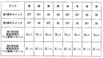
- FIG. 10 is a diagram showing a relationship between drive lines DL ′ 1 to DL ′ L for driving second signal lines and drive patterns corresponding to drive lines DL ′ L + 1 to DL ′ L + 6 in the second signal line driving period. Relationship between presence / absence of touch, ON / OFF signal of first operation switch and second operation switch, driving pattern of stylus pen in first signal line driving period, and driving pattern of stylus pen in second signal line driving period FIG.
- the touch panel system in Embodiment 2 of this invention is shown, Comprising: It is a block diagram which shows the structure of a touch panel system. A diagram showing the pen pressure value when there is a difference between the actual pen pressure value of the stylus pen, the pen pressure value updated / held inside the stylus pen, and the pen pressure value reproduced inside the touch panel controller. is there. It is a figure which shows the pen pressure value when the change part at the time of a continuous increase / decrease is provided in the unit increase / decrease amount change part of the conversion output part in a touch panel controller, and the increase / decrease amount per unit frequency is increased or decreased. It is a figure which shows an example of the adjustment method of the internal pen pressure value in a stylus pen.
- the touch panel system in Embodiment 3 of this invention is shown, Comprising: It is a block diagram which shows the structure of a touch panel system. It is a block diagram which shows the structure of the mobile telephone provided with the touchscreen system in Embodiment 4 of this invention.
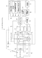
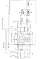
- FIG. 1 is a block diagram showing a configuration of a touch panel system 1 of the present embodiment
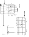
- FIG. 2 is a wiring diagram showing a configuration of a touch panel provided in the touch panel system.
- the touch panel system 1 of the present embodiment includes a touch panel 2, a stylus pen 3 as a touch pen and an electronic pen, and a touch panel controller 10 that drives the touch panel 2 and the stylus pen 3. .
- the touch panel 2 includes a plurality of K (K is a positive integer) first signal lines horizontal signal lines HL 1 to HL arranged in parallel with each other in the horizontal direction. and K, L present a plurality of which are arranged parallel to each other along the vertical direction (L is a positive integer) and a vertical signal line VL 1 ⁇ VL L as a second signal line. Capacitances C11 to CKL are generated at the intersections of the horizontal signal lines HL 1 to HL K and the vertical signal lines VL 1 to VL L , respectively. Note that K and L may be the same or different from each other, but in the present embodiment, description will be made assuming that L ⁇ K.
- the horizontal signal lines HL 1 to HL K and the vertical signal lines VL 1 to VL L intersect each other vertically.
- the present invention is not limited to this, and both are mutually connected. It is enough if they cross.
- the touch panel 2 is preferably wide enough to be worn by the hand holding the stylus pen 3, but may be a size used for a smartphone.
- the stylus pen 3 is not limited to a touch pen made of a conductor for making contact with the touch panel 2, but is a pen that can input and output a plurality of signals. As will be described later, the stylus pen 3 is provided with a synchronization signal detection circuit 35, and a synchronization signal for synchronizing with a dedicated synchronization signal generated by the timing generator 14 of the touch panel controller 10 is received and inputted. It has become so.
- the touch panel controller 10 includes a multiplexer 11, a driver 12, a sense amplifier 13, a timing generator 14, an AD converter 15, a capacity distribution calculation unit 16, a touch recognition unit 17, and a pen position detection unit 18. I have.
- the driver 12 applies the drive lines DL 1 to DL K or the drive lines DL 1 to DL L in response to the driving of the horizontal signal lines HL 1 to HL K or the vertical signal lines VL 1 to VL L described above on the touch panel 2.
- a voltage is applied.
- the stylus pen 3 outputs signals with drive waveforms corresponding to virtual drive lines DL L + 1 to DL L + 6 for the synchronization and writing pressure signal / first operation switch 38 and second operation switch 39. .
- the notations L + 1 to L + 6 are used to express L or K drive signal lines outside in the sense that the drive signal lines are not actually connected to the touch panel 2, and are actually connected to the touch panel.
- a waveform corresponding to an arbitrary drive signal line among unconnected drive signal lines may be used.
- the sense amplifier 13 generates signals of initial charges corresponding to the capacitances C11 to CKL of the touch panel 2 and a stylus pen at the time of touching when the horizontal signal lines HL 1 to HL K are driven in the first signal line driving period.
- the linear sum signal corresponding to the first pen charge signal which is the charge at the time of touch corresponding to the electrostatic capacity between 3 and the L vertical signal lines VL 1 to VL L is detected as the sense lines SL 1 to SL.
- the sense amplifier 13 generates signals of initial charges corresponding to the respective capacitances C11 to CKL of the touch panel 2 and a stylus at the time of touch when the vertical signal lines VL 1 to VL L are driven in the second signal line driving period.
- a linear sum signal corresponding to a second pen charge signal that is a charge at the time of touch corresponding to the capacitance between the pen 3 and each of the K horizontal signal lines HL 1 to HL K is expressed as a sense line SL 1 to It reads through SL K, and supplies to the AD converter 15.
- FIG. Figure 3 is a horizontal signal lines HL 1 - provided the touch panel 2 HL K, or vertical signal lines VL 1 ⁇ VL K ⁇ VL L and ⁇ driveline DL 1 which is connected to the driver DL K-DL L or sense 3 is a circuit diagram showing a configuration of a multiplexer that switches connection with sense lines SL 1 to SL K to SL L connected to an amplifier 13.
- FIG. 1 is a horizontal signal lines HL 1 - provided the touch panel 2 HL K, or vertical signal lines VL 1 ⁇ VL K ⁇ VL L and ⁇ driveline DL 1 which is connected to the driver DL K-DL L or sense 3 is a circuit diagram showing a configuration of a multiplexer that switches connection with sense lines SL 1 to SL K to SL L connected to an amplifier 13.
- FIG. 1 is a horizontal signal lines HL 1 - provided the touch panel 2 HL K, or vertical signal lines VL 1 ⁇ VL K ⁇ VL L and ⁇ driveline DL 1 which
- the multiplexer 11 is a connection switching circuit that switches connection between a plurality of inputs and a plurality of outputs.
- the horizontal signal lines HL 1 to HL K are connected to the drive lines DL 1 to DL K of the driver 12, and the vertical signal lines VL 1 to VL K to VL L are connected to sense amplifiers.
- 13 a first connection state of connecting to the sense line SL 1 ⁇ SL K ⁇ SL L of, connect the horizontal signal lines HL 1 ⁇ HL K to sense line SL 1 ⁇ SL K of the sense amplifier 13, the vertical signal line VL 1 ... VL K to VL L are switched to the second connection state in which the drive lines DL 1 to DL K to DL L of the driver 12 are connected.
- the horizontal signal lines HL 1 to HL K are connected to the drive lines DL 1 to DL K and the vertical signal lines VL 1 to VL L Are connected to the sense lines SL 1 to SL L.
- the horizontal signal lines HL 1 to HL K are connected to the sense lines SL 1 to SL K
- the vertical signal lines VL 1 to VL L are connected to the drive lines DL 1 to DL L. To be connected to.
- the timing generator 14 shown in FIG. 1 generates a signal that defines the operation of the driver 12, a signal that defines the operation of the sense amplifier 13, and a signal that defines the operation of the AD converter 15.
- the signals are supplied to the driver 12, the sense amplifier 13, and the AD converter 15, respectively.
- the timing generator 14 generates a synchronization signal.
- the touch panel controller 10 drives the horizontal signal lines HL 1 to HL K and the vertical signal lines VL 1 to VL L by using the synchronization signal generated by the timing generator 14 as a dedicated synchronization signal.
- the AD converter 15 includes charges corresponding to the capacitances C11 to CKL read through the vertical signal lines VL 1 to VL L and the sense lines SL 1 to SL L in the first signal line driving period, Capacitance distribution calculation by AD conversion of the linear sum signal corresponding to the first pen charge signal corresponding to the capacitance between the stylus pen 3 and each of the L vertical signal lines VL 1 to VL L To the unit 16.
- the AD converter 15 includes the charge corresponding to each of the capacitances C11 to CKL read through the horizontal signal lines HL 1 to HL K and the sense lines SL 1 to SL K in the second signal line driving period, and the stylus.
- Capacitance distribution calculation unit by AD converting a linear sum signal corresponding to the second pen charge signal which is a charge corresponding to the capacitance between the pen 3 and each of the K horizontal signal lines HL 1 to HL K 16 is supplied.
- the capacitance distribution calculation unit 16 calculates the capacitance distribution on the touch panel 2 based on the linear sum signal including the first pen charge signal and the second pen charge signal and the code sequence based on the drive, and The distribution of capacitance between the stylus pen 3 and each of the L vertical signal lines VL 1 to VL L and the static between the stylus pen 3 and each of the K horizontal signal lines HL 1 to HL K The distribution of capacitance is calculated, and the capacitance distribution on the touch panel 2 is supplied to the touch recognition unit 17, and the electrostatic capacitance between the stylus pen 3 and each of the L vertical signal lines VL 1 to VL L is calculated.
- the distribution of capacitance and the distribution of capacitance between the stylus pen 3 and each of the K horizontal signal lines HL 1 to HL K are supplied to the pen position detection unit 18 serving as position detection means.
- the touch recognition unit 17 recognizes the touched position on the touch panel 2 based on the capacitance distribution supplied from the capacitance distribution calculation unit 16.
- the pen position detection unit 18 determines the position along the horizontal signal line of the stylus pen 3 based on the distribution of capacitance between the stylus pen 3 and each of the L vertical signal lines VL 1 to VL L. To detect. Further, the pen position detection unit 18 determines the position along the vertical signal line of the stylus pen 3 based on the electrostatic capacitance distribution between the stylus pen 3 and each of the K horizontal signal lines HL 1 to HL K. Is detected.
- the horizontal signal lines HL 1 to HL K are connected to the drive lines DL 1 to DL K of the driver 12, and the vertical signal lines VL 1 to VL L are connected to the sense line SL of the sense amplifier 13.
- the driver 12 drives the horizontal signal lines HL 1 ⁇ HL K by applying a voltage to the drive line DL 1 ⁇ DL K.
- the charges accumulated in the respective capacitances C11 to CKL by driving the horizontal signal lines HL 1 to HL K and the stylus pen when the stylus pen 3 is brought close to the touch panel 2 are displayed.
- L first linear sum signals based on a first pen charge signal that is a charge corresponding to the capacitance between 3 and each of the L vertical signal lines VL 1 to VL L are L vertical signals. Output from each of the lines VL 1 to VL L.
- the sense amplifier 13 reads the L first linear sum signals including the first pen charge signal through the multiplexer 11 and the sense lines SL 1 to SL L, and supplies them to the AD converter 15.
- the AD converter 15 AD-converts the L first linear sum signals including the first pen charge signal and outputs the converted signals to the capacitance distribution calculation unit 16.
- the first connection state is switched to the second connection state so that the drive signals and sense signals of the horizontal signal lines HL 1 to HL K and the vertical signal lines VL 1 to VL L are interchanged. That is, in the second connection state, the horizontal signal lines HL 1 to HL K are connected to the sense lines SL 1 to SL K of the sense amplifier 13, and the vertical signal lines VL 1 to VL L are connected to the drive lines DL 1 to DL of the driver 12. Connect to L.
- the driver 12 drives the vertical signal lines VL 1 ⁇ VL L by applying a voltage to the drive line DL 1 ⁇ DL L.
- the charges accumulated in the electrostatic capacitors C11 to CKL by driving the vertical signal lines VL 1 to VL L , the stylus pen 3, and the K horizontal signal lines HL 1 to HL K second linear sum signals based on the second pen charge signal that is a charge corresponding to the capacitance between each of the K and K are output from each of the K horizontal signal lines HL 1 to HL K.
- the sense amplifier 13 reads the K second linear sum signals including the second pen charge signal through the multiplexer 11 and the sense lines SL 1 to SL K, and supplies them to the AD converter 15.
- the AD converter 15 AD-converts the K second linear sum signals including the second pen charge signal and outputs the converted signals to the capacitance distribution calculation unit 16.
- the capacitance distribution calculation unit 16 includes the first linear sum signal including the first pen charge signal, the second linear sum signal including the second pen charge signal, and the electrostatic on the touch panel 2.
- the capacitance distribution is calculated and supplied to the touch recognition unit 17, and the position along the horizontal signal line of the stylus pen 3 and the position along the vertical signal line of the stylus pen 3 are calculated and supplied to the pen position detection unit 18. To do.
- the touch recognition unit 17 recognizes the touched position on the touch panel 2 based on the capacitance distribution supplied from the capacitance distribution calculation unit 16.
- the pen position detection unit 18 is based on the position along the horizontal signal line of the stylus pen 3 calculated by the capacitance distribution calculation unit 16 and the position along the vertical signal line of the stylus pen 3. A position on the touch panel 2 is detected.
- the horizontal signal lines HL 1 to HL K and the vertical signal lines VL 1 to VL L are all driven simultaneously in parallel. That is, parallel driving is performed.
- the present invention is not limited to this, and the driving of the K horizontal signal lines HL 1 to HL K and the driving of the L vertical signal lines VL 1 to VL L on the touch panel 2 are either parallel driving or sequential driving. Also good.
- Parallel driving means driving K horizontal signal lines HL 1 to HL K or driving L vertical signal lines VL 1 to VL L simultaneously in parallel, and sequential driving means K horizontal signal lines.
- the driving of HL 1 to HL K or the L vertical signal lines VL 1 to VL L are sequentially driven from the horizontal signal line HL 1 or the vertical signal line VL 1 sequentially. From the viewpoint of speed, parallel driving is preferable, and in this embodiment, parallel driving is adopted.
- the touch panel system 1 includes the touch panel 2, the touch pen, and the touch panel controller 10 each having a capacitance formed at the intersections of the plurality of first signal lines and the plurality of second signal lines. I have.
- the touch panel controller 10 drives the horizontal signal lines HL 1 to HL K , which are a plurality of first signal lines, in the first signal line driving period, and outputs a charge signal based on each capacitance to a vertical signal that is each second signal line.
- the second signal line each first signal charge signals by driving the vertical signal lines VL 1 ⁇ VL L is a plurality of second signal lines in the driving period based on the electrostatic capacitance
- the touch pen is touched on the touch panel 2 to thereby change the charge accumulated in the capacitance of the touch pen. To detect the touch position.
- the detection position in the first signal line driving period is the same as the detection position in the second signal line driving period. Appears in position.
- an erroneous signal due to phantom noise caused by touching the touch panel 2 such as a human hand or finger that has received electromagnetic noise is caused by switching between the first signal line and the second signal line in the first signal line driving period. Appearing at the same position in the second signal line driving period.
- the touch position of the touch pen and an erroneous signal due to phantom noise are distinguished by determining the detection position based on the logical product of the detection position in the first signal line drive period and the detection position in the second signal line drive period. In addition, it is possible to remove an erroneous signal due to the phantom noise.
- Phantom noise is noise that generates a detection signal based on static electricity at a position different from the touch position of the touch pen through a hand holding the touch pen, and is different from the normal touch position of the touch pen. Is.
- the stylus pen 3 outputs a plurality of types of signals.
- the plural types of signals are, for example, signals related to a first operation switch 39a and a second operation switch 39b described later, and a signal related to the pen pressure sensor 31d. Note that these signals are merely examples, and the present invention is not necessarily limited thereto.
- FIG. 4 is a cross-sectional view showing the configuration of the stylus pen 3.
- the stylus pen 3 includes a pen body 30 that is held by a user and has a conductive grip portion 30 a formed in a substantially cylindrical shape so that the user can hold it by hand.
- the tip of the pen is provided with a pen tip 31 that is pressed against the touch panel 2 during a touch operation.
- the pen tip portion 31 is provided on the back side of the pen tip shaft 31b, a pen tip cover 31a, a pen tip shaft 31b, insulators 31c and 31c that hold the pen tip cover 31a in an axially movable manner, and the pen tip shaft 31b.
- a writing pressure sensor 31d is provided on the back side of the pen tip shaft 31b, a pen tip cover 31a, a pen tip shaft 31b, insulators 31c and 31c that hold the pen tip cover 31a in an axially movable manner, and the pen tip shaft 31b.
- the pen tip cover 31a is made of an insulating material, and the pen tip shaft 31b is made of a conductive material, for example, a metal or a conductive synthetic resin material.
- the writing pressure sensor 31d is composed of, for example, a semiconductor piezoresistive pressure sensor, and a semiconductor strain gauge is formed on the surface of a diaphragm (not shown). Therefore, when the pen tip cover 31a of the pen tip portion 31 is pressed against the touch panel 2 during the touch operation, the pen tip shaft 31b is pushed through the pen tip cover 31a to press the surface of the diaphragm of the writing pressure sensor 31d, Thereby, a change in electric resistance due to the piezoresistance effect generated by the deformation of the diaphragm is converted into an electric signal. Thereby, the writing pressure in the stylus pen 3 can be detected. Note that the principle of pen pressure detection is not necessarily limited to this, and other detection principles can be employed.
- connection switch 32 In the pen body 30, a connection switch 32, a control circuit 33, operation changeover switches 34a and 34b, a sense circuit 35, a synchronization signal detection circuit 36, a timing adjustment circuit 37, and a drive circuit 38 are provided. Is provided.
- the connection switch 32 can be omitted. When the connection switch 32 is omitted, the output of the control circuit 33 is connected to the pen tip shaft 31b.
- connection switch 32 is an electronic switch composed of a field effect transistor (FET) or the like, and is turned on / off by the control circuit 33.
- FET field effect transistor
- the connection switch 32 is off, the pen tip cover 31 a is electrically disconnected from the grip portion 30 a of the pen body 30.
- the touch panel system 1 does not recognize the proximity / contact of the stylus pen 3 even if the pen tip cover 31 a is brought close to the touch panel 2.
- the connection switch 32 when the connection switch 32 is turned on, the pen tip cover 31a is electrically connected to the grip portion 30a of the pen body 30 via the pen tip shaft 31b, and the human body is connected to the pen tip cover 31a via the grip portion 30a.
- Conduct since the human body has a relatively large capacitance, when the stylus pen 3 approaches or comes into contact with the touch panel 2, the charges accumulated in the capacitances C11 to CKL of the touch panel 2 change, and the touch panel 2 changes.
- the system 1 can detect the touch state of the stylus pen 3.
- the stylus pen 3 is provided with, for example, a push-type first operation switch 39a and a second operation switch 39b.
- a push-type first operation switch 39a and a second operation switch 39b By pressing the first operation switch 39a and the second operation switch 39b, the first operation switch 39a and the second operation switch 39b are pressed.
- the functions assigned to the first operation switch 39 a and the second operation switch 39 b are executed via the control circuit 33.
- An example of the function assigned to the first operation switch 39a is an eraser function.
- the eraser function can be turned on / off by the first operation switch 39a.
- a function assigned to the second operation switch 39b for example, a right click function of the mouse can be cited, and the right click function of the mouse can be turned on / off by the second operation switch 39b. is there.
- eraser function and the right-click function of the mouse are examples, and are not limited to the eraser function and the right-click function of the mouse. It is also possible to add other functions by providing other operation switches.
- the touch signal to the touch panel 2 of the stylus pen 3 that is, the first pen charge signal and the second pen charge signal described above, touch the stylus pen 3 on the touch panel 2 with the connection switch 32 of the stylus pen 3 turned on.
- the touch position is detected by switching driving between the horizontal signal lines HL 1 to HL K and the vertical signal lines VL 1 to VL L.
- the drive pattern of the stylus pen 3 is driven by the drive circuit 38 in the first signal line drive period.
- the drive pattern of the horizontal signal lines HL K + 1 and HL K + 2 (or later) of the touch panel 2 by the touch panel controller 10 that is, the K + 1 and K + 2 (or later) drive lines DL K + 1 and DL K + 2 (or later) of the driver 12.
- Th (or later) dora Adopts a method of matching the driving pattern of brine DL L + 1 ⁇ DL L + 2 ( or later).
- the horizontal signal lines HL K + 1 ⁇ HL K + 2 (or later) and the vertical signal lines VL L + 1 ⁇ VL L + 2 (or later) themselves do not exist.
- the drive pattern may be different depending on the drive period (K ⁇ L) as in the drive line DL K + 1 or the drive line DL L + 1.
- a virtual line is displayed using the notation of the line DL L + 1 . In the following description, it will be expressed as drive line DL L + 1 .
- the touch panel controller 10 made by waveform corresponding to the drive line DL L + 1 ⁇ DL L + 2, the increase and decrease signals writing pressure sensor 31d of the stylus 3, and that can be retrieved via the sense line SL 1 ⁇ SL L ing. That is, in the present embodiment, an increase / decrease signal of the writing pressure sensor 31d in the stylus pen 3 is output by a waveform corresponding to the drive lines DL L + 1 and DL L + 2 , and passes through the position of the touch panel 2 touched at that time. Detection is performed on the sense lines SL 1 to SL L via the horizontal signal lines HL 1 to HL K or the vertical signal lines VL 1 to VL L.
- the stylus pen 3 of the present embodiment transmits and receives signals to and from the touch panel controller 10 wirelessly. Therefore, the pen tip 31 is driven in the same pattern as driving the drive lines DL L + 1 to DL L + 6 so as to match the drive timing of the drive lines DL 1 to DL L in the touch panel controller 10.
- the stylus pen 3 is provided with a drive circuit 38 to drive in the same manner as the driver 12 of the touch panel controller 10.
- the drive of the drive lines DL 1 to DL L in the touch panel controller 10 is based on the drive timing generated by the timing generator 14. For this reason, the stylus pen 3 must also be operated in synchronization with the timing when the touch panel controller 10 is driven. Therefore, in the stylus pen 3 of the present embodiment, by providing the sense circuit 35, the synchronization signal detection circuit 36, and the timing adjustment circuit 37, the timing of the dedicated synchronization signal driven by the touch panel controller 10 with the stylus pen 3 and the stylus pen 3, the timing of the pen synchronization signal generated by the timing adjustment circuit 37 is matched.
- FIG. 5 is a timing chart showing the basic principle of how to synchronize.
- the stylus pen 3 detects the dedicated synchronization signal generated by the timing generator 14 of the touch panel controller 10 by the sense circuit 35 and the synchronization signal detection circuit 36.
- the dedicated synchronization signal is a single pulse.
- the touch panel synchronization signal S0 which is a dedicated synchronization signal composed of a single pulse, is generated at a constant cycle.
- the sense circuit 35 generates a plurality of synchronization signal candidates S1 to Sp (p is an integer of 2 or more).
- the synchronization signal candidate Sp shown in FIG. 5 represents a signal in which the synchronization signal candidate S1 is delayed by about one cycle.
- the stylus pen 3 selects a synchronization signal having a high degree of coincidence with the dedicated synchronization signal transmitted from the timing generator 14 of the touch panel controller 10 from among the synchronization signal candidates S1 to Sp, and serves as a synchronization signal for communication with the touch panel controller 10. adopt.
- the synchronization signal candidate S4 or S5 having a high degree of coincidence with the touch panel synchronization signal S0 is employed as the pen synchronization signal of the stylus pen 3.
- the stylus pen 3 is in a detection mode until the synchronization is established, and the drive circuit 38 is not driven.
- the stylus pen 3 can be synchronized with the dedicated synchronization signal in the touch panel controller 10.
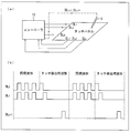
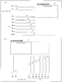
- FIG. 6A is a diagram illustrating an output relationship to the touch panel and the stylus pen in the driver drive line and the sense amplifier sense line in the touch panel controller
- FIG. 6B illustrates a synchronization waveform and a touch detection waveform. It is a waveform diagram.
- FIG. 7A is a waveform diagram showing a drive waveform such as a synchronization waveform and a touch detection waveform transmitted from the touch panel controller to the stylus pen, and low frequency noise
- FIG. 7B is a waveform showing the drive waveform and low frequency noise.
- FIG. 7A is a waveform diagram showing a drive waveform such as a synchronization waveform and a touch detection waveform transmitted from the touch panel controller to the stylus pen, and low frequency noise
- FIG. 7B is a waveform showing the drive waveform and low frequency noise.
- FIG. 7A is a waveform diagram showing a drive waveform such as a synchronization waveform and a touch detection waveform transmitted from the touch panel controller to the styl
- FIG. 7C is a waveform diagram showing a state where reset is performed at the reset timing.
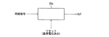
- FIG. 8 is a diagram showing a configuration of a reset circuit provided in the synchronization signal detection circuit in the stylus pen.
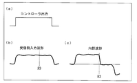
- FIG. 9A is a waveform diagram illustrating an example of a synchronization waveform transmitted from the touch panel controller
- FIG. 9B is a waveform diagram illustrating an input waveform at the stylus pen that is a reception
- FIG. FIG. 9B is a waveform diagram showing an internal waveform when a reference potential is determined at reset timing R1 in FIG. 9B
- FIG. 9D is a reference potential determined at reset timing R2 in FIG. 9B.
- It is a wave form diagram which shows an internal waveform at the time.
- FIG. 9A is a waveform diagram illustrating an example of a synchronization waveform transmitted from the touch panel controller
- FIG. 9B is a waveform diagram illustrating an input waveform at the stylus pen that is a reception
- FIG. 10A is a waveform diagram showing a synchronization waveform using the M-sequence code “1110010” when Manchester encoding is not performed
- FIG. 10B is a synchronization diagram using the Manchester-encoded M-sequence code “1110010”.
- It is a wave form diagram which shows a waveform.
- FIG. 11A is a waveform diagram showing an example of a synchronization waveform having a long High period transmitted from the touch panel controller
- FIG. 11B is a waveform diagram showing reset timing R3 of the input waveform at the stylus pen that is reception.
- FIG. 11C is a waveform diagram showing an internal waveform when the reference potential is determined at the reset timing R3 in FIG. 11B.
- FIG. 11A is a waveform diagram showing a synchronization waveform using the M-sequence code “1110010” when Manchester encoding is not performed
- FIG. 10B is a synchronization diagram using the Manchester-encoded M-s
- FIG. 12A is a diagram showing a synchronous waveform of a pseudo-randomized sequence having Manchester-coded periodicity transmitted from a touch panel controller to a stylus pen in the touch panel system, and FIG. It is a wave form diagram which shows the waveform for touch detection.
- the dedicated synchronization signal of the touch panel controller 10 is generated by the timing generator 14 of the touch panel controller 10 and is driven by the driver 12 to the drive lines DL 1 to DL. Transmitted using L. Then, as a mechanism for notifying the stylus pen 3 of a dedicated synchronization signal that is the driving timing of the touch panel controller 10, as shown in FIG. 6B, driving with a waveform representing synchronization separately from a normal touch detection waveform.
- the lines DL 1 to DL L are driven. Specifically, in each of the drive lines DL 1 to DL L , a waveform for touch detection is generated after a synchronization waveform is generated.
- the waveform for touch detection is generated by sequential driving.
- the generation of the synchronous waveform is indicated by a plurality of continuous pulses in order to facilitate visual distinction from the sequential drive waveform, and is actually proposed in this embodiment.
- the waveform obtained by Manchester encoding the existing M-sequence code or the like is easier to detect as a synchronous waveform.
- the signal waveform received by the stylus pen 3 is mixed with various types of noise, particularly low frequency noise.
- FIG. 7A it is assumed that a dedicated synchronization waveform composed of a plurality of dense pulses driven by the touch panel controller 10 and indicated by a sin curve is noise.
- the signal waveform received by the stylus pen 3 is obtained by superimposing the synchronization waveform from the touch panel controller 10 and low-frequency noise, as shown in FIG. 7B.
- the signal waveform received by the stylus pen 3 has a larger amplitude of low-frequency noise than the amplitude of the synchronous waveform from the touch panel controller 10 to be extracted.
- the amplitude of the synchronous waveform signal is a signal having a relatively small amplitude compared to the noise, making it difficult to extract the synchronous waveform signal. .
- a method of finding the synchronization waveform from the waveform in which the synchronization waveform and the low frequency noise shown in FIG. 7B are superimposed for example, a method of removing low frequency noise with a low frequency cut filter, a synchronization waveform.
- the low frequency cut filter is expensive.
- the stylus pen 3 on the reception side of the synchronization waveform performs a reset operation for determining a reference potential for the received input waveform, and the amplitude of the internal waveform is increased by the potential difference from the reference potential.
- the present invention is not necessarily limited to this, and it is also possible to remove noise composed of low frequency components using a low frequency cut filter.
- the synchronization signal detection circuit 36 of the stylus pen 3 includes a reset circuit 36a shown in FIG. 8 in order to perform a reset operation for determining a reference potential for the received input waveform.
- a reset is performed on the superimposed signal waveform in which the synchronization waveform from the touch panel controller 10 illustrated in FIG. 7B and the low-frequency noise are superimposed.
- the superimposed signal waveform is returned to the reference potential at the reset timing. That is, the reference potential is set to the same potential as the input signal. If the potential of the input superimposed signal waveform is higher than the reference potential, a positive potential is output. On the other hand, if the potential of the input superimposed signal waveform is lower than the reference potential, a negative potential is output. As a result, it is possible to remove low frequency components and keep the amplitude of the signal within a certain range.
- the reference potential of the stylus pen 3 on the receiving side is determined when performing a reset operation for determining the reference potential for the received input waveform.
- the reset timing and the pulse of the synchronization waveform overlap, there is a problem that the pulse is missed and it becomes difficult to determine the dedicated synchronization signal that is the drive timing of the touch panel controller 10.
- the input waveform in the stylus pen 3 on the receiving side is shown by the waveform in FIG. 9B.
- the internal waveform when the reference potential is determined at the reset timing R1 is shown in FIG. 9C.
- the reset timing R2 is set to the second pulse in the waveform of FIG. 9B
- the internal waveform when the reference potential is determined is as shown in FIG. 9D.
- the second pulse since the second pulse has no positive rise, the second pulse is missed. That is, it becomes difficult to determine the dedicated synchronization signal that is the drive timing of the touch panel controller 10.
- a constant pattern synchronization signal composed of a pseudo-randomized sequence having periodicity is used as the synchronization waveform transmitted by the touch panel controller 10.
- an M-sequence code or a Gold sequence code is used.
- the pseudo-randomized sequence is a code sequence used for a pseudorandom signal which is an artificially generated random signal. That is, a truly irregular signal that exists in nature is usually called a random signal (random signal), whereas an artificially generated random signal is converted to a pseudorandom signal (pseudorandom signal). ). Since it is created artificially, a certain rule is necessary, but various measures have been taken so that the statistical properties of the generated signal are as close as possible to those of a true irregular signal. Usually, the autocorrelation function of the generated signal is devised so as to be as close as possible to the autocorrelation function ⁇ (t) of white noise.
- the pseudo irregular signal is generated by associating a pseudo irregular series (numerical string) with a physical quantity such as a voltage.
- the pseudorandom sequence includes a finite-length sequence and a periodic sequence, and a periodic sequence is often used from the viewpoint of ease of generation and ease of use.
- Typical examples of the periodic sequence include an M sequence (M-sequence) and a gold sequence.
- the autocorrelation of the M-sequence signal and the Gold sequence code has a very sharp peak, and the correlation value with others is very low.
- the M series and the Gold series are composed of binary numbers of 0 and 1, and have a periodicity in which binary series are connected.
- this M-sequence code or Gold sequence code as a synchronization waveform transmitted by the touch panel controller 10, even if the reset timing overlaps with one pulse, the code that matches this M-sequence code is correct. Since it is only necessary to determine the synchronization timing, the reliability of the synchronization determination is increased.
- an M-sequence code is used as a synchronization waveform to be transmitted by the touch panel controller 10, and the synchronization signal detection circuit 35 of the stylus pen 3 determines coincidence with the same M-sequence code, thereby missing a pulse.
- the synchronization waveform transmitted by the touch panel controller 10 includes a pulse that is high for a long period as shown in FIG. 11A, and the received input waveform of the stylus pen 3 shown in FIG.
- the internal waveform when the reference potential is determined at the timing R3 is as shown in FIG. 11C, which makes detection difficult.
- the touch panel controller 10 is driven as a synchronous waveform using a Manchester encoded waveform for a code having good autocorrelation characteristics such as an M-sequence.
- the Manchester-encoded waveform means that “0” corresponds to High ⁇ Low of the synchronization waveform and “1” corresponds to Low ⁇ High of the synchronization waveform. Say. Note that this may be reversed.
- the M-sequence code “1110010” when used, it is possible to prevent a case where the High or Low period is long.
- FIG. 12 (a) for example, the above-described 7-bit M-sequence code “1110010”, which is Manchester-encoded, is used as shown in FIG. 12 (a).
- FIG.12 (b) it uses as a synchronous waveform of the touch panel controller 10.
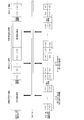
- FIG. 13 is an operation image diagram showing a correspondence relationship between the driving operation of the touch panel controller 10 and the driving operation of the stylus pen 3.
- FIGS. 14A, 14B, and 14C are diagrams showing specific drive operations in the synchronization signal detection period, the pause period, and the normal drive period shown in FIG.
- the driving operation of the stylus pen 3 is performed by turning on the operation changeover switch 34 a and turning off the operation changeover switch 34 b to generate a synchronization signal from the touch panel controller 10 by the sense circuit 35 and the synchronization signal detection circuit 36.
- the synchronization signal detection period is a waiting period for detecting a bit pattern representing a synchronization waveform, and is a period for detecting the synchronization signal pattern from the pen tip signal waveform by turning off the pen tip 31 drive. Specifically, in the synchronization signal detection period, as shown in FIG. 14A, the drive lines DL 1 to DL L of the driver 12 are driven with the same waveform. A waveform pattern including a pattern having an autocorrelation characteristic such as an M series is used.
- a code to be driven is selected based on the additional information after detection of the synchronization signal pattern and the state of the stylus pen 3 itself, and preparation for starting to drive the pen tip in synchronization with the touch panel controller 10 is performed. This is a period for interpreting additional information that takes the drive start timing.
- the drive mode period is a period in which the pen tip unit 31 is driven by the drive circuit 38, and the pen tip unit 31 is selected with the selected code while finely adjusting the edge of the drive waveform so as to match the drive timing of the touch panel controller 10. This is a period for driving. At this time, the drive circuit 38 of the stylus pen 3 is driven in accordance with the drive timing of the touch panel controller 10.
- the driving operation of the touch panel controller 10 switches the drive lines DL 1 to DL L with the same waveform, the idle period, and the drive lines DL 1 to DL K and the sense lines SL1 to SL K to SL L. It is configured by repeating three periods with a driving period.
- the period during which the drive lines DL 1 to DL L are driven with the same waveform is a period for driving the synchronization waveform plus additional information for the stylus pen 3 to synchronize. Specifically, as shown in FIG. 14B, the drive lines DL 1 to DL L are driven with the same waveform.
- the pause period is a period in which the stylus pen 3 finishes synchronization detection and a period for preparing for driving. Specifically, as shown in FIG. 14B, it is a waiting time for providing a preparation period in which the stylus pen 3 detects a synchronous waveform and performs normal driving. For this reason, the driving waveform has no meaning and is completely arbitrary. Therefore, it is not necessary to drive. Note that this section is not necessary when the preparation period on the stylus pen 3 side is unnecessary.
- the normal driving period for a period the position detection for obtaining an worth of data of the touch panel 2 for driving switching between ⁇ driveline DL 1 ⁇ DL K ⁇ DL L and the sense lines SL1 SL K-SL L It is.
- this normal drive period as shown in FIG. 14C, the drive lines DL 1 to DL K to DL L are repeatedly driven and sensed with a waveform necessary for detecting the touch position of the stylus pen 3. .
- sequential driving or parallel driving is performed.
- the order of drive patterns is expressed by sequential drive so that it can be easily understood visually.
- the stylus pen 3 drives the pen tip 31 with the same waveform as that of the drive lines DL L + 1 and DL L + 2 corresponding to the outside of the touch panel 2 when the synchronization waveform can be detected.
- the background is colored in the sense period, that is, the period in which the signal based on the charge accumulated in the capacitance for detecting the touch position is detected.
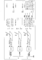
- FIG. 15 is a diagram illustrating a relationship between a driver drive pattern in the touch panel controller and a drive circuit drive pattern in the stylus pen.
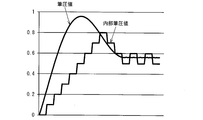
- FIG. 16 is a diagram illustrating a pen pressure value obtained with the stylus pen and a pen pressure value expressed in the stylus pen and the touch panel controller of the pen pressure.
- the stylus pen 3 includes the writing pressure sensor 31d, and includes an electronic pen that outputs a quantitative characteristic value such as a writing pressure level. For this reason, in order to send the quantitative characteristic value detected by the stylus pen 3 to the touch panel controller 10 side, since there are many information types, it cannot be sent without using various identification signals. As a result, there are problems that the amount of signal increases, transmission takes time, and identification of the signal on the receiving side is complicated.
- the stylus pen 3 includes an electronic pen that outputs a quantitative characteristic value, and the stylus pen 3 is an L + 1th drive signal line. It is output that the quantitative characteristic value in the stylus pen 3 has increased from the characteristic value at the previous output in a waveform corresponding to the drive line DL L + 1 . On the other hand, the quantitative characteristic value in the stylus pen 3 has decreased from the characteristic value updated and held at the previous output in the waveform corresponding to the drive line DL L + 2 as the L + 2th drive signal line. Is output. Further, in order to determine the next increase / decrease, the output result of the current increase / decrease is reflected in the characteristic value held internally.
- the touch panel controller 10 outputs the initial value of the quantitative characteristic value and the number of outputs per unit number of times in the waveform corresponding to the ( L + 1) th drive line DL L + 1 or the waveform corresponding to the (L + 2) th drive line DL L + 2.
- a conversion output unit 19 that converts and outputs a quantitative characteristic value based on the sum of the quantity is provided.
- the stylus pen 3 when the stylus pen 3 detects the writing pressure with the writing pressure sensor 31d, the writing pressure value of the writing pressure sensor 31d increases from the value when it was last output.
- the driver 12 of the touch panel controller 10 drives the drive lines DL 1 to DL L , the stylus pen 3 drives the pen tip 31 with a waveform corresponding to the drive line DL L + 1 .
- the stylus pen 3 detects the writing pressure with the writing pressure sensor 31d, if the writing pressure value of the writing pressure sensor 31d is smaller than the value when it was last output, the driver of the touch panel controller 10 When 12 drives the drive lines DL 1 to DL L , the stylus pen 3 drives the pen tip 31 with a waveform corresponding to the drive lines DL L + 2 .
- an increase / decrease signal of the writing pressure sensor 31d in the stylus pen 3 is output by a waveform corresponding to the drive lines DL L + 1 and DL L + 2 , and the horizontal signal line HL 1 passing through the position of the touch panel 2 touched at that time is output. Detected by the sense lines SL 1 to SL L through HL K or the vertical signal lines VL 1 to VL L.
- the value when it was output last time that is, the characteristic value held internally
- the value at the previous transmission that is, the characteristic value held internally is “0”.
- the interval at which the writing pressure increase / decrease signal of the writing pressure sensor 31d is sent from the stylus pen 3 is once in the driving period in which the driver 12 drives the drive lines DL 1 to DL L once.
- driving by sequential driving is shown for easy understanding, but driving by parallel driving may be used.
- the stylus pen 3 transmits only two types of information indicating whether the quantitative characteristic value has increased or decreased from the characteristic value at the previous output.
- the touch panel controller 10 side can grasp whether the writing pressure value of the writing pressure sensor 31d has increased or decreased.
- the touch panel controller 10 is provided with a conversion output unit 19, and the summation unit 19a of the conversion output unit 19 uses the initial value of the quantitative characteristic value and the (L + 1) th drive.
- Quantitative characteristic values are converted and output based on the sum of the number of times of output corresponding to the waveform corresponding to the line DL L + 1 or the waveform corresponding to the (L + 2) th drive line DL L + 2 ⁇ the increase / decrease amount per unit number. .
- the signal processing in the conversion output unit 19 of the touch panel controller 10 on the receiving side is simple because only the cumulative value of increase / decrease with respect to the initial value of the quantitative characteristic value is obtained.
- the pen pressure value shown in FIG. 16 can be obtained.
- the initial value starts from “0”.
- the pen pressure value takes a value in the range of 0 to 1.0
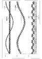
- the pen pressure value obtained at the pen tip portion 31 of the actual stylus pen 3 is shown by a curve in FIG. .
- the stylus pen 3 represents the writing pressure as a value in increments of 0.2 as an internal process.
- This internal processing is performed by the control circuit 33 of the stylus pen 3.
- the control circuit 33 it is determined whether the internal pen pressure value is increased or decreased, the pen pressure value of the curve is approached, and based on this determination, the internal pen pressure value is updated and increased or decreased. Is represented as a driving waveform of the pen tip 31.
- the conversion output unit 19 uses the initial value “0” as a reference and the sum of the number of outputs ⁇ the increase / decrease amount per unit number “0.2”. It is possible to reproduce the same pen pressure value change as the internal pen pressure value.
- the touch panel system 1 that can easily output the information in a short time can be provided.
- the two types of increase / decrease signals that output quantitative characteristic values such as the pen pressure level are as described above.
- the on / off signal of the first operation switch 39a and the on / off signal of the second operation switch 39b are output to the stylus pen 3, the on / off of the first operation switch 39a is output.
- a drive pattern indicating an on / off signal of the second operation switch 39b is performed by performing output by a drive pattern indicating a signal every time or once in a plurality of times in either the first signal line drive period or the second signal line drive period.
- a control circuit 33 is provided as a control unit that performs the output according to the above from the other of the second signal line driving period and the second signal line driving period each time or once every plural times.
- the first operation switch At least one of the on / off signal 39a and the on / off signal of the second operation switch 39b is output only once in a plurality of times in the first signal line driving period or the second signal line driving period. That is, the data is thinned and output only once in a plurality of times in the first signal line driving period or the second signal line driving period.
- the touch panel system 1 which can shorten the driving time in the sequential driving, reduce the driving / decoding range in the parallel driving, and easily increase the touch pen. Can do.
- the four driving patterns are required only by the on / off signals of the first operation switch 39a and the second operation switch 39b, but the four driving patterns are maintained to indicate the presence or absence of touch.
- the information indicating the presence / absence of the touch here has a certain threshold value in the control circuit 33 such that, for example, the touch pressure sensor 31d detects that even a slight writing pressure is detected, and if not, there is no touch. It shall be judged.
- an on / off signal of the first operation switch 39 a and a signal indicating the presence or absence of a touch are sent each time.
- the sense amplifier 13 detects a state in which the pen tip portion 31 is driven with a driving pattern corresponding to the drive lines DL L + 3 to DL L + 6 , while touching an on / off signal of the second operation switch 39b.
- the sense amplifier 13 detects a state in which the pen tip portion 31 is driven with a drive pattern corresponding to the drive lines DL ′ L + 3 to DL ′ L + 6 in each second signal line drive period. Can do.
- the pen tip has a drive pattern corresponding to the drive line DL ′ L + 3 in each second signal line drive period.
- the pen point unit 31 is driven with a driving pattern corresponding to the drive line DL ′ L + 4 in each second signal line driving period.
- the pen tip is driven with a driving pattern corresponding to the drive line DL ′ L + 5 in each first signal line driving period.
- the pen point unit 31 is driven with a drive pattern corresponding to the drive line DL ′ L + 6 in each second signal line drive period.
- the drive patterns corresponding to the drive lines DL L + 3 to DL L + 6 for the first signal line drive period and the drive lines DL ′ L + 3 to DL ′ L + 6 for the second signal line drive period are used.
- the drive patterns are distinguished from each other, they may be substantially the same.
- the first signal line drive period and the second signal line drive are respectively set to the on / off state of the first operation switch 39a and the on / off states of the second operation switch 39b. Instead of outputting every time with a period, it is output alternately. As a result, in addition to the presence or absence of touch, each of the on / off states of the first operation switch 39a and the second operation switch 39b is output to both the first signal line drive period and the second signal line drive period.
- Drive patterns corresponding to the eight drive lines DL L + 3 to DL L + 10 are required, but when output alternately, the drive patterns correspond to the four drive lines DL L + 3 to DL L + 6 . A drive pattern is sufficient.
- the stylus pen 3 when the stylus pen 3 outputs the on / off state of the first operation switch 39a and the on / off state of the second operation switch 39b,
- the first operation switch 39a outputs the drive pattern indicating the on / off state every time or a plurality of times in either the first signal line drive period or the second signal line drive period.
- a control circuit 33 as a control unit for performing output by a drive pattern indicating the on / off state of 39b from the second signal line drive period or the second signal line drive period every time or once every plural times. Yes.
- the first signal line drive When each cycle of the first signal line drive period or the second signal line drive period is sufficiently short and can be used practically without feeling uncomfortable even if it does not represent each state, the first signal line drive The data is thinned and output only once in a plurality of periods or the second signal line driving period.
- the touch panel system 1 in which the driving time is shortened in the sequential driving, the driving / decoding range is reduced in the parallel driving, and the number of touch pens is easily increased.
- an output based on a drive pattern indicating the on / off state of the first operation switch 39a is performed in each first signal line drive period, while the second operation switch 39b is turned on. Output with a drive pattern indicating an off state is performed every second signal line drive period.
- the on / off state of the first operation switch 39a and the on / off state of the second operation switch 39b are output each time both in the first signal line driving period and the second signal line driving period. Instead of using it, you can also use it for alternate output.
- the number of drive patterns that is half of the original number is sufficient, so that a touch panel system that can output the signals in a short time can be provided.
- the control circuit 33 outputs the drive pattern indicating the on / off state of the first operation switch 39a of the stylus pen 3 and the on / off state of the second operation switch 39b. Is driven by a drive pattern corresponding to the L + 1 and subsequent drive lines DL L + 1 to DL L + 6 different from the L drive lines DL 1 to DL L of the driver 12 (L is a positive integer equal to or greater than 2).
- the stylus pen 3 has the on / off signal of the first operation switch 39a and the on / off of the second operation switch 39b as the first pen function signal and the second pen function signal.
- the signal can be detected by bringing the stylus pen 3 into contact with the touch panel 2 or approaching the electrostatic detection range.
- the first operation switch 39 a is turned on / off via the plurality of first signal lines or the plurality of second signal lines arranged on the touch panel 2.
- the on / off state of the second operation switch 39b can be detected. That is, when the pen tip portion 31 of the stylus pen 3 is approaching the touch panel 2 but is not touched, the pen tip portion 31 is driven with a drive pattern indicating a state of not touching. The state of not touching can be read through the touch panel 2.
- the driver 12 serving as the synchronization signal transmission unit of the touch panel controller 10 includes the horizontal signal lines HL 1 to HL K as the plurality of first signal lines or the plurality of second signal lines. It also serves as a driver 12 as a drive unit for supplying a drive signal for driving the vertical signal lines VL 1 to VL L of the plurality of horizontal signal lines HL 1 to HL K or a plurality of vertical signal lines VL 1 to VL L.
- the drive signal for driving the signal lines VL 1 to VL L is changed to a waveform formed of a Manchester-encoded pseudo-random sequence having periodicity, and a synchronization signal is transmitted.
- the synchronization signal transmission unit is composed of the driver 12 that also serves as the drive unit, and therefore the drive lines DL 1 to DL for driving the horizontal signal lines HL 1 to HL K and the vertical signal lines VL 1 to VL L.
- a synchronization signal can be created simply by changing the waveform pattern of the L drive signal. For this reason, since a separate circuit for generating the synchronization signal is not provided, the number of parts can be reliably reduced. As described above, this effect is limited to the case where the synchronization signal uses the M series in the case of parallel driving.
- the stylus pen 3 as a touch pen and horizontal signal lines HL 1 to HL K and L (K) (K is an integer of 2 or more) first signal lines.
- L is an integer satisfying L ⁇ K)
- the touch panel controller 10 uses the drive signals for driving the K horizontal signal lines HL 1 to HL K or the L vertical signal lines VL 1 to VL L as L drive signal lines from a driver 12 as a drive unit.
- a sense amplifier 13 serving as a detection unit is output via the drive lines DL 1 to DL L and the touch panel 2 is touched with the stylus pen 3 to change the electric charge accumulated in the capacitance of the stylus pen 3.
- the detection signals from the K horizontal signal lines HL 1 to HL K or the L vertical signal lines VL 1 to VL L are input via the sense lines SL 1 to SL L as L detection signal lines. To do.
- the stylus pen 3 includes an electronic pen that outputs a quantitative characteristic value.
- the stylus pen 3 has a quantitative characteristic in the stylus pen 3 in a waveform corresponding to the ( L + 1) th drive line DL L + 1. While the output value is larger than the characteristic value at the previous output, the quantitative characteristic value at the stylus pen 3 is the characteristic value at the previous output in the waveform corresponding to the ( L + 2) th drive line DL L + 2. Output that it has decreased.
- the touch panel controller 10 also outputs the initial value of the quantitative characteristic value and the number of outputs per unit number of times of the waveform corresponding to the ( L + 1) th drive line DL L + 1 or the waveform corresponding to the (L + 2) th drive line DL L + 2.
- a conversion output unit 19 that converts and outputs a quantitative characteristic value based on the sum of the increase / decrease amount is provided.
- the signal processing on the receiving side is simple because it only requires the cumulative value of the increase / decrease relative to the initial value of the quantitative characteristic value.
- the touch panel system 1 that can easily transmit the information in a short time can be provided.
- the stylus pen 3 as an electronic pen includes, for example, a pen pressure sensor 31d.
- a pen pressure sensor 31d thereby, when the stylus pen 3 is touched on the touch panel 2, it is possible to detect a writing pressure level which is a quantitative characteristic value.
- the touch panel system 1 according to the present embodiment is different in that the conversion output unit 19 of the touch panel controller 10 can change the amount of increase / decrease per unit number of times.
- FIG. 19 is a block diagram showing a configuration of the touch panel system 1 of the present embodiment.
- the conversion output unit 19 is provided with a unit increase / decrease amount change unit 19b that changes the increase / decrease amount per unit number of times.
- a unit increase / decrease amount change unit 19b is provided in the conversion output unit 19, and the unit increase / decrease amount change unit 19b changes the increase / decrease amount per unit number of times. Therefore, it can suppress that a difference arises between the actual quantitative characteristic values in the stylus pen 3.
- the conversion output unit 19 can detect only how many times the output corresponding to the waveform corresponding to the (L + 1) th drive signal line or the waveform corresponding to the (L + 2) th drive signal line has been output in a certain time. Therefore, it is a problem how to determine whether or not the unit increase / decrease amount change unit 19b changes the increase / decrease amount per unit number of times.
- the unit increase / decrease amount change unit 19b is provided with a continuous increase / decrease change unit 19c, and the continuous increase / decrease change unit 19c corresponds to the (L + 1) th drive signal line.
- P is an integer of 2 or more
- the change speed is sufficient even for the same pen pressure change. Sometimes you can't keep up.
- the increase / decrease amount per unit number is increased from 0.1 to 0.2. If the pen pressure value continues to increase or decrease once more, the increase / decrease amount per unit number is further increased to 0.3.
- the increase / decrease amount per unit number is decreased. Further, if the increase or decrease is continuously repeated, the increase / decrease amount per unit number is further reduced. Thus, for example, if the increase or decrease continues twice, the increase / decrease amount per unit number of times is increased, and if not, the increase / decrease amount per unit number of times is decreased.
- the amount of increase / decrease per unit number is increased / decreased in increments of 0.1.
- the increase / decrease width of the increase / decrease amount per unit number is 0.1 or more and 0.3 or less.
- the unit increase / decrease amount change unit 19b is provided in the touch panel controller 10 to reproduce the writing pressure value.
- the unit increase / decrease amount change unit 19b and the continuous increase / decrease change unit are provided on the stylus pen 3 side.
- 19c may be provided and transmitted to the touch panel controller 10 side.
- the conversion output unit 19 of the touch panel controller 10 determines the amount of increase / decrease per unit number of times within the stylus pen 3 depending on how many times the increase or decrease of the pen pressure value continues as long as the increase or decrease of the pen pressure value is known.
- the same writing pressure as the internal writing pressure value of the stylus pen 3 can be reproduced by this changing width and increase / decrease information.
- the internal writing pressure value of the stylus pen 3 is output, for example, as shown in FIG. 20, the internal writing pressure value of the stylus pen 3 is expressed in increments of 0.1 per unit number of times. Then, the next process can be performed when the change in the pen pressure cannot sufficiently catch up with the speed of the change.
- the judgment interval is halved while maintaining the increment / decrease width of the increment / decrement amount per unit count in increments of 0.1.
- the determination interval is short, the change speed of the writing pressure becomes relatively small, so that the expression of the internal writing pressure value is not delayed.
- Embodiment 3 The following will describe still another embodiment of the present invention with reference to FIG.
- the configurations other than those described in the present embodiment are the same as those in the first embodiment and the second embodiment.
- members having the same functions as those shown in the drawings of Embodiment 1 and Embodiment 2 are given the same reference numerals, and explanation thereof is omitted.
- the touch panel system 1 In the touch panel system 1 according to the first and second embodiments, an example in which one stylus pen 3 is provided has been described. However, the touch panel system 1 according to the present embodiment is different in that two stylus pens 3A and 3B can be used as the stylus pen 3.
- two stylus pens 3A and 3B are provided as the stylus pen 3 as shown in FIG.
- the stylus pen 3A causes the sense amplifier 13 to detect the state in which the pen tip portion 31 is driven by the drive pattern corresponding to the drive lines DL L + 1 and DL L + 2 by the information of the writing pressure sensor 31d.
- the sense amplifier 13 is made to detect a state in which the pen tip 31 is driven with a drive pattern corresponding to the drive lines DL L + 3 and DL L + 6 so as to indicate the on / off state of the first operation switch 39a and the second operation switch 39b. It has become.
- the stylus pen 3B detects a state in which the pen tip portion 31 is driven with a drive pattern corresponding to the information of the writing pressure sensor 31d corresponding to the drive lines DL L + 7 and DL L + 8 by the sense amplifier 13, and the presence or absence of touch and the second
- the sense amplifier 13 detects a state in which the pen tip 31 is driven with a drive pattern corresponding to the drive lines DL L + 7 and DL L + 12 so as to indicate the on / off state of the first operation switch 39a and the second operation switch 39b. It has become.
- the on / off states of the first operation switch 39a and the second operation switch 39b as the first pen function signal and the second pen function signal are changed in the first signal line drive period. And output each time instead of both in the second signal line drive period and in the second signal line drive period.
- the touch panel system 1 with a narrow driving / decoding range can be provided.
- Embodiment 4 The following will describe still another embodiment of the present invention with reference to FIG.
- the configurations other than those described in the present embodiment are the same as those in the first embodiment and the second embodiment.
- members having the same functions as those shown in the drawings of Embodiment 1 and Embodiment 2 are given the same reference numerals, and explanation thereof is omitted.
- FIG. 24 is a block diagram illustrating a configuration of a mobile phone.
- the mobile phone 60 of the present embodiment includes a touch panel system 1, a display panel 61, operation keys 62, a speaker 63, a microphone 64, a camera 65, a CPU 66, a ROM 67, A RAM 68 and a display control circuit 69 are provided. Each component is connected to each other by a data bus.
- the touch panel system 1 includes the touch panel 2, the touch panel controller 10 that detects a capacitance or a capacitance difference, and the stylus pen 3.
- the display panel 61 displays images stored in the ROM 67 and the RAM 68 by the display control circuit 69.
- the display panel 61 is superimposed on the touch panel 2 or has the touch panel 2 incorporated therein.
- the touch recognition signal generated by the touch recognition unit 17 and indicating the touch position on the touch panel 2 can have the same role as the signal indicating that the operation key 62 has been operated.
- the operation key 62 receives an instruction input by the user of the mobile phone 60.
- the speaker 63 outputs a sound based on, for example, music data stored in the RAM 68.
- the microphone 64 receives user's voice input.
- the mobile phone 60 digitizes the input voice (analog data). Then, the cellular phone 60 sends the digitized voice to a communication partner (for example, another cellular phone).
- a communication partner for example, another cellular phone.
- the camera 65 shoots a subject in accordance with the operation of the operation key 62 by the user.
- image data of the photographed subject is stored in the RAM 68 or an external memory (for example, a memory card).
- CPU 66 controls the operation of touch panel system 1 and mobile phone 60.
- the CPU 66 executes a program stored in the ROM 67, for example.
- the ROM 67 stores data in a nonvolatile manner.
- the ROM 67 is a ROM capable of writing and erasing, such as an EPROM (Erasable Programmable Read-Only Memory) and a flash memory.
- the mobile phone 60 may include an interface (IF) for connecting to another electronic device by wire.
- IF interface
- the RAM 68 stores data generated by executing the program by the CPU 66 or data input via the operation keys 62 in a volatile manner.
- the mobile phone 60 as the electronic apparatus in the present embodiment includes the touch panel system 1.
- the signals can be output in a short time if sequentially driven, the drive / decoding range can be narrowed if driven in parallel, and the stylus pen 3 can be provided as a mobile phone 60 that is equipped with the touch panel system 1.
- the touch panel system 1 includes a plurality of first signal lines (horizontal signal lines HL 1 to HL K ) and a plurality of second signal lines (vertical signal lines VL 1 to VL 1 ).
- Touch panel 2 having a capacitance formed at each intersection with VL L ), a touch pen (stylus pen 3), and a touch panel controller 10.
- the touch panel controller 10 includes a plurality of first touch lines in a first signal line driving period.
- the signal lines are driven via a plurality of drive signal lines (drive lines DL 1 to DL K ) from the drive unit (driver 12) to generate charge signals based on the respective capacitances.
- each second signal line is outputted from the (vertical signal lines VL 1 ⁇ VL L), a plurality of second signal lines in the second signal line drive period (the vertical signal lines VL 1 ⁇ VL L)
- a plurality of drive signal lines (drive lines DL 1 ⁇ DL L) is driven via a charge signals based on each of the electrostatic capacitance respective first signal line (horizontal signal lines HL 1 ⁇ HL from a driving unit (driver 12) K ), when the switching drive to be output is repeatedly performed, the touch pen (stylus pen 3) touches the touch panel 2 to change the charge accumulated in the electrostatic capacity of the touch pen (stylus pen 3).
- a plurality of detection signal lines are used. 1 to SL L ), the touch pen (stylus pen 3) is input to the detection unit (sense amplifier 13) to detect the touch position. Consists of an electronic pen (stylus pen 3) that outputs at least two types of first pen function signal states and second pen function signal states for different functions, and the electronic pen (stylus pen 3).
- an output based on the drive pattern indicating the state of the first pen function signal is output in the first signal line driving period or second. Either one of the signal line driving periods is performed every time or once in a plurality of times, and the output by the driving pattern indicating the state of the second pen function signal is performed in either the first signal line driving period or the second signal line driving period.
- a control unit that is provided once every time or a plurality of times from the other side is provided.
- the touch pen is composed of an electronic pen that outputs at least two types of first pen function signal states and second pen function signal states for different functions.
- the first pen function signal is detected.
- the driving pattern for assigning the state of the signal and the state of the second pen function signal increases. In this case, driving time is required for sequential driving, and driving / decoding range is widened for parallel driving. Or it is difficult to increase the number of electronic pens.
- the output by the drive pattern indicating the state of the first pen function signal is output to the first pen function signal. This is performed every time or multiple times in either the signal line driving period or the second signal line driving period, and an output with a driving pattern indicating the state of the second pen function signal is output in the first signal line driving period or the second signal line driving period.
- a control unit is provided that performs the signal line driving period once every time or a plurality of times from the other of the signal line driving periods.
- the first pen function At least one of the signal state and the second pen function signal state is output only once in a plurality of times in the first signal line driving period or the second signal line driving period. That is, the data is thinned and output only once in a plurality of times in the first signal line driving period or the second signal line driving period.
- the touch panel system 1 according to the second aspect of the present invention is the touch panel system 1 according to the first aspect, in which the control unit (control circuit 33) outputs an output based on a driving pattern indicating the state of the first pen function signal each time the first signal line. On the other hand, it is possible to output the driving pattern indicating the state of the second pen function signal in the second signal line driving period every time.
- the state of the first pen function signal and the state of the second pen function signal are not output every time in both the first signal line driving period and the second signal line driving period, but are output alternately.
- the on / off state of the first pen function signal, for example, and the on / off state of the second pen function signal, for example are output to both the first signal line driving period and the second signal line driving period.
- four drive patterns are required.
- two drive patterns are sufficient by sharing the output.
- the touch panel system 1 according to the third aspect of the present invention is the touch panel system 1 according to the first or second aspect, in which the control unit (control circuit 33) is configured so that the state of the first pen function signal of the touch pen (stylus pen 3) and the second pen.
- the output of the drive pattern indicating the state of the function signal is L + 1 or later except for the L drive signal lines (drive lines DL 1 to DL L ) of the drive unit (driver 12) other than L (L is a positive integer of 2 or more). It is preferable to carry out with waveforms corresponding to the drive signal lines (drive lines DL L + 1 to DL L + 6 ).
- the notation of the drive signal lines after the (L + 1) th line is for expressing the L or K drive signal lines outside in the sense that the drive signal lines are not actually connected to the touch panel. For this reason, when the number of connection lines between the touch panel actually connected and the touch panel controller is less than L or K, use a waveform corresponding to an arbitrary drive signal line among the unconnected drive signal lines. Is possible.
- L units (L is a positive number of 2 or more). This is performed with a waveform corresponding to the (L + 1) th and subsequent drive signal lines in the (integer) drive signal lines.
- the touch panel system 1 according to the aspect 4 of the present invention is the touch panel system 1 according to the aspect 1, 2 or 3, wherein the first pen function signal and the second pen function signal of the touch pen (stylus pen 3) are the touch pen (stylus pen). 3) can be detected by touching the touch panel 2 or bringing the touch panel 2 close to the electrostatic detection range.
- the first pen function signal and the second pen function signal can be detected through the plurality of first signal lines or the plurality of second signal lines arranged on the touch panel without touching the touch pen with the touch panel. It will be possible.
- the electronic device (mobile phone 60) according to aspect 5 of the present invention is characterized by including the touch panel system 1 according to any one of aspects 1 to 4.
- a touch panel system that facilitates reduction in driving time in sequential driving, reduction in driving / decoding range in parallel driving, and increase in touch pens is achieved.
- Provided electronic equipment can be provided.
- the present invention can be used for a touch panel system and an electronic device that detect a touch position of a touch pen on a touch panel having a capacitance formed at intersections of a plurality of first signal lines and a plurality of second signal lines.
- the electronic device can be used in a mobile phone.
Landscapes
- Engineering & Computer Science (AREA)
- General Engineering & Computer Science (AREA)
- Theoretical Computer Science (AREA)
- Human Computer Interaction (AREA)
- Physics & Mathematics (AREA)
- General Physics & Mathematics (AREA)
- Position Input By Displaying (AREA)
Abstract
Description
本発明の一実施形態について図1~図18に基づいて説明すれば、以下のとおりである。
本実施の形態のタッチパネルシステム1の構成について、図1及び図2に基づいて説明する。図1は本実施の形態のタッチパネルシステム1の構成を示すブロック図であり、図2はタッチパネルシステムに設けられたタッチパネルの構成を示す配線図である。
上記構成のタッチパネルシステム1におけるスタイラスペン3のタッチ位置の検出動作について、以下に経時的に説明する。尚、ここでは、スタイラスペン3を単にタッチペンとして使用する場合の検出動作について説明する。
本実施の形態のスタイラスペン3は、複数種類の信号を出力するようになっている。複数種類の信号とは、例えば、後述する第1操作スイッチ39a及び第2操作スイッチ39bに関する信号、並びに筆圧センサ31dに関する信号である。尚、これらの信号は一例であって、必ずしもこれに限らない。
ところで、本実施の形態のスタイラスペン3は、無線にてタッチパネルコントローラ10と信号の送受信を行っている。したがって、タッチパネルコントローラ10におけるドライブラインDL1~DLLの駆動のタイミングに合うようにドライブラインDLL+1~DLL+6を駆動するのと同じパターンでペン先部31を駆動する。そこで、スタイラスペン3では、ドライブ回路38を設けてタッチパネルコントローラ10のドライバ12と同様に駆動を行うようにしている。
ところで、実際の同期の取り方において、タッチパネルコントローラ10からの専用同期信号の受信においては、ノイズが存在するので、容易ではない。具体的には、専用同期信号に低周波成分が重畳されるので、正しい専用同期信号のパルスの振幅を把握するのが困難となり、その結果、専用同期信号のパルスの取り逃がしが発生するという問題を有している。
上記構成のタッチパネルシステム1及びスタイラスペン3の総合動作について、図13及び図14(a)(b)(c)に基づいて説明する。図13は、タッチパネルコントローラ10の駆動動作とスタイラスペン3の駆動動作との対応関係を示す動作イメージ図である。図14(a)(b)(c)は、図13に示す同期信号検出期間、休止期間及び通常の駆動期間の具体的駆動動作を示す図である。
本実施の形態のスタイラスペン3における筆圧レベル等の定量的な特性値を出力する機構について、前記図1、図15、図16に基づいて説明する。図15は、タッチパネルコントローラにおけるドライバの駆動パターンとスタイラスペンにおけるドライブ回路の駆動パターンとの関係を示す図である。図16は、スタイラスペンで得られる筆圧値と、その筆圧のスタイラスペン内部及びタッチパネルコントローラ内部で表現されている筆圧値を示す図である。
本実施の形態のタッチパネルシステム1においては、スタイラスペン3からの信号として前述した筆圧レベル等の定量的な特性値を出力する2種類の増減信号と、2種類の第1操作スイッチ39a及び第2操作スイッチ39bのオン・オフ信号とが存在する。
本発明の他の実施の形態について図19~図22に基づいて説明すれば、以下のとおりである。尚、本実施の形態において説明すること以外の構成は、前記実施の形態1と同じである。また、説明の便宜上、前記の実施の形態1の図面に示した部材と同一の機能を有する部材については、同一の符号を付し、その説明を省略する。
本発明のさらに他の実施の形態について図23に基づいて説明すれば、以下のとおりである。尚、本実施の形態において説明すること以外の構成は、前記実施の形態1及び実施の形態2と同じである。また、説明の便宜上、前記の実施の形態1及び実施の形態2の図面に示した部材と同一の機能を有する部材については、同一の符号を付し、その説明を省略する。
本発明のさらに他の実施の形態について図24に基づいて説明すれば、以下のとおりである。尚、本実施の形態において説明すること以外の構成は、前記実施の形態1及び実施の形態2と同じである。また、説明の便宜上、前記の実施の形態1及び実施の形態2の図面に示した部材と同一の機能を有する部材については、同一の符号を付し、その説明を省略する。
本発明の態様1におけるタッチパネルシステム1は、上記の課題を解決するために、複数の第1信号線(水平信号線HL1~HLK)と複数の第2信号線(垂直信号線VL1~VLL)との交差点にそれぞれ形成される静電容量を有するタッチパネル2とタッチペン(スタイラスペン3)とタッチパネルコントローラ10とを備え、上記タッチパネルコントローラ10は、第1信号線駆動期間において複数の第1信号線(水平信号線HL1~HLK)を駆動部(ドライバ12)からの複数の駆動信号線(ドライブラインDL1~DLK)を介して駆動して各静電容量に基づく電荷信号を各第2信号線(垂直信号線VL1~VLL)から出力させ、第2信号線駆動期間において複数の第2信号線(垂直信号線VL1~VLL)を駆動部(ドライバ12)からの複数の駆動信号線(ドライブラインDL1~DLL)を介して駆動して各静電容量に基づく電荷信号を各第1信号線(水平信号線HL1~HLK)から出力させる切り替え駆動を反復して行っているときに、タッチペン(スタイラスペン3)をタッチパネル2にタッチさせることにより、タッチペン(スタイラスペン3)による静電容量に蓄積された電荷の変化に基づいて上記複数の第2信号線(垂直信号線VL1~VLL)又は複数の第1信号線(水平信号線HL1~HLK)からの電荷信号を複数の検出信号線(センスラインSL1~SLL)を介して検出部(センスアンプ13)に入力して、タッチ位置を検出するタッチパネルシステム1において、上記タッチペン(スタイラスペン3)は、互いに異なる機能のための少なくとも2種類の第1ペン機能信号の状態及び第2ペン機能信号の状態を出力する電子ペン(スタイラスペン3)からなっており、上記電子ペン(スタイラスペン3)には、上記第1ペン機能信号の状態及び第2ペン機能信号の状態を出力するときに、上記第1ペン機能信号の状態を示す駆動パターンによる出力を上記第1信号線駆動期間又は第2信号線駆動期間のいずれか一方にて毎回又は複数回に一度行い、上記第2ペン機能信号の状態を示す駆動パターンによる出力を上記第1信号線駆動期間又は第2信号線駆動期間のいずれか他方から毎回又は複数回に一度行う制御部(制御回路33)が設けられていることを特徴としている。
2 タッチパネル
3 スタイラスペン(タッチペン、電子ペン)
10 タッチパネルコントローラ
11 マルチプレクサ
12 ドライバ(駆動部)
13 センスアンプ(検出部)
14 タイミングジェネレータ
15 AD変換器
16 容量分布計算部
17 タッチ認識部
18 ペン位置検出部
19 換算出力部
19a 和算部
19b 単位増減量変化部
19c 連続増減時変化部
30 ペン本体
30a 把持部
31 ペン先部
31a ペン先カバー
31b ペン先軸
31c 絶縁体
31d 筆圧センサ
32 接続スイッチ
33 制御回路(制御部)
34a・34b 動作切替スイッチ
35 センス回路
36 同期信号検出回路
36a リセット回路
37 タイミング調整回路
38 ドライブ回路
39a 第1操作スイッチ
39b 第2操作スイッチ
60 携帯電話機(電子機器)
61 表示パネル
62 操作キー
63 スピーカ
64 マイクロフォン
65 カメラ
66 CPU
67 ROM
68 RAM
69 表示制御回路
C11~CKL 静電容量
DL1~DLK~DLL ドライブライン(駆動信号線)
HL1~HLK 水平信号線
R リセットタイミング
SL1~SLK~SLL センスライン(検出信号線)
VL1~VLK~VLL 垂直信号線
Claims (5)
- 複数の第1信号線と複数の第2信号線との交差点にそれぞれ形成される静電容量を有するタッチパネルとタッチペンとタッチパネルコントローラとを備え、上記タッチパネルコントローラは、第1信号線駆動期間において複数の第1信号線を駆動部からの複数の駆動信号線を介して駆動して各静電容量に基づく電荷信号を各第2信号線から出力させ、第2信号線駆動期間において複数の第2信号線を駆動部からの複数の駆動信号線を介して駆動して各静電容量に基づく電荷信号を各第1信号線から出力させる切り替え駆動を反復して行っているときに、タッチペンをタッチパネルにタッチさせることにより、タッチペンによる静電容量に蓄積された電荷の変化に基づいて上記複数の第2信号線又は複数の第1信号線からの電荷信号を複数の検出信号線を介して検出部に入力して、タッチ位置を検出するタッチパネルシステムにおいて、
上記タッチペンは、互いに異なる機能のための少なくとも2種類の第1ペン機能信号の状態及び第2ペン機能信号の状態を出力する電子ペンからなっており、
上記電子ペンには、上記第1ペン機能信号の状態及び第2ペン機能信号の状態を出力するときに、上記第1ペン機能信号の状態を示す駆動パターンによる出力を上記第1信号線駆動期間又は第2信号線駆動期間のいずれか一方にて毎回又は複数回に一度行い、上記第2ペン機能信号の状態を示す駆動パターンによる出力を上記第1信号線駆動期間又は第2信号線駆動期間のいずれか他方から毎回又は複数回に一度行う制御部が設けられていることを特徴とするタッチパネルシステム。 - 前記制御部は、前記第1ペン機能信号の状態を示す駆動パターンによる出力を毎回の第1信号線駆動期間に行う一方、前記第2ペン機能信号の状態を示す駆動パターンによる出力を毎回の第2信号線駆動期間に行うことを特徴とする請求項1記載のタッチパネルシステム。
- 前記制御部は、前記タッチペンの第1ペン機能信号の状態及び第2ペン機能信号の状態を示す駆動パターンによる出力を、前記駆動部のL個(Lは2以上の正の整数)の駆動信号線以外のL+1番目以降の駆動信号線に相当する波形にて行わせることを特徴とする請求項1又は2記載のタッチパネルシステム。
- 前記タッチペンの前記第1ペン機能信号及び第2ペン機能信号は、上記タッチペンを前記タッチパネルに接触又は静電検出範囲内に近接させることにより検出可能となっていることを特徴とする請求項1,2又は3記載のタッチパネルシステム。
- 請求項1~4のいずれか1項に記載のタッチパネルシステムを備えていることを特徴とする電子機器。
Priority Applications (2)
| Application Number | Priority Date | Filing Date | Title |
|---|---|---|---|
| JP2015521373A JP5872740B2 (ja) | 2013-06-07 | 2014-05-20 | タッチパネルシステム及び電子機器 |
| US14/892,024 US20160098124A1 (en) | 2013-06-07 | 2014-05-20 | Touch panel system and electronic device |
Applications Claiming Priority (2)
| Application Number | Priority Date | Filing Date | Title |
|---|---|---|---|
| JP2013-121167 | 2013-06-07 | ||
| JP2013121167 | 2013-06-07 |
Publications (1)
| Publication Number | Publication Date |
|---|---|
| WO2014196350A1 true WO2014196350A1 (ja) | 2014-12-11 |
Family
ID=52008003
Family Applications (1)
| Application Number | Title | Priority Date | Filing Date |
|---|---|---|---|
| PCT/JP2014/063305 Ceased WO2014196350A1 (ja) | 2013-06-07 | 2014-05-20 | タッチパネルシステム及び電子機器 |
Country Status (3)
| Country | Link |
|---|---|
| US (1) | US20160098124A1 (ja) |
| JP (1) | JP5872740B2 (ja) |
| WO (1) | WO2014196350A1 (ja) |
Cited By (1)
| Publication number | Priority date | Publication date | Assignee | Title |
|---|---|---|---|---|
| JP2020038732A (ja) * | 2015-06-29 | 2020-03-12 | 株式会社ワコム | システム、センサコントローラ、及びスタイラス |
Families Citing this family (8)
| Publication number | Priority date | Publication date | Assignee | Title |
|---|---|---|---|---|
| JP5973072B2 (ja) * | 2013-06-20 | 2016-08-23 | シャープ株式会社 | タッチパネルコントローラ、集積回路、タッチパネル装置、および電子機器 |
| KR102260600B1 (ko) * | 2014-12-31 | 2021-06-04 | 엘지디스플레이 주식회사 | 터치 스크린 장치 |
| WO2018003122A1 (ja) * | 2016-07-01 | 2018-01-04 | 株式会社ワコム | スタイラスにより実行される方法、デュアルスタイラスとデュアルコントローラとにより実行される方法、及びデュアルスタイラス |
| US10261604B2 (en) * | 2016-11-04 | 2019-04-16 | Microsoft Technology Licensing, Llc | Active stylus velocity correction |
| KR102460472B1 (ko) * | 2016-12-30 | 2022-11-01 | 엘지디스플레이 주식회사 | 터치 센싱 시스템, 디스플레이 디바이스, 액티브 펜 및 펜 인식 방법 |
| JP2022018722A (ja) * | 2020-07-16 | 2022-01-27 | シャープ株式会社 | タッチパネル装置 |
| CN117043542A (zh) * | 2021-04-01 | 2023-11-10 | 阿尔卑斯阿尔派株式会社 | 操作检测装置 |
| KR20240033560A (ko) * | 2022-09-05 | 2024-03-12 | 삼성전자주식회사 | 전자 장치, 액티브 스타일러스 펜 및 그 동기화 방법 |
Citations (2)
| Publication number | Priority date | Publication date | Assignee | Title |
|---|---|---|---|---|
| JPH08339255A (ja) * | 1995-04-12 | 1996-12-24 | Sharp Corp | 座標入力装置 |
| WO2012169454A1 (ja) * | 2011-06-08 | 2012-12-13 | シャープ株式会社 | 座標位置検出装置 |
Family Cites Families (3)
| Publication number | Priority date | Publication date | Assignee | Title |
|---|---|---|---|---|
| JP5442479B2 (ja) * | 2010-02-05 | 2014-03-12 | 株式会社ワコム | 指示体、位置検出装置及び位置検出方法 |
| CN103534670B (zh) * | 2010-10-28 | 2017-02-08 | 谱瑞科技股份有限公司 | 用电容性感测数组同步的触控笔 |
| JP5539269B2 (ja) * | 2011-06-27 | 2014-07-02 | シャープ株式会社 | 静電容量値分布検出方法、静電容量値分布検出回路、タッチセンサシステム、及び情報入出力機器 |
-
2014
- 2014-05-20 WO PCT/JP2014/063305 patent/WO2014196350A1/ja not_active Ceased
- 2014-05-20 US US14/892,024 patent/US20160098124A1/en not_active Abandoned
- 2014-05-20 JP JP2015521373A patent/JP5872740B2/ja not_active Expired - Fee Related
Patent Citations (2)
| Publication number | Priority date | Publication date | Assignee | Title |
|---|---|---|---|---|
| JPH08339255A (ja) * | 1995-04-12 | 1996-12-24 | Sharp Corp | 座標入力装置 |
| WO2012169454A1 (ja) * | 2011-06-08 | 2012-12-13 | シャープ株式会社 | 座標位置検出装置 |
Cited By (1)
| Publication number | Priority date | Publication date | Assignee | Title |
|---|---|---|---|---|
| JP2020038732A (ja) * | 2015-06-29 | 2020-03-12 | 株式会社ワコム | システム、センサコントローラ、及びスタイラス |
Also Published As
| Publication number | Publication date |
|---|---|
| JPWO2014196350A1 (ja) | 2017-02-23 |
| US20160098124A1 (en) | 2016-04-07 |
| JP5872740B2 (ja) | 2016-03-01 |
Similar Documents
| Publication | Publication Date | Title |
|---|---|---|
| JP5872738B2 (ja) | タッチパネルシステム及び電子機器 | |
| JP5905645B2 (ja) | タッチパネルシステム及び電子機器 | |
| JP5872740B2 (ja) | タッチパネルシステム及び電子機器 | |
| JP6058866B2 (ja) | タッチパネルコントローラ、スタイラスペン、タッチパネルシステム、および電子機器 | |
| JP6117443B2 (ja) | タッチパネルシステム及び電子機器 | |
| JP5886478B2 (ja) | タッチパネルシステム | |
| JP6058867B2 (ja) | タッチパネルシステム及び電子機器 | |
| TWI541686B (zh) | 主動式觸控筆及其與觸控面板的訊號傳輸方法 | |
| JP6072989B2 (ja) | タッチパネルコントローラ、タッチパネルシステム、およびスタイラスペン | |
| US20210103374A1 (en) | Method for transmitting and receiving signal, processor chip, active stylus and touch screen | |
| US9710075B2 (en) | Touch panel system and electronic device | |
| JP2016218857A (ja) | タッチペン、タッチパネルシステム、および電子機器 | |
| CN105718076A (zh) | 主动式触控笔及其与触控面板的信号传输方法 | |
| JP6096293B2 (ja) | タッチパネルシステム、電子機器 | |
| WO2016185838A1 (ja) | タッチペン、タッチパネルシステムおよび電子機器 | |
| WO2016002372A1 (ja) | タッチパネルコントローラ、タッチパネルシステム、及び電子機器 | |
| JP2016218858A (ja) | タッチペン、タッチパネルシステムおよび電子機器 | |
| WO2016174976A1 (ja) | タッチパネルコントローラ、スタイラスペン制御方法、スタイラスペン、タッチパネルシステム、および電子機器 |
Legal Events
| Date | Code | Title | Description |
|---|---|---|---|
| 121 | Ep: the epo has been informed by wipo that ep was designated in this application |
Ref document number: 14807261 Country of ref document: EP Kind code of ref document: A1 |
|
| ENP | Entry into the national phase |
Ref document number: 2015521373 Country of ref document: JP Kind code of ref document: A |
|
| WWE | Wipo information: entry into national phase |
Ref document number: 14892024 Country of ref document: US |
|
| NENP | Non-entry into the national phase |
Ref country code: DE |
|
| 122 | Ep: pct application non-entry in european phase |
Ref document number: 14807261 Country of ref document: EP Kind code of ref document: A1 |