WO2014196173A1 - 表示装置 - Google Patents
表示装置 Download PDFInfo
- Publication number
- WO2014196173A1 WO2014196173A1 PCT/JP2014/002849 JP2014002849W WO2014196173A1 WO 2014196173 A1 WO2014196173 A1 WO 2014196173A1 JP 2014002849 W JP2014002849 W JP 2014002849W WO 2014196173 A1 WO2014196173 A1 WO 2014196173A1
- Authority
- WO
- WIPO (PCT)
- Prior art keywords
- panel unit
- display panel
- frame
- display device
- noise
- Prior art date
- Legal status (The legal status is an assumption and is not a legal conclusion. Google has not performed a legal analysis and makes no representation as to the accuracy of the status listed.)
- Ceased
Links
Images



Classifications
-
- H—ELECTRICITY
- H05—ELECTRIC TECHNIQUES NOT OTHERWISE PROVIDED FOR
- H05K—PRINTED CIRCUITS; CASINGS OR CONSTRUCTIONAL DETAILS OF ELECTRIC APPARATUS; MANUFACTURE OF ASSEMBLAGES OF ELECTRICAL COMPONENTS
- H05K9/00—Screening of apparatus or components against electric or magnetic fields
- H05K9/0007—Casings
- H05K9/0054—Casings specially adapted for display applications
-
- G—PHYSICS
- G02—OPTICS
- G02F—OPTICAL DEVICES OR ARRANGEMENTS FOR THE CONTROL OF LIGHT BY MODIFICATION OF THE OPTICAL PROPERTIES OF THE MEDIA OF THE ELEMENTS INVOLVED THEREIN; NON-LINEAR OPTICS; FREQUENCY-CHANGING OF LIGHT; OPTICAL LOGIC ELEMENTS; OPTICAL ANALOGUE/DIGITAL CONVERTERS
- G02F1/00—Devices or arrangements for the control of the intensity, colour, phase, polarisation or direction of light arriving from an independent light source, e.g. switching, gating or modulating; Non-linear optics
- G02F1/01—Devices or arrangements for the control of the intensity, colour, phase, polarisation or direction of light arriving from an independent light source, e.g. switching, gating or modulating; Non-linear optics for the control of the intensity, phase, polarisation or colour
- G02F1/13—Devices or arrangements for the control of the intensity, colour, phase, polarisation or direction of light arriving from an independent light source, e.g. switching, gating or modulating; Non-linear optics for the control of the intensity, phase, polarisation or colour based on liquid crystals, e.g. single liquid crystal display cells
- G02F1/133—Constructional arrangements; Operation of liquid crystal cells; Circuit arrangements
- G02F1/1333—Constructional arrangements; Manufacturing methods
- G02F1/133308—Support structures for LCD panels, e.g. frames or bezels
-
- H—ELECTRICITY
- H05—ELECTRIC TECHNIQUES NOT OTHERWISE PROVIDED FOR
- H05K—PRINTED CIRCUITS; CASINGS OR CONSTRUCTIONAL DETAILS OF ELECTRIC APPARATUS; MANUFACTURE OF ASSEMBLAGES OF ELECTRICAL COMPONENTS
- H05K9/00—Screening of apparatus or components against electric or magnetic fields
- H05K9/0007—Casings
- H05K9/0049—Casings being metallic containers
-
- G—PHYSICS
- G02—OPTICS
- G02F—OPTICAL DEVICES OR ARRANGEMENTS FOR THE CONTROL OF LIGHT BY MODIFICATION OF THE OPTICAL PROPERTIES OF THE MEDIA OF THE ELEMENTS INVOLVED THEREIN; NON-LINEAR OPTICS; FREQUENCY-CHANGING OF LIGHT; OPTICAL LOGIC ELEMENTS; OPTICAL ANALOGUE/DIGITAL CONVERTERS
- G02F1/00—Devices or arrangements for the control of the intensity, colour, phase, polarisation or direction of light arriving from an independent light source, e.g. switching, gating or modulating; Non-linear optics
- G02F1/01—Devices or arrangements for the control of the intensity, colour, phase, polarisation or direction of light arriving from an independent light source, e.g. switching, gating or modulating; Non-linear optics for the control of the intensity, phase, polarisation or colour
- G02F1/13—Devices or arrangements for the control of the intensity, colour, phase, polarisation or direction of light arriving from an independent light source, e.g. switching, gating or modulating; Non-linear optics for the control of the intensity, phase, polarisation or colour based on liquid crystals, e.g. single liquid crystal display cells
- G02F1/133—Constructional arrangements; Operation of liquid crystal cells; Circuit arrangements
- G02F1/1333—Constructional arrangements; Manufacturing methods
- G02F1/133308—Support structures for LCD panels, e.g. frames or bezels
- G02F1/133314—Back frames
-
- G—PHYSICS
- G02—OPTICS
- G02F—OPTICAL DEVICES OR ARRANGEMENTS FOR THE CONTROL OF LIGHT BY MODIFICATION OF THE OPTICAL PROPERTIES OF THE MEDIA OF THE ELEMENTS INVOLVED THEREIN; NON-LINEAR OPTICS; FREQUENCY-CHANGING OF LIGHT; OPTICAL LOGIC ELEMENTS; OPTICAL ANALOGUE/DIGITAL CONVERTERS
- G02F1/00—Devices or arrangements for the control of the intensity, colour, phase, polarisation or direction of light arriving from an independent light source, e.g. switching, gating or modulating; Non-linear optics
- G02F1/01—Devices or arrangements for the control of the intensity, colour, phase, polarisation or direction of light arriving from an independent light source, e.g. switching, gating or modulating; Non-linear optics for the control of the intensity, phase, polarisation or colour
- G02F1/13—Devices or arrangements for the control of the intensity, colour, phase, polarisation or direction of light arriving from an independent light source, e.g. switching, gating or modulating; Non-linear optics for the control of the intensity, phase, polarisation or colour based on liquid crystals, e.g. single liquid crystal display cells
- G02F1/133—Constructional arrangements; Operation of liquid crystal cells; Circuit arrangements
- G02F1/1333—Constructional arrangements; Manufacturing methods
- G02F1/133308—Support structures for LCD panels, e.g. frames or bezels
- G02F1/133334—Electromagnetic shields
Definitions
- This disclosure relates to a display device.
- Some vehicle navigation device display devices include a liquid crystal display panel unit supported by a metal frame.
- This liquid crystal display panel unit has various electronic components such as a driver IC and a connector board, but there is a problem that noise is generated from these electronic components. For this reason, in this type of display device, measures are taken to reduce the influence of noise.
- Patent Document 1 discloses a technique for preventing radiation noise by sandwiching a copper foil surface of a sliding control board with a grounding metal fitting.
- an object of the present disclosure is to provide a display device with improved measures for reducing the influence of noise generated from a noise generation source.
- the display panel unit in a display device including a display panel unit having a noise generation source and a metal frame to which the display panel unit is attached, the display panel unit includes a frame. It is being fixed to the attachment part provided in. In addition to the attachment portion, the display device is provided with a contact portion that brings the display panel unit and the frame into contact. In this type of display device, the frame is fixed to the casing of the display device and grounded. Therefore, by adding a contact portion where the frame and the display panel unit are in contact with each other, noise generated from the display panel unit easily flows to the frame through the contact portion. Therefore, the influence of noise generated from the noise generation source can be reduced.
- the base copper foil 22 is provided with additional copper foils 23 and 24 that cover the circuit board portion 21 so as to be added to the base copper foil 22.
- additional copper foils 23 and 24 are appropriately changed according to the positional relationship with other components, or in order to achieve a higher noise reduction effect. be able to.
- a flexible printed cable 25 (hereinafter referred to as “FPC 25”) is attached to the back side of the display panel unit 13.
- the FPC 25 is composed of a flexible multi-layer substrate formed by laminating a plurality of plastic film printed circuit boards, for example, and an electrically insulating coating is applied to almost the whole.
- the FPC 25 has a large number of wiring patterns made of copper wires functioning as signal lines, and is connected to the circuit board portion 21 by soldering, for example.
- the FPC 25 can also be a noise generation source.
- the frame 14 is a metal member formed in a substantially rectangular shape.
- a plurality of attachment pieces 141 are integrally formed at the end of the frame 14.
- a plurality of mounting pieces 142 are further added to the frame 14.
- Each of these attachment piece portions 142 is an example of a contact portion, and is provided using a space or the like existing between existing attachment piece portions 141.
- the display panel unit 13 is fixed to the frame 14 by, for example, screwing or fitting into the existing mounting piece 141 and the additional mounting piece 142.
- FIG. 6 shows the results of measuring the electric field strength in the vicinity of the circuit board portion 21 by changing the frequency of the input signal for the display device according to this embodiment and the conventional product in order to confirm the effect of this embodiment.
- the display device of this embodiment has a reduced noise effect as compared with the conventional product, and a remarkable noise reduction effect can be obtained particularly in the band of 400 to 500 MHz.
- the horizontal component of noise is improved by about 4 to 13 dB compared to the conventional case, and the noise is reduced. It was confirmed that the vertical component was improved by about 3 to 10 dB compared to the prior art.
- the springs 16 and 17 arranged on the upper back of the display panel unit 13 are not positioned at a predetermined distance downward from the upper side of the display panel unit 13 but along the upper side of the display panel unit 13.
- the arranged comparative example is shown.
- the horizontal component of noise was improved by about 3 to 10 dB from the conventional level
- the vertical component of noise was improved by about 3 to 7 dB from the conventional level.
- an effect of reducing noise could be obtained.
- the springs 16 and 17 arranged at the upper end of the display panel unit 13 are moved downward by a predetermined distance from the upper side of the display panel unit 13. It is good to arrange in the position which has.
- FIG. 7 is also a configuration example included in the concept of the present disclosure.
- noise reduction measure it is good also as a structure which added only the spring, and it is good also as a structure which added only the attachment piece part. According to the verification results by the inventors, it was confirmed that the horizontal component of noise was improved by about 3 to 6 dB compared to the conventional case even in the configuration in which only the attachment piece portion was added as a noise reduction measure.
Landscapes
- Physics & Mathematics (AREA)
- Nonlinear Science (AREA)
- Engineering & Computer Science (AREA)
- Microelectronics & Electronic Packaging (AREA)
- Mathematical Physics (AREA)
- Chemical & Material Sciences (AREA)
- Crystallography & Structural Chemistry (AREA)
- General Physics & Mathematics (AREA)
- Optics & Photonics (AREA)
- Devices For Indicating Variable Information By Combining Individual Elements (AREA)
- Shielding Devices Or Components To Electric Or Magnetic Fields (AREA)
- Liquid Crystal (AREA)
Abstract
表示装置(10)は、ノイズ発生源(21)を有する表示パネルユニット(13)と、前記表示パネルユニット(13)が取り付けられる金属製のフレーム(14)と、を備える。表示パネルユニット(13)は、フレーム(14)に設けられた取り付け部(141)に固定されており、フレーム(14)には、取り付け部(141)以外に、表示パネルユニット(13)とフレーム(14)とを接触させる接触部(15,16,17,142)が設けられている。
Description
本開示は、2013年6月7日に出願された日本出願番号2013-120820号に基づくもので、ここにその記載内容を援用する。
本開示は、表示装置に関する。
車両用ナビゲーション装置の表示装置に、金属製のフレームに支持された液晶表示パネルユニットを備えるものがある。この液晶表示パネルユニットは、ドライバICやコネクタ基板などの各種電子部品を有しているが、これら電子部品からノイズが発生するという問題がある。このため、この種の表示装置においては、ノイズによる影響を低減するための対策が取られている。例えば、特許文献1では、スライド式の制御基板の銅箔面をアース金具で挟むことにより輻射ノイズを防止する技術が開示されている。
そこで、本開示は、ノイズ発生源から発生するノイズの影響を低減するための対策を改良した表示装置を提供することを目的とする。
上記目的を達成するため、本開示の1つの態様によれば、ノイズ発生源を有する表示パネルユニットと、表示パネルユニットが取り付けられる金属製のフレームとを備える表示装置において、表示パネルユニットは、フレームに設けられた取り付け部に固定されている。そして、表示装置は、この取り付け部以外に、表示パネルユニットとフレームとを接触させる接触部を設けている。この種の表示装置において、フレームは当該表示装置の筺体に固定されて接地されている。そのため、このフレームと表示パネルユニットとが接触する接触部を増設したことにより、表示パネルユニットから発生するノイズが接触部を介してフレームに流れやすくなる。従って、ノイズ発生源から発生するノイズの影響を低減することができる。
本開示についての上記目的およびその他の目的、特徴や利点は、添付の図面を参照しながら下記の詳細な記述により、より明確になる。その図面は、
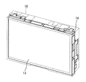
実施形態に係る表示装置の外観を示す斜視図
実施形態における車載装置本体の外観を示す斜視図
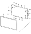
実施形態における表示装置に内蔵された表示パネルユニットおよびフレームを示す斜視図
実施形態における表示装置の一部を分解して示す斜視図
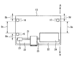
実施形態における表示パネルユニットの背面図
ノイズのシールド効果に関する比較実験結果を示す図であり、図6(a)は接触部を増設していない従来品の測定結果を示し、図6(b)は実施形態の表示装置の測定結果を示す。
比較例を示す図5相当図
比較例を示す図5相当図
以下、一実施形態について図面を参照しながら説明する。図1に示す表示装置10は、例えば車両に搭載されるナビゲーション装置などに備えられ、図2に示す装置本体11の収納部12内に取り付けられるように構成されている。図3に示すように、表示装置10の内部には、フレーム14に取り付けられた表示パネルユニット13が備えられている。表示パネルユニット13とフレーム14との間には、図4に示すように複数のばね15,16,17が介在されている。
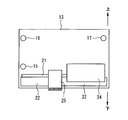
表示パネルユニット13は、液晶の表示パネルユニットで構成されており、詳しい図示は省略するが、2枚のガラス基板の間に液晶を充填し、その背後にバックライトを配置して構成されている。表示パネルユニット13は、図1,図3,図4に示す状態で手前側の面が各種画面を表示する表示面となっている。そして、図5に示すように、表示パネルユニット13は、表示面とは反対側の面である背面側に回路基板部21を備えている。この回路基板部21には、ノイズ発生源である図示しないドライバICやコネクタ基板などの各種電子部品が設けられており、回路基板部21から発生するノイズを遮蔽するためのベース銅箔22によって覆われている。この場合、回路基板部21の一部がベース銅箔22によって覆われている。また、このベース銅箔22には、当該ベース銅箔22に継ぎ足されるようにして回路基板部21を覆う増設銅箔23,24が増設されている。なお、これら増設銅箔23,24の大きさ、形状、位置などは、他の部品との位置関係などに応じて、あるいは、より高いノイズの低減効果を図るために、適宜変更して実施することができる。
また、表示パネルユニット13の背面側には、フレキシブルプリントケーブル25(以下、「FPC25」と称する)が取り付けられている。このFPC25は、例えば複数枚のプラスチックフィルム製のプリント基板を積層して構成した可撓性を有する多層基板からなり、そのほぼ全体に電気絶縁性のコーティングが施されている。このFPC25は、信号線として機能する銅線からなる多数の配線パターンを有しており、例えばハンダ付けなどによって回路基板部21に接続されている。このFPC25もノイズ発生源となり得る。
図4に示すように、フレーム14は、ほぼ矩形状に形成された金属製の部材である。このフレーム14の端部には、複数の取付片部141が一体的に形成されている。また、このフレーム14には、既存の取付片部141に加えて、さらに複数の取付片部142が増設されている。これら取付片部142は、何れも接触部の一例であり、既存の取付片部141の間に存在するスペースなどを利用して設けられる。表示パネルユニット13は、既存の取付片部141および増設された取付片部142に、例えばねじ止めされることにより、あるいは、嵌め込まれることにより、フレーム14に固定される。取付片部142は、例えば表示装置10を構成する他の部品との位置関係などに応じて、あるいは、より高いノイズの低減効果を図るために、表示パネルユニット13の外周部の適宜の位置に接触するように設けられる。また、この取付片部142は、フレーム14に一体的に設けてもよいし、フレーム14とは別の取付部品として設けてもよい。
表示パネルユニット13がフレーム14に支持された状態では、これら表示パネルユニット13とフレーム14との間に隙間が形成されており、本実施形態では、この隙間に、3つのばね15,16,17が挟み込まれている。なお、このフレーム14は、図1に示す表示装置10の金属製の筺体101に直接的あるいは間接的に接続された状態で固定され、これにより、接地電位で維持されるようになっている。ばね15,16,17は、何れも接触部の一例であり、金属により構成されている。これらばね15,16,17は、表示パネルユニット13とフレーム14との間に取り付けられる前の状態で、その伸縮方向である長手方向の寸法が、表示パネルユニット13とフレーム14との間の寸法よりも長くなるように設計されている。従って、これらばね15,16,17は、表示パネルユニット13とフレーム14との間に取り付けられた状態では、その長手方向に沿って圧縮された状態となる。これにより、ばね15,16,17は、表示パネルユニット13とフレーム14との間に取り付けられた状態では、その付勢力によって、表示パネルユニット13の背面およびフレーム14の前面の双方に密着した状態となる。
図5に示すように、ばね15,16,17は、例えば表示装置10を構成する他の部品との位置関係などに応じて、あるいは、より高いノイズの低減効果を図るために、それぞれ異なる位置に配置される。ここで、本実施形態におけるばね15,16,17の配置位置について説明する。なお、以下の説明では、表示パネルユニット13を内蔵する表示装置10が装置本体11に取り付けられた状態で当該表示パネルユニット13の上側に向かう方向(図中の矢印参照)を上方、下側に向かう方向(図中の矢印参照)を下方とする。
即ち、この場合、ばね15は、回路基板部21を覆う増設銅箔23の近傍において、当該増設銅箔23から上方に所定距離Daを有した位置に配置されている。ばね16は、表示パネルユニット13の背面上部において、当該表示パネルユニット13の上側の端部となる上辺から下方に所定距離Dbを有した位置に配置されている。また、このばね16は、ばね15から上方に所定距離Dcを有した位置に配置されている。ばね17は、表示パネルユニット13の背面上部において、当該表示パネルユニット13の上側の端部となる上辺から下方に所定距離Ddを有した位置に配置されている。また、このばね17は、回路基板部21を覆う増設銅箔24の近傍において、当該増設銅箔24から上方に所定距離Deを有した位置に配置されている。なお、複数のばね15,16,17の配置位置を決める所定距離Da~Deは、例えば他の部品との位置関係などに応じて、あるいは、より高いノイズの低減効果を図るために、適宜変更して実施することができる。また、所定距離Dbと所定距離Ddを同じ距離で設定してもよい。即ち、表示パネルユニット13の上辺からばね16までの距離と表示パネルユニット13の上辺からばね17までの距離を同じ距離で設定してもよい。
上記構成の表示装置10において、ノイズ発生源を有する回路基板部21やFPC25からはノイズが発生する。このノイズによる影響を低減するために、この表示装置10においては、表示パネルユニット13とフレーム14との間に複数のばね15,16,17が増設されている。この構成によれば、表示パネルユニット13およびフレーム14は、取付片部141を介して相互に接触することに加えて、さらに、ばね15,16,17を介しても相互に接触する。このため、ノイズ発生源を有する表示パネルユニット13と接地電位に維持されるフレーム14とが接触する部分が増加し、表示パネルユニット13から発生するノイズが既存の接触部および増設された接触部を介してフレーム14に流れやすくなる。従って、ノイズ発生源から発生するノイズの影響を低減することができる。
ここで、本実施形態では、弾性部材であるばね15,16,17を用いているので、ばね15,16,17が表示パネルユニット13およびフレーム14の双方に密着した状態で接触し、表示パネルユニット13およびフレーム14に対するばね15,16,17の接触が不十分となることがない。これによって、表示パネルユニット13から発生するノイズをばね15,16,17を介して確実にフレーム14に流すことができる。さらに、表示装置10によれば、ばね15は、ノイズ発生源を有する回路基板部21を覆う増設銅箔23から所定距離Daを有する近傍位置に配置されている。この構成によれば、増設銅箔23が回路基板部21とばね15との間をつなぐノイズの流路として機能するため、より効率良くノイズの影響を低減することができる。
さらに、表示装置10によれば、表示パネルユニット13およびフレーム14は、既存の取付片部141を介して相互に接触することに加えて、さらに、増設された取付片部142を介しても相互に接触する。そのため、表示パネルユニット13とフレーム14とが接触する部分が増加し、表示パネルユニット13から発生するノイズが既存の接触部および増設された接触部を介してフレーム14に流れやすくなる。従って、ノイズ発生源から発生するノイズの影響を低減することができる。
図6は、本実施形態の効果を確認するために、本実施形態に係る表示装置と従来品とについて、入力信号の周波数を種々変えて回路基板部21近傍の電界強度を測定した結果を示す。これら測定結果から明らかなように、本実施形態の表示装置は従来品と比較してノイズの影響が低減されており、特に400~500MHzの帯域において顕著なノイズ低減効果を得ることができた。また、本実施形態に係る表示装置10の発明者等による検証結果によれば、本実施形態の表示装置10において、ノイズの水平方向の成分が従来よりも約4~13dBほど改善し、ノイズの垂直方向の成分が従来よりも約3~10dBほど改善したことが確認された。
図7は、表示パネルユニット13の背面上部に配置されるばね16,17を、当該表示パネルユニット13の上辺から下方に所定距離を有した位置ではなく、当該表示パネルユニット13の上辺に沿って配置した比較例を示す。この例では、ノイズの水平方向の成分が従来よりも約3~10dBほど改善し、ノイズの垂直方向の成分が従来よりも約3~7dBほど改善したことが確認された。この構成例によっても、ノイズの低減効果を得ることができた。しかし、より高いノイズの低減効果を得るためには、図5に示すように、表示パネルユニット13の上端部に配置されるばね16,17を、当該表示パネルユニット13の上辺から下方に所定距離を有する位置に配置するとよい。なお、この図7に示す例も、本開示の概念に含まれる構成例である。
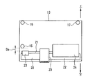
図8は、図5に示す本実施形態の構成から増設銅箔23を除去した比較例を示す。この例では、ノイズの水平方向の成分のうち比較的低い帯域では従来よりも約4~7dBほど改善したが、比較的高い帯域では従来よりも5~10dBほど悪化したことが確認された。また、ノイズの垂直方向の成分が従来よりも約3~4dBほど悪化したことが確認された。よって、より高いノイズの低減効果を得るためには、図5に示すように、増設銅箔を設ければよい。なお、この図8に示す例も、本開示の概念に含まれる構成例である。
また、本開示は、上述した実施形態に限定されるものではなく、その要旨を逸脱しない範囲で種々の実施形態に適用することができる。例えば、表示パネルユニット13は、液晶の表示パネルユニットに限られず、例えば、ELパネル(EL:Electro Luminescence)、FEDパネル(FED:Field Emission Display)などで構成してもよい。また、ばねの形状、寸法、増設数、増設位置などは適宜変更して実施することができる。また、取付片部の形状、寸法、増設数、増設位置などは適宜変更して実施することができる。また、フレーム14の外周部の全周あるいは一部に取付片部を連続的に増設してもよい。また、ノイズ低減対策として、ばねのみを増設した構成としてもよいし、取付片部のみを増設した構成としてもよい。なお、発明者等による検証結果によれば、ノイズ低減対策として取付片部のみを増設した構成においても、ノイズの水平方向の成分が従来よりも約3~6dBほど改善したことが確認された。
本開示は、実施例に準拠して記述されたが、本開示は当該実施例や構造に限定されるものではないと理解される。本開示は、様々な変形例や均等範囲内の変形をも包含する。加えて、様々な組み合わせや形態、さらには、それらに一要素のみ、それ以上、あるいはそれ以下、を含む他の組み合わせや形態をも、本開示の範疇や思想範囲に入るものである。
Claims (5)
- ノイズ発生源(21)を有する表示パネルユニット(13)と、前記表示パネルユニット(13)が取り付けられる金属製のフレーム(14)と、を備える表示装置(10)であって、
前記表示パネルユニット(13)は、前記フレーム(14)に設けられた取り付け部(141)に固定されており、
フレーム(14)には、前記取り付け部(141)以外に、前記表示パネルユニット(13)と前記フレーム(14)とを接触させる接触部(15,16,17,142)が設けられていることを特徴とする表示装置。 - 前記接触部(15,16,17,142)として、前記表示パネルユニット(13)と前記フレーム(14)との間にばね(15,16,17)を備えることを特徴とする請求項1に記載の表示装置。
- 前記ばね(15,16,17)は、複数備えられていることを特徴とする請求項2に記載の表示装置。
- 前記表示パネルユニット(13)には、前記ノイズ発生源(21)を覆う銅箔(23,24)が設けられており、
前記ばね(15,17)は、前記銅箔(23,24)から所定距離を有する位置に配置されていることを特徴とする請求項2または3に記載の表示装置。 - 表示装置(10)は装置本体(11)に取り付けられ、前記ばね(16,17)は、前記表示パネルユニット(13)が前記装置本体(11)に取り付けられた状態で当該表示パネルユニット(13)の上側の端部となる上辺から所定距離を有する位置に配置されていることを特徴とする請求項2から4の何れか1項に記載の表示装置。
Priority Applications (1)
| Application Number | Priority Date | Filing Date | Title |
|---|---|---|---|
| US14/895,002 US9961810B2 (en) | 2013-06-07 | 2014-05-29 | Display device |
Applications Claiming Priority (2)
| Application Number | Priority Date | Filing Date | Title |
|---|---|---|---|
| JP2013-120820 | 2013-06-07 | ||
| JP2013120820A JP6236892B2 (ja) | 2013-06-07 | 2013-06-07 | 表示装置 |
Publications (1)
| Publication Number | Publication Date |
|---|---|
| WO2014196173A1 true WO2014196173A1 (ja) | 2014-12-11 |
Family
ID=52007830
Family Applications (1)
| Application Number | Title | Priority Date | Filing Date |
|---|---|---|---|
| PCT/JP2014/002849 Ceased WO2014196173A1 (ja) | 2013-06-07 | 2014-05-29 | 表示装置 |
Country Status (3)
| Country | Link |
|---|---|
| US (1) | US9961810B2 (ja) |
| JP (1) | JP6236892B2 (ja) |
| WO (1) | WO2014196173A1 (ja) |
Families Citing this family (2)
| Publication number | Priority date | Publication date | Assignee | Title |
|---|---|---|---|---|
| US9736925B2 (en) * | 2014-01-31 | 2017-08-15 | Stmicroelectronics S.R.L. | Packaged semiconductor device having a shielding against electromagnetic interference and manufacturing process thereof |
| JP7100559B2 (ja) * | 2018-10-25 | 2022-07-13 | 株式会社ジャパンディスプレイ | 表示装置 |
Citations (5)
| Publication number | Priority date | Publication date | Assignee | Title |
|---|---|---|---|---|
| JPH11298182A (ja) * | 1998-04-10 | 1999-10-29 | Canon Inc | 電子機器 |
| JP2002215052A (ja) * | 2001-01-23 | 2002-07-31 | Matsushita Electric Ind Co Ltd | 表示装置 |
| JP2006003862A (ja) * | 2004-04-26 | 2006-01-05 | Hitachi Ltd | プラズマディスプレイ装置 |
| JP2011022381A (ja) * | 2009-07-16 | 2011-02-03 | Panasonic Corp | ディスプレイ装置 |
| JP2011253996A (ja) * | 2010-06-03 | 2011-12-15 | Mitsubishi Electric Corp | シールド装置 |
Family Cites Families (16)
| Publication number | Priority date | Publication date | Assignee | Title |
|---|---|---|---|---|
| JP2691027B2 (ja) | 1989-09-20 | 1997-12-17 | 株式会社日立製作所 | 情報処理装置 |
| JP3127774B2 (ja) * | 1995-03-31 | 2001-01-29 | セイコーエプソン株式会社 | シールド材および液晶表示装置 |
| WO2000026888A1 (en) * | 1998-10-30 | 2000-05-11 | Matsushita Electric Industrial Co., Ltd. | Display device with plasma display panel |
| FI108186B (fi) * | 1999-09-29 | 2001-11-30 | Nokia Mobile Phones Ltd | Näytön kehys, jossa on integroitu ESD-suoja, sekä käyttöliittymärakenne |
| JP2004193082A (ja) * | 2002-12-13 | 2004-07-08 | Nec Saitama Ltd | 電子機器の接地構造、該接地構造を備えた電子機器、及び該電子機器の機能ユニット |
| JP3996535B2 (ja) * | 2003-03-20 | 2007-10-24 | Nec液晶テクノロジー株式会社 | 液晶表示装置 |
| JP4055672B2 (ja) * | 2003-07-31 | 2008-03-05 | 株式会社デンソー | 表示装置 |
| KR100612278B1 (ko) * | 2004-05-18 | 2006-08-11 | 삼성에스디아이 주식회사 | 플라즈마 디스플레이 장치 |
| KR100553211B1 (ko) * | 2004-05-24 | 2006-02-22 | 삼성에스디아이 주식회사 | 플라즈마 디스플레이 장치 |
| KR100846584B1 (ko) * | 2005-02-05 | 2008-07-16 | 삼성에스디아이 주식회사 | 배기관 보호 팁 구조 및 이를 구비한 플라즈마 디스플레이모듈 |
| KR100646563B1 (ko) | 2005-07-04 | 2006-11-14 | 삼성에스디아이 주식회사 | 플라즈마 표시장치 |
| JP2008058595A (ja) * | 2006-08-31 | 2008-03-13 | Fujitsu Hitachi Plasma Display Ltd | 表示パネルモジュール及びその製造方法 |
| KR101222576B1 (ko) * | 2006-10-25 | 2013-01-16 | 삼성전자주식회사 | 플라즈마 디스플레이장치 |
| CN101295088B (zh) * | 2007-04-25 | 2011-06-15 | 群康科技(深圳)有限公司 | 液晶显示装置 |
| JP5218367B2 (ja) * | 2009-10-07 | 2013-06-26 | 富士通株式会社 | ケーブル配線構造および電子機器 |
| JP2013101311A (ja) * | 2011-10-12 | 2013-05-23 | Funai Electric Co Ltd | 表示装置およびテレビジョン装置 |
-
2013
- 2013-06-07 JP JP2013120820A patent/JP6236892B2/ja not_active Expired - Fee Related
-
2014
- 2014-05-29 US US14/895,002 patent/US9961810B2/en active Active
- 2014-05-29 WO PCT/JP2014/002849 patent/WO2014196173A1/ja not_active Ceased
Patent Citations (5)
| Publication number | Priority date | Publication date | Assignee | Title |
|---|---|---|---|---|
| JPH11298182A (ja) * | 1998-04-10 | 1999-10-29 | Canon Inc | 電子機器 |
| JP2002215052A (ja) * | 2001-01-23 | 2002-07-31 | Matsushita Electric Ind Co Ltd | 表示装置 |
| JP2006003862A (ja) * | 2004-04-26 | 2006-01-05 | Hitachi Ltd | プラズマディスプレイ装置 |
| JP2011022381A (ja) * | 2009-07-16 | 2011-02-03 | Panasonic Corp | ディスプレイ装置 |
| JP2011253996A (ja) * | 2010-06-03 | 2011-12-15 | Mitsubishi Electric Corp | シールド装置 |
Also Published As
| Publication number | Publication date |
|---|---|
| US20160120076A1 (en) | 2016-04-28 |
| US9961810B2 (en) | 2018-05-01 |
| JP2014239148A (ja) | 2014-12-18 |
| JP6236892B2 (ja) | 2017-11-29 |
Similar Documents
| Publication | Publication Date | Title |
|---|---|---|
| JP6322951B2 (ja) | 車両電子装置 | |
| KR101084201B1 (ko) | 액정 표시 장치 | |
| CN209674745U (zh) | 显示装置 | |
| US11546988B2 (en) | Display device and printed circuit board | |
| CN106028769A (zh) | 显示面板以及显示终端 | |
| CN106664786B (zh) | 静电浪涌防止构造 | |
| JP6236892B2 (ja) | 表示装置 | |
| CN104956425B (zh) | 显示装置 | |
| KR102665517B1 (ko) | 커버 쉴드 및 그를 포함하는 표시 장치 | |
| JP5968266B2 (ja) | 表示装置 | |
| JP2017161792A (ja) | 表示装置 | |
| JP5510391B2 (ja) | 電気回路装置 | |
| JP5161993B2 (ja) | 電子機器 | |
| KR20150015116A (ko) | 전기적 연결 장치를 갖는 전자 장치 | |
| JP6384311B2 (ja) | 表示装置 | |
| JP2016118641A (ja) | 表示装置 | |
| JP2020042141A (ja) | 表示装置 | |
| JP2008211033A (ja) | 表示装置 | |
| JP2015028992A (ja) | 回路基板の接続構造 | |
| KR101549967B1 (ko) | 모니터용 케이스 구조물 | |
| WO2014208439A1 (ja) | 回路基板の接続構造 | |
| JP2013235152A (ja) | 画像表示パネル用fpc | |
| JP2014194491A (ja) | 電子機器 | |
| JP2007298728A (ja) | 表示装置 | |
| JP2015023155A (ja) | 回路基板の接続構造 |
Legal Events
| Date | Code | Title | Description |
|---|---|---|---|
| 121 | Ep: the epo has been informed by wipo that ep was designated in this application |
Ref document number: 14808323 Country of ref document: EP Kind code of ref document: A1 |
|
| WWE | Wipo information: entry into national phase |
Ref document number: 14895002 Country of ref document: US |
|
| NENP | Non-entry into the national phase |
Ref country code: DE |
|
| 122 | Ep: pct application non-entry in european phase |
Ref document number: 14808323 Country of ref document: EP Kind code of ref document: A1 |