WO2014185293A1 - コンデンサのシミュレーション方法およびコンデンサの非線形等価回路モデル - Google Patents
コンデンサのシミュレーション方法およびコンデンサの非線形等価回路モデル Download PDFInfo
- Publication number
- WO2014185293A1 WO2014185293A1 PCT/JP2014/062156 JP2014062156W WO2014185293A1 WO 2014185293 A1 WO2014185293 A1 WO 2014185293A1 JP 2014062156 W JP2014062156 W JP 2014062156W WO 2014185293 A1 WO2014185293 A1 WO 2014185293A1
- Authority
- WO
- WIPO (PCT)
- Prior art keywords
- voltage
- capacitor
- vdc
- equivalent circuit
- current
- Prior art date
- Legal status (The legal status is an assumption and is not a legal conclusion. Google has not performed a legal analysis and makes no representation as to the accuracy of the status listed.)
- Ceased
Links
Images






Classifications
-
- G—PHYSICS
- G06—COMPUTING OR CALCULATING; COUNTING
- G06F—ELECTRIC DIGITAL DATA PROCESSING
- G06F30/00—Computer-aided design [CAD]
- G06F30/30—Circuit design
- G06F30/36—Circuit design at the analogue level
- G06F30/367—Design verification, e.g. using simulation, simulation program with integrated circuit emphasis [SPICE], direct methods or relaxation methods
-
- G—PHYSICS
- G06—COMPUTING OR CALCULATING; COUNTING
- G06F—ELECTRIC DIGITAL DATA PROCESSING
- G06F17/00—Digital computing or data processing equipment or methods, specially adapted for specific functions
- G06F17/10—Complex mathematical operations
Definitions
- the present invention relates to a capacitor simulation method for simulating nonlinear characteristics when a DC voltage is applied to a capacitor, and a nonlinear equivalent circuit model of the capacitor used for the simulation.
- this kind of electronic component simulation method and equivalent circuit model are used for circuit simulation in electronic circuit design.
- a circuit simulator such as SPICE (Simulation Program with Integrated Circuit Circuit) is used, and some circuit simulators can be used on a website of an electronic component manufacturer.
- SPICE Simulation Program with Integrated Circuit Circuit
- a user accesses a homepage site of an electronic component manufacturer through a network from a terminal such as a personal computer and uses a circuit simulator.
- Patent Document 1 Conventionally, as this kind of simulation method and equivalent circuit model, for example, there is a capacitor disclosed in Patent Document 1.
- a given frequency characteristic of a capacitor is input, and in a second step, a frequency-independent resistance (R) and capacitance (C ), An RC circuit, an RL circuit, and an RCL circuit are formed as an equivalent circuit model as a circuit that can be simulated in the time domain using the inductance (L).
- R frequency-independent resistance
- C capacitance
- An RC circuit, an RL circuit, and an RCL circuit are formed as an equivalent circuit model as a circuit that can be simulated in the time domain using the inductance (L).
- an evaluation function for determining the accuracy of the equivalent circuit model formed in the second step is synthesized, and in the fourth step, the evaluation function synthesized in the third step is minimized.
- the circuit constant is determined.
- Patent Literature 1 an equivalent circuit model capable of performing simulation in the time domain of a capacitor whose impedance is shown in the frequency domain with the above configuration is derived, and the electrical characteristics of the capacitor in the frequency domain or in the time domain are expressed as follows: Predict by circuit simulation.
- Patent Document 2 Conventionally, as an inductor simulation method and an equivalent circuit model, for example, there is one disclosed in Patent Document 2.
- the mutual inductance Lm between the inductance L0 and the inductance L1 with respect to the direct current is added to the series circuit of the inductance L1 and the resistance R1 considering the skin effect of the inner conductor.
- an equivalent circuit model is used in which an inductance L0 for DC and a DC resistance Rdc1 of the internal conductor are connected in series.
- the inductance and resistance of the external electrode are simultaneously considered, the inductance Ls of the external electrode is connected in series with the inductance L0, and the DC resistance Rdc2 of the external electrode is connected to the DC resistance Rdc1 of the internal conductor.
- a series circuit in which a parasitic capacitance Cp of a dielectric constituting the chip of the multilayer chip inductor and a resistor Rp representing a loss of the dielectric are connected in series is connected in parallel inside the equivalent elements Ls and Rdc2 of the external electrodes. Is done.
- Patent Document 2 an error that occurs between circuit design and actual circuit performance is suppressed by circuit simulation using the above-described equivalent circuit model.
- the ideal C circuit model is represented by an equivalent circuit having one capacitance element C as a circuit element, as shown in FIG.
- the voltage v applied to both ends of the capacitance element C is expressed as follows when the time-varying signal voltage and noise voltage applied to both ends are represented as v ac and the DC bias voltage applied to both ends is represented as V dc. ).
- v v ac + V dc (1)
- an arithmetic circuit is constructed as shown in FIG.
- the capacitance element C is converted into a non-linear voltage control voltage source UA3 controlled by the DC bias voltage Vdc .
- the total voltage v applied across the capacitor passes through the low-pass filters L1 and R1 having extremely low cut-off frequency via the linear voltage control voltage source E1, thereby obtaining the DC bias voltage V dc.
- the non-linear voltage control voltage source UA3 supplied to the non-linear voltage control voltage source UA3.
- the differential voltage dv / dt is performed by supplying the total voltage v to the input terminal of the differential device UA1 through the linear voltage control voltage source E2.
- the output voltage v1 of the differentiation device UA1 is input to the three-terminal multiplication device UA2 together with the output voltage (C (V dc )) of the non-linear voltage control voltage source UA3 substituting the capacitance element C, so that multiplication (C (V dc ) ⁇ dv / dt) is performed.
- the multiplication result is output to the output terminal of the multiplication device UA2. Since the output voltage v2 of the multiplication device UA2 is equal to the product of the current i flowing through the capacitor and the unit resistance, the output voltage v2 is replaced with a capacitor by using the linear voltage control current source G controlled by the output voltage v2.
- Such an ideal C circuit model is not suitable for circuit simulation because the difference from the impedance characteristics of actual parts, especially in the high frequency band, is too large, but it is convenient for the initial stage of circuit design or prediction of circuit characteristics. It is.
- the broadband high-accuracy equivalent circuit model disclosed in Patent Document 3 is applied to MLCC (multilayer ceramic capacitor) simulation.
- MLCC multilayer ceramic capacitor
- FIG. 5B of the same document an equivalent circuit model having a circuit configuration shown in FIG.
- FIG. 5A of the same document considers the thickness of the plurality of internal electrodes 20 of the multilayer chip capacitor 10, and the electromagnetic effect on the upper surface 22 and the lower surface 24 of each of the plurality of internal electrodes 20.
- the electromagnetic effect of one side surface 26 and the other side surface 28 of the plurality of internal electrodes 20 and the open end surface 30 is also taken into consideration.
- the values of various circuit elements in this equivalent circuit are all changed by the DC bias voltage.
- the characteristic change of each circuit element due to the DC bias voltage is expressed by a polynomial, and an equivalent circuit model of MLCC when this characteristic change is expected is shown in FIG.
- a differentiation device in addition to a differentiation device, a multiplication device, a 3-terminal or 4-terminal addition device, a division device and a 5-terminal addition device are also used.
- Such a broadband high-accuracy model that anticipates a characteristic change due to a DC bias voltage can obtain good simulation accuracy in a wide frequency band.
- the approximation formula reflecting the dependence of the DC bias includes an odd-numbered power clause, so that the case where the sign of the DC bias is reversed cannot be dealt with.
- the model has a polarity problem. Further, when the value of the DC bias suddenly changes, there is a problem that the value is converted into a divergent value.
- the present invention has been made to solve such problems,
- the equivalent circuit of the capacitor is expressed using passive circuit elements,
- the characteristic change rate of the passive circuit element when a DC voltage is applied is expressed as an approximate function with the voltage as a variable based on the actual measurement value. Refer to the voltage applied to the capacitor, and apply the DC voltage based on the characteristic change rate calculated by the approximate function corresponding to the referenced voltage and the no-application current that flows to the passive circuit element when no DC voltage is applied.
- the control current source connected in parallel to the passive circuit element with a variable voltage generates a differential current between the applied current and non-applied current flowing in the passive circuit element when a DC voltage is applied, and the differential current is applied to the non-applied current.
- a capacitor simulation method that simulates the nonlinear characteristics of a capacitor when a DC voltage is applied is constructed.
- a passive circuit element representing an equivalent circuit of a capacitor, Voltage reference means for referring to the voltage applied to the capacitor;
- the characteristic change rate of the passive circuit element when a DC voltage is applied an approximate function that expresses the voltage as a variable based on the actual measurement value, and the characteristic change rate calculated corresponding to the voltage referenced by the voltage reference means, and the DC voltage
- a differential current between the applied current and the non-application current that flows through the passive circuit element when a DC voltage is applied is generated.
- a control current source connected in parallel to the circuit element to form a nonlinear equivalent circuit model of the capacitor.
- the characteristic change rate of the passive circuit element when a DC voltage is applied is expressed by an approximate function using the voltage to be referenced as a variable based on the actual measurement value. . Therefore, the characteristic change rate of the passive circuit element is calculated by this approximate function according to the voltage to be referred to.
- the applied current that flows to the passive circuit element when the DC voltage is applied can be obtained by causing the difference current between the applied current and the non-applied current to flow simultaneously with the non-applied current that flows to the passive circuit element when the DC voltage is not applied, Can be sought.
- the control current source generates a differential current between the application current and non-application current, and a passive circuit element is connected in parallel to the control current source.
- the difference current to the non-application current the application current of the passive circuit element can be simulated.
- the characteristic change rate of the passive circuit element is calculated by an approximation function with reference to the voltage applied to the capacitor, and a differential current is generated by the control current source based on the characteristic change rate and the non-applied current.
- a simulation capable of dynamically following the applied voltage can be performed.
- the nonlinear equivalent circuit model of the capacitor can be obtained by simply causing the differential current to be combined with the non-application current by using the control current source with reference to the non-application current.
- the control current source from the circuit model, it is possible to easily obtain an equivalent circuit model of the capacitor corresponding to the non-application current, that is, when no DC voltage is applied.
- the present invention is characterized in that the approximate function is given as an even function in a polynomial format that does not include an odd-order power term.
- the approximate function is expressed in a polynomial format that does not include an odd-order power term, unlike the conventional capacitor simulation, when the sign of the DC bias is reversed or the value of the DC bias is Even in the case of a sudden change, the characteristic change rate of the passive circuit element is appropriately approximated by an approximation function.
- the present invention is characterized in that the voltage applied to the capacitor is referred to at both ends of the equivalent circuit, and the non-application current is referred to at the input end or output end of the passive circuit element.
- the instantaneous voltage generated at both ends of the circuit in the equivalent circuit model or the passive voltage in the equivalent circuit model is calculated by referring to the instantaneous current generated at the input end or output end of the circuit element. For this reason, the voltage used for the calculation of the differential current and the non-application current are referred to without time delay, and the transient response analysis of the nonlinear characteristics of the capacitor can be performed at high speed and with high accuracy.
- the passive circuit element connected in parallel to the control current source is a capacitive element alone, a parallel circuit of a capacitive element and a resistive element, or a parallel circuit of a capacitive element, a resistive element, and an inductive element. It is characterized by that.
- the characteristics of the passive circuit element when a DC voltage is not applied are represented by the capacitive element alone, the parallel circuit of the capacitive element and the resistive element, or the parallel circuit of the capacitive element, the resistive element, and the inductive element. Is done. And by connecting a control current source in parallel to these circuits, characteristics when a DC voltage of a passive circuit element is applied are simulated.
- the present invention is characterized in that a plurality of parallel circuits of a control current source and passive circuit elements are connected in series.
- the simple parallel circuit of the control current source and the passive circuit element is simply connected in series, and the number of series increases, so that the simulation accuracy of the equivalent circuit model can be improved. Therefore, an equivalent circuit model with high simulation accuracy can be configured regularly and with good visibility. Further, since a plurality of parallel circuits of the control current source and the passive circuit element are simply connected in series, the characteristics of the passive circuit element when a DC voltage is applied can be simulated by a systematic calculation procedure.
- the present invention is characterized in that the equivalent circuit includes a passive circuit element whose characteristics do not change when a DC voltage is applied to the capacitor.
- an equivalent circuit model is configured by combining a passive circuit element whose characteristics are changed by application of a DC voltage and a passive circuit element whose characteristics are not changed by application of a DC voltage.
- the simulation can be made more accurate and the frequency band of the simulation can be widened.
- the present invention also provides: A first step of inputting a capacitor type; A second step of inputting a voltage applied to the capacitor or a current flowing through the capacitor; A characteristic change calculated by referring to the voltage applied to the capacitor by the voltage or current input in the second step and corresponding to the reference voltage by an approximation function prepared in advance for the type of capacitor input in the first step
- the differential current is generated by the control current source based on the rate and the non-application current, and the non-application current is combined with the differential current, thereby simulating the nonlinear characteristic of the capacitor when the DC voltage is applied.
- a computer program that implements any one of the above-described capacitor simulation methods or functions a nonlinear equivalent circuit model of any of the above-described capacitors is configured.
- the type of capacitor to be simulated and the value of the voltage applied to the capacitor or the current flowing to the capacitor are input to the computer program.
- the differential current is caused to flow in parallel with the non-application current of the passive circuit element, and the simulation is automatically performed. Therefore, the user of this simulation method or this nonlinear equivalent circuit model can input the value of the type of capacitor to be simulated and the voltage applied to the capacitor or the current to be passed to the computer program. Can be performed with high accuracy and ease. As a result, even a general user who does not have specialized knowledge about circuit simulation can accurately and easily perform an accurate circuit simulation of an electronic circuit using a capacitor.
- the present invention is configured to use a computer program that accesses a server including the computer program via an Internet network and uses the computer program from a terminal connected to the Internet network.
- the user can easily use the computer program by accessing a server including the computer program from a terminal connected to the Internet network. Therefore, it is possible to provide a large number of users with the capacitor simulation method and the capacitor nonlinear equivalent circuit model according to the present invention.
- the capacitor simulation method and the nonlinear equivalent circuit model of the capacitor that can dynamically simulate the nonlinear characteristics of the capacitor when a DC voltage is applied with high accuracy can be easily obtained. Can be provided.
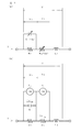
- FIG. (A) is a passive equivalent circuit model when no DC voltage is applied to the capacitor according to the first embodiment of the present invention
- (b) is a nonlinear equivalent circuit model of the capacitor when DC voltage is applied according to the first embodiment
- FIG. (A) is a non-linear equivalent circuit model of a capacitor when a DC voltage is applied, expressed using the variable resistance element R X1 (Vdc) and the variable capacitance element C X1 (Vdc)
- (b) is the first embodiment.
- It is a circuit diagram which shows the nonlinear equivalent circuit model of the capacitor
- (A) is a characteristic calculated from the passive equivalent circuit model shown in FIG. 1 (a), with respect to the frequency characteristic for the magnitude MagZ of the impedance Z of the capacitor calculated from the nonlinear equivalent circuit model shown in FIG. 1 (b).
- the graph shown in comparison with (b) shows the frequency characteristics of the equivalent series resistance ESR of the capacitor calculated from the nonlinear equivalent circuit model shown in FIG. 1 (b), from the passive equivalent circuit model shown in FIG. 1 (a). It is a graph shown in comparison with the calculated characteristic.
- (A) is a passive equivalent circuit model when no DC voltage is applied to the capacitor according to the second embodiment of the present invention
- (b) is a nonlinear equivalent circuit of the capacitor when DC voltage is applied according to the second embodiment.
- FIG. 4B is a graph showing the frequency characteristics of the equivalent series resistance ESR of the capacitor calculated from the nonlinear equivalent circuit model shown in FIG. 4B, from the passive equivalent circuit model shown in FIG. It is a graph shown in comparison with the calculated characteristic.
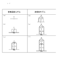
- (A), (b), (c) are passive circuit elements that are used in the passive equivalent circuit model in each embodiment of the present invention and represent characteristics when the DC voltage Vdc is not applied
- (d), (d) e) and (f) are diagrams showing a configuration of a passive circuit element representing a nonlinear characteristic when a DC voltage Vdc is applied, which is used in the nonlinear equivalent circuit model in each embodiment.
- (A) is an impedance expansion type passive equivalent circuit model including passive circuit elements r, c and l whose characteristics are not changed by application of the DC voltage Vdc to the capacitor, and (b) is the passive circuit element r.
- C, l is a circuit diagram showing an impedance expansion type nonlinear equivalent circuit model configured to include. It is a circuit diagram of the nonlinear equivalent circuit model in the 3rd Embodiment of this invention which represented the nonlinear equivalent circuit model shown in FIG.8 (b) in general form.
- FIG. 10 is a circuit diagram showing a specific example of an impedance expansion type equivalent circuit model of a capacitor according to a fourth embodiment of the present invention, which is configured by combining passive circuit elements whose characteristics are not changed by application of a DC voltage Vdc. .
- FIG. 10 is a graph showing the calculated values calculated using the equivalent circuit model shown in FIG. 10 for the magnitude ZZ of the capacitor impedance Z and the equivalent series resistance ESR when no DC voltage Vdc is applied in comparison with the measured values. is there. It is a circuit diagram for demonstrating the application rule used when correct
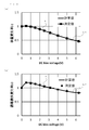
- (A) is a graph showing the capacitance change rate kc of the capacitor as an approximate function of the DC voltage Vdc applied to the capacitor, and (b) is the DC voltage applied to the capacitor. It is a graph represented as an approximate function of Vdc.
- (A) is a passive equivalent circuit model when no DC voltage is applied to the capacitor in the fourth embodiment, based on the equivalent circuit model shown in FIG. 10, and (b) is also based on the equivalent circuit model shown in FIG.
- FIG. 10 is a circuit diagram showing a nonlinear equivalent circuit model of a capacitor when a DC voltage is applied in the fourth embodiment.
- (A) is a graph showing the calculated value calculated using the equivalent circuit model shown in FIG. 14 with respect to the magnitude MagZ of the impedance Z of the capacitor, and (b) is the equivalent series resistance of the capacitor. It is a graph which compares the calculated value calculated using the equivalent circuit model shown in FIG. 14, and measured value about ESR.
- FIG. 1A is a passive equivalent circuit model when no DC voltage is applied to the capacitor in the first embodiment
- FIG. 1B is a nonlinear equivalent circuit of the capacitor when DC voltage is applied in the first embodiment. It is a circuit diagram which shows a model.
- the series circuit of the resistance element R 1 and the capacitor element C 1 constitute a passive circuit elements representing an equivalent circuit of a capacitor as a target of simulation.
- an AC voltage Vac on which no DC voltage Vdc is superimposed is applied as a voltage V to the passive circuit elements R 1 and C 1 by the LTspice voltage source model V 0 .
- an AC voltage Vac superimposed with a DC voltage Vdc is applied as a voltage V to the passive circuit elements L 1 and R 1 by the LTspice voltage source model V 1 .
- the circuit constant of the capacitive element C 1 in each equivalent circuit was set to 8 [ ⁇ F]
- the circuit constant of the resistance element R 1 was set to 2.5 [m ⁇ ]
- the DC applied voltage Vdc was set to 6 [V].
- These voltage source models V n0 , V n1 , V R1 , and V C1 are components for convenience in LTspice set in order to measure the current at each location, and the set voltage V is set to 0 [V]. Used as an ammeter.
- the control current sources B R1 and B C1 shown in FIG. 5B are circuit constant change rates of the passive circuit elements R 1 and C 1 , that is, characteristic change rates k R1 (Vdc) and k C1 (Vdc), and no application
- characteristic change rates k R1 (Vdc) and k C1 (Vdc) and no application
- differential currents ⁇ I R1 and ⁇ I C1 between the applied currents I R1 (Vdc) and I C1 (Vdc) and the no-application currents I R1 and I C1 are obtained. generate.
- Non-application time of the current I R1, I C1 is the voltage source model V R1, V C1, but is referenced at the input of the passive circuit elements R 1, C 1, at the output of passive circuit elements R 1, C 1 You may make it refer.
- the characteristic change rates k C1 (Vdc) and k R1 (Vdc) are the circuit constants when the DC voltage Vdc is applied to the circuit constants of the passive circuit elements R 1 and C 1 when the DC voltage Vdc is not applied. Is the ratio.
- the non-application currents I R1 and I C1 are currents that flow through the passive circuit elements R 1 and C 1 when the DC voltage Vdc is not applied.
- the application currents I R1 (Vdc) and I C1 (Vdc) are This is the current that flows through the passive circuit elements R 1 and C 1 when the DC voltage Vdc is applied. As shown in the figure, these control current sources B R1 and B C1 are connected in parallel to passive circuit elements R 1 and C 1 whose characteristics are changed by application of a DC voltage Vdc.
- the passive circuit elements R 1 and C 1 in each equivalent circuit model represent invariable ones whose circuit constants do not depend on the DC applied voltage Vdc, and the voltage fluctuations due to the characteristic changes are the control current sources B R1 and B C1.
- the control current sources B R1 and B C1 are components of LTspice treated as a behavioral current source model in LTspice, and their own values depend on the voltage Vref to be referenced and the non-application currents I R1 and I C1. To be determined.
- the voltage V applied across the capacitor by the voltage source models V 0 and V 1 is referred to by the control current sources B R1 and B C1
- the DC voltage Vdc of the voltage V is the reference voltage Vref.
- the control current sources B R1 and B C1 constitute voltage reference means for referring to the voltage Vref applied to the capacitor to be simulated.
- the reference voltage Vref may be referred to with reference to both the DC voltage Vdc and the AC voltage Vac.
- the capacitive element C 1 is applied DC voltage
- the variable capacitance element C X1 (Vdc) whose resistance value varies depending on the value of Vdc, and the resistance element R 1 are variable resistance elements R X1 (Vdc) whose resistance value varies depending on the value of the DC applied voltage Vdc.
- a resistive element R 2 is connected in parallel to the capacitive element C 1
- a variable resistive element R X1 (Vdc) and an inductive element L 2 are connected in series.
- V V 1 + V 2
- I V 1 / R 2 + C X1 (Vdc) ⁇ dV 1 / dt ... (5)
- I V 2 / R X1 (Vdc) (6)
- variable capacitance element C X1 (Vdc) whose circuit constant is changed by the application of the DC voltage Vdc is controlled by the control current source B C treated as a behavioral current source model in LTspice as shown in FIG. and expressed as a parallel circuit of a capacitor C 1.
- the variable resistor element R X1 (Vdc) which changes the circuit constant by application of the DC voltage Vdc, as shown in FIG. 2 (b), the control current source B R and the resistor element to be treated as behavioral source model in LTspice It expressed as a parallel circuit of R 1.
- the capacitive element C 1 and the resistive element R 1 are the same as those in FIG. 1, and represent circuit elements whose circuit constants do not depend on the DC applied voltage Vdc.
- Controlled current source B C is the variation of the current generated in the capacitor C 1 by application of the DC voltage Vdc, is generated as differential current [Delta] I C1 according to the value of the applied DC voltage Vdc (Vdc).
- Controlled current source B R is the variation of the current generated in the resistor element R 1 by application of the DC voltage Vdc, it is generated as differential current ⁇ I R1 (Vdc) according to the value of the DC voltage Vdc.
- the equivalent capacitance model of the variable capacitance element C X1 (Vdc) and the variable resistance element R X1 (Vdc) is converted into the equivalent model as described above, so that the circuit shown in FIG. It is replaced with the nonlinear equivalent circuit model of this embodiment shown. That is, the series circuit of the variable capacitance element C X1 (Vdc) and the variable resistance element R X1 (Vdc) shown in FIG. 2A has a control current source BC and a capacitance as shown in FIG. A circuit in which a parallel circuit of a control current source BR and a resistance element R 1 is connected in series to a parallel circuit of the element C 1 is replaced.
- the characteristic change rate k C1 (Vdc) is for circuit constants C 1 of passive circuit elements C 1 at the time of no application of the DC voltage Vdc, the ratio of the circuit constants C X1 is supplied, the DC voltage Vdc (Vdc) Yes, it is expressed by the following equation (10).
- k C1 (Vdc) C X1 (Vdc) / C 1 (10)
- control current source B C multiplies the value obtained by subtracting 1 from the characteristic change rate k C1 (Vdc) by the non-application current I C1 , that is, the characteristic change rate k. based on C1 (Vdc) and non-application time of the current I C1, to generate a differential current ⁇ I C1 (Vdc) applied when current I C1 and (Vdc) and application of no voltage when current I C1.
- Controlled current source B R by multiplying the non-application time of the current I R1 to the value obtained by subtracting 1 from the inverse of (11) as shown in the formula, characteristic change rate k R1 (Vdc), that is, the characteristic change based on the rate k R1 (Vdc) and non-application time of the current I R1, applied during current I R1 (Vdc) and to generate a differential current ⁇ I R1 (Vdc) of the non-application time of the current I R1.
- characteristic change rate k R1 (Vdc) that is, the characteristic change based on the rate k R1 (Vdc) and non-application time of the current I R1, applied during current I R1 (Vdc) and to generate a differential current ⁇ I R1 (Vdc) of the non-application time of the current I R1.
- the approximate function exp (f (x)) is expressed as described later (see FIG. 13) using the reference voltage Vref applied to the capacitor as a variable x based on the actually measured value.
- the approximate function exp (f (x)) is given as an even function in a polynomial format that does not include an odd-order power term.
- an equivalent circuit of the capacitor is represented by using a series circuit of passive circuit elements R 1 and C 1 , and a nonlinear equivalent circuit model shown in FIG. 1B is constructed. Then, an approximate function using the reference voltage Vref as a variable x based on the actual measurement values of the characteristic change rates k R1 (Vdc) and k C1 (Vdc) of the passive circuit elements R 1 and C 1 when the DC voltage Vdc is applied. Express as exp (f (x)). Next, the reference voltage Vref is referred to by the control current sources B R1 and B C1 connected in parallel to the passive circuit elements R 1 and C 1 , and the approximate function exp (f (x)) is used to obtain the reference voltage.
- Characteristic change rates k R1 (Vdc) and k C1 (Vdc) are calculated corresponding to Vref. Further, the passive circuit elements R 1, non-application time of the current flowing through the C 1 I R1, I C1 as measured by a voltage source model V R1, V C1, referred to by the control current source B R1, B C1. Based on the characteristic change rates k R1 (Vdc), k C1 (Vdc) and the non-application currents I R1 , I C1 , the application currents I R1 (Vdc), I C1 are controlled by the control current sources B R1 , B C1.
- FIG. 3A shows the frequency characteristic of the magnitude MagZ of the impedance Z of the capacitor calculated from the nonlinear equivalent circuit model shown in FIG. It is a graph which compares and shows the frequency characteristic about the same magnitude
- the horizontal axis of the graph represents the frequency [Hz], and the vertical axis represents the value [ ⁇ ] of the magnitude MagZ.
- FIG. 3B shows the frequency characteristic of the equivalent series resistance ESR of the capacitor calculated from the nonlinear equivalent circuit model shown in FIG. 1B when the nonlinear characteristic of the capacitor is simulated as described above. It is a graph which compares and shows the frequency characteristic about the equivalent series resistance ESR calculated from the passive equivalent circuit model shown to a). The horizontal axis of the graph represents the frequency [Hz], and the vertical axis represents the value [ ⁇ ] of the equivalent series resistance ESR.
- the frequency characteristic A1 for the magnitude MagZ of the impedance is such that the value of MagZ is greater than the frequency characteristic A0 when no DC voltage is applied by applying the DC voltage Vdc,
- the impedance fluctuates due to the application of the DC voltage Vdc.
- the characteristics of the equivalent series resistance ESR shown in FIG. in the high frequency range, the characteristics of the equivalent series resistance ESR shown in FIG.
- the frequency characteristic B1 for the equivalent series resistance ESR is also greater than the frequency characteristic B0 when the DC voltage Vdc is not applied due to the application of the DC voltage Vdc. It fluctuates due to the application of the DC voltage Vdc.
- the value of the equivalent series resistance ESR is a constant value regardless of the frequency.
- k C1 (Vdc) is represented by an approximate function exp (f (x)) with the reference voltage Vref applied to the capacitor as a variable x based on the actually measured value. Therefore, the characteristic change rates k R1 (Vdc) and k C1 (Vdc) shown in the equations (10) and (12) are calculated by this approximate function exp (f (x)) according to the voltage Vref to be referred to. Is done.
- the applied currents I R1 (Vdc) and I C1 (Vdc) are the non-applied currents I R1 and I C1 , and the differential currents ⁇ I R1 (Vdc) and ⁇ I shown in the equations (9) and (11), respectively. It can be obtained by co-flowing C1 (Vdc). Therefore, based on the characteristic change rates k R1 (Vdc) and k C1 (Vdc) and the non-application currents I R1 and I C1 , the differential current ⁇ I R1 (Vdc) is generated by the control current sources B R and B C.
- ⁇ I C1 (Vdc) passive circuit elements R 1 , C 1 are connected in parallel to the control current sources B R , B C , and the differential currents ⁇ I R1 (Vdc), ⁇ I C1 (Vdc) are not marked.
- the pressure during the current I R1, I C1 be to cocurrent
- passive circuit elements R 1, C 1 of the application time of the current I R1 (Vdc) can be simulated I C1 and (Vdc).
- the characteristic change rates k R1 (Vdc) and k C1 (Vdc) of the passive circuit elements R 1 and C 1 are calculated by the approximation function exp (f (x)) with reference to the voltage Vref applied to the capacitor, and the characteristic change Based on the ratios k R1 (Vdc), k C1 (Vdc) and the non-application currents I R1 , I C1 , the control current sources B R , B C give the differential current ⁇ I R1 shown in the formulas (9) and (11).
- (Vdc), ⁇ I C1 (Vdc) it is possible to perform a simulation capable of dynamically following an arbitrary DC applied voltage Vdc.
- non-linear equivalent circuit model of the capacitor as described above, non-application time of the current I R1, I C1 based on the, non-application time of the current I R1, I C1 to the differential current ⁇ I R1 (Vdc), ⁇ I C1 ( Vdc) can be obtained by simply causing the control current sources B R and B C to simultaneously flow, and conversely, by excluding the control current sources B R and B C from the nonlinear equivalent circuit model shown in FIG.
- the equivalent circuit model of the capacitor shown in FIG. 1A corresponding to the non-application currents I R1 and I C1 that is, when the DC voltage Vdc is not applied, can be easily obtained.
- the approximate function exp (f (x)) is expressed by an even function of a polynomial form that does not include an odd-order power term. Therefore, unlike the conventional capacitor simulation, the characteristic change rates k R1 (Vdc), k C1 (when the sign of the DC bias is reversed or when the value of the DC bias changes suddenly, etc. Vdc) is appropriately approximated by an approximation function exp (f (x)).
- the reference voltage Vref or non-application currents I R1 and I C1 are set separately from the equivalent circuit model and calculated.
- the instantaneous voltage generated at both ends of the circuit in the equivalent circuit model or the instantaneous current generated at the input terminal or output terminal of the passive circuit elements R 1 and C 1 in the equivalent circuit model is referred to, and the differential current ⁇ I R1 (Vdc ), ⁇ I C1 (Vdc) is calculated.
- the reference voltage Vref used in the calculation of the differential currents ⁇ I R1 (Vdc) and ⁇ I C1 (Vdc) and the non-application currents I R1 and I C1 are referred to without time delay, and a transient response analysis of the nonlinear characteristics of the capacitor is performed. Can be performed at high speed and with high accuracy.
- FIG. 4A shows a passive equivalent circuit model when no DC voltage is applied to the capacitor according to the second embodiment of the present invention
- FIG. 4B shows a capacitor when DC voltage is applied according to the second embodiment.
- It is a circuit diagram which shows the nonlinear equivalent circuit model of. In the figure, the same or corresponding parts as in FIG.
- a parallel circuit of the capacitive element C 2 and the resistive element R 2 is connected in series with the series circuit of the resistive element R 1 and the capacitive element C 1.
- a passive circuit element representing an equivalent circuit of a capacitor to be simulated is configured.
- the resistive element R 2 is a resistive element whose circuit constant does not depend on the DC applied voltage Vdc. in parallel with R 2, a control current source B R which is treated as a behavioral current source model is connected.
- the capacitive element C 2 the control current source B C where the circuit constant is treated as a behavioral source model in parallel with the capacitive element C 2, which does not depend on the applied DC voltage Vdc is connected.
- these controlled current source B R and B C are connected in parallel, as shown in FIG. 5 (b), it can be expressed as one of the control current source (B R + B C).
- the current value generated by the controlled current source (B R + B C) is the sum of the values of the currents each control current source B C and B R are generated.
- control current source B R1 is connected in parallel to the resistor element R 1
- control current source B C1 , the capacitor element C 2 and the resistor element R 2 are connected in parallel to the capacitor element C 1.
- a control current source B C2 corresponding to the control current source (B R + B C ) shown in FIG. 5B is connected in parallel with the parallel circuit. That is, in each equivalent circuit model in the second embodiment, the parallel circuit of the control current source B R1 and the passive circuit element R 1 , the parallel circuit of the control current source B C1 and the passive circuit element C 1 , and the control current A plurality of the source B C2 and the parallel circuit of the passive circuit elements C 2 and R 2 are connected in series.
- the passive equivalent circuit model shown in FIG. 4 (a) the AC voltage Vac to DC voltage Vdc is not applied, as a voltage V across the equivalent circuit by a voltage source model V 0 Applied.
- the AC voltage Vac to DC voltage Vdc is applied, it is applied to both ends of the equivalent circuit by a voltage source model V 1 as the voltage V.
- the circuit constant of the capacitive element C 1 in each equivalent circuit is 8 [ ⁇ F]
- the circuit constant of the resistive element R 1 is 2.5 [m ⁇ ]
- the circuit constant of the capacitive element C 2 is 1 [mF]
- the resistive element circuit constants of R 2 is 10 [m ⁇ ]
- the DC voltage applied Vdc was set to 6 [V].
- the control current source B R1 shown in FIG. 4B is based on the characteristic change rate k R1 (Vdc) of the resistance element R 1 and the non-application current I R1 , as in the simulation method of the first embodiment. resistive elements R 1 applied during the current I R1 (Vdc) and to generate a differential current ⁇ I R1 (Vdc) of the non-application time of the current I R1.
- controlled current source B C based on the capacitive element C 1 characteristic change rate k C1 (Vdc) and non-application time of the current I C1, similarly to the control current source B R1, applied during current of the capacitor C 1 I C1 (Vdc) and to generate a difference current [Delta] I C1 of the non-application time of the current I C1 (Vdc).
- controlled current source B C2 the capacitance element C 2 of the characteristic change rate k C2 (Vdc) and a resistor R 2 of characteristic change rate k R2 (Vdc), and, no application during current of the capacitor C 2 I C2 and based on the non-application time of the current I R2 of the resistance element R 2, upon application of the capacitive element C 2 current I C1 and (Vdc) and the difference current [Delta] I C1 of the non-application time of the current I C1 (Vdc), the resistance element generating an R applied during current I R2 of the 2 (Vdc) and application of no voltage when current I R2 and the differential current ⁇ I R1 (Vdc) and the difference current [Delta] I C1 in conjunction with (Vdc) + ⁇ I R1 (Vdc ).
- 6A is calculated from the frequency characteristic of the magnitude MagZ of the impedance Z of the capacitor calculated from the nonlinear equivalent circuit model shown in FIG. 4B and the passive equivalent circuit model shown in FIG. It is a graph which compares and shows the frequency characteristic about the same magnitude
- the horizontal axis of the graph represents the frequency [Hz], and the vertical axis represents the value [ ⁇ ] of the magnitude MagZ.
- FIG. 6B shows the frequency characteristic of the equivalent series resistance ESR of the capacitor calculated from the nonlinear equivalent circuit model shown in FIG. 4B and the same equivalent calculated from the passive equivalent circuit model shown in FIG. It is a graph which compares and shows the frequency characteristic about series resistance ESR.
- the horizontal axis of the graph represents the frequency [Hz], and the vertical axis represents the value [ ⁇ ] of the equivalent series resistance ESR.
- the frequency characteristic C1 for the magnitude MagZ of the impedance is the same as that of the frequency characteristic A1 shown in the graph of FIG. 3A by applying the DC voltage Vdc.
- the value is larger than the frequency characteristic C0 when no DC voltage is applied, and the impedance varies with the application of the DC voltage Vdc.
- the characteristics of the equivalent series resistance ESR shown in FIG. in the high frequency region, the characteristics of the equivalent series resistance ESR shown in FIG.
- the frequency characteristic D1 for the equivalent series resistance ESR is also similar to the frequency characteristic B1 shown in the graph of FIG. 3B by applying the DC voltage Vdc.
- a simple parallel circuit of the control current source B R1 and the passive circuit element R 1 , the control current source B C1 and the passive circuit element A simple parallel circuit of the circuit element C 1 and a simple parallel circuit of the control current source B C2 and the passive circuit elements C 2 and R 2 are simply connected in series, and the number of series increases, so that the equivalent circuit model Simulation accuracy is increased. Therefore, an equivalent circuit model with high simulation accuracy can be configured regularly and with good visibility.
- the DC voltage Vdc is not applied by forming the passive circuit element by a single circuit of the capacitive element C as shown in FIG.
- the characteristics of the passive circuit elements are shown.
- the control current source B is connected in parallel to this circuit to simulate the characteristics when the DC voltage Vdc of the passive circuit element is applied. did.
- the passive circuit element is configured by the parallel circuit of the capacitive element C and the resistive element R, so that the direct current
- the control current source B is connected in parallel to the parallel circuit, thereby simulating the characteristics when the DC voltage Vdc of the passive circuit element is applied. I did.
- the passive circuit element may be configured by a parallel circuit of the inductive element L, the capacitive element C, and the resistive element R.
- the nonlinear equivalent circuit model is configured by connecting a control current source B in parallel to this parallel circuit.
- the control current source B is connected in parallel to the passive circuit elements R, L, and C whose characteristics are changed by the application of the DC voltage Vdc. Since the control current source B is not connected to the elements r and l, characteristics when the DC voltage Vdc is applied to the capacitor are simulated.
- each equivalent circuit model can also be configured as an admittance expansion type by connecting passive circuit elements in parallel.
- FIG. 9 is a circuit diagram of the nonlinear equivalent circuit model in the third embodiment of the present invention, in which the nonlinear equivalent circuit model shown in FIG. 8B is represented in a general form.
- parts that are the same as or correspond to those in FIG. 8B are assigned the same reference numerals, and descriptions thereof are omitted.
- the equivalent circuit of the capacitor is represented by using passive circuit elements Rx, Lx, Cx and rx, lx, cx.
- a nonlinear equivalent circuit model like this is constructed.
- the subscript x is similarly attached to each circuit element.
- the characteristic change rates k RX (Vref), k CX (Vref), and k LX (Vref) of the passive circuit elements Rx, Cx, and Lx when the DC voltage Vdc is applied are measured based on the measured values.
- non-application currents I RX , I CX , and I LX flowing through the passive circuit elements Rx, Cx, and Lx are referred to by the control current source B X.
- the control current source B X causes the application current I Difference current ⁇ I RX (Vref), ⁇ I CX (Vref), ⁇ I LX (Vref) between RX (Vref), I CX (Vref), I LX (Vref) and no-application current I RX , I CX , I LX Is generated as the correction current, and the differential currents ⁇ I RX (Vref), ⁇ I CX (Vref), and ⁇ I LX (Vref) are caused to flow in parallel with the non-application currents
- the passive circuit elements Rx, Cx, Lx whose characteristics are changed by application of the DC voltage Vdc and the passive circuit elements whose characteristics are not changed by application of the DC voltage Vdc. Since the equivalent circuit model is configured by combining rx, cx, and lx, it is possible to further increase the accuracy of the simulation of the nonlinear characteristics of the capacitor and to widen the frequency band of the simulation.
- FIG. 10 shows a specific example of the impedance expansion type equivalent circuit model of the capacitor according to the fourth embodiment of the present invention, which is configured by combining passive circuit elements rx, cx, and lx whose characteristics do not change by application of the DC voltage Vdc. It is a circuit diagram which shows a typical example. 10 that are the same as or correspond to those in FIG. 9 are assigned the same reference numerals, and descriptions thereof are omitted.
- the circuit elements at element positions 1 to 3 in this impedance expansion type equivalent circuit model constitute a main resonance circuit, and the frequency characteristics near the main resonance frequency of the capacitor to be simulated are fitted to the actual characteristics.
- the circuit elements at the element positions 4 to 8 constitute a capacitive circuit, and the frequency characteristics of the capacitive band of the capacitor to be simulated are fitted to the actual characteristics.
- the circuit elements at the element positions 9 and 10 constitute the sub-resonance circuit A, and the circuit elements at the element positions 14 and 15 constitute the sub-resonance circuit B. Fit.
- the circuit elements at the element positions 11 to 13 constitute an inductive circuit, and the frequency characteristics of the inductive band of the capacitor to be simulated are fitted to the actual characteristics.
- the scale has the power of 10 above.
- the measured value of the magnitude MagZ is indicated by a solid characteristic line e0
- the calculated value is indicated by a broken characteristic line E0
- the measured value of the equivalent series resistance ESR is indicated by a solid characteristic line f0
- the calculated value is indicated by a broken characteristic line F0. Indicated.
- the rate of change of the characteristic values of the passive circuit elements R, C, and L that change when the DC voltage Vdc is applied to the capacitor is based on the rate of change of the characteristic caused by the material of the capacitor dielectric. And expressed as a dimensionless coefficient. Then, in accordance with a predetermined application rule, the characteristic value of the circuit element constituting the main resonance circuit, sub-resonance circuit A, B, capacitive circuit or inductive circuit is a value corresponding to the DC voltage Vdc applied to the capacitor. To correct.
- the dimensionless coefficient is a value of the DC voltage Vdc applied to the capacitor based on one or both of the capacitance change rate Kc and the dielectric loss change rate Kd of the capacitor measured by applying the DC voltage Vdc to the capacitor.
- the capacitance element C or the resistance element R whose characteristic value changes according to application is represented.
- the application rule is a rule of multiplying the characteristic value of the circuit element whose characteristic value changes according to the DC voltage Vdc applied to the capacitor when the DC voltage Vdc is not applied by a dimensionless coefficient.
- the correction of the characteristic value includes the capacitance value of the capacitive element C whose capacitance value changes according to the DC voltage Vdc when no DC voltage is applied, and the DC voltage of the resistive element R whose resistance value changes according to the DC applied voltage Vdc. This is performed by multiplying the resistance value during heating by a dimensionless coefficient according to the application rule. This dimensionless coefficient multiplication in the application rule is performed by multiplying and dividing one or a combination of the capacitance change rate Kc and the dielectric loss change rate Kd as follows.
- FIG. 12 is a circuit diagram showing this application rule. 12 that are the same as or correspond to those in FIG. 10 are assigned the same reference numerals, and descriptions thereof are omitted.
- Characteristic change of the capacitor C 2 caused by the application of the DC voltage Vdc is caused due to the material of the dielectric.
- the main resonant circuit formed by the circuit elements of the element positions 1-3 it is necessary to correct the characteristic of the capacitive element C 2 in accordance with the applied voltage of the DC voltage Vdc.
- the application rule in this correction employing the application rule I for multiplying the rate of change of capacity Kc in the capacitance of the capacitor C 2.
- the dimensionless coefficient is set to the capacity change rate Kc.
- the dimensionless coefficient is set to a value obtained by dividing the capacitance change rate Kc by the dielectric loss change rate Kd.
- the application rule dimensionless coefficients in the correction of the resistance element R 4 ⁇ R 8, the resistance value of the resistance element R 4 ⁇ R 8 multiplied by the dielectric loss change rate Kd, application rule is divided by the rate of change of capacity Kc Adopt III.
- the dimensionless coefficient is set to a value obtained by dividing the dielectric loss change rate Kd by the capacitance change rate Kc.
- the elements whose characteristics change due to the material of the dielectric due to the application of the DC voltage Vdc are the capacitive elements C 9 and C 10 . Therefore, in the sub-resonance circuit A, it is necessary to correct the characteristics of the capacitive elements C 9 and C 10 according to the applied voltage of the DC voltage Vdc.
- an application rule for the dimensionless coefficient in this correction an application rule IV for multiplying the capacitance values of the capacitive elements C 9 and C 10 by the capacitance change rate Kc is adopted. In this case, the dimensionless coefficient is set to the capacity change rate Kc.
- the circuit elements constituting the inductive circuit at the element positions 11 to 13 do not change in characteristics due to the material of the dielectric. Therefore, in the inductive circuit, it is not necessary to correct the characteristics according to the applied voltage of the DC voltage Vdc.
- the circuit elements constituting the sub-resonance circuit B at the element positions 14 and 15 do not change in characteristics due to the material of the dielectric. Therefore, even in the sub-resonance circuit B, it is not necessary to correct the characteristics according to the applied voltage of the DC voltage Vdc.
- the equivalent series capacitance ESC of the capacitor was calculated by the following equation (15), and the dielectric loss tan ⁇ was calculated by the following equation (16).
- Im (Z) represents the imaginary part of the impedance Z of the capacitor
- Re (Z) represents the real part of the impedance Z.
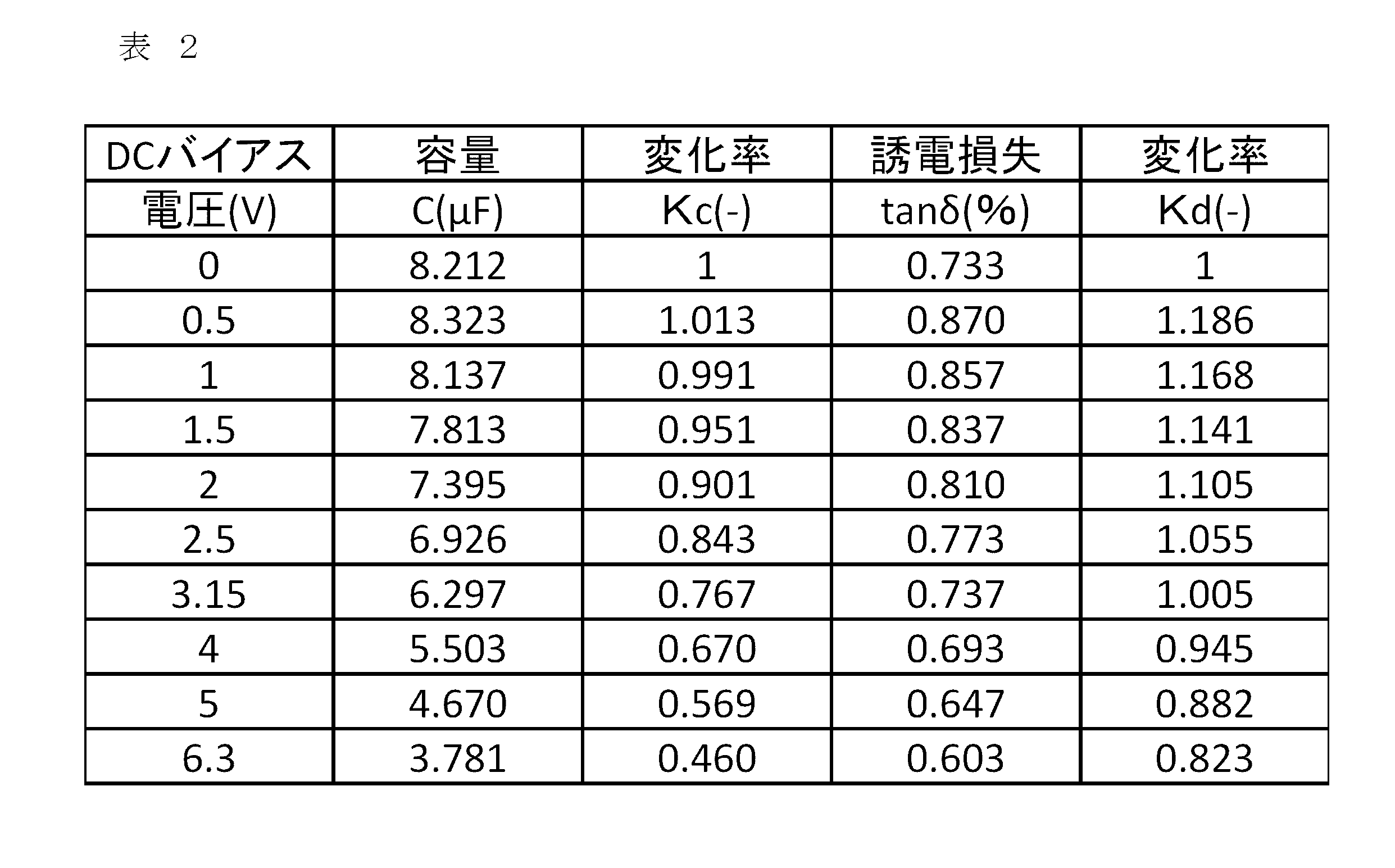
- Table 2 below shows the equivalent series capacitance C [ ⁇ F], dielectric loss tan ⁇ [%], and capacitance change rate Kc [ ⁇ ] and dielectric loss for these characteristic values when no DC voltage is applied.
- the change rate Kd [ ⁇ ] is shown.
- the capacitance change rate Kc and the dielectric loss change rate Kd are dimensionless quantities having no dimension, and [-] indicates that they are dimensionless.
- FIG. 13 (a) is a graph showing the capacitance change rate kc of the capacitor shown in Table 2 as an approximate function of the DC voltage Vdc applied to the capacitor.
- FIG. 5B is a graph showing the dielectric loss change rate Kd of the capacitor shown in Table 2 as an approximate function of the DC voltage Vdc applied to the capacitor.
- the horizontal axis represents the DC applied voltage (DC bias voltage) [V]
- the vertical axis represents the capacitance change rate Kc [ ⁇ ] and the dielectric loss change rate Kd [ ⁇ ].
- the approximate function of the capacitance change rate Kc is represented by the characteristic line H1
- the approximate function of the dielectric loss change rate Kd is represented by the characteristic line H2.
- a square mark plot p is a measured value of the capacitance change rate Kc and the dielectric loss change rate Kd shown in Table 2.
- Characteristic lines H1 and H2 connecting the plots p are derived based on the measured values, and in the present embodiment, represented by the exponential function exp (f (x)) as described above, and include odd-order power terms. Expressed with no polynomial form even function.
- the capacity change rate Kc and the dielectric loss change rate Kd as approximate functions in this way, the capacity change for any continuous DC voltage Vdc between the measured values discretely measured as shown in Table 2
- the rate Kc and the dielectric loss change rate Kd can be complemented, and a dimensionless coefficient for any continuous DC voltage Vdc can be obtained. Therefore, the characteristic change rates k R1 (Vdc) and k C1 (Vdc) are calculated by multiplying the dimensionless coefficient thus determined by the characteristic values of the resistance element R and the capacitance element C as described above.
- FIG. 14A is a passive equivalent circuit model when no DC voltage is applied to the capacitor in the fourth embodiment, based on the equivalent circuit model shown in FIG. 10, and FIG. 14B is an equivalent circuit model shown in FIG. It is a circuit diagram which shows the nonlinear equivalent circuit model of the capacitor
- the same or corresponding parts as those in FIGS. 4 and 10 are denoted by the same reference numerals, and the description thereof is omitted.
- the control current source B X shown in FIG. 10 is excluded. Further, in the nonlinear equivalent circuit model shown in FIG. 14B, voltage source models V RX , V CX , and V LX that measure the current flowing through the resistance element R X , the capacitance element C X , and the induction element L X are provided as ammeters. It has been. Also in each equivalent circuit model in the fourth embodiment, similarly to each equivalent circuit model in the second embodiment shown in FIG. 4, the control current source B X and the passive circuit elements R X , C X , L X A plurality of parallel circuits are connected in series. Further, similarly to the equivalent circuit model in the third embodiment shown in FIG. 9, the passive circuit elements r X , c X and l X whose characteristics are not changed by application of the DC voltage Vdc to the capacitor are configured. Yes.
- the passive equivalent circuit model shown in FIG. 14 (a) the AC voltage Vac to DC voltage Vdc is not applied is applied as a voltage V to the circuit by a voltage source model V 0 .
- the AC voltage Vac to DC voltage Vdc is applied, it is applied to the circuit by a voltage source model V 1 as the voltage V.
- the approximation function exp (f (x)) representing the characteristic line H1 shown in FIG.
- the characteristic change rates k RX (Vdc), k CX (Vdc), and k LX (Vdc) of the circuit elements R X , C X , and L X are calculated.
- the control current source B X performs the first implementation based on the calculated characteristic change rates k RX (Vdc), k CX (Vdc), k LX (Vdc) and the non-application currents I RX , I CX , I LX.
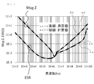
- FIG. 15A shows a calculated value calculated using the equivalent circuit model shown in FIG. 14 for the magnitude MagZ of the impedance Z of the capacitor when the DC voltage Vdc of 6.3 [V] of the rated voltage is applied. It is a graph which shows by comparing with a measured value. The horizontal axis of the graph represents the frequency [Hz], and the vertical axis represents the value [ ⁇ ] of the magnitude MagZ.
- a measured value of magnitude MagZ with a DC applied voltage Vd of 0 [V] is indicated by a solid characteristic line E0
- a measured value with a DC applied voltage Vdc of 6.3 [V] is indicated by a solid characteristic line E1.
- the calculated value of the magnitude MagZ and the DC applied voltage Vdc of 6.3 [V] is indicated by a broken characteristic line E2.
- FIG. 15B shows the calculated value calculated using the equivalent circuit model shown in FIG. 14 for the equivalent series resistance ESR of the capacitor when a DC voltage Vdc of 6.3 [V] is applied. It is a graph shown in comparison. The horizontal axis of the graph represents the frequency [Hz], and the vertical axis represents the value [ ⁇ ] of the equivalent series resistance ESR.
- the measured value of the equivalent series resistance ESR when the DC applied voltage Vdc is 0 [V] is indicated by a solid characteristic line F0
- the measured value when the DC applied voltage Vdc is 6.3 [V] is indicated by a solid characteristic line F1.
- the calculated value of the equivalent series resistance ESR when the DC applied voltage Vdc is 6.3 [V] is indicated by a broken characteristic line F2.
- the calculated values of the magnitude Z of the impedance Z and the equivalent series resistance ESR when each DC voltage Vdc is applied are 100 [Hz] to 8.5 [GHz]. Good agreement with each measurement over the entire band.
- each equivalent circuit model is applied to LTspice provided by Linear Technology Corporation.
- the circuit simulator to be applied is not limited to this.
- the present invention can be similarly applied to other circuit circuit simulators such as MicrowaIe Office provided by Applied Wae Research (AWR) and ADS provided by Agilent Technologies Inc. (Agilent).
- the capacitor simulation method and the capacitor nonlinear equivalent circuit model of each embodiment described above can be easily used by using the following computer program.
- the computer program includes a first step, a second step, and a third step.
- the first step the type of capacitor used for electronic circuit design is input.
- the second step the voltage V applied to the capacitor or the current I flowing to the capacitor is input.
- the third step the voltage V applied to the capacitor is measured by the voltage V or current I input in the second step, and the reference voltage Vref is referred to.
- the computer program implements the capacitor simulation method of each of the above-described embodiments or causes the non-linear equivalent circuit model of the capacitor of each of the above-described embodiments to function by arithmetic processing that executes these steps.
- the type of capacitor to be simulated and the voltage V applied to the capacitor or the value of the current I flowing to the capacitor are input to the computer program, so that the nonlinear characteristics of the input type of capacitor are:
- the computer program causes the differential currents ⁇ I RX (Vref), ⁇ I CX (Vref), ⁇ I LX (Vref) to flow in parallel to the no-application currents I RX , I CX , I LX of the passive circuit elements Rx, Cx, Lx. Simulated automatically.
- the user of this simulation method or this nonlinear equivalent circuit model can input the value of the type of capacitor to be simulated and the voltage V applied to the capacitor or the current I to be passed through the capacitor to the computer program.
- Circuit simulation can be performed with high accuracy and ease. As a result, even a general user who does not have specialized knowledge about circuit simulation can accurately and easily perform an accurate circuit simulation of an electronic circuit using a capacitor.
- the computer program can be used from a terminal such as a personal computer connected to the Internet network by accessing a server such as an electronic component manufacturer having the computer program via the Internet network. According to this configuration, the user can easily use the computer program by accessing a server including the computer program from a terminal connected to the Internet network. Therefore, it is possible to provide a large number of users with the capacitor simulation method and the capacitor nonlinear equivalent circuit model according to each of the above embodiments.
- Rx, Lx, Cx, r, l, c passive circuit elements
- B X ... controlled current source (behavioral source model) V nX , V RX , V CX ... Voltage source model (ammeter) V 0 , V 1 ... Voltage source model R X1 (Vdc) ... Variable resistance element C X1 (Vdc) ... Variable induction element
Landscapes
- Engineering & Computer Science (AREA)
- Computer Hardware Design (AREA)
- Physics & Mathematics (AREA)
- Theoretical Computer Science (AREA)
- General Physics & Mathematics (AREA)
- General Engineering & Computer Science (AREA)
- Mathematical Physics (AREA)
- Data Mining & Analysis (AREA)
- Microelectronics & Electronic Packaging (AREA)
- Evolutionary Computation (AREA)
- Geometry (AREA)
- Pure & Applied Mathematics (AREA)
- Databases & Information Systems (AREA)
- Software Systems (AREA)
- Mathematical Optimization (AREA)
- Mathematical Analysis (AREA)
- Computational Mathematics (AREA)
- Algebra (AREA)
- Semiconductor Integrated Circuits (AREA)
- Filters And Equalizers (AREA)
- Networks Using Active Elements (AREA)
Abstract
Description
v=vac+Vdc …(1)
C=C(Vdc)
=C0+C1Vdc+C2Vdc 2+C3Vdc 3+C4Vdc 4+C5Vdc 5+C6Vdc 6+…
…(2)
i=C(Vdc)・dv/dt …(3)
コンデンサの等価回路を受動回路素子を使って表し、
直流電圧印加時における受動回路素子の特性変化率を実測値を基に電圧を変数とする近似関数として表し、
コンデンサにかかる電圧を参照し、参照した電圧に対応して近似関数により算出される特性変化率、および直流電圧無印加時に受動回路素子に流れる無印加時電流に基づいて、直流電圧の印加によって特性が変化する受動回路素子に並列に接続される制御電流源により、直流電圧印加時に受動回路素子に流れる印加時電流と無印加時電流との差分電流を発生させ、無印加時電流に差分電流を併流させることで、
コンデンサの直流電圧印加時の非線形特性をシミュレートするコンデンサのシミュレーション方法を構成した。
コンデンサにかかる電圧を参照する電圧参照手段と、
直流電圧印加時における受動回路素子の特性変化率を実測値を基に電圧を変数として表す近似関数により、電圧参照手段によって参照される電圧に対応して算出される特性変化率、および直流電圧無印加時に受動回路素子に流れる無印加時電流に基づいて、直流電圧印加時に受動回路素子に流れる印加時電流と無印加時電流との差分電流を発生させる、直流電圧の印加によって特性が変化する受動回路素子に並列に接続される制御電流源と
を備えて、コンデンサの非線形等価回路モデルを構成した。
ΔI=I0×[exp(f(x))-1]
の関数形で与えられることを特徴とする。
コンデンサの種類を入力する第1のステップと、
コンデンサへ印加する電圧またはコンデンサへ流す電流を入力する第2のステップと、
第2のステップで入力された電圧または電流によってコンデンサにかかる電圧を参照し、第1のステップで入力された種類のコンデンサについて予め用意された近似関数により参照電圧に対応して算出される特性変化率、および無印加時電流に基づいて、制御電流源によって差分電流を発生させ、無印加時電流に差分電流を併流させることで、コンデンサの直流電圧印加時の非線形特性をシミュレートする第3のステップとを備え、
上記のいずれかのコンデンサのシミュレーション方法を実施する、または上記のいずれかのコンデンサの非線形等価回路モデルを機能させるコンピュータプログラムを構成した。
V=V1+V2 …(4)
I=V1/R2+CX1(Vdc)・dV1/dt …(5)
I=V2/RX1(Vdc) …(6)
I=V1/R2+C1・dV1/dt+ΔIC1(Vdc) …(7)
I=V2/R1+ΔIR1(Vdc) …(8)
ΔIC1(Vdc)
=IC1(Vdc)-IC1
=(CX1(Vdc)-C1)・dV1/dt
=(kC1(Vdc)-1)・C1・dV1/dt
=(kC1(Vdc)-1)・IC1 …(9)
kC1(Vdc)=CX1(Vdc)/C1 …(10)
ΔIR1(Vdc)
=IR1(Vdc)-IR1
=(1/RX1(Vdc)-1/R1)・V2
=(1/kR1(Vdc)-1)・V2/R1
=(1/kR1(Vdc)-1)・IR1 …(11)
kR1(Vdc)=RX1(Vdc)/R1 …(12)
ΔIC1(Vdc)=[exp(f(x))-1]・IC1 …(13)
ΔIR1(Vdc)=[exp(f(x))-1]・IR1 …(14)


BX…制御電流源(ビヘイビア電流源モデル)
VnX,VRX,VCX…電圧源モデル(電流計)
V0,V1…電圧源モデル
RX1(Vdc)…可変抵抗素子
CX1(Vdc)…可変誘導素子
Claims (11)
- コンデンサの等価回路を受動回路素子を使って表し、
直流電圧印加時における前記受動回路素子の特性変化率を実測値を基に電圧を変数とする近似関数として表し、
前記コンデンサにかかる電圧を参照し、参照した電圧に対応して前記近似関数により算出される前記特性変化率、および直流電圧無印加時に前記受動回路素子に流れる無印加時電流に基づいて、直流電圧の印加によって特性が変化する前記受動回路素子に並列に接続される制御電流源により、直流電圧印加時に前記受動回路素子に流れる印加時電流と前記無印加時電流との差分電流を発生させ、前記無印加時電流に前記差分電流を併流させることで、
コンデンサの直流電圧印加時の非線形特性をシミュレートするコンデンサのシミュレーション方法。 - コンデンサの等価回路を表す受動回路素子と、
前記コンデンサにかかる電圧を参照する電圧参照手段と、
直流電圧印加時における前記受動回路素子の特性変化率を実測値を基に電圧を変数として表す近似関数により、前記電圧参照手段によって参照される電圧に対応して算出される前記特性変化率、および直流電圧無印加時に前記受動回路素子に流れる無印加時電流に基づいて、直流電圧印加時に前記受動回路素子に流れる印加時電流と前記無印加時電流との差分電流を発生させる、直流電圧の印加によって特性が変化する前記受動回路素子に並列に接続される制御電流源と
を備えて構成されるコンデンサの非線形等価回路モデル。 - 前記差分電流は、前記差分電流をΔI、前記無印加時電流をI0、前記近似関数を参照する電圧xを変数とする関数exp(f(x))とした場合に、次式
ΔI=I0×[exp(f(x))-1]
の関数形で与えられる
ことを特徴とする請求項1に記載のコンデンサのシミュレーション方法または請求項2に記載のコンデンサの非線形等価回路モデル。 - 前記近似関数は奇数次のべき乗項を含まない多項式形式の偶関数で与えられることを特徴とする請求項1または請求項3に記載のコンデンサのシミュレーション方法または請求項2または請求項3に記載のコンデンサの非線形等価回路モデル。
- 前記コンデンサにかかる電圧は前記等価回路の両端で参照され、前記無印加時電流は前記受動回路素子の入力端または出力端で参照されることを特徴とする請求項1または請求項3または請求項4に記載のコンデンサのシミュレーション方法または請求項2から請求項4のいずれか1項に記載のコンデンサの非線形等価回路モデル。
- 前記制御電流源に並列に接続される前記受動回路素子は、容量素子単体、または容量素子と抵抗素子との並列回路、または容量素子と抵抗素子と誘導素子との並列回路であることを特徴とする請求項1または請求項3から請求項5のいずれか1項に記載のコンデンサのシミュレーション方法または請求項2から請求項5のいずれか1項に記載のコンデンサの非線形等価回路モデル。
- 前記制御電流源と前記受動回路素子との並列回路が複数直列に接続されることを特徴とする請求項1または請求項3から請求項6のいずれか1項に記載のコンデンサのシミュレーション方法または請求項2から請求項6のいずれか1項に記載のコンデンサの非線形等価回路モデル。
- 前記等価回路は、直流電圧の印加によって特性が変化しない前記受動回路素子を含んで構成されることを特徴とする請求項1または請求項3から請求項7のいずれか1項に記載のコンデンサのシミュレーション方法または請求項2から請求項7のいずれか1項に記載のコンデンサの非線形等価回路モデル。
- 請求項2から請求項8のいずれか1項に記載のコンデンサの非線形等価回路モデルを用いてコンデンサの直流電圧印加時の非線形特性をシミュレートするコンデンサのシミュレーション方法。
- 前記コンデンサの種類を入力する第1のステップと、
前記コンデンサへ印加する電圧または前記コンデンサへ流す電流を入力する第2のステップと、
前記第2のステップで入力された電圧または電流によって前記コンデンサにかかる電圧を参照し、前記第1のステップで入力された種類の前記コンデンサについて予め用意された前記近似関数により参照電圧に対応して算出される前記特性変化率、および前記無印加時電流に基づいて、前記制御電流源によって前記差分電流を発生させ、前記無印加時電流に前記差分電流を併流させることで、前記コンデンサの直流電圧印加時の非線形特性をシミュレートする第3のステップとを備え、
請求項1または請求項3から請求項9のいずれか1項に記載のコンデンサのシミュレーション方法を実施する、または請求項2から請求項8のいずれか1項に記載のコンデンサの非線形等価回路モデルを機能させるコンピュータプログラム。 - 前記コンピュータプログラムを備えるサーバにインターネット網を介してアクセスし、インターネット網に接続された端末から前記コンピュータプログラムを使用する請求項10に記載のコンピュータプログラムの使用方法。
Priority Applications (4)
| Application Number | Priority Date | Filing Date | Title |
|---|---|---|---|
| JP2015506028A JP5773101B2 (ja) | 2013-05-14 | 2014-05-02 | コンデンサのシミュレーション方法並びにコンデンサのシミュレーション装置およびその使用方法 |
| CN201480027885.2A CN105229644B (zh) | 2013-05-14 | 2014-05-02 | 电容器的仿真方法及电容器的非线性等效电路模型 |
| KR1020157032477A KR101616037B1 (ko) | 2013-05-14 | 2014-05-02 | 콘덴서의 시뮬레이션 방법 및 콘덴서의 비선형 등가 회로 모델 |
| US14/934,902 US10650180B2 (en) | 2013-05-14 | 2015-11-06 | Capacitor simulation method and capacitor nonlinear equivalent circuit model |
Applications Claiming Priority (2)
| Application Number | Priority Date | Filing Date | Title |
|---|---|---|---|
| JP2013102541 | 2013-05-14 | ||
| JP2013-102541 | 2013-05-14 |
Related Child Applications (1)
| Application Number | Title | Priority Date | Filing Date |
|---|---|---|---|
| US14/934,902 Continuation US10650180B2 (en) | 2013-05-14 | 2015-11-06 | Capacitor simulation method and capacitor nonlinear equivalent circuit model |
Publications (1)
| Publication Number | Publication Date |
|---|---|
| WO2014185293A1 true WO2014185293A1 (ja) | 2014-11-20 |
Family
ID=51898272
Family Applications (1)
| Application Number | Title | Priority Date | Filing Date |
|---|---|---|---|
| PCT/JP2014/062156 Ceased WO2014185293A1 (ja) | 2013-05-14 | 2014-05-02 | コンデンサのシミュレーション方法およびコンデンサの非線形等価回路モデル |
Country Status (5)
| Country | Link |
|---|---|
| US (1) | US10650180B2 (ja) |
| JP (1) | JP5773101B2 (ja) |
| KR (1) | KR101616037B1 (ja) |
| CN (1) | CN105229644B (ja) |
| WO (1) | WO2014185293A1 (ja) |
Cited By (3)
| Publication number | Priority date | Publication date | Assignee | Title |
|---|---|---|---|---|
| JP2018060516A (ja) * | 2016-09-30 | 2018-04-12 | 太陽誘電株式会社 | コンデンサの等価回路の構築方法,シミュレーション方法及びその装置 |
| JP2018160132A (ja) * | 2017-03-23 | 2018-10-11 | 太陽誘電株式会社 | 等価回路の構築方法,シミュレーション方法及びその装置 |
| CN119442659A (zh) * | 2024-10-30 | 2025-02-14 | 广东电网有限责任公司 | 电流在导电介质中的属性预测方法、装置和处理器 |
Families Citing this family (8)
| Publication number | Priority date | Publication date | Assignee | Title |
|---|---|---|---|---|
| CN106909751A (zh) * | 2016-12-14 | 2017-06-30 | 成都海威华芯科技有限公司 | 一种应用于mmic设计的热电耦合模型建立方法 |
| CN106786587B (zh) * | 2017-02-14 | 2019-05-03 | 上海华虹宏力半导体制造有限公司 | 降低电阻性元件网络谐波的方法 |
| US10755015B2 (en) * | 2017-08-21 | 2020-08-25 | Semiconductor Components Industries, Llc | Agnostic model of semiconductor devices and related methods |
| KR102041686B1 (ko) * | 2017-12-06 | 2019-11-27 | 삼성전기주식회사 | 인덕터 등가 회로를 저장하는 저장 장치 및 인덕터 등가 회로를 제공하는 서버 |
| CN111027271A (zh) * | 2019-11-04 | 2020-04-17 | 华北电力大学 | 直流电网非线性组件的电磁暂态等效建模方法 |
| JP7276284B2 (ja) * | 2020-08-27 | 2023-05-18 | 株式会社村田製作所 | 積層コンデンサのシミュレーションモデルの生成方法、および、積層コンデンサのシミュレーション方法 |
| CN112949239B (zh) * | 2021-03-22 | 2023-07-21 | 梁文毅 | 一种基于层次化模型的非线性迭代仿真方法 |
| CN119853224B (zh) * | 2025-03-19 | 2025-06-10 | 江西铜业技术研究院有限公司 | 一种电容去离子装备的节能控制方法、系统及介质 |
Citations (2)
| Publication number | Priority date | Publication date | Assignee | Title |
|---|---|---|---|---|
| JP2006163606A (ja) * | 2004-12-03 | 2006-06-22 | Nec Toppan Circuit Solutions Inc | 回路設計支援方法、回路設計支援システム、装置及びプログラム |
| WO2012090602A1 (ja) * | 2010-12-29 | 2012-07-05 | 株式会社村田製作所 | 等価回路モデル,プログラム及び記録媒体 |
Family Cites Families (29)
| Publication number | Priority date | Publication date | Assignee | Title |
|---|---|---|---|---|
| KR910000368B1 (ko) * | 1984-09-12 | 1991-01-24 | 마쯔시다덴기산교 가부시기가이샤 | 비선형 신호처리장치 |
| JPH04183005A (ja) * | 1990-11-16 | 1992-06-30 | Sumitomo Electric Ind Ltd | 高周波発振回路 |
| JP3050309B2 (ja) * | 1998-06-17 | 2000-06-12 | 日本電気株式会社 | モデリング方法およびシミュレーション方法 |
| US6832182B1 (en) * | 1999-04-08 | 2004-12-14 | Transim Technology Corporation | Circuit simulator |
| JP4507421B2 (ja) | 2001-02-27 | 2010-07-21 | パナソニック株式会社 | 受動素子の等価回路モデル導出方法、シミュレータ、及び記憶媒体 |
| JP3558074B2 (ja) * | 2001-12-10 | 2004-08-25 | 株式会社村田製作所 | 測定誤差の補正方法、電子部品の良否判定方法および電子部品特性測定装置 |
| US20030182639A1 (en) * | 2002-03-25 | 2003-09-25 | International Business Machines Corporation | Circuit simulator system and method |
| US20030188267A1 (en) * | 2002-03-29 | 2003-10-02 | International Business Machines Corporation | Circuit and method for modeling I/O |
| US7263477B2 (en) * | 2003-06-09 | 2007-08-28 | Cadence Design Systems, Inc. | Method and apparatus for modeling devices having different geometries |
| TWI276811B (en) * | 2004-05-26 | 2007-03-21 | Sanyo Electric Co | Recording medium with equivalent circuit model of storage element stored, recording medium for deriving program, deriving device, recording medium for simulation program, simulation device, design method, and method and device for deciding quality |
| US7383140B2 (en) * | 2004-08-16 | 2008-06-03 | National Instruments Corporation | Capacitance, inductance and impedance measurements using multi-tone stimulation and DSP algorithms |
| US20060217948A1 (en) * | 2005-03-23 | 2006-09-28 | Tdk Corporation | Component for a simulation tool |
| JP4378371B2 (ja) * | 2006-09-29 | 2009-12-02 | Tdk株式会社 | 積層コンデンサ |
| JP4010515B1 (ja) | 2007-03-26 | 2007-11-21 | 株式会社パワーシステム | キャパシタ等価回路の定数設定方法及び設定支援システム |
| JP2009099913A (ja) * | 2007-10-19 | 2009-05-07 | Nec Tokin Corp | 多端子型固体電解コンデンサ |
| US8120891B2 (en) * | 2007-12-17 | 2012-02-21 | Murata Manufacturing Co., Ltd. | Multilayer capacitor having low equivalent series inductance and controlled equivalent series resistance |
| CN102150165B (zh) * | 2008-09-30 | 2013-07-17 | 日立金属株式会社 | 电感元件的直流叠加特性的分析方法及电磁场模拟装置 |
| JP5121757B2 (ja) | 2009-03-02 | 2013-01-16 | 太陽誘電株式会社 | 積層チップインダクタの等価回路モデルの回路定数解析方法及び回路シミュレーション方法 |
| EP2491612B1 (en) * | 2009-10-19 | 2017-08-02 | Nuvera Fuel Cells, LLC | Battery state-of-charge management method |
| JP5475563B2 (ja) * | 2010-06-15 | 2014-04-16 | 太陽誘電株式会社 | 積層チップコンデンサの回路定数解析プログラム及び回路定数解析装置 |
| US8710810B1 (en) * | 2010-06-23 | 2014-04-29 | Volterra Semiconductor Corporation | Systems and methods for DC-to-DC converter control |
| JP2012150579A (ja) | 2011-01-17 | 2012-08-09 | Taiyo Yuden Co Ltd | コンデンサの回路シミュレーションモデル及びその構築方法,回路シミュレーション方法及び回路シミュレータ |
| US8886507B2 (en) * | 2011-07-13 | 2014-11-11 | General Electric Company | Methods and systems for simulating circuit operation |
| JP5573868B2 (ja) * | 2012-03-07 | 2014-08-20 | 株式会社村田製作所 | 等価回路作成方法、等価回路作成プログラム及び等価回路作成装置 |
| JP5861774B2 (ja) * | 2012-04-04 | 2016-02-16 | 株式会社村田製作所 | コンデンサの等価回路モデルの導出方法 |
| US8972913B1 (en) * | 2012-08-29 | 2015-03-03 | Invarian, Inc. | Concurrent multiparameter simulation system |
| US10664562B2 (en) * | 2013-02-24 | 2020-05-26 | Fairchild Semiconductor Corporation and University of Connecticut | Battery state of charge tracking, equivalent circuit selection and benchmarking |
| US20140375334A1 (en) * | 2013-06-21 | 2014-12-25 | Hamilton Sundstrand Corporation | Systems and methods for selecting circuit element values for a hybrid active power filter operating over a variable frequency |
| JP6148630B2 (ja) | 2014-02-13 | 2017-06-14 | ブリヂストンフローテック株式会社 | 加締装置 |
-
2014
- 2014-05-02 KR KR1020157032477A patent/KR101616037B1/ko active Active
- 2014-05-02 WO PCT/JP2014/062156 patent/WO2014185293A1/ja not_active Ceased
- 2014-05-02 CN CN201480027885.2A patent/CN105229644B/zh active Active
- 2014-05-02 JP JP2015506028A patent/JP5773101B2/ja active Active
-
2015
- 2015-11-06 US US14/934,902 patent/US10650180B2/en active Active
Patent Citations (2)
| Publication number | Priority date | Publication date | Assignee | Title |
|---|---|---|---|---|
| JP2006163606A (ja) * | 2004-12-03 | 2006-06-22 | Nec Toppan Circuit Solutions Inc | 回路設計支援方法、回路設計支援システム、装置及びプログラム |
| WO2012090602A1 (ja) * | 2010-12-29 | 2012-07-05 | 株式会社村田製作所 | 等価回路モデル,プログラム及び記録媒体 |
Non-Patent Citations (1)
| Title |
|---|
| TSUYOSHI HORIGOME: "Musho Tool de Model Sakusei & Tuning Nyumon Denshi Kairo Simulator LTspice de Jitsuhakei o Saigen! Dai 2 Kai Buhin: Denkai Condenser Oyo: Seiryu/Dengen Kairo", TRANSISTOR GIJUTSU, vol. 48, no. 8, 1 August 2011 (2011-08-01), pages 154 - 160 * |
Cited By (6)
| Publication number | Priority date | Publication date | Assignee | Title |
|---|---|---|---|---|
| JP2018060516A (ja) * | 2016-09-30 | 2018-04-12 | 太陽誘電株式会社 | コンデンサの等価回路の構築方法,シミュレーション方法及びその装置 |
| JP7063552B2 (ja) | 2016-09-30 | 2022-05-09 | 太陽誘電株式会社 | コンデンサの等価回路の構築方法,シミュレーション方法及びその装置 |
| JP2018160132A (ja) * | 2017-03-23 | 2018-10-11 | 太陽誘電株式会社 | 等価回路の構築方法,シミュレーション方法及びその装置 |
| JP7043178B2 (ja) | 2017-03-23 | 2022-03-29 | 太陽誘電株式会社 | 受動素子の等価回路のシミュレーション方法及びその装置 |
| CN119442659A (zh) * | 2024-10-30 | 2025-02-14 | 广东电网有限责任公司 | 电流在导电介质中的属性预测方法、装置和处理器 |
| CN119442659B (zh) * | 2024-10-30 | 2025-12-05 | 广东电网有限责任公司 | 电流在导电介质中的属性预测方法、装置和处理器 |
Also Published As
| Publication number | Publication date |
|---|---|
| CN105229644B (zh) | 2018-08-17 |
| KR101616037B1 (ko) | 2016-04-27 |
| US20160063159A1 (en) | 2016-03-03 |
| JP5773101B2 (ja) | 2015-09-02 |
| JPWO2014185293A1 (ja) | 2017-02-23 |
| CN105229644A (zh) | 2016-01-06 |
| US10650180B2 (en) | 2020-05-12 |
| KR20150133296A (ko) | 2015-11-27 |
Similar Documents
| Publication | Publication Date | Title |
|---|---|---|
| JP5773101B2 (ja) | コンデンサのシミュレーション方法並びにコンデンサのシミュレーション装置およびその使用方法 | |
| JP5773102B2 (ja) | インダクタのシミュレーション方法並びにインダクタのシミュレーション装置およびその使用方法 | |
| Elwy et al. | All possible topologies of the fractional-order Wien oscillator family using different approximation techniques | |
| US8718987B2 (en) | Circuit simulation model of capacitor, constructing method of simulation model, method of circuit simulation, circuit simulator | |
| US9563728B2 (en) | Equivalent circuit model, program, and recording medium | |
| Jakubowska et al. | Analysis of the transient state in a series circuit of the class RL β C α | |
| Myderrizi et al. | DXCCII-based grounded inductance simulators and filter applications | |
| EP2835749B1 (en) | Method for deriving capacitor equivalent circuit model | |
| Kapoulea et al. | Realizations of simple fractional-order capacitor emulators with electronically-tunable capacitance | |
| WO2017000585A1 (zh) | 一种电路仿真方法和装置 | |
| CN107706908B (zh) | 一种基于端口阻抗零极点匹配的电力系统交流网络分频段等值方法 | |
| US20180096088A1 (en) | Method of constructing and method of simulating equivalent circuit for capacitor, and simulation device therefor | |
| Cao et al. | Parametric modeling of microwave passive components using combined neural networks and transfer functions in the time and frequency | |
| JP7063552B2 (ja) | コンデンサの等価回路の構築方法,シミュレーション方法及びその装置 | |
| US20140074449A1 (en) | Scalable power model calibration | |
| Satish et al. | Determination and comparison of temperature coefficient of standard inductors by measuring change in inductance and resistances | |
| Elwakil et al. | Indirect realization of the imaginary resistor jR | |
| Sandoval-Ibarra et al. | Design of 2nd order low-pass active filters by preserving the physical meaning of design variables | |
| WO2015015910A1 (ja) | 印加交流電圧を考慮したコンデンサの静電容量値決定方法およびプログラム | |
| Tarunkumar et al. | Operational Amplifier-Based Fractional Device of Order s±0.5 | |
| Liang et al. | Rational modeling of on-chip inductor by vector fitting | |
| CN105929239B (zh) | 一种非正弦交流电路中无源元件参数的定量检测和定性识别方法 | |
| Tschoban et al. | Comparison of methods for impedance modeling of power distribution networks |
Legal Events
| Date | Code | Title | Description |
|---|---|---|---|
| WWE | Wipo information: entry into national phase |
Ref document number: 201480027885.2 Country of ref document: CN |
|
| 121 | Ep: the epo has been informed by wipo that ep was designated in this application |
Ref document number: 14798143 Country of ref document: EP Kind code of ref document: A1 |
|
| ENP | Entry into the national phase |
Ref document number: 2015506028 Country of ref document: JP Kind code of ref document: A |
|
| ENP | Entry into the national phase |
Ref document number: 20157032477 Country of ref document: KR Kind code of ref document: A |
|
| NENP | Non-entry into the national phase |
Ref country code: DE |
|
| 122 | Ep: pct application non-entry in european phase |
Ref document number: 14798143 Country of ref document: EP Kind code of ref document: A1 |