WO2014178284A1 - 熱電変換材料、熱電変換素子、熱電発電用物品及びセンサー用電源 - Google Patents
熱電変換材料、熱電変換素子、熱電発電用物品及びセンサー用電源 Download PDFInfo
- Publication number
- WO2014178284A1 WO2014178284A1 PCT/JP2014/060844 JP2014060844W WO2014178284A1 WO 2014178284 A1 WO2014178284 A1 WO 2014178284A1 JP 2014060844 W JP2014060844 W JP 2014060844W WO 2014178284 A1 WO2014178284 A1 WO 2014178284A1
- Authority
- WO
- WIPO (PCT)
- Prior art keywords
- thermoelectric conversion
- group
- general formula
- conversion element
- integer
- Prior art date
- Legal status (The legal status is an assumption and is not a legal conclusion. Google has not performed a legal analysis and makes no representation as to the accuracy of the status listed.)
- Ceased
Links
Images


Classifications
-
- C—CHEMISTRY; METALLURGY
- C07—ORGANIC CHEMISTRY
- C07C—ACYCLIC OR CARBOCYCLIC COMPOUNDS
- C07C381/00—Compounds containing carbon and sulfur and having functional groups not covered by groups C07C301/00 - C07C337/00
- C07C381/12—Sulfonium compounds
-
- C—CHEMISTRY; METALLURGY
- C07—ORGANIC CHEMISTRY
- C07D—HETEROCYCLIC COMPOUNDS
- C07D213/00—Heterocyclic compounds containing six-membered rings, not condensed with other rings, with one nitrogen atom as the only ring hetero atom and three or more double bonds between ring members or between ring members and non-ring members
- C07D213/02—Heterocyclic compounds containing six-membered rings, not condensed with other rings, with one nitrogen atom as the only ring hetero atom and three or more double bonds between ring members or between ring members and non-ring members having three double bonds between ring members or between ring members and non-ring members
- C07D213/04—Heterocyclic compounds containing six-membered rings, not condensed with other rings, with one nitrogen atom as the only ring hetero atom and three or more double bonds between ring members or between ring members and non-ring members having three double bonds between ring members or between ring members and non-ring members having no bond between the ring nitrogen atom and a non-ring member or having only hydrogen or carbon atoms directly attached to the ring nitrogen atom
-
- C—CHEMISTRY; METALLURGY
- C07—ORGANIC CHEMISTRY
- C07D—HETEROCYCLIC COMPOUNDS
- C07D213/00—Heterocyclic compounds containing six-membered rings, not condensed with other rings, with one nitrogen atom as the only ring hetero atom and three or more double bonds between ring members or between ring members and non-ring members
- C07D213/02—Heterocyclic compounds containing six-membered rings, not condensed with other rings, with one nitrogen atom as the only ring hetero atom and three or more double bonds between ring members or between ring members and non-ring members having three double bonds between ring members or between ring members and non-ring members
- C07D213/04—Heterocyclic compounds containing six-membered rings, not condensed with other rings, with one nitrogen atom as the only ring hetero atom and three or more double bonds between ring members or between ring members and non-ring members having three double bonds between ring members or between ring members and non-ring members having no bond between the ring nitrogen atom and a non-ring member or having only hydrogen or carbon atoms directly attached to the ring nitrogen atom
- C07D213/06—Heterocyclic compounds containing six-membered rings, not condensed with other rings, with one nitrogen atom as the only ring hetero atom and three or more double bonds between ring members or between ring members and non-ring members having three double bonds between ring members or between ring members and non-ring members having no bond between the ring nitrogen atom and a non-ring member or having only hydrogen or carbon atoms directly attached to the ring nitrogen atom containing only hydrogen and carbon atoms in addition to the ring nitrogen atom
- C07D213/16—Heterocyclic compounds containing six-membered rings, not condensed with other rings, with one nitrogen atom as the only ring hetero atom and three or more double bonds between ring members or between ring members and non-ring members having three double bonds between ring members or between ring members and non-ring members having no bond between the ring nitrogen atom and a non-ring member or having only hydrogen or carbon atoms directly attached to the ring nitrogen atom containing only hydrogen and carbon atoms in addition to the ring nitrogen atom containing only one pyridine ring
- C07D213/20—Quaternary compounds thereof
-
- C—CHEMISTRY; METALLURGY
- C07—ORGANIC CHEMISTRY
- C07D—HETEROCYCLIC COMPOUNDS
- C07D213/00—Heterocyclic compounds containing six-membered rings, not condensed with other rings, with one nitrogen atom as the only ring hetero atom and three or more double bonds between ring members or between ring members and non-ring members
- C07D213/02—Heterocyclic compounds containing six-membered rings, not condensed with other rings, with one nitrogen atom as the only ring hetero atom and three or more double bonds between ring members or between ring members and non-ring members having three double bonds between ring members or between ring members and non-ring members
- C07D213/04—Heterocyclic compounds containing six-membered rings, not condensed with other rings, with one nitrogen atom as the only ring hetero atom and three or more double bonds between ring members or between ring members and non-ring members having three double bonds between ring members or between ring members and non-ring members having no bond between the ring nitrogen atom and a non-ring member or having only hydrogen or carbon atoms directly attached to the ring nitrogen atom
- C07D213/06—Heterocyclic compounds containing six-membered rings, not condensed with other rings, with one nitrogen atom as the only ring hetero atom and three or more double bonds between ring members or between ring members and non-ring members having three double bonds between ring members or between ring members and non-ring members having no bond between the ring nitrogen atom and a non-ring member or having only hydrogen or carbon atoms directly attached to the ring nitrogen atom containing only hydrogen and carbon atoms in addition to the ring nitrogen atom
- C07D213/22—Heterocyclic compounds containing six-membered rings, not condensed with other rings, with one nitrogen atom as the only ring hetero atom and three or more double bonds between ring members or between ring members and non-ring members having three double bonds between ring members or between ring members and non-ring members having no bond between the ring nitrogen atom and a non-ring member or having only hydrogen or carbon atoms directly attached to the ring nitrogen atom containing only hydrogen and carbon atoms in addition to the ring nitrogen atom containing two or more pyridine rings directly linked together, e.g. bipyridyl
-
- C—CHEMISTRY; METALLURGY
- C07—ORGANIC CHEMISTRY
- C07D—HETEROCYCLIC COMPOUNDS
- C07D213/00—Heterocyclic compounds containing six-membered rings, not condensed with other rings, with one nitrogen atom as the only ring hetero atom and three or more double bonds between ring members or between ring members and non-ring members
- C07D213/02—Heterocyclic compounds containing six-membered rings, not condensed with other rings, with one nitrogen atom as the only ring hetero atom and three or more double bonds between ring members or between ring members and non-ring members having three double bonds between ring members or between ring members and non-ring members
- C07D213/04—Heterocyclic compounds containing six-membered rings, not condensed with other rings, with one nitrogen atom as the only ring hetero atom and three or more double bonds between ring members or between ring members and non-ring members having three double bonds between ring members or between ring members and non-ring members having no bond between the ring nitrogen atom and a non-ring member or having only hydrogen or carbon atoms directly attached to the ring nitrogen atom
- C07D213/60—Heterocyclic compounds containing six-membered rings, not condensed with other rings, with one nitrogen atom as the only ring hetero atom and three or more double bonds between ring members or between ring members and non-ring members having three double bonds between ring members or between ring members and non-ring members having no bond between the ring nitrogen atom and a non-ring member or having only hydrogen or carbon atoms directly attached to the ring nitrogen atom with hetero atoms or with carbon atoms having three bonds to hetero atoms with at the most one bond to halogen, e.g. ester or nitrile radicals, directly attached to ring carbon atoms
- C07D213/62—Oxygen or sulfur atoms
- C07D213/63—One oxygen atom
- C07D213/68—One oxygen atom attached in position 4
-
- C—CHEMISTRY; METALLURGY
- C07—ORGANIC CHEMISTRY
- C07D—HETEROCYCLIC COMPOUNDS
- C07D213/00—Heterocyclic compounds containing six-membered rings, not condensed with other rings, with one nitrogen atom as the only ring hetero atom and three or more double bonds between ring members or between ring members and non-ring members
- C07D213/02—Heterocyclic compounds containing six-membered rings, not condensed with other rings, with one nitrogen atom as the only ring hetero atom and three or more double bonds between ring members or between ring members and non-ring members having three double bonds between ring members or between ring members and non-ring members
- C07D213/04—Heterocyclic compounds containing six-membered rings, not condensed with other rings, with one nitrogen atom as the only ring hetero atom and three or more double bonds between ring members or between ring members and non-ring members having three double bonds between ring members or between ring members and non-ring members having no bond between the ring nitrogen atom and a non-ring member or having only hydrogen or carbon atoms directly attached to the ring nitrogen atom
- C07D213/60—Heterocyclic compounds containing six-membered rings, not condensed with other rings, with one nitrogen atom as the only ring hetero atom and three or more double bonds between ring members or between ring members and non-ring members having three double bonds between ring members or between ring members and non-ring members having no bond between the ring nitrogen atom and a non-ring member or having only hydrogen or carbon atoms directly attached to the ring nitrogen atom with hetero atoms or with carbon atoms having three bonds to hetero atoms with at the most one bond to halogen, e.g. ester or nitrile radicals, directly attached to ring carbon atoms
- C07D213/72—Nitrogen atoms
- C07D213/74—Amino or imino radicals substituted by hydrocarbon or substituted hydrocarbon radicals
-
- C—CHEMISTRY; METALLURGY
- C07—ORGANIC CHEMISTRY
- C07D—HETEROCYCLIC COMPOUNDS
- C07D215/00—Heterocyclic compounds containing quinoline or hydrogenated quinoline ring systems
- C07D215/02—Heterocyclic compounds containing quinoline or hydrogenated quinoline ring systems having no bond between the ring nitrogen atom and a non-ring member or having only hydrogen atoms or carbon atoms directly attached to the ring nitrogen atom
- C07D215/04—Heterocyclic compounds containing quinoline or hydrogenated quinoline ring systems having no bond between the ring nitrogen atom and a non-ring member or having only hydrogen atoms or carbon atoms directly attached to the ring nitrogen atom with only hydrogen atoms or radicals containing only hydrogen and carbon atoms, directly attached to the ring carbon atoms
- C07D215/10—Quaternary compounds
-
- C—CHEMISTRY; METALLURGY
- C07—ORGANIC CHEMISTRY
- C07D—HETEROCYCLIC COMPOUNDS
- C07D233/00—Heterocyclic compounds containing 1,3-diazole or hydrogenated 1,3-diazole rings, not condensed with other rings
- C07D233/54—Heterocyclic compounds containing 1,3-diazole or hydrogenated 1,3-diazole rings, not condensed with other rings having two double bonds between ring members or between ring members and non-ring members
- C07D233/56—Heterocyclic compounds containing 1,3-diazole or hydrogenated 1,3-diazole rings, not condensed with other rings having two double bonds between ring members or between ring members and non-ring members with only hydrogen atoms or radicals containing only hydrogen and carbon atoms, attached to ring carbon atoms
- C07D233/58—Heterocyclic compounds containing 1,3-diazole or hydrogenated 1,3-diazole rings, not condensed with other rings having two double bonds between ring members or between ring members and non-ring members with only hydrogen atoms or radicals containing only hydrogen and carbon atoms, attached to ring carbon atoms with only hydrogen atoms or radicals containing only hydrogen and carbon atoms, attached to ring nitrogen atoms
-
- C—CHEMISTRY; METALLURGY
- C07—ORGANIC CHEMISTRY
- C07D—HETEROCYCLIC COMPOUNDS
- C07D235/00—Heterocyclic compounds containing 1,3-diazole or hydrogenated 1,3-diazole rings, condensed with other rings
- C07D235/02—Heterocyclic compounds containing 1,3-diazole or hydrogenated 1,3-diazole rings, condensed with other rings condensed with carbocyclic rings or ring systems
- C07D235/04—Benzimidazoles; Hydrogenated benzimidazoles
- C07D235/06—Benzimidazoles; Hydrogenated benzimidazoles with only hydrogen atoms, hydrocarbon or substituted hydrocarbon radicals, directly attached in position 2
-
- C—CHEMISTRY; METALLURGY
- C07—ORGANIC CHEMISTRY
- C07D—HETEROCYCLIC COMPOUNDS
- C07D295/00—Heterocyclic compounds containing polymethylene-imine rings with at least five ring members, 3-azabicyclo [3.2.2] nonane, piperazine, morpholine or thiomorpholine rings, having only hydrogen atoms directly attached to the ring carbon atoms
- C07D295/02—Heterocyclic compounds containing polymethylene-imine rings with at least five ring members, 3-azabicyclo [3.2.2] nonane, piperazine, morpholine or thiomorpholine rings, having only hydrogen atoms directly attached to the ring carbon atoms containing only hydrogen and carbon atoms in addition to the ring hetero elements
- C07D295/037—Heterocyclic compounds containing polymethylene-imine rings with at least five ring members, 3-azabicyclo [3.2.2] nonane, piperazine, morpholine or thiomorpholine rings, having only hydrogen atoms directly attached to the ring carbon atoms containing only hydrogen and carbon atoms in addition to the ring hetero elements with quaternary ring nitrogen atoms
-
- C—CHEMISTRY; METALLURGY
- C07—ORGANIC CHEMISTRY
- C07D—HETEROCYCLIC COMPOUNDS
- C07D333/00—Heterocyclic compounds containing five-membered rings having one sulfur atom as the only ring hetero atom
- C07D333/02—Heterocyclic compounds containing five-membered rings having one sulfur atom as the only ring hetero atom not condensed with other rings
- C07D333/46—Heterocyclic compounds containing five-membered rings having one sulfur atom as the only ring hetero atom not condensed with other rings substituted on the ring sulfur atom
-
- C—CHEMISTRY; METALLURGY
- C07—ORGANIC CHEMISTRY
- C07D—HETEROCYCLIC COMPOUNDS
- C07D409/00—Heterocyclic compounds containing two or more hetero rings, at least one ring having sulfur atoms as the only ring hetero atoms
- C07D409/02—Heterocyclic compounds containing two or more hetero rings, at least one ring having sulfur atoms as the only ring hetero atoms containing two hetero rings
- C07D409/04—Heterocyclic compounds containing two or more hetero rings, at least one ring having sulfur atoms as the only ring hetero atoms containing two hetero rings directly linked by a ring-member-to-ring-member bond
-
- C—CHEMISTRY; METALLURGY
- C07—ORGANIC CHEMISTRY
- C07D—HETEROCYCLIC COMPOUNDS
- C07D409/00—Heterocyclic compounds containing two or more hetero rings, at least one ring having sulfur atoms as the only ring hetero atoms
- C07D409/02—Heterocyclic compounds containing two or more hetero rings, at least one ring having sulfur atoms as the only ring hetero atoms containing two hetero rings
- C07D409/06—Heterocyclic compounds containing two or more hetero rings, at least one ring having sulfur atoms as the only ring hetero atoms containing two hetero rings linked by a carbon chain containing only aliphatic carbon atoms
-
- C—CHEMISTRY; METALLURGY
- C07—ORGANIC CHEMISTRY
- C07D—HETEROCYCLIC COMPOUNDS
- C07D453/00—Heterocyclic compounds containing quinuclidine or iso-quinuclidine ring systems, e.g. quinine alkaloids
- C07D453/02—Heterocyclic compounds containing quinuclidine or iso-quinuclidine ring systems, e.g. quinine alkaloids containing not further condensed quinuclidine ring systems
-
- C—CHEMISTRY; METALLURGY
- C07—ORGANIC CHEMISTRY
- C07D—HETEROCYCLIC COMPOUNDS
- C07D487/00—Heterocyclic compounds containing nitrogen atoms as the only ring hetero atoms in the condensed system, not provided for by groups C07D451/00 - C07D477/00
- C07D487/02—Heterocyclic compounds containing nitrogen atoms as the only ring hetero atoms in the condensed system, not provided for by groups C07D451/00 - C07D477/00 in which the condensed system contains two hetero rings
- C07D487/08—Bridged systems
-
- C—CHEMISTRY; METALLURGY
- C07—ORGANIC CHEMISTRY
- C07F—ACYCLIC, CARBOCYCLIC OR HETEROCYCLIC COMPOUNDS CONTAINING ELEMENTS OTHER THAN CARBON, HYDROGEN, HALOGEN, OXYGEN, NITROGEN, SULFUR, SELENIUM OR TELLURIUM
- C07F9/00—Compounds containing elements of Groups 5 or 15 of the Periodic Table
- C07F9/02—Phosphorus compounds
- C07F9/28—Phosphorus compounds with one or more P—C bonds
- C07F9/54—Quaternary phosphonium compounds
- C07F9/5407—Acyclic saturated phosphonium compounds
-
- C—CHEMISTRY; METALLURGY
- C07—ORGANIC CHEMISTRY
- C07F—ACYCLIC, CARBOCYCLIC OR HETEROCYCLIC COMPOUNDS CONTAINING ELEMENTS OTHER THAN CARBON, HYDROGEN, HALOGEN, OXYGEN, NITROGEN, SULFUR, SELENIUM OR TELLURIUM
- C07F9/00—Compounds containing elements of Groups 5 or 15 of the Periodic Table
- C07F9/02—Phosphorus compounds
- C07F9/28—Phosphorus compounds with one or more P—C bonds
- C07F9/54—Quaternary phosphonium compounds
- C07F9/5442—Aromatic phosphonium compounds (P-C aromatic linkage)
-
- C—CHEMISTRY; METALLURGY
- C07—ORGANIC CHEMISTRY
- C07F—ACYCLIC, CARBOCYCLIC OR HETEROCYCLIC COMPOUNDS CONTAINING ELEMENTS OTHER THAN CARBON, HYDROGEN, HALOGEN, OXYGEN, NITROGEN, SULFUR, SELENIUM OR TELLURIUM
- C07F9/00—Compounds containing elements of Groups 5 or 15 of the Periodic Table
- C07F9/02—Phosphorus compounds
- C07F9/547—Heterocyclic compounds, e.g. containing phosphorus as a ring hetero atom
- C07F9/6564—Heterocyclic compounds, e.g. containing phosphorus as a ring hetero atom having phosphorus atoms, with or without nitrogen, oxygen, sulfur, selenium or tellurium atoms, as ring hetero atoms
- C07F9/6568—Heterocyclic compounds, e.g. containing phosphorus as a ring hetero atom having phosphorus atoms, with or without nitrogen, oxygen, sulfur, selenium or tellurium atoms, as ring hetero atoms having phosphorus atoms as the only ring hetero atoms
- C07F9/65688—Heterocyclic compounds, e.g. containing phosphorus as a ring hetero atom having phosphorus atoms, with or without nitrogen, oxygen, sulfur, selenium or tellurium atoms, as ring hetero atoms having phosphorus atoms as the only ring hetero atoms the ring phosphorus atom being part of a phosphonium compound
-
- H—ELECTRICITY
- H10—SEMICONDUCTOR DEVICES; ELECTRIC SOLID-STATE DEVICES NOT OTHERWISE PROVIDED FOR
- H10N—ELECTRIC SOLID-STATE DEVICES NOT OTHERWISE PROVIDED FOR
- H10N10/00—Thermoelectric devices comprising a junction of dissimilar materials, i.e. devices exhibiting Seebeck or Peltier effects
- H10N10/80—Constructional details
- H10N10/85—Thermoelectric active materials
- H10N10/856—Thermoelectric active materials comprising organic compositions
-
- H—ELECTRICITY
- H10—SEMICONDUCTOR DEVICES; ELECTRIC SOLID-STATE DEVICES NOT OTHERWISE PROVIDED FOR
- H10N—ELECTRIC SOLID-STATE DEVICES NOT OTHERWISE PROVIDED FOR
- H10N10/00—Thermoelectric devices comprising a junction of dissimilar materials, i.e. devices exhibiting Seebeck or Peltier effects
- H10N10/80—Constructional details
- H10N10/85—Thermoelectric active materials
- H10N10/857—Thermoelectric active materials comprising compositions changing continuously or discontinuously inside the material
Definitions
- the present invention relates to a thermoelectric conversion material, a thermoelectric conversion element, an article for thermoelectric power generation using these, and a power source for sensors.
- thermoelectric conversion materials that can mutually convert heat energy and electrical energy are used in thermoelectric conversion elements such as thermoelectric power generation elements and Peltier elements.
- thermoelectric power generation using thermoelectric conversion materials and thermoelectric conversion elements can directly convert thermal energy into electric power, does not require moving parts, and is used for wristwatches that operate at body temperature, power supplies for remote areas, power supplies for space, etc. ing.
- thermoelectric conversion performance is a dimensionless figure of merit ZT (hereinafter, simply referred to as a figure of merit ZT).
- This figure of merit ZT is represented by the following formula (A).
- thermoelectromotive force hereinafter sometimes referred to as thermoelectromotive force
- conductivity ⁇ per absolute temperature 1K Reduction of thermal conductivity ⁇ is important.
- thermoelectric conversion materials are required to have good thermoelectric conversion performance, and inorganic materials are mainly put into practical use at present.
- the inorganic material has a complicated processing process for the thermoelectric conversion element, is expensive, and may contain harmful substances.
- organic thermoelectric conversion elements can be manufactured at a relatively low cost and can be easily processed such as film formation, research has been actively conducted in recent years. Has been reported.
- an organic material having a high Seebeck coefficient and electrical conductivity and low thermal conductivity is required.
- a thermoelectric conversion material made of a conductive polymer has been proposed (see Patent Document 1).
- thermoelectric conversion layer As a conductive organic material, a nanoconductive material (a nanometer-sized conductive material) such as a carbon nanotube is known.
- nano-conductive materials tend to aggregate due to intermolecular forces and have very poor dispersibility. Therefore, when a thermoelectric conversion layer is formed using a thermoelectric conversion material containing a nano-conductive material, adhesion with a base material or an electrode is deteriorated, resulting in a decrease in thermoelectric conversion performance.
- the present invention has a good dispersibility of the nano-conductive material, a thermoelectric conversion material having a high thermoelectromotive force, and uses this for the thermoelectric conversion layer, and is excellent in adhesion between the thermoelectric conversion layer and the electrode and thermoelectric conversion performance. It is an object of the present invention to provide a thermoelectric conversion element, a thermoelectric power generation article using the thermoelectric conversion element, and a sensor power source.
- the present inventors have studied an organic material that can enhance the dispersibility of the nanoconductive material by coexisting with the nanoconductive material in the thermoelectric conversion layer of the thermoelectric conversion element. As a result, it was found that by using an ionic compound having a specific structure together with the nanoconductive material, the dispersibility of the nanoconductive material is improved and a thermoelectric conversion material having a high thermoelectromotive force can be obtained. .
- the thermoelectric conversion element using the material for the thermoelectric conversion layer is excellent in adhesion between the thermoelectric conversion layer and the electrode and exhibits high thermoelectric conversion performance.
- the present invention has been completed based on these findings.
- thermoelectric conversion element having a first electrode, a thermoelectric conversion layer, and a second electrode on a base material, wherein the thermoelectric conversion layer includes a nano-conductive material and the following general formulas (1a) to (3b):
- the thermoelectric conversion element containing the at least 1 sort (s) of compound selected from the compound represented by this.
- X ⁇ represents a counter anion.
- R 11 to R 13 each independently represents an alkyl group or a heteroaryl group.
- R 12 and R 13 may combine with each other to form a ring.
- n represents an integer of 2 or 3.
- X p- represents a p-valent counter anion, and p represents an integer of 1 to 3.
- k represents an integer of 1 to 3.
- L represents an n-valent linking group or a single bond.
- R ⁇ 12 > and R ⁇ 13 > are synonymous with General formula (1a).
- the plurality of R 12 and R 13 may be the same or different.
- X ⁇ represents a counter anion.
- R 21 to R 24 each independently represents an alkyl group, an aryl group, or a heteroaryl group. Any two groups selected from R 21 to R 24 may be bonded to each other to form a ring.
- n represents an integer of 2 or 3.
- X p- represents a p-valent counter anion, and p represents an integer of 1 to 3.
- k represents an integer of 1 to 3.
- n kp.
- L represents an n-valent linking group or a single bond.
- R 22 to R 24 have the same meaning as in general formula (2a). The plurality of R 22 to R 24 may be the same or different.
- X ⁇ represents a counter anion.
- A represents a nitrogen-containing heterocyclic group.
- R 31 and R 32 each independently represents an alkyl group, an aryl group, or a heteroaryl group. R 31 may combine with A to form a ring.
- m represents 0 or 1
- m is 0 when A is a nitrogen-containing aromatic heterocyclic group
- m is 1 when A is a nitrogen-containing aliphatic heterocyclic group.
- n represents an integer of 2 or 3.
- X p- represents a p-valent counter anion, and p represents an integer of 1 to 3.
- k represents an integer of 1 to 3.
- n kp.
- L represents an n-valent linking group or a single bond.
- A, R 32 and m have the same meanings as in the general formula (3a).
- a plurality of A and R 32 may be the same or different.
- thermoelectric conversion element according to ⁇ 1> wherein in the general formulas (1a) and (1b), R 11 to R 13 are alkyl groups.
- X ⁇ or X p ⁇ is a conjugate base of a strong acid.
- thermoelectric conversion element according to any one of ⁇ 1> to ⁇ 5>, wherein the compounds represented by the general formulas (1a) to (3b) have a melting point of 100 ° C. or lower.
- the content ratio of the nanoconductive material and the compounds represented by the general formulas (1a) to (3b) in the thermoelectric conversion layer is 1: 9 to 9: 1 on a mass basis, ⁇ 1> to ⁇ 1
- ⁇ 8> The thermoelectric conversion element according to any one of ⁇ 1> to ⁇ 7>, wherein the nano conductive material is a carbon nanotube.
- thermoelectric conversion according to any one of ⁇ 1> to ⁇ 8>, wherein the first electrode and the second electrode are each independently formed of aluminum, gold, silver, or copper. element.
- thermoelectric conversion element according to any one of ⁇ 1> to ⁇ 9>, wherein the thermoelectric conversion layer contains a conjugated polymer.
- thermoelectric conversion layer contains a conjugated polymer.
- thermoelectric conversion material for forming a thermoelectric conversion layer of a thermoelectric conversion element comprising a nano-conductive material and at least one compound selected from compounds of the following general formulas (1a) to (3b).
- thermoelectric conversion material according to ⁇ 13> which contains an organic solvent.
- thermoelectric conversion material according to ⁇ 14> wherein the nanoconductive material is dispersed in an organic solvent.
- a numerical range expressed using “to” means a range including numerical values described before and after “to” as a lower limit value and an upper limit value.
- the xxx group when the xxx group is referred to as a substituent, the xxx group may have an arbitrary substituent.
- the repeating structure represented by each formula includes different repeating structures as long as they are within the range represented by the formula, even if they are not exactly the same repeating structure.
- the repeating structure represented by each formula may be only a repeating structure having a methyl group, and has another alkyl group such as an ethyl group in addition to the repeating structure having a methyl group. It may contain a repeating structure.
- thermoelectric conversion material of the present invention has good dispersibility of the nano-conductive material and has a high thermoelectromotive force.
- the heat conversion element of the present invention using the material for the thermoelectric conversion layer is excellent in adhesion between the thermoelectric conversion layer and the electrode, and exhibits high thermoelectric conversion performance.
- thermoelectric power-generating article and sensor power source of the present invention using the thermoelectric conversion element exhibit excellent thermoelectric conversion performance.
- thermoelectric conversion element of this invention It is a figure which shows typically the cross section of an example of the thermoelectric conversion element of this invention.
- the arrows in FIG. 1 indicate the direction of the temperature difference applied when the element is used.
- FIG. 2 shows typically the cross section of another example of the thermoelectric conversion element of this invention.
- thermoelectric conversion element of the present invention has a first electrode, a thermoelectric conversion layer, and a second electrode on a base material.
- the thermoelectric conversion layer is formed on the substrate by the thermoelectric conversion material of the present invention containing a nano conductive material and at least one compound selected from the compounds represented by the following general formulas (1a) to (3b). Molded.
- thermoelectric conversion performance of the thermoelectric conversion element of the present invention can be expressed by a figure of merit ZT represented by the following formula (A).
- Figure of merit ZT S 2 ⁇ ⁇ ⁇ T / ⁇ (A)
- thermoelectric conversion element is used for a wristwatch, a power source for remote areas, a power source for space, and the like, it is also required that the initial thermoelectric conversion performance can be maintained over a long period of time.
- thermoelectric conversion element functions to transmit the temperature difference in the thickness direction or the surface direction in a state where the temperature difference is generated in the thickness direction or the surface direction of the thermoelectric conversion layer. Therefore, it is necessary to form the thermoelectric conversion layer by forming it into a shape having a thickness of 2 mm. For this reason, when the thermoelectric conversion layer is formed by coating, the thermoelectric conversion material is required to have good coatability and film formability.
- the thermoelectric conversion material of the present invention has good dispersibility of the nano-conductive material, excellent coating properties and film formability, and is suitable for molding and processing into a thermoelectric conversion layer.
- thermoelectric conversion material of the present invention and then the thermoelectric conversion element of the present invention will be described.
- thermoelectric conversion material of the present invention is a thermoelectric conversion composition for forming a thermoelectric conversion layer of a thermoelectric conversion element, and is selected from nano-conductive materials and compounds represented by the following general formulas (1a) to (3b) Containing at least one compound.
- thermoelectric conversion material of the present invention first, each component used for the thermoelectric conversion material of the present invention will be described.
- the nano conductive material used in the present invention may be any material having conductivity at least on one side and having a nanometer size, and a carbon material having conductivity of a nanometer size (hereinafter referred to as nano carbon material).
- a metal material having a nanometer size hereinafter sometimes referred to as a nano metal material.
- the nanoconductive materials used in the present invention are carbon nanotubes, carbon nanofibers, fullerenes, graphite, graphene and carbon nanoparticle nanocarbon materials, and metal nanowires, which will be described later, respectively. Carbon nanotubes are particularly preferable from the viewpoint of improving conductivity and improving dispersibility in a solvent.
- the content of the nano conductive material in the thermoelectric conversion material is preferably 10 to 90% by mass in the total solid content of the thermoelectric conversion material, that is, in the thermoelectric conversion layer in terms of thermoelectric conversion performance, and preferably 15 to 85%. More preferably, it is 20% by weight, and particularly preferably 20-80% by weight.
- a nano electroconductivity material may be used individually by 1 type, and may use 2 or more types together. When two or more types are used together as the nano-conductive material, at least one type of nano-carbon material and nano metal material may be used in combination, or two types of nano-carbon material or nano metal material may be used in combination. .
- Nano-carbon material is a carbon material having a nanometer size and conductivity.
- a carbon-carbon bond composed of sp 2 hybrid orbitals of carbon atoms. Is a nanometer-sized conductive material formed by chemically bonding carbon atoms together.
- fullerenes including metal-encapsulated fullerenes and onion-like fullerenes
- carbon nanotubes including peapods
- carbon nanohorns with one side closed, carbon nanofibers, carbon nanowalls
- carbon Examples thereof include nanofilaments, carbon nanocoils, vapor grown carbon (VGCF), graphite, graphene, carbon nanoparticles, and cup-shaped nanocarbon materials having holes in the heads of carbon nanotubes.
- various carbon blacks having a graphite-type crystal structure and exhibiting conductivity can be used as the nanocarbon material, such as ketjen black and acetylene black. Specifically, the trade name “Vulcan” And carbon black.
- nanocarbon materials can be manufactured by a conventional manufacturing method. Specifically, catalytic hydrogen reduction of carbon dioxide, arc discharge method, laser evaporation method, CVD method, vapor phase growth method, gas phase flow method, carbon monoxide is reacted with iron catalyst at high temperature and high pressure in the gas phase. Examples include HiPco method and oil furnace method for growth.
- the nanocarbon material produced in this way can be used as it is, or a material purified by washing, centrifugation, filtration, oxidation, chromatography, or the like can be used.
- the nanocarbon material should be pulverized using a ball-type kneading device such as a ball mill, vibration mill, sand mill, roll mill, etc., or cut short by chemical or physical treatment, etc., as necessary. You can also.
- a ball-type kneading device such as a ball mill, vibration mill, sand mill, roll mill, etc., or cut short by chemical or physical treatment, etc., as necessary. You can also.
- the size of the nano conductive material used in the present invention is not particularly limited as long as it is a nanometer size.
- the nano-conductive material is a carbon nanotube, carbon nanohorn, carbon nanofiber, carbon nanofilament, carbon nanocoil, vapor grown carbon (VGCF), cup-shaped nanocarbon material, etc.
- the average length is not particularly limited, but is preferably 0.01 to 1000 ⁇ m and more preferably 0.1 to 100 ⁇ m from the viewpoints of manufacturability, film formability, conductivity, and the like.
- the diameter is not particularly limited, but is preferably 0.4 to 100 nm, more preferably 50 nm or less, and still more preferably 15 nm or less from the viewpoint of durability, transparency, film formability, conductivity, and the like. .
- carbon nanotubes are preferable, and carbon nanotubes are particularly preferable.
- CNT is a single-layer CNT in which one carbon film (graphene sheet) is wound in a cylindrical shape, a two-layer CNT in which two graphene sheets are wound in a concentric shape, and a plurality of graphene sheets in a concentric shape
- multi-walled CNTs wound around In the present invention, single-walled CNTs, double-walled CNTs, and multilayered CNTs may be used alone, or two or more kinds may be used in combination.
- the symmetry of the helical structure based on the hexagonal orientation of graphene on the graphene sheet is called axial chiral
- the two-dimensional lattice vector from the reference point of a 6-membered ring on graphene is a chiral vector. That's it.
- the (n, m) obtained by indexing this chiral vector is called a chiral index, and is divided into metallicity and semiconductivity by this chiral index.
- a material having nm that is a multiple of 3 indicates metallic properties
- a material that is not a multiple of 3 indicates semiconductor properties.
- the single-walled CNT used in the present invention may be semiconducting or metallic, and both may be used in combination.
- a metal or the like may be included in the CNT, and a substance in which a molecule such as fullerene is included (in particular, a substance in which fullerene is included is referred to as a peapod) may be used.
- CNT can be produced by an arc discharge method, a chemical vapor deposition method (hereinafter referred to as a CVD method), a laser ablation method, or the like.
- the CNT used in the present invention may be obtained by any method, but is preferably obtained by an arc discharge method and a CVD method.
- fullerenes, graphite, and amorphous carbon may be produced as by-products at the same time. You may refine
- the method for purifying CNTs is not particularly limited. In addition to the above-described purification methods, acid treatment with nitric acid, sulfuric acid or the like and ultrasonic treatment are effective for removing impurities. In addition, it is more preferable to perform separation and removal using a filter from the viewpoint of improving purity.
- CNT After purification, the obtained CNT can be used as it is. Moreover, since CNT is generally produced in a string shape, it may be cut into a desired length depending on the application. CNTs can be cut into short fibers by acid treatment with nitric acid, sulfuric acid or the like, ultrasonic treatment, freeze pulverization method or the like. In addition, it is also preferable to perform separation using a filter from the viewpoint of improving purity. In the present invention, not only cut CNTs but also CNTs produced in the form of short fibers in advance can be used in the same manner.
- Such short fibrous CNTs are formed by, for example, forming a catalytic metal such as iron or cobalt on a substrate, and thermally decomposing a carbon compound at 700 to 900 ° C. on the surface by CVD to cause vapor growth of the CNTs.
- a shape oriented in the direction perpendicular to the substrate surface is obtained.
- the short fiber CNTs thus produced can be taken out by a method such as peeling off from the substrate.
- the short fibrous CNTs can be obtained by supporting a catalytic metal on a porous support such as porous silicon or an anodic oxide film of alumina and growing the CNTs on the surface by the CVD method.
- short fiber CNTs oriented on the SiC single crystal surface can be obtained by an epitaxial growth method.
- Nano metal materials are nanometer-sized fibrous or particulate metal materials, specifically, fibrous metal materials (also called metal fibers), particulate metal materials (metal nanoparticles). Also). The metal nanowire described later is preferable as the nanometal material.
- the metal fiber preferably has a solid structure or a hollow structure.
- a metal fiber having a solid structure with an average minor axis length of 1 to 1,000 nm and an average major axis length of 1 to 100 ⁇ m is called a metal nanowire, and an average minor axis length of 1 to 1,000 nm.
- a metal fiber having an average major axis length of 0.1 to 1,000 ⁇ m and having a hollow structure is called a metal nanotube.
- the metal fiber material may be any metal having conductivity, and can be appropriately selected according to the purpose.
- the long period table International Pure and Applied Chemistry Union (IUPAC), 1991 revision
- At least one metal selected from the group consisting of 4 periods, 5th period, and 6th period is preferable, at least one metal selected from Group 2 to Group 14 is more preferable, and Group 2, Group 8 is more preferable. More preferably, at least one metal selected from Group 9, Group 10, Group 11, Group 12, Group 12, Group 13, and Group 14.
- metals examples include copper, silver, gold, platinum, palladium, nickel, tin, cobalt, rhodium, iridium, iron, ruthenium, osmium, manganese, molybdenum, tungsten, niobium, tantel, titanium, bismuth, antimony, Lead or an alloy thereof can be used.
- silver and an alloy with silver are preferable in terms of excellent conductivity.
- the metal used in the alloy with silver include platinum, osmium, palladium, and iridium.
- a metal may be used individually by 1 type and may use 2 or more types together.
- the shape of the metal nanowire is not particularly limited as long as the metal nanowire is formed in the above-described metal in a hollow structure, and can be appropriately selected according to the purpose.
- it can take any shape such as a columnar shape, a rectangular parallelepiped shape, a columnar shape with a polygonal cross section, and the corners of the cylindrical shape and the polygonal shape of the cross section are rounded in that the transparency of the thermoelectric conversion layer is increased.
- a cross-sectional shape is preferred.
- the cross-sectional shape of the metal nanowire can be examined by observing with a transmission electron microscope (TEM).
- TEM transmission electron microscope
- the average minor axis length of metal nanowires (sometimes referred to as “average minor axis diameter” or “average diameter”) is preferably 50 nm or less, more preferably 1 to 50 nm from the same viewpoint as the above-described nanoconductive material. Preferably, 10 to 40 nm is more preferable, and 15 to 35 nm is particularly preferable.
- the average short axis length can be calculated as the average value of the short axis lengths of 300 metal nanowires using, for example, a transmission electron microscope (TEM; JEM-2000FX, manufactured by JEOL Ltd.). In addition, the shortest axis length when the short axis of the metal nanowire is not circular is the longest axis.
- the average major axis length (sometimes referred to as the average length) of the metal nanowire is preferably 1 ⁇ m or more, more preferably 1 to 40 ⁇ m, still more preferably 3 to 35 ⁇ m, and particularly preferably 5 to 30 ⁇ m.
- the average major axis length can be calculated as an average value of the major axis lengths of 300 metal nanowires using, for example, a transmission electron microscope (TEM; manufactured by JEOL Ltd., JEM-2000FX).
- TEM transmission electron microscope
- the long axis length is a value calculated from the radius and the curvature in consideration of a circle having the arc.
- the metal nanowire may be manufactured by any manufacturing method, but the metal ions are reduced while heating in a solvent in which a halogen compound and a dispersion additive are dissolved, as described in JP 2012-230881 A. It is preferable to manufacture by a manufacturing method. Details of halogen compounds, dispersion additives and solvents, heating conditions, and the like are described in Japanese Patent Application Laid-Open No. 2012-230881. In addition to this production method, for example, JP 2009-215594 A, JP 2009-242880 A, JP 2009-299162 A, JP 2010-84173 A, and JP 2010-86714 A. A metal nanowire can also be manufactured by the manufacturing method described in each of the above.
- the shape of the metal nanotube is not particularly limited as long as it is formed of the above-described metal in a hollow structure, and may be a single layer or a multilayer.
- the metal nanotubes are preferably single-walled because they are excellent in electrical conductivity and thermal conductivity.
- the thickness of the metal nanotube (difference between the outer diameter and the inner diameter) is preferably 3 to 80 nm and more preferably 3 to 30 nm from the viewpoints of durability, transparency, film formability, conductivity, and the like.
- the average long axis length of the metal nanotubes is preferably 1 to 40 ⁇ m, more preferably 3 to 35 ⁇ m, and even more preferably 5 to 30 ⁇ m, from the same viewpoint as the above-described nanoconductive material.
- the average minor axis length of the metal nanotube is preferably the same as the average minor axis length of the metal nanowire.
- the metal nanotube may be manufactured by any manufacturing method, for example, by the manufacturing method described in US Patent Application Publication No. 2005/0056118.
- the metal nanoparticles may be particulate or powdery metal fine particles formed of the above-mentioned metal, and the surface of the metal fine particles or metal fine particles may be coated with a protective agent, and further the surface coated. May be dispersed in a dispersion medium.
- Preferred examples of the metal used for the metal nanoparticles include silver, copper, gold, palladium, nickel, rhodium and the like. Also, an alloy composed of at least two of these, an alloy of at least one of these and iron, and the like can be used.
- Examples of the two alloys include platinum-gold alloy, platinum-palladium alloy, gold-silver alloy, silver-palladium alloy, palladium-gold alloy, platinum-gold alloy, rhodium-palladium alloy, silver-rhodium alloy, Examples thereof include copper-palladium alloy and nickel-palladium alloy.
- Examples of alloys with iron include iron-platinum alloys, iron-platinum-copper alloys, iron-platinum-tin alloys, iron-platinum-bismuth alloys, and iron-platinum-lead alloys. These metals or alloys can be used alone or in combination of two or more.
- the average particle diameter (dynamic light scattering method) of the metal nanoparticles is preferably 1 to 150 nm from the viewpoint of excellent conductivity.
- a protective agent described in JP2012-2222055 is preferably exemplified, and a protective agent having a linear or branched alkyl chain having 10 to 20 carbon atoms, particularly a fatty acid.
- aliphatic amines, aliphatic thiols or aliphatic alcohols are more preferable.
- the carbon number is 10 to 20
- the storage stability of the metal nanoparticles is high and the conductivity is excellent.
- the fatty acids, aliphatic amines, aliphatic thiols and aliphatic alcohols are preferably those described in JP-A-2012-2222055.
- the metal nanoparticles may be produced by any production method, for example, gas deposition method, sputtering method, metal vapor synthesis method, colloid method, alkoxide method, coprecipitation method, uniform precipitation method, thermal decomposition. Method, chemical reduction method, amine reduction method and solvent evaporation method.
- gas deposition method for example, gas deposition method, sputtering method, metal vapor synthesis method, colloid method, alkoxide method, coprecipitation method, uniform precipitation method, thermal decomposition.
- Method chemical reduction method, amine reduction method and solvent evaporation method.
- a known reducing agent or the like can be appropriately used in addition to selecting and using the above-mentioned protective agent as necessary.
- thermoelectric conversion material of the present invention contains at least one compound selected from the compounds represented by the following general formulas (1a) to (3b) in addition to the above-described nanoconductive material.
- the content ratio between the nano-conductive material and the compounds represented by the general formulas (1a) to (3b) in the thermoelectric conversion material is preferably 1: 9 to 9: 1 on a mass basis. More preferably, it is ⁇ 8: 2. By setting the content ratio of both in the above range, the coating property and film forming property of the material are improved.
- the mechanism for improving the adhesion with the electrode and the thermoelectric conversion performance is not clear, but the following mechanism is used. It is presumed that the dispersibility of the nanoconductive material in the thermoelectric conversion layer is improved. If the dispersibility of the nano-conductive material is poor, when a thermoelectric conversion material is applied and formed on the electrode, film thickness unevenness or partial aggregation is likely to occur, and it is difficult to form a uniform film. As a result, the adhesion between the film and the electrode decreases.
- the concentration of the nano-conductive material increases as the dispersion medium in the material decreases, and re-aggregation occurs using the nano-conductive material that is not sufficiently dispersed as the core. it is conceivable that.
- the dispersibility of the nano-conductive material is good, such re-aggregation is unlikely to occur, and as a result, a uniform film with no film thickness unevenness or partial aggregation can be formed, and the adhesion with the electrode is improved. To do.
- thermoelectric conversion material of the present invention the compound represented by the general formula (1a) or (1b) having a sulfur atom in the cation portion, and the general formula (2a) or (2b) having a phosphorus atom in the cation portion.
- the empty d orbitals of the cation portion and the nanoconductive material interact electronically, thereby loosening the aggregation state of the nanoconductive material and improving the dispersibility. Since sulfur atoms and phosphorus atoms have a larger atomic radius than oxygen atoms and nitrogen atoms, it is considered that they are relatively easy to interact with nano-conductive materials even when alkyl groups or the like are substituted.
- the compound represented by the general formula (3a) or (3b) has a nitrogen-containing heterocyclic structure in the cation part, and this interacts electronically with the nano-conductive material, so that The state of aggregation of the conductive material is loosened and the dispersibility is improved.
- X ⁇ represents a counter anion.
- R 11 to R 13 each independently represents an alkyl group or a heteroaryl group.
- R 12 and R 13 may combine with each other to form a ring.
- n represents an integer of 2 or 3.
- X p- represents a p-valent counter anion, and p represents an integer of 1 to 3.
- k represents an integer of 1 to 3.
- L represents an n-valent linking group or a single bond.
- R ⁇ 12 > and R ⁇ 13 > are synonymous with General formula (1a).
- the plurality of R 12 and R 13 may be the same or different.
- R 11 to R 13 each independently represents an alkyl group or a heteroaryl group, and an alkyl group is preferable.
- compounds in which R 11 to R 13 are each independently an alkyl group do not have absorption in the visible light region, and thus are not easily decomposed by light. Therefore, the element using the compound for the thermoelectric conversion layer has excellent stability over time with respect to light, and can maintain the initial thermoelectric conversion performance over a long period of time.
- the alkyl group includes a linear, branched or cyclic alkyl group, and is preferably a linear alkyl group.
- the alkyl group preferably has 1 to 14 carbon atoms, and more preferably 1 to 8 carbon atoms.
- the methylene group contained in the alkyl group may be substituted with a divalent linking group.
- the divalent linking group include —O—, —S—, —COO—, —OCO—, and —OCOO.
- the hetero atom of the heteroaryl group is preferably a nitrogen atom, a sulfur atom or an oxygen atom.
- the ring constituting the heteroaryl group is preferably a 5-membered ring or a 6-membered ring, or a condensed ring thereof.
- alkyl groups or heteroaryl groups may further have a substituent, and examples thereof include the following substituent W.
- substituent W include a halogen atom (preferably fluorine, chlorine), a linear, branched or cyclic alkyl group (the number of carbon atoms is preferably 1-20, more preferably 4-15), an aryl group, heteroaryl Group, —NH 2 , —NHR b , —NR b R c , —COR b , —COOH, —COOR b , —OCOR b , —OCOOR b , —CONHR b , —CONR b R c , —OCONHR b , — OCONR b R c , —OH, —OR b , SH, —SR b , —O (CH 2 CH 2 O) 1 R b (R b and R c are each independently a linear, branched or cyclic alky
- R 12 and R 13 may be bonded to each other to form a heterocycle containing a sulfur atom to which R 12 and R 13 are bonded.
- the formed heterocycle may be an aromatic ring or an aliphatic ring, and is preferably an aliphatic ring. Further, a 5- or 6-membered ring is preferable. Specifically, a tetrahydrothiophene ring and a tetrahydro-2H-thiopyran ring are preferable.
- a plurality of R 12 and R 13 may be the same or different.
- X ⁇ and X p ⁇ represent a counter anion.
- X - or X p-in counter anion represented is not particularly limited, preferably the conjugate base of a strong acid.
- the strong acid means an acid having an acid dissociation constant pKa of 10 or less in dimethyl sulfoxide (DMSO).
- Preferred conjugate bases for strong acids are preferably halogen ions, aryl sulfonate anions, perfluoroalkyl sulfonate anions, perhalogenated Lewis acid anions, perfluoroalkyl sulfonimide anions, perhalogenate anions, aryl borate anions, perfluoroaryl borates.
- a perhalogenated Lewis acid anion a perfluoroalkylsulfonimide anion, a perhalogenate anion, an aryl borate anion, and a perfluoroaryl borate anion are more preferable.
- halogen ion examples include Cl ⁇ , Br ⁇ and I ⁇ .
- arylsulfonate anion include p-toluenesulfonate anion, benzenesulfonate anion, naphthalenesulfonate anion, naphthoquinonesulfonate anion, naphthalenedisulfonate anion, and anthraquinonesulfonate anion.
- the aryl part of the anion may have a substituent, and examples of the substituent include a fluoro group.
- perfluoroalkylsulfonic acid anion examples include CF 3 SO 3 ⁇ , C 4 F 9 SO 3 ⁇ , and C 8 F 17 SO 3 — .
- perhalogenated Lewis acid anion examples include PF 6 ⁇ , SbF 6 ⁇ , BF 4 ⁇ , AsF 6 ⁇ and FeCl 4 ⁇ .
- perfluoroalkylsulfonimide anion examples include CF 3 SO 2 —N —— SO 2 CF 3 and C 4 F 9 SO 2 —N —— SO 2 C 4 F 9 .
- perhalogenate anion include ClO 4 ⁇ , BrO 4 ⁇ and IO 4 ⁇ .
- aryl borate anion examples include (C 6 H 5 ) 4 B ⁇ and (p-CH 3 C 6 H 4 ) 4 B — .
- the aryl part of the anion may have a substituent, and examples of the substituent include a fluoro group.
- Specific examples of the perfluoroaryl borate anion include (C 6 F 5 ) 4 B — .
- n is preferably 2.
- p is preferably 1 or 2, and more preferably 1. More preferably, k is 2 and p is 1.
- the linking group for L is preferably a divalent or trivalent aliphatic group, and more preferably an alkylene group. L is preferably an alkylene group or a single bond.
- thermoelectric conversion material of the present invention the compound represented by the general formula (1a) or (1b) may be used alone or in combination of two or more.
- X ⁇ represents a counter anion.
- R 21 to R 24 each independently represents an alkyl group, an aryl group, or a heteroaryl group. Any two groups selected from R 21 to R 24 may be bonded to each other to form a ring.
- n represents an integer of 2 or 3.
- X p- represents a p-valent counter anion, and p represents an integer of 1 to 3.
- k represents an integer of 1 to 3.
- n kp.
- L represents an n-valent linking group or a single bond.
- R 22 to R 24 have the same meaning as in general formula (2a). The plurality of R 22 to R 24 may be the same or different.
- R 21 to R 24 each independently represents an alkyl group, an aryl group, or a heteroaryl group, and an alkyl group is preferable.
- a compound in which R 21 to R 24 are each independently an alkyl group does not absorb in the visible light region and is not easily decomposed by light. Therefore, the element using the compound for the thermoelectric conversion layer has excellent stability over time with respect to light, and can maintain the initial thermoelectric conversion performance over a long period of time.
- the alkyl group includes a linear, branched or cyclic alkyl group, and is preferably a linear alkyl group.
- the alkyl group preferably has 1 to 14 carbon atoms, and more preferably 1 to 8 carbon atoms.
- the methylene group contained in the alkyl group may be substituted with a divalent linking group. Examples of the divalent linking group include —O—, —S—, —CO—, —COO—, and —OCO. —, —OCOO—, —CH ⁇ CH—, —C ⁇ C—, —NR a — (R a represents an alkyl group having 1 to 6 carbon atoms).
- the number of carbon atoms of the aryl group is preferably 4 to 50, more preferably 6 to 40.
- the ring constituting the aryl group include a benzene ring, a naphthalene ring, an anthracene ring, a phenanthrene ring, an indacene ring, and a fluorene ring, and a benzene ring is preferable.
- the hetero atom of the heteroaryl group is preferably a nitrogen atom, a sulfur atom, or an oxygen atom.
- the heteroaryl group preferably has 4 to 50 carbon atoms, more preferably 6 to 40 carbon atoms.
- Specific examples of the ring constituting the heteroaryl ring include thiophene ring, furan ring, pyrrole ring, imidazole ring, pyrazole ring, oxazole ring, thiazole ring, oxathiazole ring, pyridine ring, pyrazine ring, pyrimidyl ring, pyridazinyl ring, And a benzo condensed ring (for example, benzothiophene) and a dibenzodi condensed ring (for example, dibenzothiophene, carbazole), and a thiophene ring, a furan ring, and a pyrrole ring are preferable.
- alkyl groups, aryl groups, and heteroaryl groups may have a substituent, and examples of the substituent include the above-described substituent W.
- Any two groups selected from R 21 to R 24 may be bonded to each other to form a heterocycle containing a phosphorus atom.
- the formed heterocycle may be an aromatic ring or an aliphatic ring, and is preferably an aliphatic ring. Further, a 5- or 6-membered ring is preferable.
- a plurality of R 22 to R 24 may be the same or different.
- X -, X p-, n, k, and p are, X in the general formula (1a) and (1b) -, X p-, n, k, and a p Each is synonymous and the preferable range is also the same.
- the linking group for L is preferably a divalent or trivalent aliphatic group, and more preferably an alkylene group.
- L is preferably an alkylene group or a single bond.
- thermoelectric conversion material of the present invention the compound represented by the general formula (2a) or (2b) may be used alone or in combination of two or more.
- X ⁇ represents a counter anion.
- A represents a nitrogen-containing heterocyclic group.
- R 31 and R 32 each independently represents an alkyl group, an aryl group, or a heteroaryl group. R 31 may combine with A to form a ring.
- m represents 0 or 1
- m is 0 when A is a nitrogen-containing aromatic heterocyclic group
- m is 1 when A is a nitrogen-containing aliphatic heterocyclic group.
- n represents an integer of 2 or 3.
- X p- represents a p-valent counter anion, and p represents an integer of 1 to 3.
- k represents an integer of 1 to 3.
- n kp.
- L represents an n-valent linking group or a single bond.
- A, R 32 and m have the same meanings as in the general formula (3a).
- a plurality of A and R 32 may be the same or different.
- A represents a nitrogen-containing heterocyclic group, which may be a nitrogen-containing aromatic heterocyclic ring or a nitrogen-containing aliphatic heterocyclic ring. However, when A is a nitrogen-containing aromatic heterocyclic group, m is 0, and when A is a nitrogen-containing aliphatic heterocyclic group, m is 1. A is preferably a nitrogen-containing aromatic heterocyclic group.
- the compound in which A is a nitrogen-containing aromatic heterocyclic group has ⁇ electrons, and electronic interaction with the surface of the nanoconductive material ( ⁇ - ⁇ interaction) ) Occurs.
- the compound represented by the general formula (3a) or (3b) is electronically adsorbed on the surface of the nanoconductive material, so that the structure is not easily oxidized and decomposed by light. Therefore, the element using the compound for the thermoelectric conversion layer has excellent stability over time with respect to light, and can maintain the initial thermoelectric conversion performance over a long period of time.
- the nitrogen-containing heterocyclic group of A may contain a hetero atom other than a nitrogen atom, and the hetero atom is preferably a sulfur atom or an oxygen atom.
- the nitrogen-containing heterocyclic group preferably includes a plurality of nitrogen atoms, and more preferably includes two nitrogen atoms.
- the ring constituting the nitrogen-containing aromatic heterocyclic group for A is preferably a 5-membered ring or a 6-membered ring, or a condensed ring thereof is also preferable.
- a pyridine ring and an imidazole ring are preferred.
- the ring constituting the nitrogen-containing aliphatic heterocyclic group of A is preferably a 5-membered ring or a 6-membered ring, or a condensed ring thereof is also preferable.
- pyrrolidine ring examples include a pyrrolidine ring, a piperidine ring, a piperazine ring, a morpholine ring, a quinuclidine ring, and a benzo condensed ring thereof (for example, dihydroindole), and a pyrrolidine ring and a piperidine ring are preferable.
- These nitrogen-containing aromatic heterocycle and nitrogen-containing aliphatic heterocycle may have a substituent, and examples of the substituent include the above-described substituent W.
- R 31 and R 32 each independently represents an alkyl group, an aryl group, or a heteroaryl group, preferably an alkyl group.
- the alkyl group includes a linear, branched or cyclic alkyl group, and is preferably a linear alkyl group.
- the alkyl group preferably has 1 to 14 carbon atoms, and more preferably 1 to 8 carbon atoms.
- the methylene group contained in the alkyl group may be substituted with a divalent linking group. Examples of the divalent linking group include —O—, —S—, —CO—, —COO—, and —OCO. —, —OCOO—, —CH ⁇ CH—, —C ⁇ C—, —NR a — (R a represents an alkyl group having 1 to 6 carbon atoms).
- the number of carbon atoms of the aryl group is preferably 4 to 50, more preferably 6 to 40.
- the ring constituting the aryl group include a benzene ring, a naphthalene ring, an anthracene ring, a phenanthrene ring, an indacene ring, and a fluorene ring, and a benzene ring is preferable.
- the hetero atom of the heteroaryl group is preferably a nitrogen atom, a sulfur atom, or an oxygen atom.
- the heteroaryl group preferably has 4 to 50 carbon atoms, more preferably 6 to 40 carbon atoms.
- Specific examples of the ring constituting the heteroaryl ring include thiophene ring, furan ring, pyrrole ring, imidazole ring, pyrazole ring, oxazole ring, thiazole ring, oxathiazole ring, pyridine ring, pyrazine ring, pyrimidyl ring, pyridazinyl ring, And a benzo condensed ring (for example, benzothiophene) and a dibenzodi condensed ring (for example, dibenzothiophene, carbazole), and a thiophene ring, a furan ring, and a pyrrole ring are preferable.
- alkyl groups, aryl groups, and heteroaryl groups may have a substituent, and examples of the substituent include the above-described substituent W.
- R 31 may combine with A to form a ring.
- the heterocycle formed is preferably a triethylenediamine ring, an azabicyclo- [4,4,0] decane ring, or an azabicyclo- [2,2,2] octane ring.
- a plurality of A and R 32 may be the same or different.
- X -, X p-, n, k, and p are, X in the general formula (1a) and (1b) -, X p-, n, k, and a p
- X p-, n, k, and a p are synonymous and the preferable range is also the same.
- the linking group for L is preferably a divalent or trivalent aliphatic group, and more preferably an alkylene group.
- L is preferably an alkylene group or a single bond.
- thermoelectric conversion material of the present invention the compound represented by the general formula (3a) or (3b) may be used alone or in combination of two or more.
- the compounds represented by the general formulas (1a) to (3b) preferably have a melting point of 100 ° C. or lower. From the viewpoint of setting the melting point within the above range, it is preferable that the counter anion of the compounds represented by the general formulas (1a) to (3b) is a conjugate base of the above-mentioned strong acid.
- the compounds represented by the general formulas (1a) to (3b) are well dissolved in the dispersion medium (described later) during the preparation of the thermoelectric conversion material. The dispersibility of the material is further improved. As a result, the adhesion between the thermoelectric conversion layer formed of the material and the electrode is improved, and the thermoelectric conversion performance is also improved.
- thermoelectric conversion material of the present invention preferably contains a conjugated polymer in addition to the nano-conductive material and the compounds represented by the general formulas (1a) to (3b). By containing the conjugated polymer, the thermoelectric conversion performance of the device can be further improved.
- the content of the polymer compound in the thermoelectric conversion material is not particularly limited, but is preferably 10 to 90% by mass in the total solid content of the thermoelectric conversion material, that is, in the thermoelectric conversion layer, from the viewpoint of thermoelectric conversion performance, and 20 to 80% by mass is more preferable, and 30 to 70% by mass is even more preferable.
- the conjugated polymer is not particularly limited as long as it has a structure in which the main chain is conjugated with a ⁇ electron or a lone pair of lone electrons.
- Examples of such a conjugated structure include a structure in which a single bond and a double bond are alternately connected in a carbon-carbon bond on the main chain.
- the conjugated polymer is not necessarily a high molecular weight compound, and may be an oligomer compound.
- Such conjugated polymers include thiophene compounds, pyrrole compounds, aniline compounds, acetylene compounds, p-phenylene compounds, p-phenylene vinylene compounds, p-phenylene ethynylene compounds, p-fluorene compounds.
- Nylene vinylene compound fluorene compound, aromatic polyamine compound (also referred to as arylamine compound), polyacene compound, polyphenanthrene compound, metal phthalocyanine compound, p-xylylene compound, vinylene sulfide compound, m- At least one selected from the group consisting of phenylene compounds, naphthalene vinylene compounds, p-phenylene oxide compounds, phenylene sulfide compounds, furan compounds, selenophene compounds, azo compounds, and metal complex compounds It includes conjugated polymer containing a repeating structural components that correspond to the compound. When the conjugated polymer is a copolymer, it may be a block copolymer, a random copolymer, an alternating copolymer, a graft copolymer, or the like.
- thermoelectric conversion performance thiophene compounds, pyrrole compounds, aniline compounds, acetylene compounds, p-phenylene compounds, p-phenylene vinylene compounds, p-phenylene ethynylene compounds, fluorene compounds, and A conjugated polymer containing a constituent component corresponding to at least one compound selected from the group consisting of arylamine compounds as a repeating structure is preferable.
- the substituent introduced into the above compound is not particularly limited, but the dispersibility of the conjugated polymer in the dispersion medium can be improved in consideration of compatibility with other components and the type of dispersion medium that can be used. It is preferable to select and introduce those appropriately.
- an organic solvent in addition to a linear, branched or cyclic alkyl group, alkoxy group, thioalkyl group, an alkoxyalkyleneoxy group, an alkoxyalkyleneoxyalkyl group, a crown ether group, an aryl group Etc. can be preferably used. These groups may further have a substituent.
- the number of carbon atoms of the substituent is not particularly limited, but is preferably 1 to 12, more preferably 4 to 12, particularly a long-chain alkyl group having 6 to 12 carbon atoms, an alkoxy group, a thioalkyl group, An alkoxyalkyleneoxy group and an alkoxyalkyleneoxyalkyl group are preferred.
- a hydrophilic group such as a carboxylic acid group, a sulfonic acid group, a hydroxyl group, or a phosphoric acid group to the terminal of each monomer or the above substituent.
- An alkoxy group or the like can be introduced as a substituent, which is preferable.
- the number of substituents that can be introduced is not particularly limited, and one or more substituents can be appropriately introduced in consideration of dispersibility, compatibility, conductivity, and the like of the conjugated polymer.
- the conductive polymer described in JP 2012-251132 A can be suitably used as the conjugated polymer.
- the above conjugated polymers can be used singly or in combination of two or more.
- thermoelectric conversion material of the present invention contains a dispersion medium, and the nano conductive material is dispersed in the dispersion medium.
- the dispersion medium only needs to be able to disperse the nanoconductive material, and water, an organic solvent, and a mixed solvent thereof can be used.
- an organic solvent Preferably an organic solvent, alcohol solvents such as methanol, ethanol, butanol, benzyl alcohol, cyclohexanol, halogen solvents such as chloroform, chlorobenzene, dichlorobenzene, aprotic polar solvents such as DMF, NMP, DMSO, Aromatic solvents such as benzene, toluene, xylene, trimethylbenzene, tetramethylbenzene, cumene, ethylbenzene, methylpropylbenzene, methylisopropylbenzene, tetrahydronaphthalene, pyridine, aliphatic solvents such as pentane, hexane, octane, decane, 1-octanone, 2-octanone, 1-nonanone, 2-nonanone, acetone, 4-heptanone, 1-hexanone, 2-hexanone, 2-butanone,
- thermoelectric conversion material of the present invention More preferred are halogen solvents such as chloroform and dichlorobenzene, aprotic polar solvents such as DMF and NMP, aromatic solvents such as xylene, tetramethylbenzene and tetrahydronaphthalene, and ether solvents such as THF.
- halogen solvents such as chloroform and dichlorobenzene
- aprotic polar solvents such as DMF and NMP
- aromatic solvents such as xylene, tetramethylbenzene and tetrahydronaphthalene
- ether solvents such as THF.
- one type of dispersion medium can be used alone, or two or more types can be used in combination.
- the dispersion medium is preferably deaerated beforehand.
- the dissolved oxygen concentration in the dispersion medium is preferably 10 ppm or less.
- Examples of the degassing method include a method of irradiating ultrasonic waves under reduced pressure, a method of bubbling an inert gas such as argon, and the like.
- the dispersion medium is preferably dehydrated in advance.
- the amount of water in the dispersion medium is preferably 1000 ppm or less, and more preferably 100 ppm or less.
- a method for dehydrating the dispersion medium a known method such as a method using molecular sieve or distillation can be used.
- the amount of the dispersion medium in the thermoelectric conversion material is preferably 25 to 99.99% by mass, more preferably 30 to 99.95% by mass, and more preferably 30 to 99.99% by mass with respect to the total amount of the thermoelectric conversion material. More preferably, it is 9 mass%.
- the thermoelectric conversion material of the present invention may contain an antioxidant, a light stabilizer, a heat stabilizer, a plasticizer and the like in addition to the above components.
- examples of the antioxidant include Irganox 1010 (trade name, manufactured by Nihon Chiga Bigi), Sumilizer GA-80 (trade name, manufactured by Sumitomo Chemical Co., Ltd.), Sumilizer GS (trade name, manufactured by Sumitomo Chemical Co., Ltd.), Examples include Sumilizer GM (trade name, manufactured by Sumitomo Chemical Co., Ltd.).
- Examples of the light-resistant stabilizer include TINUVIN 234 (trade name, manufactured by BASF), CHIMASSORB 81 (trade name, manufactured by BASF), Siasorb UV-3853 (trade name, manufactured by Sun Chemical), and the like.
- Examples of the heat stabilizer include IRGANOX 1726 (trade name, manufactured by BASF).
- Examples of the plasticizer include Adeka Sizer RS (trade name, manufactured by Adeka). The mixing ratio of the other components is preferably 5% by mass or less, more preferably 0 to 2% by mass, based on the total solid content of the preliminary mixture.
- thermoelectric conversion material of the present invention can be prepared by mixing the above components.
- the dispersion medium is prepared by mixing the nano conductive material, the compounds represented by the general formulas (1a) to (3b), and optionally other components, and dissolving or dispersing each component.
- each component in the thermoelectric conversion material is a state in which the nano-conductive material is dispersed, and other components such as the compounds represented by the general formulas (1a) to (3b) and the conjugated polymer are dispersed or dissolved. It is preferable that components other than the nano-conductive material are in a dissolved state.
- the dispersed state is an aggregate state of molecules having a particle size that does not settle in a solvent even when stored for a long time (generally 1 month or longer), and a dissolved state is in a solvent. A state in which one molecule is solvated.
- thermoelectric conversion material there is no restriction
- each component may be prepared by stirring, shaking, kneading and dissolving or dispersing in a solvent. Sonication may be performed to promote dissolution and dispersion.
- the dispersibility of the nano-conductive material is increased by heating the solvent to a temperature not lower than room temperature and not higher than the boiling point, extending the dispersion time, or increasing the application strength of stirring, soaking, kneading, ultrasonic waves, etc. Can be increased.
- thermoelectric conversion element has a 1st electrode, a thermoelectric conversion layer, and a 2nd electrode on a base material, This thermoelectric conversion layer is formed using the thermoelectric conversion material mentioned above.
- thermoelectric conversion element of this invention should just have a 1st electrode, a thermoelectric conversion layer, and a 2nd electrode on a base material, The position of a 1st electrode, a 2nd electrode, and a thermoelectric conversion layer There are no particular limitations on other configurations such as relationships.
- the thermoelectric conversion layer may be disposed so that at least one surface thereof is in contact with the first electrode and the second electrode.
- the thermoelectric conversion layer is sandwiched between the first electrode and the second electrode, that is, the thermoelectric conversion element of the present invention has the first electrode, the thermoelectric conversion layer, and the second electrode in this order on the substrate. It may be an embodiment.
- thermoelectric conversion layer is disposed on one surface so as to be in contact with the first electrode and the second electrode, that is, the thermoelectric conversion element of the present invention is formed on the base material so as to be separated from each other.
- stacked on the 1st electrode and the 2nd electrode may be sufficient.
- An example of the structure of the thermoelectric conversion element of the present invention is the structure of the element shown in FIGS. In FIG. 1 and FIG. 2, the arrows indicate the direction of the temperature difference when the thermoelectric conversion element is used.
- the thermoelectric conversion element 1 shown in FIG. 1 includes a pair of electrodes including a first electrode 13 and a second electrode 15 on a first base 12, and the thermoelectric conversion material of the present invention between the electrodes 13 and 15.
- thermoelectric conversion layer 14 formed by is provided.
- a second substrate 16 is disposed on the other surface of the second electrode 15, and the metal plates 11 and 17 face each other outside the first substrate 12 and the second substrate 16. Is arranged.
- the thermoelectric conversion element of the present invention it is preferable to provide a thermoelectric conversion layer in the form of a film (film) with the thermoelectric conversion material of the present invention on a substrate via an electrode.
- the first electrode 13 or the second electrode 15 is provided on the surfaces of the two base materials 12 and 16 (the surface on which the thermoelectric conversion layer 14 is formed).
- a structure having a thermoelectric conversion layer 14 formed of the thermoelectric conversion material of the invention is preferable.
- thermoelectric conversion element 2 shown in FIG. 2 is provided with a first electrode 23 and a second electrode 25 on a first base material 22, and a thermoelectric conversion formed on the thermoelectric conversion material of the present invention on the first electrode 23 and the second electrode 25.
- a layer 24 is provided.
- thermoelectric conversion layer 14 of the thermoelectric conversion element 1 is covered with the first base material 12 via the first electrode 13.
- the second base material 16 is preferably pressure-bonded to the other surface.
- the second electrode 15 is preferably interposed between the thermoelectric conversion layer 14 and the base material 16.
- One surface of the thermoelectric conversion layer 24 of the thermoelectric conversion element 2 is covered with the first electrode 23, the second electrode 25, and the first base material 22.
- the second base material 26 is pressure-bonded also to the other surface. That is, it is preferable that the second electrode 15 is formed in advance on the surface of the second base material 16 used for the thermoelectric conversion element 1 (the pressure contact surface of the thermoelectric conversion layer 14).
- the pressure bonding between the electrode and the thermoelectric conversion layer is preferably performed by heating to about 100 ° C. to 200 ° C. from the viewpoint of improving adhesion.
- the base material of the thermoelectric conversion element of the present invention, the first base material 12 and the second base material 16 in the thermoelectric conversion element 1 may be a base material such as glass, transparent ceramics, metal, or plastic film.
- the base material has flexibility. Specifically, the flexibility in which the number of bending resistances MIT according to the measurement method specified in ASTM D2176 is 10,000 cycles or more. It is preferable to have.
- the substrate having such flexibility is preferably a plastic film.
- polyethylene terephthalate polyethylene isophthalate, polyethylene naphthalate, polybutylene terephthalate, poly (1,4-cyclohexylenedimethylene terephthalate), Polyethylene-2,6-naphthalene dicarboxylate, polyester film such as polyester film of bisphenol A and iso and terephthalic acid, ZEONOR film (trade name, manufactured by Zeon Corporation), ARTON film (trade name, manufactured by JSR Corporation), Sumilite Polycycloolefin films such as FS1700 (trade name, manufactured by Sumitomo Bakelite), Kapton (trade name, manufactured by Toray DuPont), Apical (trade name, manufactured by Kaneka), Upilex (trade name, U.S.) Polyimide films such as Kosan Co., Ltd., Pomilan (trade name, manufactured by Arakawa Chemical Co., Ltd.), Polycarbonate films such as Pure Ace (trade name, manufactured by Teijin Chemicals Ltd.), Elmec (trade name, manufactured by Kan
- polyethylene terephthalate polyethylene naphthalate
- various polyimides polycarbonate films and the like are preferable from the viewpoints of availability, preferably heat resistance of 100 ° C. or higher, economy and effects.
- a base material in which an electrode is provided on the pressure-bonding surface with the thermoelectric conversion layer.
- electrode materials for forming the first electrode and the second electrode provided on the substrate transparent electrodes such as ITO and ZnO, metal electrodes such as silver, copper, gold, and aluminum, and carbon materials such as CNT and graphene
- An organic material such as PEDOT / PSS, a conductive paste in which conductive fine particles such as silver and carbon are dispersed, and a conductive paste containing metal nanowires such as silver, copper, and aluminum can be used.
- a metal material is preferable, and aluminum, gold, silver, or copper is more preferable.
- thermoelectric conversion element 1 is configured in the order of the base material 11, the first electrode 13, the thermoelectric conversion layer 14, and the second electrode 15, and the second base material is disposed outside the second electrode 15. Even if 16 adjoins, the 2nd electrode 15 may be exposed to air as the outermost surface, without providing the 2nd substrate 16.
- the thermoelectric conversion element 2 includes a base material 22, a first electrode 23 and a second electrode 25, and a thermoelectric conversion layer 24 in this order.
- a second base material 26 is disposed outside the thermoelectric conversion layer 24. Even if it adjoins, the thermoelectric conversion layer 24 may be exposed to air as the outermost surface, without providing the 2nd base material 26.
- the thickness of the substrate is preferably from 30 to 3000 ⁇ m, more preferably from 50 to 1000 ⁇ m, still more preferably from 100 to 1000 ⁇ m, particularly preferably from 200 to 800 ⁇ m from the viewpoints of handleability and durability. If the substrate is too thick, the thermal conductivity may decrease, and if it is too thin, the film may be easily damaged by external impact.
- thermoelectric conversion layer of the thermoelectric conversion element of the present invention is formed of the thermoelectric conversion material of the present invention, and may contain other components such as the conjugated polymer described above in addition to these. These components and contents in the thermoelectric conversion layer are as described above.
- the layer thickness of the thermoelectric conversion layer is preferably 0.1 to 1000 ⁇ m, more preferably 1 to 100 ⁇ m. If the layer thickness is thin, it is not preferable because it is difficult to provide a temperature difference and the resistance in the layer increases.
- a thermoelectric conversion element can be easily produced as compared with a photoelectric conversion element such as an organic thin film solar cell element.
- the thermoelectric conversion material of the present invention when used, it is not necessary to consider the light absorption efficiency as compared with the element for an organic thin film solar cell, so that the film thickness can be increased by about 100 to 1000 times. Chemical stability against moisture is improved.
- thermoelectric conversion layer is not particularly limited.
- spin coating extrusion die coating, blade coating, bar coating, screen printing, stencil printing, roll coating, curtain coating, spray coating, dip coating, ink jet printing, etc.
- a known coating method can be used.
- screen printing is preferable from the viewpoint of excellent adhesion of the thermoelectric conversion layer to the electrode.
- Ink jet printing is also preferable because it is easy to handle the apparatus and has a high degree of freedom in selecting an element pattern shape.
- the thermoelectric conversion material of the present invention is used for the coating solution. It is preferable that the amount of the dispersion medium is appropriately adjusted so that the coating solution has a solid content concentration and viscosity suitable for the method used. As an example, a case where application is performed by an ink jet printing method is shown below, but the present invention is not limited to this.
- the total solid content concentration of the inkjet coating liquid is generally 0.05% by mass or more and 30% by mass or less, preferably 0.1% by mass or more and 20% by mass or less, more preferably 0.1% by mass or more. It is 10 mass% or less.
- the viscosity of the inkjet coating liquid is generally from 1 mPa ⁇ s to 30 mPa ⁇ s, preferably from 1.5 mPa ⁇ s to 20 mPa ⁇ s, more preferably from 1.5 mPa ⁇ s, from the viewpoint of ejection stability. s to 15 mPa ⁇ s.
- alcohol solvents benzyl alcohol and cyclohexanol are preferable.
- halogen solvent chlorobenzene and dichlorobenzene are preferable.
- aromatic solvent xylene, cumene, trimethylbenzene, tetramethylbenzene, and tetrahydronaphthalene are more preferable.
- aliphatic solvent octane and decane are preferable.
- ketone solvent methyl isobutyl ketone and propylene carbonate are preferable.
- amide solvent N-methyl-2-pyrrolidone and 1,3-dimethyl-2-imidazolidinone are preferable.
- the said solvent may be used independently and may use 2 or more types together.
- the inkjet coating solution is prepared by dissolving or dispersing the nano-conductive material, the compounds represented by the general formulas (1a) to (3b), and if necessary, other components in a dispersion medium, followed by filter filtration. It is preferable to do.
- the pore size (pore size) of the filter used for filter filtration is preferably 2.0 ⁇ m or less, more preferably 0.5 ⁇ m or less.
- the filter material is preferably made of polytetrafluoroethylene, polyethylene or nylon.
- a drying process is performed as necessary to volatilize the solvent.
- a method of drying in a low-pressure atmosphere using heat drying, hot air drying, a vacuum pump, or the like can be given.
- the temperature and time of the drying process are not particularly limited as long as the coating solution is dried.
- the drying temperature is generally 100 ° C. or higher and 200 ° C. or lower, and preferably 120 ° C. or higher and 160 ° C. or lower.
- the drying time is generally from 1 minute to 120 minutes, preferably from 1 minute to 60 minutes, and more preferably from 1 minute to 25 minutes.
- thermoelectric conversion layer may be formed thick by repeating the above coating and drying steps a plurality of times.
- thermoelectric conversion layer also referred to as thermoelectric conversion film
- thermoelectric conversion element of the present invention are excellent in adhesion between the thermoelectric conversion layer and the electrode and thermoelectric conversion performance. Therefore, the thermoelectric conversion element of the present invention can be suitably used as a power generation element of an article for thermoelectric power generation.
- power generation elements include power generators such as hot spring thermal generators, solar thermal generators, waste heat generators, wristwatch power supplies, semiconductor drive power supplies, (small) sensor power supplies, and the like.
- thermoelectric conversion material of the present invention and the thermoelectric conversion layer formed of the thermoelectric conversion material of the present invention are suitably used as the thermoelectric conversion element, the material for thermoelectric power generation element, the film for thermoelectric power generation, or various conductive films of the present invention. Specifically, it is suitably used as the above-described thermoelectric conversion material for a power generation element or a film for thermoelectric power generation.
- Exemplary compound 201 is described in the literature Tetrahedron Letters, 2007, vol. 48, no. 44, p. Synthesized according to 7774-7777.
- Exemplary compound 202 is described in the literature Chemical Communications, 2012, vol. 48, no. 26, p. Synthesized according to 3185-3187.
- Exemplary compound 203 was synthesized according to the following scheme. To a methanol solution (25 mL) of compound A (2.9 g), trifluoromethanesulfonic acid (1.6 g) was added dropwise at room temperature. Furthermore, it stirred at 40 degreeC for 1 hour. Thereafter, methanol was distilled off, and dichloromethane (50 mL) and ion-exchanged water (20 mL) were added thereto, followed by solvent extraction, followed by washing twice with 20 mL of ion-exchanged water.
- Exemplary compound 204 is described in the literature Journal of the American Chemical Society, 1981, vol. 103, no. 13, p. Synthesized according to 3959-3961.
- Exemplary compound 205 is described in the literature Journal of Organic Chemistry, 1975, vol. 40, p. Synthesized according to 2801-2806.
- Example Compound 301 N-butylpyridinium bromide (1 g) was dissolved in 20 mL of ion-exchanged water, lithium bis (trifluoromethanesulfonyl) imide (1.5 g) was added to this aqueous solution, and the mixture was stirred at room temperature for 1 hour.
- Dichloromethane (50 mL) was added thereto, solvent extraction was performed, and water washing was performed twice with 20 mL of ion-exchanged water. Thereafter, the oil layer was dried over anhydrous sodium sulfate and the solvent was distilled off to obtain the target compound as an oily substance with a yield of 90%.
- the target compound was identified by 1 H-NMR.
- the results of 1 H-NMR are shown below.
- Exemplified Compound 302 uses an equimolar amount of 1,2-dimethyl-3-butylimidazole bromide instead of N-butylpyridinium bromide in the synthesis of Exemplified Compound 301, and instead of lithium bis (trifluoromethanesulfonyl) imide. The synthesis was performed in the same manner except that an equimolar amount of sodium tetrafluoroborate was used.
- Exemplified Compound 303 uses equimolar amounts of 1-butyl-3-methylimidazole bromide instead of N-butylpyridinium bromide in the synthesis of Exemplified Compound 301, and equimolar instead of lithium bis (trifluoromethanesulfonyl) imide. The synthesis was performed in the same manner except that an amount of sodium tetraphenylborate was used.
- Exemplary compound 304 was synthesized according to the document Tetrahedron Letters, 1965, 1817, 1819.
- Exemplified Compound 305 uses an equimolar amount of 1-butyl-1-methyl-piperidine bromide instead of N-butylpyridinium bromide in the synthesis of Exemplified Compound 301, and instead of Lithium bis (trifluoromethanesulfonyl) imide Synthesis was performed in the same manner except that a molar amount of sodium tetrafluoroborate was used.
- Example Production of Thermoelectric Conversion Layer and Thermoelectric Conversion Element Example Compound 301 in an amount shown in Table 1-2, and a conjugated polymer in an amount shown in Table 1-2 as needed, 3 mg of CNT (ASP-100F, manufactured by Hanwha Nanotech). Then, it was added to 4.0 ml of orthodichlorobenzene and dispersed in an ultrasonic water bath for 70 minutes to obtain a dispersion 301. Using a glass rod as the thermoelectric conversion material on the electrode surface of a polyethylene terephthalate film (thickness: 125 ⁇ m) having gold (thickness: 20 nm, length: 1 cm, width: 1 cm) as a first electrode on one side surface Bar applied.
- a glass rod as the thermoelectric conversion material on the electrode surface of a polyethylene terephthalate film (thickness: 125 ⁇ m) having gold (thickness: 20 nm, length: 1 cm, width: 1 cm) as a first electrode
- thermoelectric conversion layer 301 (film thickness: 1.5 ⁇ m) was formed by drying at 80 ° C. under vacuum for 8 hours. A polyethylene terephthalate film on which gold was vapor-deposited as a second electrode was bonded to the upper part of the thermoelectric conversion layer 301 at 80 ° C. to produce a thermoelectric conversion element 301.
- thermoelectric conversion elements 101, 201 to 206, and 302 to 305 were produced in the same manner as the thermoelectric conversion element 301 except that the exemplified compounds were changed as shown in Table 1-1 or Table 1-2. 101, 201 to 206, 302 to 305 were produced.
- thermoelectric conversion elements 306 to 309 were prepared after producing thermoelectric conversion layers 306 to 309 in the same manner as thermoelectric conversion element 301 except that the amount of addition of exemplary compound 301 was changed as shown in Table 1-2 below.
- thermoelectric conversion elements 207 to 210 were produced after producing thermoelectric conversion layers 207 to 210 in the same manner as thermoelectric conversion element 201 except that the addition amount of exemplary compound 201 was changed as shown in Table 1-1 below.
- thermoelectric conversion elements 310 to 312 were manufactured after manufacturing thermoelectric conversion layers 310 to 312 in the same manner as thermoelectric conversion element 301 except that a conjugated polymer was added as shown in Table 1-2 below.
- thermoelectric conversion elements 211 to 213 were manufactured after manufacturing thermoelectric conversion layers 211 to 213 in the same manner as thermoelectric conversion element 201 except that a conjugated polymer was added as shown in Table 1-1 below.
- a comparative thermoelectric conversion layer c101 was prepared in the same manner as the thermoelectric conversion element 301 except that polystyrene (manufactured by Aldrich, product number 430102) was added instead of the exemplified compound, and then a comparative thermoelectric conversion element c101 was prepared. Next, an attempt was made to produce a comparative thermoelectric conversion layer c102 made only of CNTs to which no exemplary compound was added, and a comparative thermoelectric conversion element c102, but the CNTs could not be dispersed and could not be formed. Also, the following evaluations 1 to 3 could not be performed.
- thermoelectric conversion layer and thermoelectric conversion element were evaluated by the following methods for adhesion to electrodes, thermoelectric characteristic value (thermoelectromotive force S), and thermoelectric performance over time with respect to light. The results are shown in Tables 1-1 and 1-2.
- thermoelectric conversion layer The adhesion between the thermoelectric conversion layer and the electrode was evaluated by a tape peeling test. A scotch tape was affixed to the surface of the thermoelectric conversion layer so that bubbles did not enter the surface of the thermoelectric conversion layer, and then the peel test was performed to peel off the tape vigorously. The peel test was evaluated in the following five stages. It can be judged that the smaller the peeled area, the better the adhesion of the thermoelectric conversion layer to the electrode.
- thermoelectric conversion layer A: No peeling B: Less than 20% of the area of the thermoelectric conversion layer is peeling C: 20% or more and less than 50% of the area of the thermoelectric conversion layer is peeling D: 50% or more and less than 75% of the area of the thermoelectric conversion layer is peeling E : 75% or more of the area of the thermoelectric conversion layer is peeled off
- thermoelectric characteristic value thermoelectric conversion element
- thermoelectric conversion performance was evaluated.
- One electrode of the thermoelectric conversion element was placed on a hot plate maintained at a constant temperature, and a Peltier element for temperature control was placed on the other electrode. While keeping the temperature of the hot plate constant (100 ° C.), the temperature of the Peltier element was lowered to give a temperature difference (over 0K to 4K or less) between both electrodes.
- thermoelectromotive force ( ⁇ V / K) per unit temperature difference is calculated by dividing the thermoelectromotive force ( ⁇ V) generated between both electrodes by the specific temperature difference (K) generated between both electrodes. This value was used as the thermoelectric characteristic value of the thermoelectric conversion element.
- the calculated thermoelectric characteristic value is shown as a relative value with respect to 100 as the thermoelectric characteristic value of the comparative thermoelectric conversion element c101.
- thermoelectric conversion performance to light was evaluated by a light resistance test.
- a light resistance test device (super xenon weather meter SX120 type (long life xenon lamp), manufactured by Suga Test Instruments Co., Ltd.), irradiance 100 ⁇ 25 W / m 2 (wavelength 310 nm to 400 nm), A light resistance test for 25 hours was carried out in accordance with JIS K 5600-7-5 under the conditions of a test chamber temperature of 35 ⁇ 5 ° C., a black panel temperature of 50 ⁇ 5 ° C., and a relative humidity of 65 ⁇ 15%.
- thermoelectric conversion element was produced.
- the above-mentioned evaluation 2. was measured in the same manner. The obtained value is assigned to the corresponding evaluation 2. In comparison with the thermoelectric characteristic value, the following five levels were evaluated. It can be determined that the smaller the rate of change of the thermoelectric characteristic value, the better the light resistance and the higher the temporal stability against light.
- thermoelectric conversion elements 101, 201-206 using the exemplary compounds 101, 201-206, 301-305 represented by the general formulas (1a) to (3b).
- 301 to 312 were excellent in the adhesion between the electrode and the thermoelectric conversion layer and showed high thermoelectric property values, as compared with the comparative element c101 using polystyrene.
- the thermoelectric conversion elements 101, 201 to 206, and 301 to 312 were excellent in stability over time.
- thermoelectric conversion elements 207 to 210 and 306 to 309 showed particularly excellent temporal stability. Further, from the results of the thermoelectric conversion elements 207 to 210 and 306 to 309, the content ratio of the exemplary compound and the CNT in the thermoelectric conversion layer is within the range of 1: 9 to 9: 1, so that the thermoelectric conversion layer is in close contact with the thermoelectric conversion layer. It was found that the property, thermoelectric characteristic value, and stability over time were further improved. Further, the thermoelectric conversion elements 211 to 213 and 310 to 312 to which the conjugated polymer was added in addition to the exemplified compound and CNT showed high thermoelectric characteristic values. On the other hand, the comparative element c101 using polystyrene had very poor adhesion between the electrode and the thermoelectric conversion layer, and was significantly inferior to the thermoelectric conversion element of the present invention in thermoelectric characteristic values and temporal stability.
Landscapes
- Chemical & Material Sciences (AREA)
- Organic Chemistry (AREA)
- Health & Medical Sciences (AREA)
- Life Sciences & Earth Sciences (AREA)
- Biochemistry (AREA)
- General Health & Medical Sciences (AREA)
- Molecular Biology (AREA)
- Pyridine Compounds (AREA)
- Organic Low-Molecular-Weight Compounds And Preparation Thereof (AREA)
- Compositions Of Macromolecular Compounds (AREA)
Abstract
基材上に、第1の電極、熱電変換層及び第2の電極を有する熱電変換素子であって、該熱電変換層に、ナノ導電性材料、及び下記一般式(1a)~(3b)で表される化合物から選択される少なくとも1種の化合物を含有する熱電変換素子及びこれを用いた熱電発電用物品及びセンサー用電源、及び下記一般式(1a)~(3b)で表される化合物から選択される少なくとも1種の化合物を含有する熱電変換材料。 一般式(1a)中、X-は対アニオンを表す。R11~R13は、それぞれ独立にアルキル基又はヘテロアリール基を表す。R12とR13は互いに結合して環を形成してもよい。 一般式(1b)中、nは2又は3の整数を表す。Xp-はp価の対アニオンを表し、pは1~3の整数を表す。kは1~3の整数を表す。但し、n=kpである。Lはn価の連結基又は単結合を表す。R12及びR13は、一般式(1a)と同義である。複数のR12及びR13は、同じであっても異なってもよい。 一般式(2a)中、X-は対アニオンを表す。R21~R24は、それぞれ独立にアルキル基、アリール基、又はヘテロアリール基を表す。R21~R24から選ばれる任意の2つの基は互いに結合して環を形成してもよい。 一般式(2b)中、nは2又は3の整数を表す。Xp-はp価の対アニオンを表し、pは1~3の整数を表す。kは1~3の整数を表す。但し、n=kpである。Lはn価の連結基又は単結合を表す。R22~R24は、一般式(2a)と同義である。複数のR22~R24は、同じであっても異なってもよい。 一般式(3a)中、X-は対アニオンを表す。Aは含窒素ヘテロ環基を表す。R31とR32は、それぞれ独立にアルキル基、アリール基、又はヘテロアリール基を表す。R31はAと結合して環を形成してもよい。mは0又は1を表し、Aが含窒素芳香族ヘテロ環基の場合、mは0であり、Aが含窒素脂肪族ヘテロ環基の場合、mは1である。 一般式(3b)中、nは2又は3の整数を表す。Xp-はp価の対アニオンを表し、pは1~3の整数を表す。kは1~3の整数を表す。但し、n=kpである。Lはn価の連結基又は単結合を表す。A、R32、mは、一般式(3a)と同義である。複数のA、R32は、同じであっても異なってもよい。
Description
本発明は、熱電変換材料、熱電変換素子、及びこれらを用いた熱電発電用物品及びセンサー用電源に関する。
熱エネルギーと電気エネルギーを相互に変換することができる熱電変換材料は、熱電発電素子やペルチェ素子のような熱電変換素子に用いられている。熱電変換材料や熱電変換素子を応用した熱電発電は、熱エネルギーを直接電力に変換することができ、可動部を必要とせず、体温で作動する腕時計や僻地用電源、宇宙用電源等に用いられている。
熱電変換素子の熱電変換性能を評価する指標の1つとして、無次元性能指数ZT(以下、単に性能指数ZTということがある)がある。この性能指数ZTは、下記式(A)で示され、熱電変換性能の向上には、絶対温度1K当りの熱起電力(以下、熱起電力ということがある)Sおよび導電率σの向上、熱伝導率κの低減が重要である。
性能指数ZT=S2・σ・T/κ (A)
式(A)において、 S(V/K):絶対温度1K当りの熱起電力(ゼーベック係数)
σ(S/m):導電率
κ(W/mK):熱伝導率
T(K):絶対温度
性能指数ZT=S2・σ・T/κ (A)
式(A)において、 S(V/K):絶対温度1K当りの熱起電力(ゼーベック係数)
σ(S/m):導電率
κ(W/mK):熱伝導率
T(K):絶対温度
熱電変換材料には良好な熱電変換性能が要求され、現在主に実用化されているのは無機材料である。しかし、無機材料は、熱電変換素子への加工工程が複雑であり、高価で、有害物質を含む場合がある。
一方、有機熱電変換素子は、比較的廉価に製造でき、成膜等の加工も容易であること等から、近年、盛んに研究が進められ、有機熱電変換材料やそれを用いた熱電変換素子が報告されるに至っている。熱電変換の性能指数ZTを高めるためには、ゼーベック係数および導電率が高く、熱伝導率が低い有機素材が求められる。例えば、導電性高分子からなる熱電変換材料が提案されている(特許文献1参照)。
一方、有機熱電変換素子は、比較的廉価に製造でき、成膜等の加工も容易であること等から、近年、盛んに研究が進められ、有機熱電変換材料やそれを用いた熱電変換素子が報告されるに至っている。熱電変換の性能指数ZTを高めるためには、ゼーベック係数および導電率が高く、熱伝導率が低い有機素材が求められる。例えば、導電性高分子からなる熱電変換材料が提案されている(特許文献1参照)。
導電性の有機材料として、カーボンナノチューブ等のナノ導電性材料(ナノメートルサイズの導電性材料)が知られている。しかし、ナノ導電性材料は分子間力によって凝集しやすく、分散性が非常に悪い。そのため、ナノ導電性材料を含有する熱電変換材料を用いて熱電変換層を形成した場合、基材や電極との密着性が悪くなり、結果として熱電変換性能も低くなる。
したがって、本発明は、ナノ導電性材料の分散性がよく、高い熱起電力を備えた熱電変換材料、これを熱電変換層に用い、熱電変換層と電極との密着性及び熱電変換性能に優れた熱電変換素子、並びにこれを用いた熱電発電用物品及びセンサー用電源を提供することを課題とする。
本発明者等は上記課題に鑑み、熱電変換素子の熱電変換層において、ナノ導電性材料と共存させることでナノ導電性材料の分散性を高めうる有機材料について検討した。その結果、ナノ導電性材料とともに、特定の構造を有するイオン性化合物を用いることで、ナノ導電性材料の分散性が向上し、高い熱起電力を備えた熱電変換材料が得られることを見出した。当該材料を熱電変換層に用いた熱電変換素子は、熱電変換層と電極との密着性に優れるとともに、高い熱電変換性能を発現するものであった。本発明は、これらの知見に基づいて完成された。
すなわち、本発明によれば、以下の手段が提供される:
<1> 基材上に、第1の電極、熱電変換層及び第2の電極を有する熱電変換素子であって、熱電変換層に、ナノ導電性材料、及び下記一般式(1a)~(3b)で表される化合物から選択される少なくとも1種の化合物を含有する熱電変換素子。
<1> 基材上に、第1の電極、熱電変換層及び第2の電極を有する熱電変換素子であって、熱電変換層に、ナノ導電性材料、及び下記一般式(1a)~(3b)で表される化合物から選択される少なくとも1種の化合物を含有する熱電変換素子。

一般式(1a)中、X-は対アニオンを表す。R11~R13は、それぞれ独立にアルキル基又はヘテロアリール基を表す。R12とR13は互いに結合して環を形成してもよい。
一般式(1b)中、nは2又は3の整数を表す。Xp-はp価の対アニオンを表し、pは1~3の整数を表す。kは1~3の整数を表す。但し、n=kpである。Lはn価の連結基又は単結合を表す。R12及びR13は、一般式(1a)と同義である。複数のR12及びR13は、同じであっても異なってもよい。
一般式(1b)中、nは2又は3の整数を表す。Xp-はp価の対アニオンを表し、pは1~3の整数を表す。kは1~3の整数を表す。但し、n=kpである。Lはn価の連結基又は単結合を表す。R12及びR13は、一般式(1a)と同義である。複数のR12及びR13は、同じであっても異なってもよい。
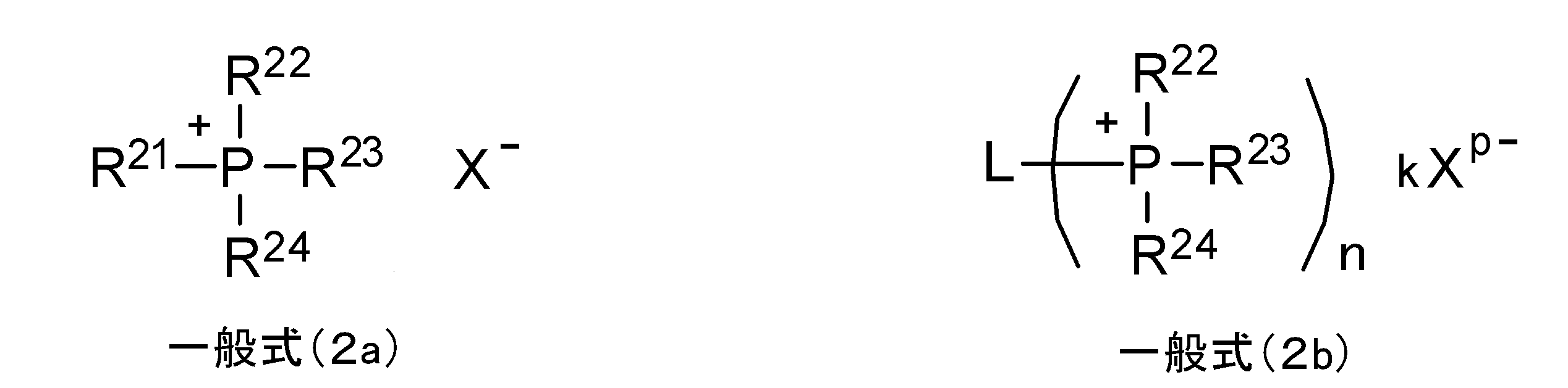
一般式(2a)中、X-は対アニオンを表す。R21~R24は、それぞれ独立にアルキル基、アリール基、又はヘテロアリール基を表す。R21~R24から選ばれる任意の2つの基は互いに結合して環を形成してもよい。
一般式(2b)中、nは2又は3の整数を表す。Xp-はp価の対アニオンを表し、pは1~3の整数を表す。kは1~3の整数を表す。但し、n=kpである。Lはn価の連結基又は単結合を表す。R22~R24は、一般式(2a)と同義である。複数のR22~R24は、同じであっても異なってもよい。
一般式(2b)中、nは2又は3の整数を表す。Xp-はp価の対アニオンを表し、pは1~3の整数を表す。kは1~3の整数を表す。但し、n=kpである。Lはn価の連結基又は単結合を表す。R22~R24は、一般式(2a)と同義である。複数のR22~R24は、同じであっても異なってもよい。

一般式(3a)中、X-は対アニオンを表す。Aは含窒素ヘテロ環基を表す。R31とR32は、それぞれ独立にアルキル基、アリール基、又はヘテロアリール基を表す。R31はAと結合して環を形成してもよい。mは0又は1を表し、Aが含窒素芳香族ヘテロ環基の場合、mは0であり、Aが含窒素脂肪族ヘテロ環基の場合、mは1である。
一般式(3b)中、nは2又は3の整数を表す。Xp-はp価の対アニオンを表し、pは1~3の整数を表す。kは1~3の整数を表す。但し、n=kpである。Lはn価の連結基又は単結合を表す。A、R32、mは、一般式(3a)と同義である。複数のA、R32は、同じであっても異なってもよい。
一般式(3b)中、nは2又は3の整数を表す。Xp-はp価の対アニオンを表し、pは1~3の整数を表す。kは1~3の整数を表す。但し、n=kpである。Lはn価の連結基又は単結合を表す。A、R32、mは、一般式(3a)と同義である。複数のA、R32は、同じであっても異なってもよい。
<2> 一般式(1a)及び(1b)において、R11~R13がアルキル基である、<1>記載の熱電変換素子。
<3> 一般式(2a)及び(2b)において、R21~R24がアルキル基である、<1>記載の熱電変換素子。
<4> 一般式(3a)及び(3b)において、Aが含窒素芳香族ヘテロ環基である、<1>記載の熱電変換素子。
<5> 一般式(1a)~(3b)において、X-又はXp-が強酸の共役塩基である、<1>~<4>のいずれか1項に記載の熱電変換素子。
<6> 一般式(1a)~(3b)で表される化合物の融点が100℃以下である、<1>~<5>のいずれか1項に記載の熱電変換素子。
<7> 熱電変換層におけるナノ導電性材料と一般式(1a)~(3b)で表される化合物との含有比率が、質量基準で1:9~9:1である、<1>~<6>のいずれか1項に記載の熱電変換素子。
<8> ナノ導電性材料が、カーボンナノチューブである、<1>~<7>のいずれか1項に記載の熱電変換素子。
<9> 第1の電極及び第2の電極が、各々独立に、アルミニウム、金、銀又は銅で形成されてなる、<1>~<8>のいずれか1項に記載に記載の熱電変換素子。
<10> 熱電変換層に共役高分子を含む、<1>~<9>のいずれか1項に記載の熱電変換素子。
<11> <1>~<10>のいずれか1項に記載の熱電変換素子を用いた熱電発電用物品。
<12> <1>~<10>のいずれか1項に記載の熱電変換素子を用いたセンサー用電源。
<13> ナノ導電性材料及び下記一般式(1a)~(3b)の化合物から選択される少なくとも1種の化合物を含有する、熱電変換素子の熱電変換層を形成するための熱電変換材料。
<14> 有機溶媒を含む<13>記載の熱電変換材料。
<15> ナノ導電性材料を有機溶媒中に分散してなる<14>記載の熱電変換材料。
<3> 一般式(2a)及び(2b)において、R21~R24がアルキル基である、<1>記載の熱電変換素子。
<4> 一般式(3a)及び(3b)において、Aが含窒素芳香族ヘテロ環基である、<1>記載の熱電変換素子。
<5> 一般式(1a)~(3b)において、X-又はXp-が強酸の共役塩基である、<1>~<4>のいずれか1項に記載の熱電変換素子。
<6> 一般式(1a)~(3b)で表される化合物の融点が100℃以下である、<1>~<5>のいずれか1項に記載の熱電変換素子。
<7> 熱電変換層におけるナノ導電性材料と一般式(1a)~(3b)で表される化合物との含有比率が、質量基準で1:9~9:1である、<1>~<6>のいずれか1項に記載の熱電変換素子。
<8> ナノ導電性材料が、カーボンナノチューブである、<1>~<7>のいずれか1項に記載の熱電変換素子。
<9> 第1の電極及び第2の電極が、各々独立に、アルミニウム、金、銀又は銅で形成されてなる、<1>~<8>のいずれか1項に記載に記載の熱電変換素子。
<10> 熱電変換層に共役高分子を含む、<1>~<9>のいずれか1項に記載の熱電変換素子。
<11> <1>~<10>のいずれか1項に記載の熱電変換素子を用いた熱電発電用物品。
<12> <1>~<10>のいずれか1項に記載の熱電変換素子を用いたセンサー用電源。
<13> ナノ導電性材料及び下記一般式(1a)~(3b)の化合物から選択される少なくとも1種の化合物を含有する、熱電変換素子の熱電変換層を形成するための熱電変換材料。
<14> 有機溶媒を含む<13>記載の熱電変換材料。
<15> ナノ導電性材料を有機溶媒中に分散してなる<14>記載の熱電変換材料。
本発明において、「~」を用いて表される数値範囲は、「~」の前後に記載される数値を下限値および上限値として含む範囲を意味する。
また、本発明において、置換基に関してxxx基というときには、そのxxx基に任意の置換基を有していてもよい。また、同一の符号で示された基が複数ある場合は、互いに同じであっても異なっていてもよい。
各式で示される繰り返し構造は、まったく同じ繰り返し構造でなくとも、式に示される範囲であれば、異なった繰り返し構造をも含む。例えば、繰り返し構造がアルキル基を有する場合、各式で示される繰り返し構造は、メチル基を有する繰り返し構造のみでもよく、メチル基を有する繰り返し構造に加えて、他のアルキル基、例えばエチル基を有する繰り返し構造を含んでいてもよい。
また、本発明において、置換基に関してxxx基というときには、そのxxx基に任意の置換基を有していてもよい。また、同一の符号で示された基が複数ある場合は、互いに同じであっても異なっていてもよい。
各式で示される繰り返し構造は、まったく同じ繰り返し構造でなくとも、式に示される範囲であれば、異なった繰り返し構造をも含む。例えば、繰り返し構造がアルキル基を有する場合、各式で示される繰り返し構造は、メチル基を有する繰り返し構造のみでもよく、メチル基を有する繰り返し構造に加えて、他のアルキル基、例えばエチル基を有する繰り返し構造を含んでいてもよい。
本発明の熱電変換材料は、ナノ導電性材料の分散性がよく、高い熱起電力を備える。当該材料を熱電変換層に用いた本発明の熱変換素子は、熱電変換層と電極との密着性に優れ、高い熱電変換性能を発揮する。
また、当該熱電変換素子を用いた本発明の熱電発電用物品およびセンサー用電源等は、優れた熱電変換性能を発揮する。
また、当該熱電変換素子を用いた本発明の熱電発電用物品およびセンサー用電源等は、優れた熱電変換性能を発揮する。
本発明の上記及び他の特徴及び利点は、適宜添付の図面を参照して、下記の記載からより明らかになるであろう。
本発明の熱電変換素子は、基材上に、第1の電極、熱電変換層および第2の電極を有する。該熱電変換層は、ナノ導電性材料、及び下記一般式(1a)~(3b)で表される化合物から選択される少なくとも1種の化合物を含有する本発明の熱電変換材料によって基材上に成形されている。
本発明の熱電変換素子の熱電変換性能は、下記式(A)で示される性能指数ZTにより表すことができる。
性能指数ZT=S2・σ・T/κ (A)
式(A)において、 S(V/K):絶対温度1K当りの熱起電力(ゼーベック係数)
σ(S/m):導電率
κ(W/mK):熱伝導率
T(K):絶対温度
性能指数ZT=S2・σ・T/κ (A)
式(A)において、 S(V/K):絶対温度1K当りの熱起電力(ゼーベック係数)
σ(S/m):導電率
κ(W/mK):熱伝導率
T(K):絶対温度
上記式(A)から明らかなように、熱電変換性能の向上には、熱起電力S及び導電率σを高めるとともに、熱伝導率κを下げることが重要となる。このように熱電変換性能には、導電率σ以外のファクターが大きく影響するため、一般的に導電率σが高いとされる材料であっても、熱電変換材料として有効に機能するかは実際のところ未知数である。
また、上述のように、熱電変換素子は、腕時計や僻地用電源、宇宙用電源等に使用されるものであるから、初期の熱電変換性能を長期にわたって維持できることも求められている。
また、上述のように、熱電変換素子は、腕時計や僻地用電源、宇宙用電源等に使用されるものであるから、初期の熱電変換性能を長期にわたって維持できることも求められている。
また、熱電変換素子は、熱電変換層の厚さ方向または面方向に温度差が生じている状態で、厚さ方向または面方向に温度差を伝達するように機能するため、熱電変換材料をある程度の厚みを持った形状に成形して熱電変換層を形成する必要がある。そのため、熱電変換層を塗布により成膜する場合には、熱電変換材料には良好な塗布性や成膜性が要求される。本発明の熱電変換材料は、ナノ導電性材料の分散性が良好で塗布性や成膜性においても優れ、熱電変換層への成形・加工に適する。
以下、本発明の熱電変換材料、次いで本発明の熱電変換素子等について、説明する。
[熱電変換材料]
本発明の熱電変換材料は、熱電変換素子の熱電変換層を形成するための熱電変換組成物であって、ナノ導電性材料及び下記一般式(1a)~(3b)で表される化合物から選択される少なくとも1種の化合物を含有している。
本発明の熱電変換材料は、熱電変換素子の熱電変換層を形成するための熱電変換組成物であって、ナノ導電性材料及び下記一般式(1a)~(3b)で表される化合物から選択される少なくとも1種の化合物を含有している。
まず、本発明の熱電変換材料に用いる各成分について説明する。
<ナノ導電性材料>
本発明に用いるナノ導電性材料は、少なくとも一辺がナノメートルサイズの大きさで、導電性を有する材料であればよく、ナノメートルサイズの大きさの導電性を有する炭素材料(以下、ナノ炭素材料ということがある)、ナノメートルサイズの大きさの金属材料(以下、ナノ金属材料ということがある)等が挙げられる。
本発明に用いるナノ導電性材料は、ナノ炭素材料およびナノ金属材料の中でも、それぞれ後述する、カーボンナノチューブ、カーボンナノファイバー、フラーレン、グラファイト、グラフェンおよびカーボンナノ粒子のナノ炭素材料、ならびに、金属ナノワイヤーが好ましく、導電性向上および溶媒中での分散性向上の観点で、カーボンナノチューブが特に好ましい。
本発明に用いるナノ導電性材料は、少なくとも一辺がナノメートルサイズの大きさで、導電性を有する材料であればよく、ナノメートルサイズの大きさの導電性を有する炭素材料(以下、ナノ炭素材料ということがある)、ナノメートルサイズの大きさの金属材料(以下、ナノ金属材料ということがある)等が挙げられる。
本発明に用いるナノ導電性材料は、ナノ炭素材料およびナノ金属材料の中でも、それぞれ後述する、カーボンナノチューブ、カーボンナノファイバー、フラーレン、グラファイト、グラフェンおよびカーボンナノ粒子のナノ炭素材料、ならびに、金属ナノワイヤーが好ましく、導電性向上および溶媒中での分散性向上の観点で、カーボンナノチューブが特に好ましい。
熱電変換材料中のナノ導電性材料の含有量は、熱電変換性能の点で、熱電変換材料の全固形分中、すなわち熱電変換層中、10~90質量%であることが好ましく、15~85質量%であることがより好ましく、20~80質量%であることが特に好ましい。
ナノ導電性材料は、1種のみを単独で使用してもよく、2種以上を併用してもよい。ナノ導電性材料として2種以上を併用する場合には、少なくとも1種ずつのナノ炭素材料およびナノ金属材料を併用してもよく、ナノ炭素材料またはナノ金属材料それぞれを2種併用してもよい。
ナノ導電性材料は、1種のみを単独で使用してもよく、2種以上を併用してもよい。ナノ導電性材料として2種以上を併用する場合には、少なくとも1種ずつのナノ炭素材料およびナノ金属材料を併用してもよく、ナノ炭素材料またはナノ金属材料それぞれを2種併用してもよい。
1.ナノ炭素材料
ナノ炭素材料は、上述の通り、ナノメートルサイズの大きさで導電性を有する炭素材料であって、その一例を挙げると、炭素原子のsp2混成軌道で構成される炭素-炭素結合によって炭素原子同士が化学結合してなるナノメートルサイズの導電性材料等である。具体的には、フラーレン(金属内包フラーレンおよび玉葱状フラーレンを含む。)、カーボンナノチューブ(ピーポッドを含む。)、カーボンナノチューブの片側が閉じた形をしたカーボンナノホーン、カーボンナノファイバー、カーボンナノウォール、カーボンナノフィラメント、カーボンナノコイル、気相成長カーボン(VGCF)、グラファイト、グラフェン、カーボンナノ粒子、カーボンナノチューブの頭部に穴があいたコップ型のナノカーボン物質等が挙げられる。また、ナノ炭素材料として、グラファイト型の結晶構造を持ち導電性を示す各種カーボンブラックも用いることができ、例えば、ケッチェンブラック、アセチレンブラック等が挙げられ、具体的には、商品名「バルカン」等のカーボンブラックが挙げられる。
ナノ炭素材料は、上述の通り、ナノメートルサイズの大きさで導電性を有する炭素材料であって、その一例を挙げると、炭素原子のsp2混成軌道で構成される炭素-炭素結合によって炭素原子同士が化学結合してなるナノメートルサイズの導電性材料等である。具体的には、フラーレン(金属内包フラーレンおよび玉葱状フラーレンを含む。)、カーボンナノチューブ(ピーポッドを含む。)、カーボンナノチューブの片側が閉じた形をしたカーボンナノホーン、カーボンナノファイバー、カーボンナノウォール、カーボンナノフィラメント、カーボンナノコイル、気相成長カーボン(VGCF)、グラファイト、グラフェン、カーボンナノ粒子、カーボンナノチューブの頭部に穴があいたコップ型のナノカーボン物質等が挙げられる。また、ナノ炭素材料として、グラファイト型の結晶構造を持ち導電性を示す各種カーボンブラックも用いることができ、例えば、ケッチェンブラック、アセチレンブラック等が挙げられ、具体的には、商品名「バルカン」等のカーボンブラックが挙げられる。
これらのナノ炭素材料は、従来の製造方法によって製造できる。具体的には、二酸化炭素の接触水素還元、アーク放電法、レーザー蒸発法、CVD法、気相成長法、気相流動法、一酸化炭素を高温高圧化で鉄触媒と共に反応させて気相で成長させるHiPco法、オイルファーネス法等が挙げられる。このようにして製造されたナノ炭素材料は、そのまま用いることもでき、また、洗浄、遠心分離、ろ過、酸化、クロマトグラフ等によって精製されたものを用いることもできる。さらに、ナノ炭素材料は、必要に応じて、ボールミル、振動ミル、サンドミル、ロールミル等のボール型混練装置等を用いて粉砕したもの、化学的、物理的処理によって短く切断されたもの等を用いることもできる。
本発明で用いるナノ導電性材料のサイズはナノメートルサイズであれば特に限定されない。ナノ導電性材料が、カーボンナノチューブ、カーボンナノホーン、カーボンナノファイバー、カーボンナノフィラメント、カーボンナノコイル、気相成長カーボン(VGCF)、コップ型のナノカーボン物質等である場合、特にカーボンナノチューブである場合、平均長さは特に限定されないが、製造容易性、成膜性、導電性等の観点から、0.01~1000μmであることが好ましく、0.1~100μmであることがより好ましい。また、直径は特に限定されないが、耐久性、透明性、成膜性、導電性等の観点から、0.4~100nmであることが好ましく、より好ましくは50nm以下、さらに好ましくは15nm以下である。
ナノ炭素材料は、上述の中でも、カーボンナノチューブ、カーボンナノファイバー、グラファイト、グラフェンおよびカーボンナノ粒子が好ましく、カーボンナノチューブが特に好ましい。
以下、カーボンナノチューブ(以下、CNTともいう)について説明する。CNTは、1枚の炭素膜(グラフェン・シート)が円筒状に巻かれた単層CNT、2枚のグラフェン・シートが同心円状に巻かれた2層CNT、および複数のグラフェン・シートが同心円状に巻かれた多層CNTがある。本発明においては、単層CNT、2層CNT、多層CNTを各々単独で用いてもよく、2種以上を併せて用いてもよい。特に、導電性および半導体特性において優れた性質を持つ単層CNTおよび2層CNTを用いることが好ましく、単層CNTを用いることがより好ましい。
単層CNTの場合、グラフェンシートのグラフェンの六角形の向きに基づく螺旋構造の対称性を軸性カイラルといい、グラフェン上のある6員環の基準点からの2次元格子ベクトルのことをカイラルベクトルという。このカイラルベクトルを指数化した(n,m)をカイラル指数といい、このカイラル指数によって金属性と半導体性に分かれる。具体的には、n-mが3の倍数であるものが金属性を示し、3の倍数でないものが半導体性を示す。
本発明で用いる単層CNTは、半導体性のものであっても、金属性のものであってもよく、両者を併せて用いてもよい。また、CNTには金属等が内包されていてもよく、フラーレン等の分子が内包されたもの(特にフラーレンを内包したものをピーポッドという)を用いてもよい。
単層CNTの場合、グラフェンシートのグラフェンの六角形の向きに基づく螺旋構造の対称性を軸性カイラルといい、グラフェン上のある6員環の基準点からの2次元格子ベクトルのことをカイラルベクトルという。このカイラルベクトルを指数化した(n,m)をカイラル指数といい、このカイラル指数によって金属性と半導体性に分かれる。具体的には、n-mが3の倍数であるものが金属性を示し、3の倍数でないものが半導体性を示す。
本発明で用いる単層CNTは、半導体性のものであっても、金属性のものであってもよく、両者を併せて用いてもよい。また、CNTには金属等が内包されていてもよく、フラーレン等の分子が内包されたもの(特にフラーレンを内包したものをピーポッドという)を用いてもよい。
CNTはアーク放電法、化学気相成長法(以下、CVD法という)、レーザー・アブレーション法等によって製造することができる。本発明に用いられるCNTは、いずれの方法によって得られたものであってもよいが、好ましくはアーク放電法およびCVD法により得られたものである。
CNTを製造する際には、同時にフラーレンやグラファイト、非晶性炭素が副生成物として生じることがある。これら副生成物を除去するために精製してもよい。CNTの精製方法は特に限定されないが、上述の精製法の他に、硝酸、硫酸等による酸処理、超音波処理が不純物の除去には有効である。併せて、フィルターによる分離除去を行うことも、純度を向上させる観点からより好ましい。
CNTを製造する際には、同時にフラーレンやグラファイト、非晶性炭素が副生成物として生じることがある。これら副生成物を除去するために精製してもよい。CNTの精製方法は特に限定されないが、上述の精製法の他に、硝酸、硫酸等による酸処理、超音波処理が不純物の除去には有効である。併せて、フィルターによる分離除去を行うことも、純度を向上させる観点からより好ましい。
精製の後、得られたCNTをそのまま用いることもできる。また、CNTは一般に紐状で生成されるため、用途に応じて所望の長さにカットして用いてもよい。CNTは、硝酸、硫酸等による酸処理、超音波処理、凍結粉砕法等により短繊維状にカットすることができる。また、併せてフィルターによる分離を行うことも、純度を向上させる観点から好ましい。
本発明においては、カットしたCNTだけではなく、あらかじめ短繊維状に作製したCNTも同様に使用できる。このような短繊維状CNTは、例えば、基板上に鉄、コバルト等の触媒金属を形成し、その表面にCVD法により700~900℃で炭素化合物を熱分解してCNTを気相成長させることによって、基板表面に垂直方向に配向した形状で得られる。このようにして作製された短繊維状CNTは基板から剥ぎ取る等の方法で取り出すことができる。また、短繊維状CNTはポーラスシリコンのようなポーラスな支持体や、アルミナの陽極酸化膜上に触媒金属を担持させ、その表面にCNTをCVD法にて成長させることもできる。触媒金属を分子内に含む鉄フタロシアニンのような分子を原料とし、アルゴン/水素のガス流中でCVDを行うことによって基板上にCNTを作製する方法でも配向した短繊維状のCNTを作製することもできる。さらには、エピタキシャル成長法によってSiC単結晶表面に配向した短繊維状CNTを得ることもできる。
本発明においては、カットしたCNTだけではなく、あらかじめ短繊維状に作製したCNTも同様に使用できる。このような短繊維状CNTは、例えば、基板上に鉄、コバルト等の触媒金属を形成し、その表面にCVD法により700~900℃で炭素化合物を熱分解してCNTを気相成長させることによって、基板表面に垂直方向に配向した形状で得られる。このようにして作製された短繊維状CNTは基板から剥ぎ取る等の方法で取り出すことができる。また、短繊維状CNTはポーラスシリコンのようなポーラスな支持体や、アルミナの陽極酸化膜上に触媒金属を担持させ、その表面にCNTをCVD法にて成長させることもできる。触媒金属を分子内に含む鉄フタロシアニンのような分子を原料とし、アルゴン/水素のガス流中でCVDを行うことによって基板上にCNTを作製する方法でも配向した短繊維状のCNTを作製することもできる。さらには、エピタキシャル成長法によってSiC単結晶表面に配向した短繊維状CNTを得ることもできる。
2.ナノ金属材料
ナノ金属材料は、ナノメートルサイズの繊維状または粒子状の金属材料等であり、具体的には、繊維状の金属材料(金属繊維ともいう)、粒子状の金属材料(金属ナノ粒子ともいう)等が挙げられる。ナノ金属材料は、後述する金属ナノワイヤーが好ましい。
ナノ金属材料は、ナノメートルサイズの繊維状または粒子状の金属材料等であり、具体的には、繊維状の金属材料(金属繊維ともいう)、粒子状の金属材料(金属ナノ粒子ともいう)等が挙げられる。ナノ金属材料は、後述する金属ナノワイヤーが好ましい。
金属繊維は、中実構造または中空構造であるのが好ましい。平均短軸長さが1~1,000nmであって平均長軸長さが1~100μmの中実構造を持つ金属繊維を金属ナノワイヤーといい、平均短軸長さが1~1,000nm、平均長軸長さが0.1~1,000μmであって中空構造を持つ金属繊維を金属ナノチューブという。
金属繊維の材料としては、導電性を有する金属であればよく、目的に応じて適宜選択することができ、例えば、長周期律表(国際純正および応用化学連合(IUPAC)、1991改訂)の第4周期、第5周期および第6周期からなる群から選ばれる少なくとも1種の金属が好ましく、第2族~第14族から選ばれる少なくとも1種の金属がより好ましく、第2族、第8族、第9族、第10族、第11族、第12族、第13族、および第14族から選ばれる少なくとも1種の金属が更に好ましい。
このような金属として、例えば、銅、銀、金、白金、パラジウム、ニッケル、錫、コバルト、ロジウム、イリジウム、鉄、ルテニウム、オスミウム、マンガン、モリブデン、タングステン、ニオブ、タンテル、チタン、ビスマス、アンチモン、鉛、またはこれらの合金等が挙げられる。これらの中でも、導電性に優れる点で、銀、および銀との合金が好ましい。銀との合金で使用する金属としては、白金、オスミウム、パラジウム、イリジウム等が挙げられる。金属は、1種単独で使用してもよく、2種以上を併用してもよい。
このような金属として、例えば、銅、銀、金、白金、パラジウム、ニッケル、錫、コバルト、ロジウム、イリジウム、鉄、ルテニウム、オスミウム、マンガン、モリブデン、タングステン、ニオブ、タンテル、チタン、ビスマス、アンチモン、鉛、またはこれらの合金等が挙げられる。これらの中でも、導電性に優れる点で、銀、および銀との合金が好ましい。銀との合金で使用する金属としては、白金、オスミウム、パラジウム、イリジウム等が挙げられる。金属は、1種単独で使用してもよく、2種以上を併用してもよい。
金属ナノワイヤーは、上述の金属で中空構造に形成されていれば、その形状は特に限定されず、目的に応じて適宜選択することができる。例えば、円柱状、直方体状、断面が多角形となる柱状など任意の形状をとることができ、熱電変換層の透明性が高くなる点で、円柱状、断面の多角形の角が丸まっている断面形状が好ましい。金属ナノワイヤーの断面形状は、透過型電子顕微鏡(TEM)で観察することにより調べることができる。
金属ナノワイヤーの平均短軸長さ(「平均短軸径」または「平均直径」と称することがある)は、上述のナノ導電性材料と同じ観点から、50nm以下が好ましく、1~50nmがより好ましく、10~40nmがさらに好ましく、15~35nmが特に好ましい。平均短軸長さは、例えば透過型電子顕微鏡(TEM;日本電子株式会社製、JEM-2000FX)を用い、300個の金属ナノワイヤーの短軸長さを求め、これらの平均値として算出できる。なお、金属ナノワイヤーの短軸が円形でない場合の短軸長さは、最も長いものを短軸長さとする。
金属ナノワイヤーの平均長軸長さ(平均長さと称することがある)は、同様に、1μm以上が好ましく、1~40μmがより好ましく、3~35μmがさらに好ましく、5~30μmが特に好ましい。平均長軸長さは、例えば透過型電子顕微鏡(TEM;日本電子株式会社製、JEM-2000FX)を用い、300個の金属ナノワイヤーの長軸長さを求め、これらの平均値として算出できる。なお、金属ナノワイヤーが曲がっている場合、それを弧とする円を考慮し、その半径および曲率から算出される値を長軸長さとする。
金属ナノワイヤーの平均長軸長さ(平均長さと称することがある)は、同様に、1μm以上が好ましく、1~40μmがより好ましく、3~35μmがさらに好ましく、5~30μmが特に好ましい。平均長軸長さは、例えば透過型電子顕微鏡(TEM;日本電子株式会社製、JEM-2000FX)を用い、300個の金属ナノワイヤーの長軸長さを求め、これらの平均値として算出できる。なお、金属ナノワイヤーが曲がっている場合、それを弧とする円を考慮し、その半径および曲率から算出される値を長軸長さとする。
金属ナノワイヤーは、いかなる製造方法で製造してもよいが、特開2012-230881号公報に記載されている、ハロゲン化合物と分散添加剤とを溶解した溶媒中で加熱しながら金属イオンを還元する製造方法で製造するのが好ましい。ハロゲン化合物、分散添加剤および溶媒ならびに加熱条件等の詳細は特開2012-230881号公報に記載されている。また、この製造方法以外にも、例えば、特開2009-215594号公報、特開2009-242880号公報、特開2009-299162号公報、特開2010-84173号公報、特開2010-86714号公報等にそれぞれ記載の製造方法によって、金属ナノワイヤーを製造することもできる。
金属ナノチューブは、上述の金属で中空構造に形成されていれば、その形状は特に限定されず、単層であっても多層であってもよい。導電性および熱伝導性に優れる点で、金属ナノチューブは単層であるのが好ましい。
金属ナノチューブの厚み(外径と内径との差)は、耐久性、透明性、成膜性、導電性等の観点から、3~80nmが好ましく、3~30nmがより好ましい。金属ナノチューブの平均長軸長さは、上述のナノ導電性材料と同じ観点から、1~40μmが好ましく、3~35μmがより好ましく、5~30μmがさらに好ましい。金属ナノチューブの平均短軸長さは金属ナノワイヤーの平均短軸長さと同様であるのが好ましい。
金属ナノチューブの厚み(外径と内径との差)は、耐久性、透明性、成膜性、導電性等の観点から、3~80nmが好ましく、3~30nmがより好ましい。金属ナノチューブの平均長軸長さは、上述のナノ導電性材料と同じ観点から、1~40μmが好ましく、3~35μmがより好ましく、5~30μmがさらに好ましい。金属ナノチューブの平均短軸長さは金属ナノワイヤーの平均短軸長さと同様であるのが好ましい。
金属ナノチューブは、いかなる製造方法で製造してもよく、例えば、米国特許出願公開第2005/0056118号明細書に記載の製造方法等で製造することができる。
金属ナノ粒子は、上述の金属で形成された、粒子状または粉末状の金属微粒子であればよく、金属微粒子、金属微粒子の表面を保護剤で被覆したものでもよく、さらに、表面を被覆したものを分散媒体中に分散させたものでもよい。金属ナノ粒子に使用される金属としては、上述した中でも、銀、銅、金、パラジウム、ニッケル、ロジウムなどが好ましく挙げられる。また、これらの少なくとも2種からなる合金、これらの少なくとも1種と鉄との合金等も使用できる。2種からなる合金としては、例えば、白金-金合金、白金-パラジウム合金、金-銀合金、銀-パラジウム合金、パラジウム-金合金、白金-金合金、ロジウム-パラジウム合金、銀-ロジウム合金、銅-パラジウム合金、ニッケル-パラジウム合金等が挙げられる。また、鉄との合金としては、例えば、鉄-白金合金、鉄-白金-銅合金、鉄-白金-スズ合金、鉄-白金-ビスマス合金および鉄-白金-鉛合金等が挙げられる。これらの金属または合金は、単独でまたは2種以上組み合わせて用いることができる。
金属ナノ粒子の平均粒径(動的光散乱法)は、導電性に優れる点で、1~150nmが好ましい。
金属微粒子の保護剤は、例えば、特開2012-222055号公報に記載の保護剤が好適に挙げられ、炭素数10~20の直鎖状または分枝状のアルキル鎖を有する保護剤、特に脂肪酸類または脂肪族アミン類、脂肪族チオール類もしくは脂肪族アルコール類等がさらに好適に挙げられる。ここで、炭素数が10~20であると、金属ナノ粒子の保存安定性が高く、かつ導電性にも優れる。脂肪酸類脂肪族アミン類、脂肪族チオール類および脂肪族アルコール類は、特開2012-222055号公報に記載のものが好適である。
金属ナノ粒子は、いかなる製造方法で製造されてもよく、製造方法として、例えば、ガス中蒸着法、スパッタリング法、金属蒸気合成法、コロイド法、アルコキシド法、共沈法、均一沈殿法、熱分解法、化学還元法、アミン還元法および溶媒蒸発法等が挙げられる。これら製造方法は、それぞれ特有の特徴を備えるが、特に大量生産を目的とする場合には化学還元法、アミン還元法を用いるのが好ましい。これらの製造方法を実施するに当たっては、必要に応じて上述の保護剤を選択して使用するほか、公知の還元剤等を適宜用いることができる。
<一般式(1a)~(3b)で表される化合物>
本発明の熱電変換材料は、上述のナノ導電性材料に加え、下記一般式(1a)~(3b)で表される化合物から選択される少なくとも1種の化合物を含有する。熱電変換材料にナノ導電性材料と共に一般式(1a)~(3b)で表される化合物を用いることで、ナノ導電性材料の分散性が向上し、熱電変換層と電極との密着性、及び熱電変換性能に優れた熱電変換素子が得られる。
本発明の熱電変換材料は、上述のナノ導電性材料に加え、下記一般式(1a)~(3b)で表される化合物から選択される少なくとも1種の化合物を含有する。熱電変換材料にナノ導電性材料と共に一般式(1a)~(3b)で表される化合物を用いることで、ナノ導電性材料の分散性が向上し、熱電変換層と電極との密着性、及び熱電変換性能に優れた熱電変換素子が得られる。
熱電変換材料中の、ナノ導電性材料と一般式(1a)~(3b)で表される化合物との含有比率は、質量基準で1:9~9:1であることが好ましく、2:8~8:2であることがより好ましい。両者の含有比率を上記範囲内とすることで、材料の塗布性や成膜性が向上する。
ナノ導電性材料と共に前記一般式(1a)~(3b)で表される化合物を用いることで、電極との密着性及び熱電変換性能が向上する機序は定かではないが、下記のメカニズムによって、熱電変換層におけるナノ導電性材料の分散性が向上するためではないかと推測される。
ナノ導電性材料の分散性が悪いと、熱電変換材料を電極上に塗布・成膜したときに、膜厚ムラや部分凝集等が生じやすく、均一な膜の形成が難しい。その結果、膜と電極との密着性が低下する。これは、成膜後の乾燥過程で、材料中の分散媒が減少するのに伴ってナノ導電性材料の濃度が高まり、十分に分散されていないナノ導電性材料を核として再凝集が起こるためと考えられる。
一方、ナノ導電性材料の分散性がよい場合は、このような再凝集は起こりにくく、結果として、膜厚ムラや部分凝集等がない均一な膜を形成できる、電極との密着性が良化する。
本発明の熱電変換材料において、カチオン部に硫黄原子を有する前記一般式(1a)又は(1b)で表される化合物、及びカチオン部にリン原子を有する前記一般式(2a)又は(2b)で表される化合物では、カチオン部の空のd軌道とナノ導電性材料が電子的に相互作用することにより、ナノ導電性材料の凝集状態をほぐし、分散性が向上する。硫黄原子やリン原子は、酸素原子や窒素原子に比べて原子半径が大きいため、アルキル基等が置換している場合であっても、比較的ナノ導電性材料と相互作用しやすいと考えられる。また、前記一般式(3a)又は(3b)で表される化合物は、カチオン部に含窒素へテロ環構造を有しており、これがナノ導電性材料と電子的に相互作用することにより、ナノ導電性材料の凝集状態をほぐし、分散性が向上する。
ナノ導電性材料の分散性が悪いと、熱電変換材料を電極上に塗布・成膜したときに、膜厚ムラや部分凝集等が生じやすく、均一な膜の形成が難しい。その結果、膜と電極との密着性が低下する。これは、成膜後の乾燥過程で、材料中の分散媒が減少するのに伴ってナノ導電性材料の濃度が高まり、十分に分散されていないナノ導電性材料を核として再凝集が起こるためと考えられる。
一方、ナノ導電性材料の分散性がよい場合は、このような再凝集は起こりにくく、結果として、膜厚ムラや部分凝集等がない均一な膜を形成できる、電極との密着性が良化する。
本発明の熱電変換材料において、カチオン部に硫黄原子を有する前記一般式(1a)又は(1b)で表される化合物、及びカチオン部にリン原子を有する前記一般式(2a)又は(2b)で表される化合物では、カチオン部の空のd軌道とナノ導電性材料が電子的に相互作用することにより、ナノ導電性材料の凝集状態をほぐし、分散性が向上する。硫黄原子やリン原子は、酸素原子や窒素原子に比べて原子半径が大きいため、アルキル基等が置換している場合であっても、比較的ナノ導電性材料と相互作用しやすいと考えられる。また、前記一般式(3a)又は(3b)で表される化合物は、カチオン部に含窒素へテロ環構造を有しており、これがナノ導電性材料と電子的に相互作用することにより、ナノ導電性材料の凝集状態をほぐし、分散性が向上する。
<一般式(1a)及び(1b)で表される化合物>
まず、下記一般式(1a)及び(1b)で表される化合物について説明する。
まず、下記一般式(1a)及び(1b)で表される化合物について説明する。
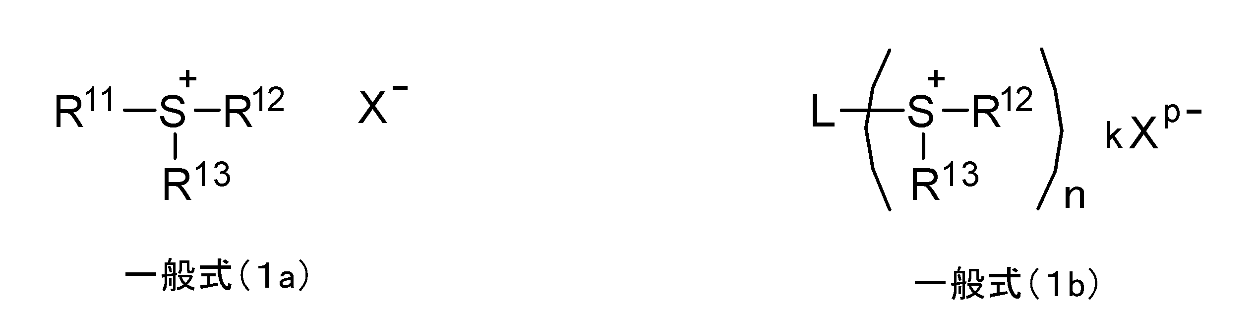
一般式(1a)中、X-は対アニオンを表す。R11~R13は、それぞれ独立にアルキル基又はヘテロアリール基を表す。R12とR13は互いに結合して環を形成してもよい。
一般式(1b)中、nは2又は3の整数を表す。Xp-はp価の対アニオンを表し、pは1~3の整数を表す。kは1~3の整数を表す。但し、n=kpである。Lはn価の連結基又は単結合を表す。R12及びR13は、一般式(1a)と同義である。複数のR12及びR13は、同じであっても異なってもよい。
一般式(1b)中、nは2又は3の整数を表す。Xp-はp価の対アニオンを表し、pは1~3の整数を表す。kは1~3の整数を表す。但し、n=kpである。Lはn価の連結基又は単結合を表す。R12及びR13は、一般式(1a)と同義である。複数のR12及びR13は、同じであっても異なってもよい。
一般式(1a)及び(1b)中、R11~R13は、それぞれ独立にアルキル基又はヘテロアリール基を表し、アルキル基が好ましい。
一般式(1a)及び(1b)においてR11~R13がそれぞれ独立にアルキル基である化合物は、可視光領域に吸収を持たないため、光によって分解されにくい。そのため、当該化合物を熱電変換層に用いた素子は、光に対する経時安定性に優れたものとなり、初期の熱電変換性能を長期にわたり維持することができる。
一般式(1a)及び(1b)においてR11~R13がそれぞれ独立にアルキル基である化合物は、可視光領域に吸収を持たないため、光によって分解されにくい。そのため、当該化合物を熱電変換層に用いた素子は、光に対する経時安定性に優れたものとなり、初期の熱電変換性能を長期にわたり維持することができる。
当該アルキル基には直鎖、分岐又は環状のアルキル基が含まれ、好ましくは直鎖アルキル基である。当該アルキル基の炭素原子数は1~14が好ましく、1~8がより好ましい。
また、当該アルキル基中に含まれるメチレン基は二価の連結基で置換されてもよく、二価の連結基としては、-O-,-S-、-COO-、-OCO-、-OCOO-、-CH=CH-,-C≡C-、-NRa-(Raは炭素原子数1~6のアルキル基を表す)が挙げられる。
当該ヘテロアリール基のヘテロ原子は窒素原子、硫黄原子、酸素原子が好ましい。また、当該ヘテロアリール基を構成する環は、5員環又は6員環が好ましく、又はこれらの縮合環も好ましい。具体的には、チオフェン環、フラン環、ピロール環、イミダゾール環、ピラゾール環、オキサゾール環、チアゾール環、オキサチアゾール環、ピリジン環、ピラジン環、ピリミジル環、ピリダジニル環、これらのベンゾ縮環体(例えばベンゾチオフェン)及びジベンゾジ縮環体(例えばジベンゾチオフェン、カルバゾール)が挙げられ、好ましくはチオフェン環、フラン環、ピロール環である。
また、当該アルキル基中に含まれるメチレン基は二価の連結基で置換されてもよく、二価の連結基としては、-O-,-S-、-COO-、-OCO-、-OCOO-、-CH=CH-,-C≡C-、-NRa-(Raは炭素原子数1~6のアルキル基を表す)が挙げられる。
当該ヘテロアリール基のヘテロ原子は窒素原子、硫黄原子、酸素原子が好ましい。また、当該ヘテロアリール基を構成する環は、5員環又は6員環が好ましく、又はこれらの縮合環も好ましい。具体的には、チオフェン環、フラン環、ピロール環、イミダゾール環、ピラゾール環、オキサゾール環、チアゾール環、オキサチアゾール環、ピリジン環、ピラジン環、ピリミジル環、ピリダジニル環、これらのベンゾ縮環体(例えばベンゾチオフェン)及びジベンゾジ縮環体(例えばジベンゾチオフェン、カルバゾール)が挙げられ、好ましくはチオフェン環、フラン環、ピロール環である。
これらのアルキル基又はヘテロアリール基は、さらに置換基を有してもよく、下記の置換基Wが挙げられる。置換基Wとしては、ハロゲン原子(好ましくは、フッ素、塩素)、直鎖、分岐又は環状のアルキル基(炭素原子数は1~20が好ましく、4~15がより好ましい)、アリール基、ヘテロアリール基、-NH2、-NHRb、-NRbRc、-CORb、-COOH、-COORb、-OCORb、-OCOORb、-CONHRb、-CONRbRc、-OCONHRb、-OCONRbRc、-OH、-ORb、SH、-SRb、-O(CH2CH2O)lRb(Rb、Rcはそれぞれ独立に、直鎖、分岐又は環状のアルキル基、アルキニル基、アルケニル基、ヘテロアルキル基、ヘテロアルキニル基、ヘテロアルケニル基、アリール基、ヘテロアリール基を表す。lは1~3の整数を表し、2が好ましい。)が挙げられる。これらの置換基は、さらに同様の置換基で置換されていてもよい。
R12とR13は互いに結合して、R12とR13が結合する硫黄原子を含むヘテロ環を形成してもよい。形成されるヘテロ環は、芳香族環であっても脂肪族環であってもよく、脂肪族環が好ましい。また、5又は6員環であることが好ましい。具体的には、テトラヒドロチオフェン環、テトラヒドロ-2H-チオピラン環が好ましい。
一般式(1b)において、複数のR12及びR13は、同じであっても異なってもよい。
一般式(1a)及び(1b)中、X-、Xp-は対アニオンを表す。
X-又はXp-で表される対アニオンは、特に限定されないが、好ましくは強酸の共役塩基である。ここで、強酸とは、ジメチルスルホキシド(DMSO)中での酸解離定数pKaが10以下の酸をいう。
強酸の共役塩基として好ましくは、ハロゲンイオン、アリールスルホン酸アニオン、パーフルオロアルキルスルホン酸アニオン、過ハロゲン化ルイス酸アニオン、パーフルオロアルキルスルホンイミドアニオン、過ハロゲン酸アニオン、アリールボレートアニオン、パーフルオロアリールボレートアニオンが挙げられる。なかでも、過ハロゲン化ルイス酸アニオン、パーフルオロアルキルスルホンイミドアニオン、過ハロゲン酸アニオン、アリールボレートアニオン、パーフルオロアリールボレートアニオンがより好ましい。
X-又はXp-で表される対アニオンは、特に限定されないが、好ましくは強酸の共役塩基である。ここで、強酸とは、ジメチルスルホキシド(DMSO)中での酸解離定数pKaが10以下の酸をいう。
強酸の共役塩基として好ましくは、ハロゲンイオン、アリールスルホン酸アニオン、パーフルオロアルキルスルホン酸アニオン、過ハロゲン化ルイス酸アニオン、パーフルオロアルキルスルホンイミドアニオン、過ハロゲン酸アニオン、アリールボレートアニオン、パーフルオロアリールボレートアニオンが挙げられる。なかでも、過ハロゲン化ルイス酸アニオン、パーフルオロアルキルスルホンイミドアニオン、過ハロゲン酸アニオン、アリールボレートアニオン、パーフルオロアリールボレートアニオンがより好ましい。
ハロゲンイオンとして具体的には、Cl-、Br-、I-が挙げられる。
アリールスルホン酸アニオンとして具体的には、p-トルエンスルホン酸アニオン、ベンゼンスルホン酸アニオン、ナフタレンスルホン酸アニオン、ナフトキノンスルホン酸アニオン、ナフタレンジスルホン酸アニオン、アントラキノンスルホン酸アニオンが挙げられる。当該アニオンのアリール部は置換基を有してもよく、置換基としてはフルオロ基が挙げられる。
パーフルオロアルキルスルホン酸アニオンとして具体的には、CF3SO3 -、C4F9SO3 -、C8F17SO3 -が挙げられる。
過ハロゲン化ルイス酸アニオンとして具体的には、PF6 -、SbF6 -、BF4 -、AsF6 -、FeCl4 -が挙げられる。
パーフルオロアルキルスルホンイミドアニオンとして具体的には、CF3SO2-N--SO2CF3、C4F9SO2-N--SO2C4F9が挙げられる。
過ハロゲン酸アニオンとして具体的には、ClO4 -、BrO4 -、IO4 -が挙げられる。
アリールボレートアニオンとして具体的には、(C6H5)4B-、(p-CH3C6H4)4B-が挙げられる。当該アニオンのアリール部は置換基を有してもよく、置換基としてはフルオロ基が挙げられる。
パーフルオロアリールボレートアニオンとして具体的には、(C6F5)4B-が挙げられる。
アリールスルホン酸アニオンとして具体的には、p-トルエンスルホン酸アニオン、ベンゼンスルホン酸アニオン、ナフタレンスルホン酸アニオン、ナフトキノンスルホン酸アニオン、ナフタレンジスルホン酸アニオン、アントラキノンスルホン酸アニオンが挙げられる。当該アニオンのアリール部は置換基を有してもよく、置換基としてはフルオロ基が挙げられる。
パーフルオロアルキルスルホン酸アニオンとして具体的には、CF3SO3 -、C4F9SO3 -、C8F17SO3 -が挙げられる。
過ハロゲン化ルイス酸アニオンとして具体的には、PF6 -、SbF6 -、BF4 -、AsF6 -、FeCl4 -が挙げられる。
パーフルオロアルキルスルホンイミドアニオンとして具体的には、CF3SO2-N--SO2CF3、C4F9SO2-N--SO2C4F9が挙げられる。
過ハロゲン酸アニオンとして具体的には、ClO4 -、BrO4 -、IO4 -が挙げられる。
アリールボレートアニオンとして具体的には、(C6H5)4B-、(p-CH3C6H4)4B-が挙げられる。当該アニオンのアリール部は置換基を有してもよく、置換基としてはフルオロ基が挙げられる。
パーフルオロアリールボレートアニオンとして具体的には、(C6F5)4B-が挙げられる。
一般式(1b)において、nは2が好ましい。pは1又は2が好ましく、1がより好ましい。より好ましくは、kが2であり、pが1である。
Lの連結基としては、2価又は3価の脂肪族基が好ましく、アルキレン基がより好ましい。Lは、アルキレン基又は単結合が好ましい。
Lの連結基としては、2価又は3価の脂肪族基が好ましく、アルキレン基がより好ましい。Lは、アルキレン基又は単結合が好ましい。
一般式(1a)及び(1b)で表される化合物の中でも、一般式(1a)で表される化合物を用いることが好ましい。
一般式(1a)又は(1b)で表される化合物を構成するカチオンの具体例を以下に示すが、本発明はこれらに限定されるものではない。
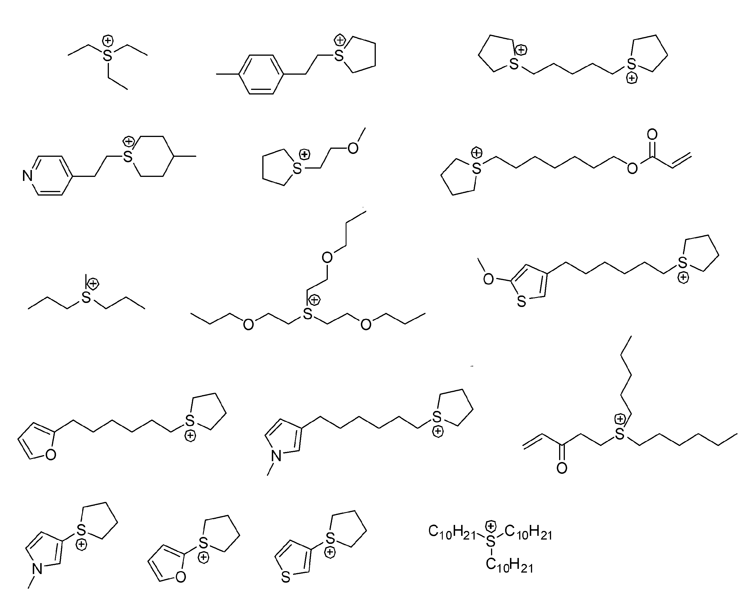
本発明の熱電変換材料には、前記一般式(1a)又は(1b)で表される化合物を、1種単独で使用してもよく、2種以上を併用してもよい。
<一般式(2a)及び(2b)で表される化合物>
次に、下記一般式(2a)及び(2b)で表される化合物について説明する。
次に、下記一般式(2a)及び(2b)で表される化合物について説明する。
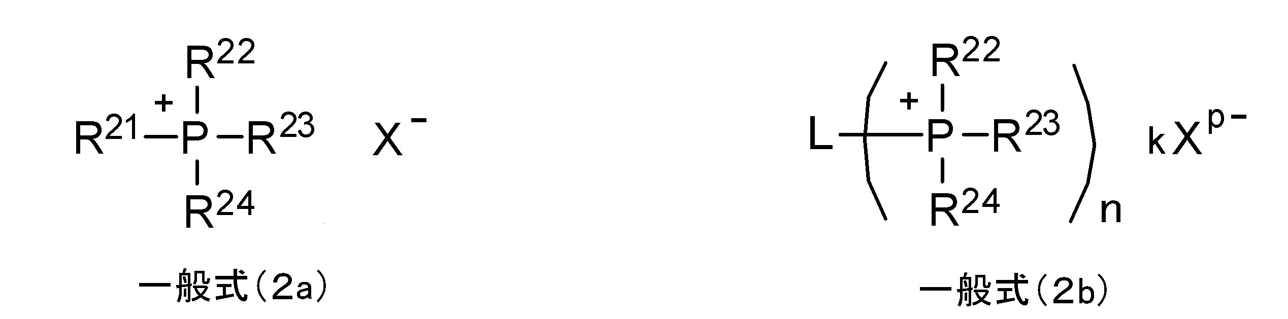
一般式(2a)中、X-は対アニオンを表す。R21~R24は、それぞれ独立にアルキル基、アリール基、又はヘテロアリール基を表す。R21~R24から選ばれる任意の2つの基は互いに結合して環を形成してもよい。
一般式(2b)中、nは2又は3の整数を表す。Xp-はp価の対アニオンを表し、pは1~3の整数を表す。kは1~3の整数を表す。但し、n=kpである。Lはn価の連結基又は単結合を表す。R22~R24は、一般式(2a)と同義である。複数のR22~R24は、同じであっても異なってもよい。
一般式(2b)中、nは2又は3の整数を表す。Xp-はp価の対アニオンを表し、pは1~3の整数を表す。kは1~3の整数を表す。但し、n=kpである。Lはn価の連結基又は単結合を表す。R22~R24は、一般式(2a)と同義である。複数のR22~R24は、同じであっても異なってもよい。
一般式(2a)及び(2b)中、R21~R24は、それぞれ独立にアルキル基、アリール基、又はヘテロアリール基を表し、アルキル基が好ましい。
一般式(2a)及び(2b)においてR21~R24がそれぞれ独立にアルキル基である化合物は、可視光領域に吸収を持たないため、光によって分解されにくい。そのため、当該化合物を熱電変換層に用いた素子は、光に対する経時安定性に優れたものとなり、初期の熱電変換性能を長期にわたり維持することができる。
一般式(2a)及び(2b)においてR21~R24がそれぞれ独立にアルキル基である化合物は、可視光領域に吸収を持たないため、光によって分解されにくい。そのため、当該化合物を熱電変換層に用いた素子は、光に対する経時安定性に優れたものとなり、初期の熱電変換性能を長期にわたり維持することができる。
当該アルキル基には直鎖、分岐又は環状のアルキル基が含まれ、好ましくは直鎖アルキル基である。当該アルキル基の炭素原子数は1~14が好ましく、1~8がより好ましい。
また、当該アルキル基中に含まれるメチレン基は二価の連結基で置換されてもよく、二価の連結基としては、-O-,-S-、-CO-、-COO-、-OCO-、-OCOO-、-CH=CH-,-C≡C-、-NRa-(Raは炭素原子数1~6のアルキル基を表す)が挙げられる。
また、当該アルキル基中に含まれるメチレン基は二価の連結基で置換されてもよく、二価の連結基としては、-O-,-S-、-CO-、-COO-、-OCO-、-OCOO-、-CH=CH-,-C≡C-、-NRa-(Raは炭素原子数1~6のアルキル基を表す)が挙げられる。
当該アリール基の炭素原子数は4~50が好ましく、6~40がより好ましい。アリール基を構成する環としては、ベンゼン環、ナフタレン環、アントラセン環、フェナントレン環、インダセン環、フルオレン環が挙げられ、好ましくはベンゼン環である。
当該ヘテロアリール基のヘテロ原子は窒素原子、硫黄原子、酸素原子が好ましい。また当該ヘテロアリール基の炭素原子数は4~50が好ましく、6~40がより好ましい。ヘテロアリール環を構成する環として具体的には、チオフェン環、フラン環、ピロール環、イミダゾール環、ピラゾール環、オキサゾール環、チアゾール環、オキサチアゾール環、ピリジン環、ピラジン環、ピリミジル環、ピリダジニル環、およびこれらのベンゾ縮環体(例えばベンゾチオフェン)およびジベンゾジ縮環体(例えばジベンゾチオフェン、カルバゾール)が挙げられ、好ましくはチオフェン環、フラン環、ピロール環である。
これらのアルキル基、アリール基、ヘテロアリール基は、置換基を有してもよく、置換基としては上記の置換基Wが挙げられる。
R21~R24から選ばれる任意の2つの基は、互いに結合して、リン原子を含むヘテロ環を形成してもよい。形成されるヘテロ環は、芳香族環であっても脂肪族環であってもよく、脂肪族環が好ましい。また、5又は6員環であることが好ましい。
一般式(2b)において、複数のR22~R24は、同じであっても異なってもよい。
一般式(2a)及び(2b)において、X-、Xp-、n、k、及びpは、一般式(1a)及び(1b)のX-、Xp-、n、k、及びpとそれぞれ同義であり、好ましい範囲も同様である。
一般式(2b)において、Lの連結基としては、2価又は3価の脂肪族基が好ましく、アルキレン基がより好ましい。Lは、アルキレン基又は単結合が好ましい。
一般式(2a)及び(2b)で表される化合物の中でも、一般式(2a)で表される化合物を用いることが好ましい。
一般式(2a)又は(2b)で表される化合物を構成するカチオンの具体例を以下に示すが、本発明はこれらに限定されるものではない。
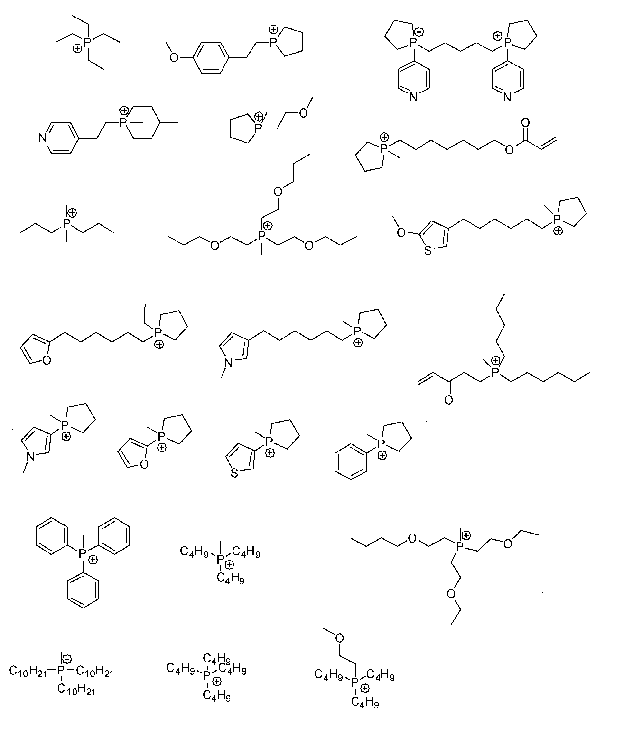
本発明の熱電変換材料には、前記一般式(2a)又は(2b)で表される化合物を、1種単独で使用してもよく、2種以上を併用してもよい。
<一般式(3a)及び(3b)で表される化合物>
次に、下記一般式(3a)及び(3b)で表される化合物について説明する。
次に、下記一般式(3a)及び(3b)で表される化合物について説明する。
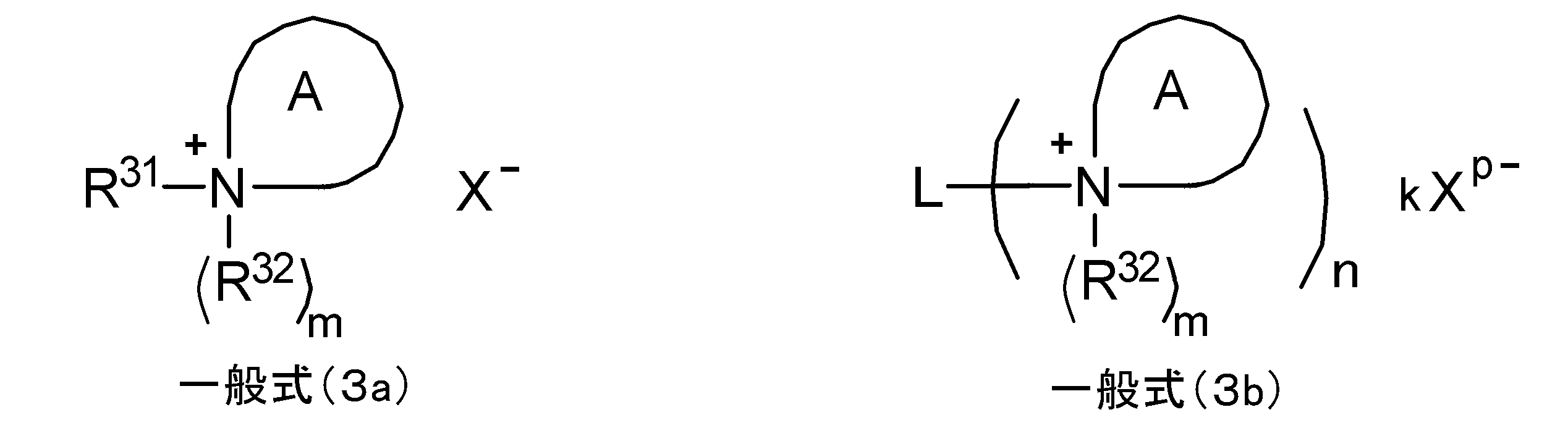
一般式(3a)中、X-は対アニオンを表す。Aは含窒素ヘテロ環基を表す。R31とR32は、それぞれ独立にアルキル基、アリール基、又はヘテロアリール基を表す。R31はAと結合して環を形成してもよい。mは0又は1を表し、Aが含窒素芳香族ヘテロ環基の場合、mは0であり、Aが含窒素脂肪族ヘテロ環基の場合、mは1である。
一般式(3b)中、nは2又は3の整数を表す。Xp-はp価の対アニオンを表し、pは1~3の整数を表す。kは1~3の整数を表す。但し、n=kpである。Lはn価の連結基又は単結合を表す。A、R32、mは、一般式(3a)と同義である。複数のA、R32は、同じであっても異なってもよい。
一般式(3b)中、nは2又は3の整数を表す。Xp-はp価の対アニオンを表し、pは1~3の整数を表す。kは1~3の整数を表す。但し、n=kpである。Lはn価の連結基又は単結合を表す。A、R32、mは、一般式(3a)と同義である。複数のA、R32は、同じであっても異なってもよい。
一般式(3a)及び(3b)中、Aは含窒素ヘテロ環基を表し、含窒素芳香族ヘテロ環であっても含窒素脂肪族ヘテロ環であってもよい。但し、Aが含窒素芳香族ヘテロ環基の場合、mは0となり、Aが含窒素脂肪族ヘテロ環基の場合、mは1となる。Aとして好ましくは、含窒素芳香族ヘテロ環基である。
一般式(3a)及び(3b)においてAが含窒素芳香族ヘテロ環基である化合物は、π電子を有しており、ナノ導電性材料の表面と電子的な相互作用(π-π相互作用)が生じる。これによりナノ導電性材料の表面に一般式(3a)又は(3b)で表される化合物が電子的に吸着して、光により酸化分解されにくい構造となる。そのため、当該化合物を熱電変換層に用いた素子は、光に対する経時安定性に優れたものとなり、初期の熱電変換性能を長期にわたり維持することができる。
一般式(3a)及び(3b)においてAが含窒素芳香族ヘテロ環基である化合物は、π電子を有しており、ナノ導電性材料の表面と電子的な相互作用(π-π相互作用)が生じる。これによりナノ導電性材料の表面に一般式(3a)又は(3b)で表される化合物が電子的に吸着して、光により酸化分解されにくい構造となる。そのため、当該化合物を熱電変換層に用いた素子は、光に対する経時安定性に優れたものとなり、初期の熱電変換性能を長期にわたり維持することができる。
Aの含窒素ヘテロ環基は、窒素原子以外のヘテロ原子を含んでもよく、当該へテロ原子として硫黄原子、酸素原子が好ましい。また、含窒素ヘテロ環基には複数の窒素原子が含まれることも好ましく、2つの窒素原子が含まれることがより好ましい。
Aの含窒素芳香族ヘテロ環基を構成する環は、5員環又は6員環が好ましく、又はこれらの縮合環も好ましい。具体的には、ピロール環、ピリジン環、イミダゾール環、チアゾール環、オキサゾール環、ピラジン環、ピリミジン環、およびこれらのベンゾ縮環体(例えばベンゾイミダゾール、インドール)およびジベンゾジ縮環体(例えばカルバゾール)が挙げられ、好ましくはピリジン環、イミダゾール環である。
Aの含窒素脂肪族ヘテロ環基を構成する環は、5員環又は6員環が好ましく、又はこれらの縮合環も好ましい。具体的には、ピロリジン環、ピペリジン環、ピペラジン環、モルホリン環、キヌクリジン環、およびこれらのベンゾ縮環体(例えばジヒドロインドール)が挙げられ、好ましいくはピロリジン環、ピペリジン環である。
これらの含窒素芳香族ヘテロ環や含窒素脂肪族ヘテロ環は、置換基を有してもよく、置換基としては上記の置換基Wが挙げられる。
Aの含窒素芳香族ヘテロ環基を構成する環は、5員環又は6員環が好ましく、又はこれらの縮合環も好ましい。具体的には、ピロール環、ピリジン環、イミダゾール環、チアゾール環、オキサゾール環、ピラジン環、ピリミジン環、およびこれらのベンゾ縮環体(例えばベンゾイミダゾール、インドール)およびジベンゾジ縮環体(例えばカルバゾール)が挙げられ、好ましくはピリジン環、イミダゾール環である。
Aの含窒素脂肪族ヘテロ環基を構成する環は、5員環又は6員環が好ましく、又はこれらの縮合環も好ましい。具体的には、ピロリジン環、ピペリジン環、ピペラジン環、モルホリン環、キヌクリジン環、およびこれらのベンゾ縮環体(例えばジヒドロインドール)が挙げられ、好ましいくはピロリジン環、ピペリジン環である。
これらの含窒素芳香族ヘテロ環や含窒素脂肪族ヘテロ環は、置換基を有してもよく、置換基としては上記の置換基Wが挙げられる。
R31とR32は、それぞれ独立にアルキル基、アリール基、又はヘテロアリール基を表し、好ましくはアルキル基である。
当該アルキル基には直鎖、分岐又は環状のアルキル基が含まれ、好ましくは直鎖アルキル基である。当該アルキル基の炭素原子数は1~14が好ましく、1~8がより好ましい。
また、当該アルキル基中に含まれるメチレン基は二価の連結基で置換されてもよく、二価の連結基としては、-O-、-S-、-CO-、-COO-、-OCO-、-OCOO-、-CH=CH-,-C≡C-、-NRa-(Raは炭素原子数1~6のアルキル基を表す)が挙げられる。
当該アルキル基には直鎖、分岐又は環状のアルキル基が含まれ、好ましくは直鎖アルキル基である。当該アルキル基の炭素原子数は1~14が好ましく、1~8がより好ましい。
また、当該アルキル基中に含まれるメチレン基は二価の連結基で置換されてもよく、二価の連結基としては、-O-、-S-、-CO-、-COO-、-OCO-、-OCOO-、-CH=CH-,-C≡C-、-NRa-(Raは炭素原子数1~6のアルキル基を表す)が挙げられる。
当該アリール基の炭素原子数は4~50が好ましく、6~40がより好ましい。アリール基を構成する環としては、ベンゼン環、ナフタレン環、アントラセン環、フェナントレン環、インダセン環、フルオレン環が挙げられ、好ましくはベンゼン環である。
当該ヘテロアリール基のヘテロ原子は窒素原子、硫黄原子、酸素原子が好ましい。また当該ヘテロアリール基の炭素原子数は4~50が好ましく、6~40がより好ましい。ヘテロアリール環を構成する環として具体的には、チオフェン環、フラン環、ピロール環、イミダゾール環、ピラゾール環、オキサゾール環、チアゾール環、オキサチアゾール環、ピリジン環、ピラジン環、ピリミジル環、ピリダジニル環、およびこれらのベンゾ縮環体(例えばベンゾチオフェン)およびジベンゾジ縮環体(例えばジベンゾチオフェン、カルバゾール)が挙げられ、好ましくはチオフェン環、フラン環、ピロール環である。
これらのアルキル基、アリール基、ヘテロアリール基は、置換基を有してもよく、置換基としては上記の置換基Wが挙げられる。
R31はAと結合して環を形成してもよい。形成されるヘテロ環としては、トリエチレンジアミン環、アザビシクロ-[4,4,0]デカン環、アザビシクロ-[2,2,2]オクタン環が好ましい。
一般式(3b)において、複数のA、R32は、同じであっても異なってもよい。
一般式(3a)及び(3b)において、X-、Xp-、n、k、及びpは、一般式(1a)及び(1b)のX-、Xp-、n、k、及びpとそれぞれ同義であり、好ましい範囲も同様である。
一般式(3b)において、Lの連結基としては、2価又は3価の脂肪族基が好ましく、アルキレン基がより好ましい。Lは、アルキレン基又は単結合が好ましい。
一般式(3a)及び(3b)で表される化合物の中でも、一般式(3a)で表される化合物を用いることが好ましい。
一般式(3a)又は(3b)で表される化合物を構成するカチオンの具体例を以下に示すが、本発明はこれらに限定されるものではない。

本発明の熱電変換材料には、前記一般式(3a)又は(3b)で表される化合物を、1種単独で使用してもよく、2種以上を併用してもよい。
前記一般式(1a)~(3b)で表される化合物は、融点が100℃以下であることが好ましい。融点を上記範囲内にする観点から、前記一般式(1a)~(3b)で表される化合物の対アニオンを、前述した強酸の共役塩基とすることが好ましい。融点が上記範囲内であると、熱電変換材料調製の際に、前記一般式(1a)~(3b)で表される化合物が分散媒(後述)によく溶解するため、材料中のナノ導電性材料の分散性がさらに向上する。その結果、当該材料により形成された熱電変換層と電極との密着性が向上し、さらには熱電変換性能も向上する。
前記一般式(1a)~(3b)で表される化合物は、市販品を用いることもでき、また、後述する実施例のようにして適宜合成してもよい。
<共役高分子>
本発明の熱電変換材料は、ナノ導電性材料および前記一般式(1a)~(3b)で表される化合物に加えて、共役高分子を含有することが好ましい。共役高分子を含有することにより、素子の熱電変換性能を更に改善できる。
本発明の熱電変換材料は、ナノ導電性材料および前記一般式(1a)~(3b)で表される化合物に加えて、共役高分子を含有することが好ましい。共役高分子を含有することにより、素子の熱電変換性能を更に改善できる。
熱電変換材料中の高分子化合物の含有率は、特に限定されないが、熱電変換性能の点から、熱電変換材料の全固形分中、すなわち熱電変換層中、10~90質量%が好ましく、20~80質量%がより好ましく、30~70質量%がさらに好ましい。
共役高分子は、主鎖がπ電子または孤立電子対のローンペアで共役する構造を有する化合物であれば特に限定されない。このような共役構造として、例えば、主鎖上の炭素-炭素結合において、一重結合と二重結合とが交互に連なる構造が挙げられる。この共役高分子は、必ずしも高分子量化合物である必要はなく、オリゴマー化合物であってもよい。
このような共役高分子としては、チオフェン系化合物、ピロール系化合物、アニリン系化合物、アセチレン系化合物、p-フェニレン系化合物、p-フェニレンビニレン系化合物、p-フェニレンエチニレン系化合物、p-フルオレニレンビニレン系化合物、フルオレン系化合物、芳香族ポリアミン系化合物(アリールアミン系化合物ともいう)、ポリアセン系化合物、ポリフェナントレン系化合物、金属フタロシアニン系化合物、p-キシリレン系化合物、ビニレンスルフィド系化合物、m-フェニレン系化合物、ナフタレンビニレン系化合物、p-フェニレンオキシド系化合物、フェニレンスルフィド系化合物、フラン系化合物、セレノフェン系化合物、アゾ系化合物、及び金属錯体系化合物からなる群より選択される少なくとも1種の化合物に対応する構成成分を繰り返し構造として含む共役高分子が挙げられる。
共役高分子が共重合体であるときは、ブロック共重合体、ランダム共重合体、交互共重合体であってもよく、またグラフト共重合体などであってもよい。
共役高分子が共重合体であるときは、ブロック共重合体、ランダム共重合体、交互共重合体であってもよく、またグラフト共重合体などであってもよい。
中でも熱電変換性能の観点から、チオフェン系化合物、ピロール系化合物、アニリン系化合物、アセチレン系化合物、p-フェニレン系化合物、p-フェニレンビニレン系化合物、p-フェニレンエチニレン系化合物、フルオレン系化合物、及びアリールアミン系化合物からなる群より選択される少なくとも1種の化合物に対応する構成成分を繰り返し構造として含む共役高分子が好ましい。
上記の化合物に導入される置換基としては特に制限はないが、他の成分との相溶性、用いうる分散媒の種類等を考慮して、分散媒への共役高分子の分散性を高めうるものを適宜選択して導入することが好ましい。
置換基の一例として、分散媒として有機溶媒を用いる場合、直鎖、分岐または環状のアルキル基、アルコキシ基、チオアルキル基のほか、アルコキシアルキレンオキシ基、アルコキシアルキレンオキシアルキル基、クラウンエーテル基、アリール基等を好ましく用いることができる。これらの基は、さらに置換基を有してもよい。また、置換基の炭素原子数に特に制限はないが、好ましくは1~12、より好ましくは4~12であり、特に炭素原子数6~12の長鎖のアルキル基、アルコキシ基、チオアルキル基、アルコキシアルキレンオキシ基、アルコキシアルキレンオキシアルキル基が好ましい。
一方、分散媒として水系媒体を用いる場合は、各モノマーの末端または上記置換基にさらに、カルボン酸基、スルホン酸基、水酸基、リン酸基等の親水性基を導入することが好ましい。他にも、ジアルキルアミノ基、モノアルキルアミノ基、アミノ基、カルボキシル基、エステル基、アミド基、カルバメート基、ニトロ基、シアノ基、イソシアネート基、イソシアノ基、ハロゲン原子、パーフルオロアルキル基、パーフルオロアルコキシ基などを置換基として導入することができ、好ましい。
導入されうる置換基の数も特に制限されず、共役高分子の分散性や相溶性、導電性等を考慮して、1個または複数個の置換基を適宜導入することができる。
置換基の一例として、分散媒として有機溶媒を用いる場合、直鎖、分岐または環状のアルキル基、アルコキシ基、チオアルキル基のほか、アルコキシアルキレンオキシ基、アルコキシアルキレンオキシアルキル基、クラウンエーテル基、アリール基等を好ましく用いることができる。これらの基は、さらに置換基を有してもよい。また、置換基の炭素原子数に特に制限はないが、好ましくは1~12、より好ましくは4~12であり、特に炭素原子数6~12の長鎖のアルキル基、アルコキシ基、チオアルキル基、アルコキシアルキレンオキシ基、アルコキシアルキレンオキシアルキル基が好ましい。
一方、分散媒として水系媒体を用いる場合は、各モノマーの末端または上記置換基にさらに、カルボン酸基、スルホン酸基、水酸基、リン酸基等の親水性基を導入することが好ましい。他にも、ジアルキルアミノ基、モノアルキルアミノ基、アミノ基、カルボキシル基、エステル基、アミド基、カルバメート基、ニトロ基、シアノ基、イソシアネート基、イソシアノ基、ハロゲン原子、パーフルオロアルキル基、パーフルオロアルコキシ基などを置換基として導入することができ、好ましい。
導入されうる置換基の数も特に制限されず、共役高分子の分散性や相溶性、導電性等を考慮して、1個または複数個の置換基を適宜導入することができる。
上記共役高分子として具体的には、特開2012-251132号公報に記載の導電性高分子を好適に用いることができる。
本発明の熱電変換材料には上記の共役高分子を1種単独でまたは2種以上組み合わせて使用することができる。
本発明の熱電変換材料には上記の共役高分子を1種単独でまたは2種以上組み合わせて使用することができる。
<分散媒>
本発明の熱電変換材料は、分散媒を含有し、この分散媒にナノ導電性材料が分散されている。
分散媒は、ナノ導電性材料を分散できればよく、水、有機溶媒およびこれらの混合溶媒を用いることができる。好ましくは有機溶媒であり、メタノール、エタノール、ブタノール、ベンジルアルコール、シクロヘキサノール等のアルコール系溶媒、クロロホルム、クロロベンゼン、ジクロロベンゼン等のハロゲン系溶媒、DMF、NMP、DMSO等の非プロトン性の極性溶媒、ベンゼン、トルエン、キシレン、トリメチルベンゼン、テトラメチルベンゼン、クメン、エチルベンゼン、メチルプロピルベンゼン、メチルイソプロピルベンゼン、テトラヒドロナフタレン、ピリジン等の芳香族系溶媒、ペンタン、ヘキサン、オクタン、デカン等の脂肪族系溶媒、1-オクタノン、2-オクタノン、1-ノナノン、2-ノナノン、アセトン、4-ヘプタノン、1-ヘキサノン、2-ヘキサノン、2-ブタノン、ジイソブチルケトン、シクロヘキサノン、メチルシクロヘキサノン、フェニルアセトン、メチルエチルケトン、メチルイソブチルケトン、アセチルアセトン、アセトニルアセトン、イオノン、ジアセトニルアルコール、アセチルカービノール、アセトフェノン、メチルナフチルケトン、イソホロン、プロピレンカーボネート等のケトン系溶媒、ジエチルエーテル、THF、t-ブチルメチルエーテル、ジメトキシエタン、ジグライム等のエーテル系溶媒、N-メチル-2-ピロリドン、N-エチル-2-ピロリドン、N,N-ジメチルアセトアミド、N,N-ジメチルホルムアミド、1、3-ジメチル-2-イミダゾリジノン等のアミド系溶媒等が好ましい。クロロホルム、ジクロロベンゼン等のハロゲン系溶媒、DMF、NMP等の非プロトン性の極性溶媒、キシレン、テトラメチルベンゼン、テトラヒドロナフタレン等の芳香族系溶媒、THF等のエーテル系溶媒等がより好ましい。
本発明の熱電変換材料には分散媒を1種単独でまたは2種以上組み合わせて使用することができる。
本発明の熱電変換材料は、分散媒を含有し、この分散媒にナノ導電性材料が分散されている。
分散媒は、ナノ導電性材料を分散できればよく、水、有機溶媒およびこれらの混合溶媒を用いることができる。好ましくは有機溶媒であり、メタノール、エタノール、ブタノール、ベンジルアルコール、シクロヘキサノール等のアルコール系溶媒、クロロホルム、クロロベンゼン、ジクロロベンゼン等のハロゲン系溶媒、DMF、NMP、DMSO等の非プロトン性の極性溶媒、ベンゼン、トルエン、キシレン、トリメチルベンゼン、テトラメチルベンゼン、クメン、エチルベンゼン、メチルプロピルベンゼン、メチルイソプロピルベンゼン、テトラヒドロナフタレン、ピリジン等の芳香族系溶媒、ペンタン、ヘキサン、オクタン、デカン等の脂肪族系溶媒、1-オクタノン、2-オクタノン、1-ノナノン、2-ノナノン、アセトン、4-ヘプタノン、1-ヘキサノン、2-ヘキサノン、2-ブタノン、ジイソブチルケトン、シクロヘキサノン、メチルシクロヘキサノン、フェニルアセトン、メチルエチルケトン、メチルイソブチルケトン、アセチルアセトン、アセトニルアセトン、イオノン、ジアセトニルアルコール、アセチルカービノール、アセトフェノン、メチルナフチルケトン、イソホロン、プロピレンカーボネート等のケトン系溶媒、ジエチルエーテル、THF、t-ブチルメチルエーテル、ジメトキシエタン、ジグライム等のエーテル系溶媒、N-メチル-2-ピロリドン、N-エチル-2-ピロリドン、N,N-ジメチルアセトアミド、N,N-ジメチルホルムアミド、1、3-ジメチル-2-イミダゾリジノン等のアミド系溶媒等が好ましい。クロロホルム、ジクロロベンゼン等のハロゲン系溶媒、DMF、NMP等の非プロトン性の極性溶媒、キシレン、テトラメチルベンゼン、テトラヒドロナフタレン等の芳香族系溶媒、THF等のエーテル系溶媒等がより好ましい。
本発明の熱電変換材料には分散媒を1種単独でまたは2種以上組み合わせて使用することができる。
また、分散媒は、あらかじめ脱気しておくことが好ましい。分散媒中における溶存酸素濃度を、10ppm以下とすることが好ましい。脱気の方法としては、減圧下超音波を照射する方法、アルゴン等の不活性ガスをバブリングする方法等が挙げられる。
さらに、分散媒は、あらかじめ脱水しておくことが好ましい。分散媒中における水分量を、1000ppm以下とすることが好ましく、100ppm以下とすることがより好ましい。分散媒の脱水方法としては、モレキュラーシーブを用いる方法、蒸留等、公知の方法を用いることができる。
さらに、分散媒は、あらかじめ脱水しておくことが好ましい。分散媒中における水分量を、1000ppm以下とすることが好ましく、100ppm以下とすることがより好ましい。分散媒の脱水方法としては、モレキュラーシーブを用いる方法、蒸留等、公知の方法を用いることができる。
熱電変換材料中の分散媒量は、熱電変換材料の全量に対して、25~99.99質量%であることが好ましく、30~99.95質量%であることがより好ましく、30~99.9質量%であることがさらに好ましい。
<他の成分>
本発明の熱電変換材料は、上記成分の他に、酸化防止剤、対光安定剤、耐熱安定剤、可塑剤等を含有していてもよい。
酸化防止剤としては、イルガノックス1010(商品名、日本チガバイギー製)、スミライザーGA-80(商品名、住友化学工業(株)製)、スミライザーGS(商品名、住友化学工業(株)製)、スミライザーGM(商品名、住友化学工業(株)製)等が挙げられる。耐光安定剤としては、TINUVIN 234(商品名、BASF製)、CHIMASSORB 81(商品名、BASF製)、サイアソーブUV-3853(商品名、サンケミカル製)等が挙げられる。耐熱安定剤としては、IRGANOX 1726(商品名、BASF製)が挙げられる。可塑剤としては、アデカサイザーRS(商品名、アデカ製)等が挙げられる。
他の成分の混合率は、予備混合物の全固形分中、5質量%以下が好ましく、0~2質量%がさらに好ましい。
本発明の熱電変換材料は、上記成分の他に、酸化防止剤、対光安定剤、耐熱安定剤、可塑剤等を含有していてもよい。
酸化防止剤としては、イルガノックス1010(商品名、日本チガバイギー製)、スミライザーGA-80(商品名、住友化学工業(株)製)、スミライザーGS(商品名、住友化学工業(株)製)、スミライザーGM(商品名、住友化学工業(株)製)等が挙げられる。耐光安定剤としては、TINUVIN 234(商品名、BASF製)、CHIMASSORB 81(商品名、BASF製)、サイアソーブUV-3853(商品名、サンケミカル製)等が挙げられる。耐熱安定剤としては、IRGANOX 1726(商品名、BASF製)が挙げられる。可塑剤としては、アデカサイザーRS(商品名、アデカ製)等が挙げられる。
他の成分の混合率は、予備混合物の全固形分中、5質量%以下が好ましく、0~2質量%がさらに好ましい。
<熱電変換材料の調製>
本発明の熱電変換材料は、上記の各成分を混合して調製することができる。好ましくは、分散媒にナノ導電性材料、前記一般式(1a)~(3b)で表される化合物、所望により他の成分を混合し、各成分を溶解または分散させて調製する。このとき、熱電変換材料中の各成分は、ナノ導電性材料が分散状態で、前記一般式(1a)~(3b)で表される化合物、共役高分子等の他の成分が分散または溶解しているのが好ましく、ナノ導電性材料以外の成分が溶解状態であることがより好ましい。ナノ導電性材料以外の成分が溶解状態であると、粒界による導電率の低下抑制効果が得られるため好ましい。なお、上記分散状態とは、長時間(目安としては1ヶ月以上)保存しても溶媒中で沈降しない程度の粒径を有する分子の集合状態であり、また、溶解状態とは溶媒中にて1個の分子状態で溶媒和している状態を言う。
本発明の熱電変換材料は、上記の各成分を混合して調製することができる。好ましくは、分散媒にナノ導電性材料、前記一般式(1a)~(3b)で表される化合物、所望により他の成分を混合し、各成分を溶解または分散させて調製する。このとき、熱電変換材料中の各成分は、ナノ導電性材料が分散状態で、前記一般式(1a)~(3b)で表される化合物、共役高分子等の他の成分が分散または溶解しているのが好ましく、ナノ導電性材料以外の成分が溶解状態であることがより好ましい。ナノ導電性材料以外の成分が溶解状態であると、粒界による導電率の低下抑制効果が得られるため好ましい。なお、上記分散状態とは、長時間(目安としては1ヶ月以上)保存しても溶媒中で沈降しない程度の粒径を有する分子の集合状態であり、また、溶解状態とは溶媒中にて1個の分子状態で溶媒和している状態を言う。
熱電変換材料の調製方法に特に制限はなく、通常の混合装置等を用いて常温常圧下で行うことができる。例えば、各成分を溶媒中で撹拌、振とう、混練して溶解または分散させて調製すればよい。溶解や分散を促進するため超音波処理を行ってもよい。
また、上記分散工程において溶媒を室温以上沸点以下の温度まで加熱する、分散時間を延ばす、または撹拌、浸とう、混練、超音波等の印加強度を上げる等によって、ナノ導電性材料の分散性を高めることができる。
また、上記分散工程において溶媒を室温以上沸点以下の温度まで加熱する、分散時間を延ばす、または撹拌、浸とう、混練、超音波等の印加強度を上げる等によって、ナノ導電性材料の分散性を高めることができる。
[熱電変換素子]
本発明の熱電変換素子は、基材上に、第1の電極、熱電変換層および第2の電極を有し、該熱電変換層は、上述した熱電変換材料を用いて形成される。
本発明の熱電変換素子は、基材上に、第1の電極、熱電変換層および第2の電極を有し、該熱電変換層は、上述した熱電変換材料を用いて形成される。
本発明の熱電変換素子は、基材上に、第1の電極、熱電変換層および第2の電極を有するものであればよく、第1の電極および第2の電極と熱電変換層との位置関係等、その他の構成については特に限定されない。本発明の熱電変換素子において、熱電変換層は、その少なくとも一方の面が第1の電極および第2の電極に接するように配置されていればよい。例えば、熱電変換層が第1の電極および第2の電極で挟まれる態様、すなわち、本発明の熱電変換素子が基材上に第1の電極、熱電変換層および第2の電極をこの順に有している態様であってもよい。また、熱電変換層がその一方の面に第1の電極および第2の電極に接するように配置される態様、すなわち、本発明の熱電変換素子が基材上に互いに離間して形成された第1の電極および第2の電極に積層された熱電変換層を有している態様であってもよい。
本発明の熱電変換素子の構造の一例として、図1および図2に示す素子の構造が挙げられる。図1および図2中、矢印は、熱電変換素子の使用時における温度差の向きを示す。
図1に示す熱電変換素子1は、第1の基材12上に、第1の電極13および第2の電極15を含む一対の電極と、該電極13および15間に本発明の熱電変換材料で形成された熱電変換層14を備えている。第2の電極15の他方の表面には第2の基材16が配設されており、第1の基材12および第2の基材16の外側には互いに対向して金属板11および17が配設されている。
本発明の熱電変換素子は、基材上に電極を介して本発明の熱電変換材料で熱電変換層を膜(フィルム)状に設けることが好ましい。熱電変換素子1は、2枚の基材12および16の表面(熱電変換層14の形成面)に、第1の電極13または第2の電極15を設け、これら電極13および15の間に本発明の熱電変換材料で形成された熱電変換層14を有する構造であることが好ましい。
本発明の熱電変換素子の構造の一例として、図1および図2に示す素子の構造が挙げられる。図1および図2中、矢印は、熱電変換素子の使用時における温度差の向きを示す。
図1に示す熱電変換素子1は、第1の基材12上に、第1の電極13および第2の電極15を含む一対の電極と、該電極13および15間に本発明の熱電変換材料で形成された熱電変換層14を備えている。第2の電極15の他方の表面には第2の基材16が配設されており、第1の基材12および第2の基材16の外側には互いに対向して金属板11および17が配設されている。
本発明の熱電変換素子は、基材上に電極を介して本発明の熱電変換材料で熱電変換層を膜(フィルム)状に設けることが好ましい。熱電変換素子1は、2枚の基材12および16の表面(熱電変換層14の形成面)に、第1の電極13または第2の電極15を設け、これら電極13および15の間に本発明の熱電変換材料で形成された熱電変換層14を有する構造であることが好ましい。
図2に示す熱電変換素子2は、第1の基材22上に、第1の電極23および第2の電極25が配設され、その上に本発明の熱電変換材料で形成された熱電変換層24が設けられている。
熱電変換素子1の熱電変換層14は、一方の表面が第1の電極13を介して第1の基材12で覆われている。熱電変換層14の保護の観点から、他方の表面にも第2の基材16を圧着させることが好ましい。このとき、熱電変換層14と基材16との間に、第2の電極15を介することが好ましい。また、熱電変換素子2の熱電変換層24は、一方の表面が第1の電極23および第2の電極25ならびに第1の基材22で覆われている。熱電変換層24の保護の観点から、他方の表面にも第2の基材26を圧着させることが好ましい。すなわち、熱電変換素子1に使用される第2の基材16の表面(熱電変換層14の圧着面)には第2の電極15が予め形成されているのが好ましい。また、熱電変換素子1および2において、電極と熱電変換層との圧着は、密着性向上の観点から100℃~200℃程度に加熱して行うことが好ましい。
本発明の熱電変換素子の基材、熱電変換素子1における第1の基材12および第2の基材16は、ガラス、透明セラミックス、金属、プラスチックフィルム等の基材を用いることができる。本発明の熱電変換素子において、基材はフレキシビリティーを有しているのが好ましく、具体的には、ASTM D2176に規定の測定法による耐屈曲回数MITが1万サイクル以上であるフレキシビリティーを有しているのが好ましい。このようなフレキシビリティーを有する基材は、プラスチックフィルムが好ましく、具体的には、ポリエチレンテレフタレート、ポリエチレンイソフタレート、ポリエチレンナフタレート、ポリブチレンテレフタレート、ポリ(1,4-シクロヘキシレンジメチレンテレフタレート)、ポリエチレン-2,6-ナフタレンジカルボキシレート、ビスフェノールAとイソおよびテレフタル酸のポリエステルフィルム等のポリエステルフィルム、ゼオノアフィルム(商品名、日本ゼオン社製)、アートンフィルム(商品名、JSR社製)、スミライトFS1700(商品名、住友ベークライト社製)等のポリシクロオレフィンフィルム、カプトン(商品名、東レ・デュポン社製)、アピカル(商品名、カネカ社製)、ユーピレックス(商品名、宇部興産社製)、ポミラン(商品名、荒川化学社製)等のポリイミドフィルム、ピュアエース(商品名、帝人化成社製)、エルメック(商品名、カネカ社製)等のポリカーボネートフィルム、スミライトFS1100(商品名、住友ベークライト社製)等のポリエーテルエーテルケトンフィルム、トレリナ(商品名、東レ社製)等のポリフェニルスルフィドフィルム等が挙げられる。使用条件や環境により適宜選択させるが入手の容易性、好ましくは100℃以上の耐熱性、経済性および効果の観点から、市販のポリエチレンテレフタレート、ポリエチレンナフタレート、各種ポリイミドやポリカーボネートフィルム等が好ましい。
特に、熱電変換層との圧着面に電極を設けた基材を用いることが好ましい。この基材上に設ける第1の電極および第2の電極を形成する電極材料としては、ITO、ZnO等の透明電極、銀、銅、金、アルミニウム等の金属電極、CNT、グラフェン等の炭素材料、PEDOT/PSS等の有機材料、銀、カーボン等の導電性微粒子を分散した導電性ペースト、銀、銅、アルミニウム等の金属ナノワイヤーを含有する導電性ペースト等が使用できる。これらの中でも、金属材料が好ましく、アルミニウム、金、銀または銅であるのがより好ましい。電極材料として金属材料を用いることで、熱電変換層と電極との密着性がさらに向上する。これは、熱電変換層に含まれる一般式(1a)~(3b)で表される化合物の硫黄原子、リン原子、窒素原子が、金属電極と配位等の相互作用を生じ、これにより密着性が高まるためと考えられる。
この時、熱電変換素子1は、基材11、第1の電極13、熱電変換層14および第2の電極15の順に構成されており、第2の電極15の外側には第2の基材16が隣接していても、第2の基材16を設けることなく第2の電極15が最表面として空気に晒されていてもよい。また、熱電変換素子2は、基材22、第1の電極23および第2の電極25、熱電変換層24の順に構成されており、熱電変換層24の外側には第2の基材26が隣接していても、第2の基材26を設けることなく熱電変換層24が最表面として空気に晒されていてもよい。
この時、熱電変換素子1は、基材11、第1の電極13、熱電変換層14および第2の電極15の順に構成されており、第2の電極15の外側には第2の基材16が隣接していても、第2の基材16を設けることなく第2の電極15が最表面として空気に晒されていてもよい。また、熱電変換素子2は、基材22、第1の電極23および第2の電極25、熱電変換層24の順に構成されており、熱電変換層24の外側には第2の基材26が隣接していても、第2の基材26を設けることなく熱電変換層24が最表面として空気に晒されていてもよい。
基材の厚さは、取り扱い性、耐久性等の点から、好ましくは30~3000μm、より好ましくは50~1000μm、さらに好ましくは100~1000μm、特に好ましくは200~800μmである。基材が厚すぎると熱伝導率が低下することがあり、薄すぎると外部衝撃により膜が損傷しやすくなることがある。
本発明の熱電変換素子の熱電変換層は、本発明の熱電変換材料で形成され、これらに加えて、上述の共役高分子等の他の成分を含有していてもよい。熱電変換層におけるこれら成分および含有率は上述した通りである。
熱電変換層の層厚は、0.1~1000μmであることが好ましく、1~100μmであることがより好ましい。層厚が薄いと温度差を付与しにくくなることと、層内の抵抗が増大してしまうため好ましくない。
一般に、熱電変換素子では、有機薄膜太陽電池用素子等の光電変換素子と比べて、簡便に素子を製造できる。特に、本発明の熱電変換材料を用いると有機薄膜太陽電池用素子と比較して光吸収効率を考慮する必要がないため100~1000倍程度の厚膜化が可能であり、空気中の酸素や水分に対する化学的な安定性が向上する。
一般に、熱電変換素子では、有機薄膜太陽電池用素子等の光電変換素子と比べて、簡便に素子を製造できる。特に、本発明の熱電変換材料を用いると有機薄膜太陽電池用素子と比較して光吸収効率を考慮する必要がないため100~1000倍程度の厚膜化が可能であり、空気中の酸素や水分に対する化学的な安定性が向上する。
熱電変換層の成膜方法は、特に限定されず、例えば、スピンコート、エクストルージョンダイコート、ブレードコート、バーコート、スクリーン印刷、ステンシル印刷、ロールコート、カーテンコート、スプレーコート、ディップコート、インクジェット印刷等、公知の塗布方法を用いることができる。
この中でも、スクリーン印刷が熱電変換層の電極への密着性に優れる観点で好ましい。
また、装置の扱いやすさ、素子パターン形状の選択自由度が大きい点から、インクジェット印刷も好ましい。
この中でも、スクリーン印刷が熱電変換層の電極への密着性に優れる観点で好ましい。
また、装置の扱いやすさ、素子パターン形状の選択自由度が大きい点から、インクジェット印刷も好ましい。
熱電変換材料を塗布、成膜する場合、塗布液に本発明の熱電変換材料を用いる。塗布液は、用いる方法に適した固形分濃度や粘度となるよう、分散媒の量等を適宜調整することが好ましい。
一例として、インクジェット印刷法により塗布を行う場合を以下に示すが、本発明はこれに限定されない。
インクジェット用塗布液の全固形分濃度は、一般的には0.05質量%以上30質量%以下であり、好ましくは0.1質量%以上20質量%以下、より好ましくは0.1質量%以上10質量%以下である。インクジェット用塗布液の粘度は、吐出安定性の観点から、一般的には1mPa・s以上30mPa・s以下であり、好ましくは1.5mPa・s以上20mPa・s以下、より好ましくは1.5mPa・s以上15mPa・s以下である。
一例として、インクジェット印刷法により塗布を行う場合を以下に示すが、本発明はこれに限定されない。
インクジェット用塗布液の全固形分濃度は、一般的には0.05質量%以上30質量%以下であり、好ましくは0.1質量%以上20質量%以下、より好ましくは0.1質量%以上10質量%以下である。インクジェット用塗布液の粘度は、吐出安定性の観点から、一般的には1mPa・s以上30mPa・s以下であり、好ましくは1.5mPa・s以上20mPa・s以下、より好ましくは1.5mPa・s以上15mPa・s以下である。
分散媒については前述したが、これらの中でも、インクジェット印刷法にはアルコール系溶媒、ハロゲン系溶媒、芳香族系溶媒、脂肪族系溶媒、ケトン系溶媒、アミド系溶媒が好ましい。
アルコール系溶媒としては、ベンジルアルコール、シクロヘキサノールが好ましい。
ハロゲン系溶媒としては、クロロベンゼン、ジクロロベンゼンが好ましい。
芳香族系溶媒としては、キシレン、クメン、トリメチルベンゼン、テトラメチルベンゼン、テトラヒドロナフタレンがより好ましい。
脂肪族系溶媒としては、オクタン、デカンが好ましい。
ケトン系溶媒としては、メチルイソブチルケトン、プロピレンカーボネートが好ましい。
アミド系溶媒としては、N-メチル-2-ピロリドン、1,3-ジメチル-2-イミダゾリジノンが好ましい。
上記溶媒は単独で使用してもよいし、2種類以上を併用してもよい。
アルコール系溶媒としては、ベンジルアルコール、シクロヘキサノールが好ましい。
ハロゲン系溶媒としては、クロロベンゼン、ジクロロベンゼンが好ましい。
芳香族系溶媒としては、キシレン、クメン、トリメチルベンゼン、テトラメチルベンゼン、テトラヒドロナフタレンがより好ましい。
脂肪族系溶媒としては、オクタン、デカンが好ましい。
ケトン系溶媒としては、メチルイソブチルケトン、プロピレンカーボネートが好ましい。
アミド系溶媒としては、N-メチル-2-ピロリドン、1,3-ジメチル-2-イミダゾリジノンが好ましい。
上記溶媒は単独で使用してもよいし、2種類以上を併用してもよい。
インクジェット用塗布液は、ナノ導電性材料、前記一般式(1a)~(3b)で表される化合物、及び必要により他の成分を、分散媒に溶解又は分散させた後、フィルター濾過して調製することが好ましい。フィルター濾過に用いるフィルターの孔径(ポアサイズ)は、好ましくは2.0μm以下、より好ましくは0.5μm以下である。また、フィルター材質は、ポリテトラフルオロエチレン製、ポリエチレン製またはナイロン製のものが好ましい。
塗布後は、必要に応じて乾燥工程を行い、溶媒を揮発させる。例えば、加熱乾燥、熱風乾燥、真空ポンプ等を用いて低圧雰囲気で乾燥させる方法等が挙げられる。
乾燥工程の温度及び時間は、塗布液が乾燥すれば特に限定されない。
例えば、インクジェット印刷法を用いた場合、乾燥温度は一般的に100℃以上200℃以下であり、120℃以上160℃以下が好ましい。乾燥時間は一般的に1分以上120分以下であり、1分以上60分以下が好ましく、1分以上25分以下がより好ましい。
乾燥工程の温度及び時間は、塗布液が乾燥すれば特に限定されない。
例えば、インクジェット印刷法を用いた場合、乾燥温度は一般的に100℃以上200℃以下であり、120℃以上160℃以下が好ましい。乾燥時間は一般的に1分以上120分以下であり、1分以上60分以下が好ましく、1分以上25分以下がより好ましい。
上記の塗布、乾燥工程を複数回繰り返し行って、熱電変換層を厚く成膜してもよい。
本発明の熱電変換材料で形成される熱電変換層(熱電変換膜ともいう)および本発明の熱電変換素子は、熱電変換層と電極との密着性及び熱電変換性能に優れる。
したがって、本発明の熱電変換素子は、熱電発電用物品の発電素子として好適に用いることができる。このような発電素子として、具体的には、温泉熱発電機、太陽熱発電機、廃熱発電機等の発電機、腕時計用電源、半導体駆動電源、(小型)センサー用電源等が挙げられる。
また、本発明の熱電変換材料および本発明の熱電変換材料で形成される熱電変換層は、本発明の熱電変換素子、熱電発電素子用材料、熱電発電用膜または各種導電性膜として好適に用いられ、具体的には、上述の発電素子用の熱電変換材料または熱電発電用膜等として好適に用いられる。
したがって、本発明の熱電変換素子は、熱電発電用物品の発電素子として好適に用いることができる。このような発電素子として、具体的には、温泉熱発電機、太陽熱発電機、廃熱発電機等の発電機、腕時計用電源、半導体駆動電源、(小型)センサー用電源等が挙げられる。
また、本発明の熱電変換材料および本発明の熱電変換材料で形成される熱電変換層は、本発明の熱電変換素子、熱電発電素子用材料、熱電発電用膜または各種導電性膜として好適に用いられ、具体的には、上述の発電素子用の熱電変換材料または熱電発電用膜等として好適に用いられる。
以下、実施例によって本発明をより詳しく説明するが、本発明はそれらに限定されるものではない。
前記一般式(1a)~(3b)で表される化合物として、下記に示す例示化合物を用いた。なお、下記例示化合物において、Buはブチル基、Acはアセチル基をそれぞれ表す。
また、これらの例示化合物は、下記のように合成した。
また、これらの例示化合物は、下記のように合成した。
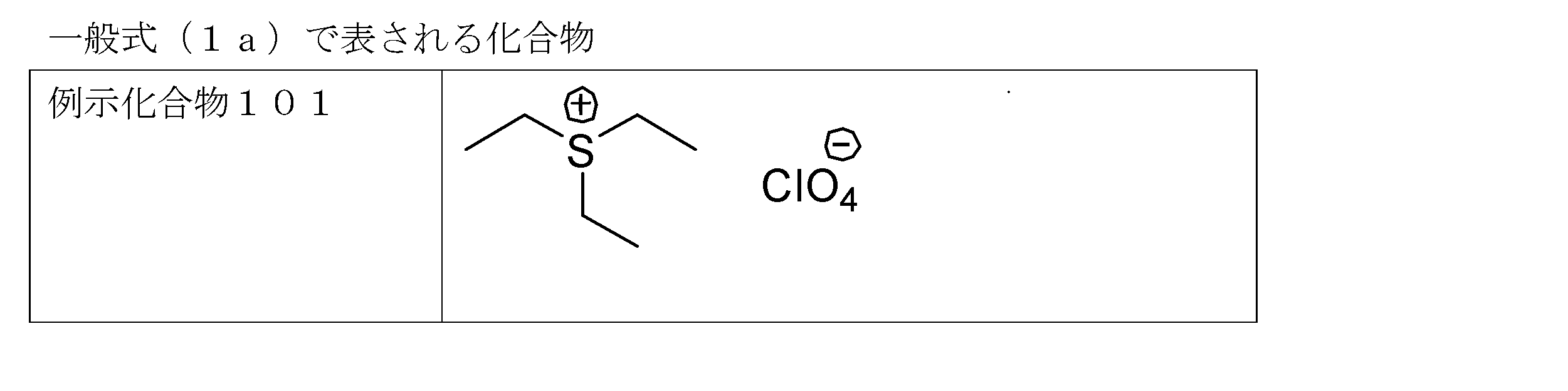
[例示化合物101の合成]
例示化合物101は、文献Journal of Organic Chemistry,1963,vol. 28,p.235-236、に従い合成した。
例示化合物101は、文献Journal of Organic Chemistry,1963,vol. 28,p.235-236、に従い合成した。

[例示化合物201の合成]
例示化合物201は、文献Tetrahedron Letters,2007,vol.48,No.44,p.7774-7777に従い合成した。
例示化合物201は、文献Tetrahedron Letters,2007,vol.48,No.44,p.7774-7777に従い合成した。
[例示化合物202の合成]
例示化合物202は、文献Chemical Communications,2012,vol.48,No.26,p.3185-3187に従い合成した。
例示化合物202は、文献Chemical Communications,2012,vol.48,No.26,p.3185-3187に従い合成した。
[例示化合物203の合成]
例示化合物203は、下記スキームに従い合成した。
化合物A(2.9g)のメタノール溶液(25mL)へ、室温にてトリフルオロメタンスルホン酸(1.6g)を滴下した。さらに40℃にて1時間攪拌した。その後、メタノールを留去し、これにジクロロメタン(50mL)、イオン交換水(20mL)を加え、溶媒抽出し、イオン交換水20mLにて水洗を2回行った。その後、油層を無水硫酸ナトリウムにて乾燥、溶媒留去することで、目的化合物を白色固体として、収率75%で得た。目的化合物は1H-NMRにより同定した。1H-NMRの結果を下記に示す。
1H-NMR(DMSO-d6) 0.75~0.85(m、9H)、1.30~1.40(m、12H)、1.75(d、3H)、2.01~2.11(m、6H)
例示化合物203は、下記スキームに従い合成した。
化合物A(2.9g)のメタノール溶液(25mL)へ、室温にてトリフルオロメタンスルホン酸(1.6g)を滴下した。さらに40℃にて1時間攪拌した。その後、メタノールを留去し、これにジクロロメタン(50mL)、イオン交換水(20mL)を加え、溶媒抽出し、イオン交換水20mLにて水洗を2回行った。その後、油層を無水硫酸ナトリウムにて乾燥、溶媒留去することで、目的化合物を白色固体として、収率75%で得た。目的化合物は1H-NMRにより同定した。1H-NMRの結果を下記に示す。
1H-NMR(DMSO-d6) 0.75~0.85(m、9H)、1.30~1.40(m、12H)、1.75(d、3H)、2.01~2.11(m、6H)

[例示化合物204の合成]
例示化合物204は、文献Journal of the American Chemical Society,1981,vol.103,No.13,p.3959-3961に従い合成した。
例示化合物204は、文献Journal of the American Chemical Society,1981,vol.103,No.13,p.3959-3961に従い合成した。
[例示化合物205の合成]
例示化合物205は、文献Journal of Organic Chemistry,1975,vol.40,p.2801-2806に従い合成した。
例示化合物205は、文献Journal of Organic Chemistry,1975,vol.40,p.2801-2806に従い合成した。
[例示化合物206の合成]
例示化合物206は、文献Journal of the American Chemical Society,1989,vol.111,No.13,p.4766-4776に従い合成した。
例示化合物206は、文献Journal of the American Chemical Society,1989,vol.111,No.13,p.4766-4776に従い合成した。

[例示化合物301の合成]
例示化合物301は、N-ブチルピリジニウム ブロミド(1g)をイオン交換水20mLに溶解させ、この水溶液にリチウム ビス(トリフルオロメタンスルホニル)イミド(1.5g)を加え、室温で1時間攪拌した。これにジクロロメタン(50mL)を加え、溶媒抽出し、イオン交換水20mLにて水洗を2回行った。その後、油層を無水硫酸ナトリウムにて乾燥、溶媒留去して、目的化合物を油状物として、収率90%で得た。目的化合物は1H-NMRにより同定した。1H-NMRの結果を下記に示す。
1H-NMR(DMSO-d6):0.89~0.94(m、3H)1.24~1.37(m、2H)、1.86~1.98(m、2H)、4,58~4.63(t、2H)、8,13~8.17(m、2H)、8,57~8.62(m、1H)、9.07~9.09(m、2H)
例示化合物301は、N-ブチルピリジニウム ブロミド(1g)をイオン交換水20mLに溶解させ、この水溶液にリチウム ビス(トリフルオロメタンスルホニル)イミド(1.5g)を加え、室温で1時間攪拌した。これにジクロロメタン(50mL)を加え、溶媒抽出し、イオン交換水20mLにて水洗を2回行った。その後、油層を無水硫酸ナトリウムにて乾燥、溶媒留去して、目的化合物を油状物として、収率90%で得た。目的化合物は1H-NMRにより同定した。1H-NMRの結果を下記に示す。
1H-NMR(DMSO-d6):0.89~0.94(m、3H)1.24~1.37(m、2H)、1.86~1.98(m、2H)、4,58~4.63(t、2H)、8,13~8.17(m、2H)、8,57~8.62(m、1H)、9.07~9.09(m、2H)
[例示化合物302の合成]
例示化合物302は、例示化合物301の合成において、N-ブチルピリジニウム ブロミドの代わりに、等モル量の1,2-ジメチル-3-ブチルイミダゾール ブロミドを用い、リチウム ビス(トリフルオロメタンスルホニル)イミドの代わりに等モル量のテトラフルオロホウ酸ナトリウムを用いた以外は同様にして、合成した。
例示化合物302は、例示化合物301の合成において、N-ブチルピリジニウム ブロミドの代わりに、等モル量の1,2-ジメチル-3-ブチルイミダゾール ブロミドを用い、リチウム ビス(トリフルオロメタンスルホニル)イミドの代わりに等モル量のテトラフルオロホウ酸ナトリウムを用いた以外は同様にして、合成した。
[例示化合物303の合成]
例示化合物303は、例示化合物301の合成において、N-ブチルピリジニウム ブロミドの代わりに、等モル量の1-ブチル-3-メチルイミダゾール ブロミドを用い、リチウム ビス(トリフルオロメタンスルホニル)イミドの代わりに等モル量のテトラフェニルホウ酸ナトリウムを用いた以外は同様にして、合成した。
例示化合物303は、例示化合物301の合成において、N-ブチルピリジニウム ブロミドの代わりに、等モル量の1-ブチル-3-メチルイミダゾール ブロミドを用い、リチウム ビス(トリフルオロメタンスルホニル)イミドの代わりに等モル量のテトラフェニルホウ酸ナトリウムを用いた以外は同様にして、合成した。
[例示化合物304の合成]
例示化合物304は文献Tetrahedron Letters,1965,1817,1819に従い、合成した。
例示化合物304は文献Tetrahedron Letters,1965,1817,1819に従い、合成した。
[例示化合物305の合成]
例示化合物305は、例示化合物301の合成において、N-ブチルピリジニウム ブロミドの代わりに、等モル量の1-ブチル-1-メチル-ピペリジン ブロミドを用い、リチウム ビス(トリフルオロメタンスルホニル)イミドの代わりに等モル量のテトラフルオロホウ酸ナトリウムを用いた以外は同様にして、合成した。
例示化合物305は、例示化合物301の合成において、N-ブチルピリジニウム ブロミドの代わりに、等モル量の1-ブチル-1-メチル-ピペリジン ブロミドを用い、リチウム ビス(トリフルオロメタンスルホニル)イミドの代わりに等モル量のテトラフルオロホウ酸ナトリウムを用いた以外は同様にして、合成した。
下記に示す共役高分子1~3を用いた。下記繰り返し構造において、*は繰り返し構造の連結部位を表し、Meはメチル基を表す。

共役高分子1~3の分子量は下記のとおりである。
共役高分子1:重量平均分子量=32000
共役高分子2:重量平均分子量=25000
共役高分子3:重量平均分子量=45000
共役高分子1:重量平均分子量=32000
共役高分子2:重量平均分子量=25000
共役高分子3:重量平均分子量=45000
実施例
熱電変換層及び熱電変換素子の作製
表1-2に示す量の例示化合物301、必要により表1-2に示す量の共役高分子、CNT(ASP-100F、Hanwha Nanotech社製)3mgを、オルトジクロロベンゼン4.0ml中に添加し、超音波水浴にて70分間分散させ分散液301を得た。
第一の電極として金(厚み20nm、長さ1cm、幅:1cm)を片側表面に有するポリエチレンテレフタレートフィルム(厚み:125μm)の電極表面に、熱電変換材料として前記分散液301をガラス棒を用いてバー塗布した。80℃にて80分間加熱して溶媒を蒸発させた後、80℃真空下にて8時間乾燥させることにより熱電変換層301(膜厚1.5μm)を形成した。熱電変換層301の上部に、電極が対向するよう第二の電極として金を蒸着したポリエチレンテレフタレートフィルムを80℃にて貼り合わせ、熱電変換素子301を作製した。
熱電変換層及び熱電変換素子の作製
表1-2に示す量の例示化合物301、必要により表1-2に示す量の共役高分子、CNT(ASP-100F、Hanwha Nanotech社製)3mgを、オルトジクロロベンゼン4.0ml中に添加し、超音波水浴にて70分間分散させ分散液301を得た。
第一の電極として金(厚み20nm、長さ1cm、幅:1cm)を片側表面に有するポリエチレンテレフタレートフィルム(厚み:125μm)の電極表面に、熱電変換材料として前記分散液301をガラス棒を用いてバー塗布した。80℃にて80分間加熱して溶媒を蒸発させた後、80℃真空下にて8時間乾燥させることにより熱電変換層301(膜厚1.5μm)を形成した。熱電変換層301の上部に、電極が対向するよう第二の電極として金を蒸着したポリエチレンテレフタレートフィルムを80℃にて貼り合わせ、熱電変換素子301を作製した。
例示化合物を下記表1-1又は表1-2に示すように変更した以外は熱電変換素子301と同様にして、熱電変換層101、201~206、302~305を作製した後、熱電変換素子101、201~206、302~305を作製した。
例示化合物301の添加量を下記表1-2に示すように変更した以外は熱電変換素子301と同様にして、熱電変換層306~309を作製した後、熱電変換素子306~309を作製した。
例示化合物201の添加量を下記表1-1に示すように変更した以外は熱電変換素子201と同様にして、熱電変換層207~210を作製した後、熱電変換素子207~210を作製した。
下記表1-2に示すよう共役高分子を添加した以外は熱電変換素子301と同様にして、熱電変換層310~312を作製した後、熱電変換素子310~312を作製した。
下記表1-1に示すよう共役高分子を添加した以外は熱電変換素子201と同様にして、熱電変換層211~213を作製した後、熱電変換素子211~213を作製した。
例示化合物にかえてポリスチレン(アルドリッチ社製、製品番号430102)を添加した以外は熱電変換素子301と同様にして、比較の熱電変換層c101を作製した後、比較の熱電変換素子c101を作製した。
次いで、例示化合物を添加しないCNTのみからなる比較の熱電変換層c102、及び比較の熱電変換素子c102の作製を試みたが、CNTが分散できず、成膜できなかった。また、下記評価1~3もできなかった。
次いで、例示化合物を添加しないCNTのみからなる比較の熱電変換層c102、及び比較の熱電変換素子c102の作製を試みたが、CNTが分散できず、成膜できなかった。また、下記評価1~3もできなかった。
作製した熱電変換層及び熱電変換素子を、下記の方法により、電極との密着性、熱電特性値(熱起電力S)、熱電性能の光に対する経時安定性を評価した。結果を表1-1及び1-2に示す。
[評価1.電極との密着性の評価]
テープ剥離試験により、熱電変換層と電極との密着性を評価した。
熱電変換層の表面に、熱電変換層表面に気泡が入らないようにスコッチテープを貼り付け、その後、勢い良くテープを剥がす、剥離試験を行った。剥離試験の評価は、下記の5段階とした。剥離面積が少ないほど、電極に対する熱電変換層の密着性に優れると判断できる。
A:剥離なし
B:熱電変換層の面積の20%未満が剥離
C:熱電変換層の面積の20%以上50%未満が剥離
D:熱電変換層の面積の50%以上75%未満が剥離
E:熱電変換層の面積の75%以上が剥離
テープ剥離試験により、熱電変換層と電極との密着性を評価した。
熱電変換層の表面に、熱電変換層表面に気泡が入らないようにスコッチテープを貼り付け、その後、勢い良くテープを剥がす、剥離試験を行った。剥離試験の評価は、下記の5段階とした。剥離面積が少ないほど、電極に対する熱電変換層の密着性に優れると判断できる。
A:剥離なし
B:熱電変換層の面積の20%未満が剥離
C:熱電変換層の面積の20%以上50%未満が剥離
D:熱電変換層の面積の50%以上75%未満が剥離
E:熱電変換層の面積の75%以上が剥離
[評価2.熱電特性値(熱起電力S)の測定]
熱電変換素子の熱起電力Sを測定し、熱電変換性能を評価した。
熱電変換素子の一方の電極を、一定温度に保ったホットプレート上に設置し、他方の電極上に温度制御用のペルチェ素子を設置した。ホットプレートの温度を一定(100℃)に保ちつつ、ペルチェ素子の温度を低下させることにより両電極間に温度差(0Kを超え4K以下の範囲)を付与した。この時、両電極間に発生した熱起電力(μV)を両電極間に生じた特定の温度差(K)で除することにより、単位温度差当たりの熱起電力(μV/K)を算出し、この値を熱電変換素子の熱電特性値とした。算出した熱電特性値は、比較の熱電変換素子c101の熱電特性値を100とし、これに対する相対値として示した。
熱電変換素子の熱起電力Sを測定し、熱電変換性能を評価した。
熱電変換素子の一方の電極を、一定温度に保ったホットプレート上に設置し、他方の電極上に温度制御用のペルチェ素子を設置した。ホットプレートの温度を一定(100℃)に保ちつつ、ペルチェ素子の温度を低下させることにより両電極間に温度差(0Kを超え4K以下の範囲)を付与した。この時、両電極間に発生した熱起電力(μV)を両電極間に生じた特定の温度差(K)で除することにより、単位温度差当たりの熱起電力(μV/K)を算出し、この値を熱電変換素子の熱電特性値とした。算出した熱電特性値は、比較の熱電変換素子c101の熱電特性値を100とし、これに対する相対値として示した。
[評価3.経時安定性の評価]
耐光性試験により、熱電変換性能の光に対する経時安定性を評価した。
熱電変換層に対し、耐光性試験装置(スーパーキセノンウェザーメーターSX120型(ロングライフキセノンランプ)、スガ試験機(株)製)を用い、放射照度100±25W/m2(波長310nm~400nm)、試験槽内温度35±5℃、ブラックパネル温度50±5℃、相対湿度65±15%の条件で、JIS K 5600-7-5に準じて耐光性試験25時間を実施した。その後、熱電変換層の上部に、電極が対向するよう第二の電極として金を蒸着したポリエチレンテレフタレートフィルムを80℃にて貼り合わせ、熱電変換素子を作製した。熱電変換素子の熱電特性値を、上記評価2.と同様に測定した。得られた値を、対応する上記評価2.の熱電特性値と比較して、下記の5段階で評価した。熱電特性値の変化率が小さいほど、耐光性に優れ、光に対する経時安定性の高い素子と判断できる。
A:熱電特性値の変化率10%未満
B:熱電特性値の変化率10%以上25%未満
C:熱電特性値の変化率25%以上50%未満
D:熱電特性値の変化率50%以上75%未満
E:熱電特性値の変化率75%以上
耐光性試験により、熱電変換性能の光に対する経時安定性を評価した。
熱電変換層に対し、耐光性試験装置(スーパーキセノンウェザーメーターSX120型(ロングライフキセノンランプ)、スガ試験機(株)製)を用い、放射照度100±25W/m2(波長310nm~400nm)、試験槽内温度35±5℃、ブラックパネル温度50±5℃、相対湿度65±15%の条件で、JIS K 5600-7-5に準じて耐光性試験25時間を実施した。その後、熱電変換層の上部に、電極が対向するよう第二の電極として金を蒸着したポリエチレンテレフタレートフィルムを80℃にて貼り合わせ、熱電変換素子を作製した。熱電変換素子の熱電特性値を、上記評価2.と同様に測定した。得られた値を、対応する上記評価2.の熱電特性値と比較して、下記の5段階で評価した。熱電特性値の変化率が小さいほど、耐光性に優れ、光に対する経時安定性の高い素子と判断できる。
A:熱電特性値の変化率10%未満
B:熱電特性値の変化率10%以上25%未満
C:熱電特性値の変化率25%以上50%未満
D:熱電特性値の変化率50%以上75%未満
E:熱電特性値の変化率75%以上
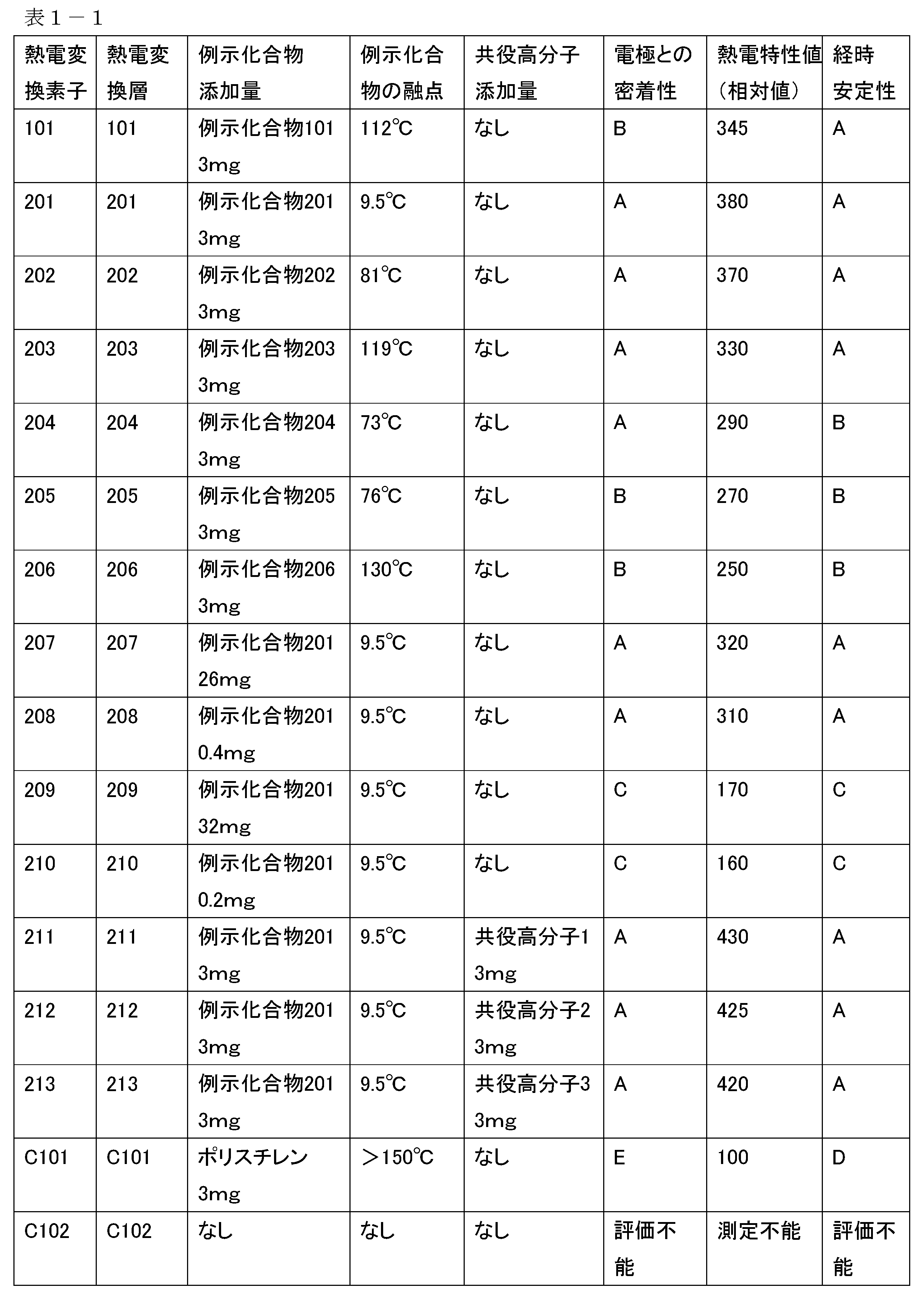
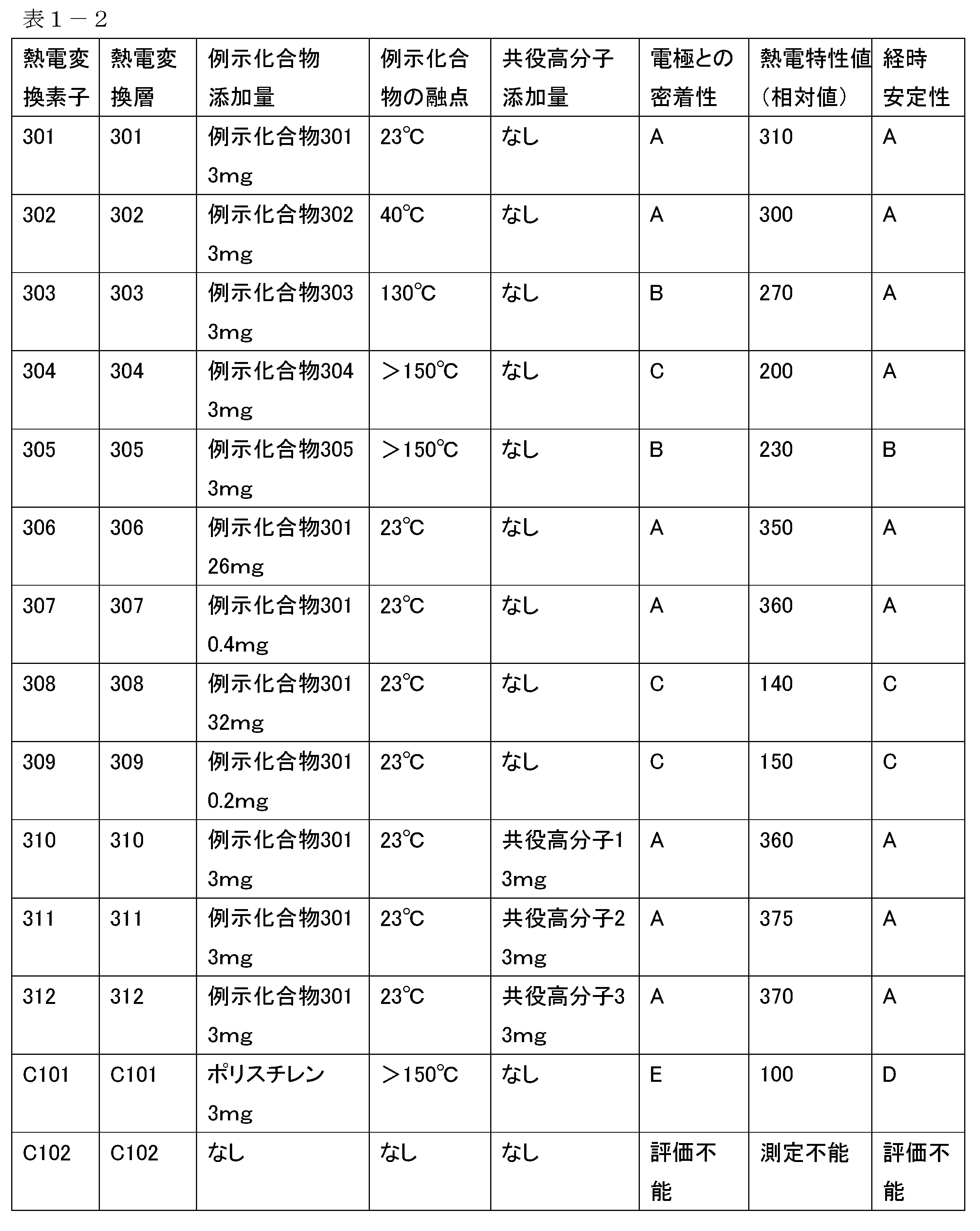
表1-1及び1-2から明らかなように、前記一般式(1a)~(3b)で表される例示化合物101、201~206、301~305を用いた熱電変換素子101、201~206、301~312は、ポリスチレンを用いた比較素子c101と比べ、電極と熱電変換層との密着性に優れ、高い熱電特性値を示した。
さらに、熱電変換素子101、201~206、301~312は、経時安定性にも優れていた。特に、カチオン部にアルキル基を有する例示化合物101、201~203、カチオン部に含窒素芳香族へテロ環基を有する化合物である例示化合物301~304を用いた素子101、201~203、301~304は、特に優れた経時安定性を示した。
また、熱電変換素子207~210、306~309の結果から、熱電変換層における例示化合物とCNTとの含有比率を1:9~9:1の範囲内とすることで、熱電変換層との密着性、熱電特性値、経時安定性がより一層向上することがわかった。
また、例示化合物とCNTに加えて、共役高分子を添加した熱電変換素子211~213、310~312は、高い熱電特性値を示した。
一方、ポリスチレンを用いた比較素子c101は、電極と熱電変換層との密着性が非常に悪く、熱電特性値、経時安定性においても、本発明の熱電変換素子より大幅に劣っていた。
さらに、熱電変換素子101、201~206、301~312は、経時安定性にも優れていた。特に、カチオン部にアルキル基を有する例示化合物101、201~203、カチオン部に含窒素芳香族へテロ環基を有する化合物である例示化合物301~304を用いた素子101、201~203、301~304は、特に優れた経時安定性を示した。
また、熱電変換素子207~210、306~309の結果から、熱電変換層における例示化合物とCNTとの含有比率を1:9~9:1の範囲内とすることで、熱電変換層との密着性、熱電特性値、経時安定性がより一層向上することがわかった。
また、例示化合物とCNTに加えて、共役高分子を添加した熱電変換素子211~213、310~312は、高い熱電特性値を示した。
一方、ポリスチレンを用いた比較素子c101は、電極と熱電変換層との密着性が非常に悪く、熱電特性値、経時安定性においても、本発明の熱電変換素子より大幅に劣っていた。
本発明をその実施態様とともに説明したが、我々は特に指定しない限り我々の発明を説明のどの細部においても限定しようとするものではなく、添付の請求の範囲に示した発明の精神と範囲に反することなく幅広く解釈されるべきであると考える。
本願は、2013年5月2日に日本国で特許出願された特願2013-96771に基づく優先権を主張するものであり、これはここに参照してその内容を本明細書の記載の一部として取り込む。
1、2 熱電変換素子
11、17 金属板
12、22 第1の基材
13、23 第1の電極
14、24 熱電変換層
15、25 第2の電極
16、26 第2の基材
11、17 金属板
12、22 第1の基材
13、23 第1の電極
14、24 熱電変換層
15、25 第2の電極
16、26 第2の基材
Claims (15)
- 基材上に、第1の電極、熱電変換層及び第2の電極を有する熱電変換素子であって、該熱電変換層に、ナノ導電性材料、及び下記一般式(1a)~(3b)で表される化合物から選択される少なくとも1種の化合物を含有する熱電変換素子。

一般式(1b)中、nは2又は3の整数を表す。Xp-はp価の対アニオンを表し、pは1~3の整数を表す。kは1~3の整数を表す。但し、n=kpである。Lはn価の連結基又は単結合を表す。R12及びR13は、一般式(1a)と同義である。複数のR12及びR13は、同じであっても異なってもよい。
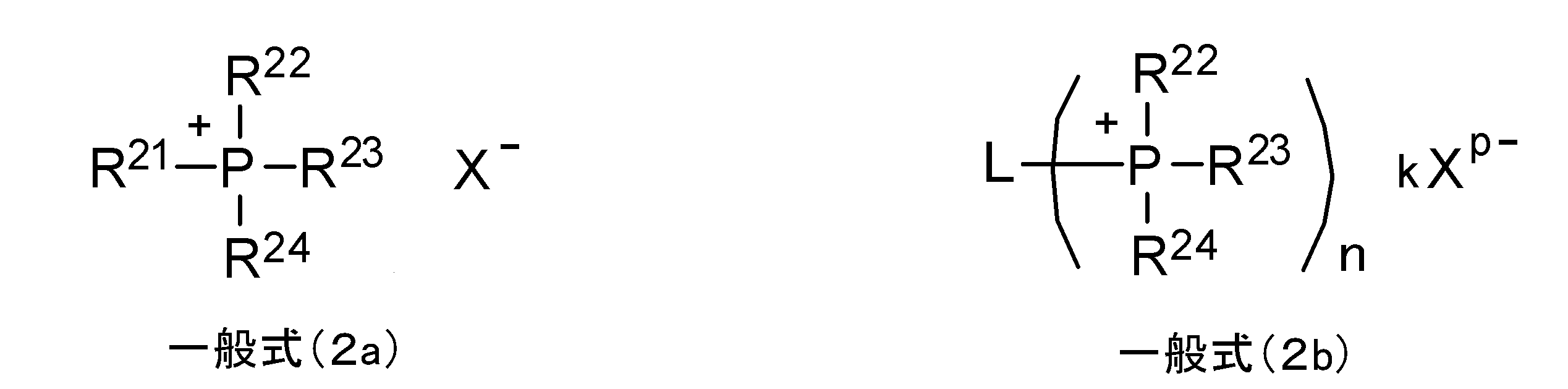
一般式(2b)中、nは2又は3の整数を表す。Xp-はp価の対アニオンを表し、pは1~3の整数を表す。kは1~3の整数を表す。但し、n=kpである。Lはn価の連結基又は単結合を表す。R22~R24は、一般式(2a)と同義である。複数のR22~R24は、同じであっても異なってもよい。
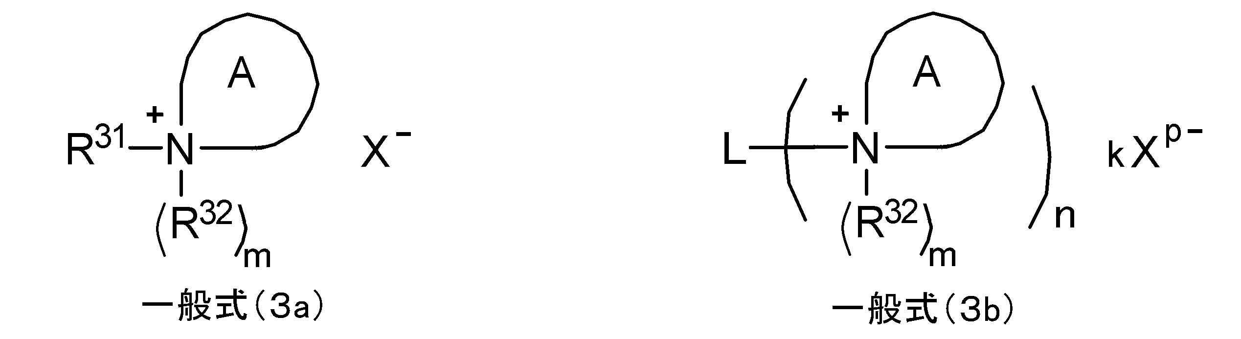
一般式(3b)中、nは2又は3の整数を表す。Xp-はp価の対アニオンを表し、pは1~3の整数を表す。kは1~3の整数を表す。但し、n=kpである。Lはn価の連結基又は単結合を表す。A、R32、mは、一般式(3a)と同義である。複数のA、R32は、同じであっても異なってもよい。 - 一般式(1a)及び(1b)において、R11~R13がアルキル基である、請求項1記載の熱電変換素子。
- 一般式(2a)及び(2b)において、R21~R24がアルキル基である、請求項1記載の熱電変換素子。
- 一般式(3a)及び(3b)において、Aが含窒素芳香族ヘテロ環基である、請求項1記載の熱電変換素子。
- 一般式(1a)~(3b)において、X-又はXp-が強酸の共役塩基である、請求項1~4のいずれか1項に記載の熱電変換素子。
- 一般式(1a)~(3b)で表される化合物の融点が100℃以下である、請求項1~5のいずれか1項に記載の熱電変換素子。
- 熱電変換層におけるナノ導電性材料と一般式(1a)~(3b)で表される化合物との含有比率が、質量基準で1:9~9:1である、請求項1~6のいずれか1項に記載の熱電変換素子。
- ナノ導電性材料が、カーボンナノチューブである、請求項1~7のいずれか1項に記載の熱電変換素子。
- 第1の電極及び第2の電極が、各々独立に、アルミニウム、金、銀又は銅で形成されてなる、請求項1~8のいずれか1項に記載に記載の熱電変換素子。
- 熱電変換層に共役高分子を含む、請求項1~9のいずれか1項に記載の熱電変換素子。
- 請求項1~10のいずれか1項に記載の熱電変換素子を用いた熱電発電用物品。
- 請求項1~10のいずれか1項に記載の熱電変換素子を用いたセンサー用電源。
- ナノ導電性材料及び下記一般式(1a)~(3b)の化合物から選択される少なくとも1種の化合物を含有する、熱電変換素子の熱電変換層を形成するための熱電変換材料。
- 有機溶媒を含む請求項13記載の熱電変換材料。
- ナノ導電性材料を有機溶媒中に分散してなる請求項14記載の熱電変換材料。
Applications Claiming Priority (2)
| Application Number | Priority Date | Filing Date | Title |
|---|---|---|---|
| JP2013-096711 | 2013-05-02 | ||
| JP2013096711A JP2014220286A (ja) | 2013-05-02 | 2013-05-02 | 熱電変換素子 |
Publications (1)
| Publication Number | Publication Date |
|---|---|
| WO2014178284A1 true WO2014178284A1 (ja) | 2014-11-06 |
Family
ID=51843418
Family Applications (1)
| Application Number | Title | Priority Date | Filing Date |
|---|---|---|---|
| PCT/JP2014/060844 Ceased WO2014178284A1 (ja) | 2013-05-02 | 2014-04-16 | 熱電変換材料、熱電変換素子、熱電発電用物品及びセンサー用電源 |
Country Status (2)
| Country | Link |
|---|---|
| JP (1) | JP2014220286A (ja) |
| WO (1) | WO2014178284A1 (ja) |
Cited By (3)
| Publication number | Priority date | Publication date | Assignee | Title |
|---|---|---|---|---|
| CN112106211A (zh) * | 2018-04-27 | 2020-12-18 | 国立研究开发法人科学技术振兴机构 | 热电转换元件 |
| JPWO2021235526A1 (ja) * | 2020-05-21 | 2021-11-25 | ||
| WO2023063177A1 (ja) * | 2021-10-12 | 2023-04-20 | デンカ株式会社 | 熱電変換素子及びその製造方法 |
Families Citing this family (3)
| Publication number | Priority date | Publication date | Assignee | Title |
|---|---|---|---|---|
| JP6845521B1 (ja) * | 2020-09-30 | 2021-03-17 | 株式会社Gceインスティチュート | 発電素子、発電装置、電子機器、及び発電素子の製造方法 |
| JP7011361B1 (ja) | 2021-09-10 | 2022-01-26 | 株式会社Gceインスティチュート | 発電素子の製造方法、発電素子、発電装置、及び電子機器 |
| JP2023062767A (ja) * | 2021-10-22 | 2023-05-09 | 東洋インキScホールディングス株式会社 | 熱電変換材料および熱電変換素子 |
Citations (5)
| Publication number | Priority date | Publication date | Assignee | Title |
|---|---|---|---|---|
| JP2003046145A (ja) * | 2001-04-27 | 2003-02-14 | Naoki Toshima | 熱電材料及び熱電素子並びに熱電材料の製造方法 |
| JP2005220316A (ja) * | 2004-02-09 | 2005-08-18 | Tokai Rubber Ind Ltd | 電子写真機器用導電性組成物およびその製法、ならびにそれを用いた電子写真機器用導電性部材 |
| JP2009035619A (ja) * | 2007-08-01 | 2009-02-19 | Konica Minolta Holdings Inc | 導電性組成物及び導電性膜 |
| JP2011250676A (ja) * | 2010-04-27 | 2011-12-08 | Canon Inc | アクチュエータ |
| WO2012133314A1 (ja) * | 2011-03-28 | 2012-10-04 | 富士フイルム株式会社 | 導電性組成物、当該組成物を用いた導電性膜及びその製造方法 |
-
2013
- 2013-05-02 JP JP2013096711A patent/JP2014220286A/ja active Pending
-
2014
- 2014-04-16 WO PCT/JP2014/060844 patent/WO2014178284A1/ja not_active Ceased
Patent Citations (5)
| Publication number | Priority date | Publication date | Assignee | Title |
|---|---|---|---|---|
| JP2003046145A (ja) * | 2001-04-27 | 2003-02-14 | Naoki Toshima | 熱電材料及び熱電素子並びに熱電材料の製造方法 |
| JP2005220316A (ja) * | 2004-02-09 | 2005-08-18 | Tokai Rubber Ind Ltd | 電子写真機器用導電性組成物およびその製法、ならびにそれを用いた電子写真機器用導電性部材 |
| JP2009035619A (ja) * | 2007-08-01 | 2009-02-19 | Konica Minolta Holdings Inc | 導電性組成物及び導電性膜 |
| JP2011250676A (ja) * | 2010-04-27 | 2011-12-08 | Canon Inc | アクチュエータ |
| WO2012133314A1 (ja) * | 2011-03-28 | 2012-10-04 | 富士フイルム株式会社 | 導電性組成物、当該組成物を用いた導電性膜及びその製造方法 |
Cited By (8)
| Publication number | Priority date | Publication date | Assignee | Title |
|---|---|---|---|---|
| CN112106211A (zh) * | 2018-04-27 | 2020-12-18 | 国立研究开发法人科学技术振兴机构 | 热电转换元件 |
| CN112106211B (zh) * | 2018-04-27 | 2024-03-26 | 国立研究开发法人科学技术振兴机构 | 热电转换元件 |
| JPWO2021235526A1 (ja) * | 2020-05-21 | 2021-11-25 | ||
| JP7692904B2 (ja) | 2020-05-21 | 2025-06-16 | デンカ株式会社 | 熱電変換用n型材料及びその製造方法、ドーパント並びに熱電変換素子 |
| WO2023063177A1 (ja) * | 2021-10-12 | 2023-04-20 | デンカ株式会社 | 熱電変換素子及びその製造方法 |
| JPWO2023063177A1 (ja) * | 2021-10-12 | 2023-04-20 | ||
| EP4391780A4 (en) * | 2021-10-12 | 2024-11-27 | Denka Company Limited | THERMOELECTRIC CONVERTER ELEMENT AND METHOD FOR ITS PRODUCTION |
| JP7693822B2 (ja) | 2021-10-12 | 2025-06-17 | デンカ株式会社 | 熱電変換素子及びその製造方法 |
Also Published As
| Publication number | Publication date |
|---|---|
| JP2014220286A (ja) | 2014-11-20 |
Similar Documents
| Publication | Publication Date | Title |
|---|---|---|
| JP5789580B2 (ja) | 熱電変換材料及び熱電変換素子 | |
| JP5960178B2 (ja) | 熱電変換素子の製造方法および熱電変換層用分散物の製造方法 | |
| JP5848284B2 (ja) | 熱電変換素子及びこれを用いた熱電変換材料 | |
| JP6110818B2 (ja) | 熱電変換材料、熱電変換素子ならびにこれを用いた熱電発電用物品およびセンサー用電源 | |
| JP5951539B2 (ja) | 熱電変換材料、熱電変換素子ならびにこれを用いた熱電発電用物品およびセンサー用電源 | |
| WO2014178284A1 (ja) | 熱電変換材料、熱電変換素子、熱電発電用物品及びセンサー用電源 | |
| JP5931807B2 (ja) | 熱電変換材料、これを用いた熱電変換素子及び熱電発電用物品、並びに熱電変換素子の製造方法 | |
| JP6744406B2 (ja) | n型半導体層、熱電変換層、熱電変換素子、熱電変換モジュール、及びn型半導体層形成用組成物 | |
| JP5931764B2 (ja) | 熱電変換材料、熱電変換素子並びにこれを用いた熱電発電用物品及びセンサー用電源 | |
| JP6771844B2 (ja) | 熱電変換層、熱電変換層形成用組成物、熱電変換素子、熱電変換モジュール | |
| WO2014119468A1 (ja) | 熱電変換材料、熱電変換素子並びにこれを用いた熱電発電用物品及びセンサー用電源 | |
| JP6698565B2 (ja) | 熱電変換層、熱電変換素子、熱電変換モジュール | |
| JP6009422B2 (ja) | 熱電変換材料、熱電変換素子、及び熱電変換素子の製造方法 | |
| JP6761473B2 (ja) | 熱電変換素子 | |
| JP5931762B2 (ja) | 熱電変換材料、熱電変換素子並びにこれを用いた熱電発電用物品及びセンサー用電源 | |
| JP5931763B2 (ja) | 熱電変換材料、熱電変換素子並びにこれを用いた熱電発電用物品及びセンサー用電源 | |
| JP6670382B2 (ja) | p型半導体層、熱電変換層、熱電変換素子、熱電変換モジュール、及びp型半導体層形成用組成物 | |
| JPWO2017104591A1 (ja) | n型熱電変換層、熱電変換素子およびn型熱電変換層形成用組成物 |
Legal Events
| Date | Code | Title | Description |
|---|---|---|---|
| 121 | Ep: the epo has been informed by wipo that ep was designated in this application |
Ref document number: 14791634 Country of ref document: EP Kind code of ref document: A1 |
|
| NENP | Non-entry into the national phase |
Ref country code: DE |
|
| 122 | Ep: pct application non-entry in european phase |
Ref document number: 14791634 Country of ref document: EP Kind code of ref document: A1 |