WO2014174716A1 - 電界効果型半導体装置及びその製造方法 - Google Patents
電界効果型半導体装置及びその製造方法 Download PDFInfo
- Publication number
- WO2014174716A1 WO2014174716A1 PCT/JP2013/081938 JP2013081938W WO2014174716A1 WO 2014174716 A1 WO2014174716 A1 WO 2014174716A1 JP 2013081938 W JP2013081938 W JP 2013081938W WO 2014174716 A1 WO2014174716 A1 WO 2014174716A1
- Authority
- WO
- WIPO (PCT)
- Prior art keywords
- semiconductor substrate
- source
- drain electrode
- insulating film
- electrode
- Prior art date
- Legal status (The legal status is an assumption and is not a legal conclusion. Google has not performed a legal analysis and makes no representation as to the accuracy of the status listed.)
- Ceased
Links
Images






Classifications
-
- H—ELECTRICITY
- H10—SEMICONDUCTOR DEVICES; ELECTRIC SOLID-STATE DEVICES NOT OTHERWISE PROVIDED FOR
- H10D—INORGANIC ELECTRIC SEMICONDUCTOR DEVICES
- H10D64/00—Electrodes of devices having potential barriers
- H10D64/01—Manufacture or treatment
- H10D64/013—Manufacture or treatment of electrodes having a conductor capacitively coupled to a semiconductor by an insulator
- H10D64/01358—Manufacture or treatment of electrodes having a conductor capacitively coupled to a semiconductor by an insulator the insulator being formed after the semiconductor body, the semiconductor being a Group III-V material
-
- H—ELECTRICITY
- H10—SEMICONDUCTOR DEVICES; ELECTRIC SOLID-STATE DEVICES NOT OTHERWISE PROVIDED FOR
- H10D—INORGANIC ELECTRIC SEMICONDUCTOR DEVICES
- H10D30/00—Field-effect transistors [FET]
- H10D30/01—Manufacture or treatment
- H10D30/021—Manufacture or treatment of FETs having insulated gates [IGFET]
-
- H—ELECTRICITY
- H10—SEMICONDUCTOR DEVICES; ELECTRIC SOLID-STATE DEVICES NOT OTHERWISE PROVIDED FOR
- H10D—INORGANIC ELECTRIC SEMICONDUCTOR DEVICES
- H10D30/00—Field-effect transistors [FET]
- H10D30/60—Insulated-gate field-effect transistors [IGFET]
-
- H—ELECTRICITY
- H10—SEMICONDUCTOR DEVICES; ELECTRIC SOLID-STATE DEVICES NOT OTHERWISE PROVIDED FOR
- H10D—INORGANIC ELECTRIC SEMICONDUCTOR DEVICES
- H10D62/00—Semiconductor bodies, or regions thereof, of devices having potential barriers
- H10D62/80—Semiconductor bodies, or regions thereof, of devices having potential barriers characterised by the materials
- H10D62/85—Semiconductor bodies, or regions thereof, of devices having potential barriers characterised by the materials being Group III-V materials, e.g. GaAs
-
- H—ELECTRICITY
- H10—SEMICONDUCTOR DEVICES; ELECTRIC SOLID-STATE DEVICES NOT OTHERWISE PROVIDED FOR
- H10D—INORGANIC ELECTRIC SEMICONDUCTOR DEVICES
- H10D64/00—Electrodes of devices having potential barriers
- H10D64/60—Electrodes characterised by their materials
- H10D64/66—Electrodes having a conductor capacitively coupled to a semiconductor by an insulator, e.g. MIS electrodes
- H10D64/667—Electrodes having a conductor capacitively coupled to a semiconductor by an insulator, e.g. MIS electrodes the conductor comprising a layer of alloy material, compound material or organic material contacting the insulator, e.g. TiN workfunction layers
Definitions
- Embodiments described herein relate generally to a field effect semiconductor device having a metal S / D structure and a method for manufacturing the same.
- a so-called metal S / D structure in which a source / drain (S / D) metal electrode is adjacent to a channel region has been proposed as a structure that can be expected to have advantages such as reduction of parasitic resistance and simplification of a device fabrication process.
- a process has been developed in which Ni—InGaAs, which is an alloy of Ni and InGaAs, is formed on the source / drain (S / D) electrodes in a self-aligned manner, and a metal S / D InGaAs-nMOSFET using the process is developed.
- Ni—InGaAs which is an alloy of Ni and InGaAs
- the thickness of the S / D electrode layer is preferable to reduce the thickness of the S / D electrode layer to about 1/3 of the gate length from the viewpoint of suppressing the short channel effect.
- an ultra-thin Ni—InGaAs alloy layer having a film thickness of 10 nm or less can be formed by controlling the Ni deposition amount and the heat treatment temperature (Patent Document 1, Non-Patent Document). 2).
- a metal S / D InGaAs-nMOSFET having an ultrathin Ni—InGaAs S / D electrode can be fabricated.
- the contact hole reaches the InGaAs alloy layer and at the same time the RIE for forming the contact hole is completed, the InGaAs alloy layer is not over-etched, but in order to secure a process margin on the entire wafer surface. This over-etching is inevitable.
- the disappearance of the InGaAs alloy layer under the plug is considered to cause problems such as an increase in junction leakage and an increase in resistance due to a reduction in contact area. Therefore, the alloy layer under the plug remains even after a sufficient process margin is secured. It is hoped that
- the problem to be solved by the present invention is to realize a reliable connection between a contact plug and a metal source / drain electrode while ensuring a process margin of RIE for forming a contact hole. It is an object to provide a field effect semiconductor device capable of suppressing the increase and a manufacturing method thereof.
- a field effect semiconductor device is formed on a surface portion of a semiconductor substrate, a gate electrode provided on the semiconductor substrate via a gate insulating film, and a channel region under the gate electrode.
- a source / drain electrode made of an alloy of a metal and a semiconductor constituting the semiconductor substrate, and a contact plug in contact with the source / drain electrode, and the source / drain electrode in a region immediately below the contact plug And the semiconductor substrate are present at a deeper position on the semiconductor substrate side than the interface between the source / drain electrodes in the other regions and the semiconductor substrate.
- the method of manufacturing a field effect semiconductor device includes a step of forming a gate electrode on a semiconductor substrate through a gate insulating film, and a surface region of the semiconductor substrate with a channel region under the gate electrode interposed therebetween. Forming a first source / drain electrode made of an alloy of a metal and a semiconductor of the semiconductor substrate, and forming an interlayer insulating film so as to cover the gate electrode and the first source / drain electrode.
- a contact hole connected to the first source / drain electrode in the interlayer insulating film, and forming a metal and the semiconductor substrate in a surface portion of the semiconductor substrate at a bottom of the contact hole A second source / drain electrode formed of an alloy with a semiconductor and formed deeper in the semiconductor substrate than the first source / drain electrode. A and forming, in the contact hole, forming a contact plug to contact the second source / drain electrode.
- the interface between the metal S / D electrode immediately below the contact plug and the semiconductor substrate is located deeper on the semiconductor substrate side than the interface between the S / D electrode and the semiconductor substrate in other regions. , S / D electrodes are formed. Therefore, even if overetching for forming the contact hole occurs, the contact plug and the metal S / D electrode are reliably connected. Thereby, a sufficient process margin can be ensured in the RIE for forming the contact hole without causing problems such as junction leakage and an increase in resistance.
- FIG. 1 is a sectional view showing a schematic structure of an InGaAs-MOSFET according to the first embodiment.
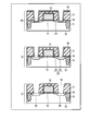
- FIG. 2 is a cross-sectional view showing a manufacturing process of the InGaAs-MOSFET of the first embodiment.
- FIG. 3 is a cross-sectional view showing a manufacturing process of the InGaAs-MOSFET of the first embodiment.
- FIG. 4 is a cross-sectional view showing a manufacturing process of the InGaAs-MOSFET of the first embodiment.
- FIG. 5 is a cross-sectional view showing a schematic structure of an InGaAs-MOSFET according to the second embodiment.
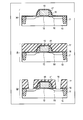
- FIG. 6 is a cross-sectional view showing a manufacturing process of the InGaAs-MOSFET of the second embodiment.
- FIG. 7 is a cross-sectional view showing a manufacturing process of the InGaAs-MOSFET of the second embodiment.
- FIG. 8 is a cross-sectional view showing a schematic structure of an InGaAs-MOSFET according to the third embodiment.
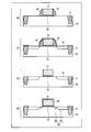
- FIG. 9 is a cross-sectional view showing a manufacturing process of the InGaAs-MOSFET of the third embodiment.
- FIG. 10 is a cross-sectional view showing a manufacturing process of the InGaAs-MOSFET of the third embodiment.
- FIG. 1 is a sectional view showing a schematic structure of an InGaAs-MOSFET according to the first embodiment.
- a gate electrode 13 is formed on an In x Ga 1-x As substrate (semiconductor substrate) 10 via a gate insulating film 12, and is formed on the surface portion of the substrate 10 with the gate electrode 13 interposed therebetween.
- a source electrode and a drain electrode (hereinafter referred to as source / drain electrodes or S / D electrodes) 20 made of metal electrodes are formed. That is, the MOSFET of this embodiment has a so-called metal S / D structure in which a metal electrode such as Ni—InGaAs is adjacent to the channel as the S / D electrode 20.
- Al 2 O 3, HfO 2 , La 2 O 3 or a mixture thereof can be used.
- a material of the gate electrode 13 used Ta, TaN, Ti, TiN, Ni, Au, various metals or NiSix and NiGex such an alloy such as Pt, also a poly-Si 1-x Ge x or the like which has been subjected to heavy doping be able to.
- the gate stack structure and materials there are no restrictions on the gate stack structure and materials.
- the material of the S / D electrode 20 it is possible to use an alloy containing Co, Pt, etc. in addition to Ni.
- An interlayer insulating film 17 is provided on the substrate 10 on which the gate insulating film 12 and the gate electrode 13 are formed.
- a contact hole is formed in the interlayer insulating film 17 and the contact plug 30 is buried in the contact hole, whereby the contact plug 30 is connected to the S / D electrode 20.
- the portion (second S / D electrode) 22 immediately below the plug of the S / D electrode 20 is deeper than the peripheral portion (first S / D electrode) 21 immediately below the plug of the S / D electrode 20. To the position. That is, the interface between the second S / D electrode 22 and the semiconductor substrate 10 immediately below the plug is located deeper on the semiconductor substrate side than the interface between the first S / D electrode 21 and the semiconductor substrate 10 in the peripheral portion. Existing.
- the plug 30 includes a barrier metal 31 such as Ti or TiN, and a conductive film 32 made of W, Pd, Al, Cu, Au, or an alloy thereof. There are no restrictions on the structure and material of the plug, and the use of the barrier metal 31 is not essential.
- an element isolation embedded insulating film 11 is formed so as to surround an element formation region in an In x Ga 1-x As substrate 10, and then, via a gate insulating film 12.
- the gate electrode 13 is formed.
- an In x Ga 1-x As substrate 10 an In x Ga 1-x As layer is formed by epitaxial growth on a compound semiconductor substrate such as InP or GaAs or on a Si or Ge substrate.
- the In x Ga 1-x As layer can be formed by bonding to various base substrates.
- a metal film 14 containing Ni is deposited to form an S / D electrode.
- a gate sidewall insulating film may be formed on the side surface of the gate electrode 13 with SiO 2 , SiN, or the like.
- the thickness of the deposited metal film 14 is preferably 30 nm or less, but more preferably 10 nm or less.
- the film thickness of the alloy is preferably about 10 nm or less from the viewpoint of resistance to the short channel effect, and for this purpose, the amount of deposited metal is 10 nm. This is because it is preferable to limit to the following.
- a first S / D electrode made of an alloy of the above metal and InGaAs and having a thickness of 10 nm or less is obtained by performing heat treatment and alloying treatment. 21 is formed.
- the temperature of the heat treatment for alloying is desirably 200 to 350 ° C. This is because the alloying reaction hardly occurs at a temperature lower than this temperature range, and the alloy layer becomes thick at a high temperature.
- etching of the metal film 14 that connects the gate electrode 13 and the S / D electrode 21 is performed.
- Ni is deposited, it is possible to perform etching while maintaining a selection ratio between the material of the gate electrode 13 and the S / D electrode 21 of Ni—InGaAs with HCl. Thereby, electrical separation between the gate electrode 13 and the S / D electrode 21 is performed.
- an insulating film 16 serving as an etching stopper for contact hole etching such as SiN is deposited.
- an interlayer insulating film 17 such as SiO 2 is deposited.
- the film thickness of these films 17 is arbitrary and may be set according to the application.
- CMP chemical mechanical polishing
- contact holes 18 are formed on the interlayer insulating film 17 and the stopper insulating film 16 by using RIE.
- RIE reactive ion etching
- the underlying S / D electrode 21 is over-etched, and in some cases, as shown in FIG. 3G, the alloy layer 21 becomes extremely thin or all of the alloy layer 21 is etched. Is assumed. If the contact plug is formed in a state where the alloy layer 21 has disappeared, there is a possibility that problems such as an increase in leakage current and an increase in resistance due to a reduction in contact area may be caused. Therefore, in this embodiment, the alloy layer is re-formed after the contact hole is formed.
- a metal film 19 such as Ni is deposited as shown in FIG. Although it is desirable to deposit the same metal as that previously used for forming the S / D electrode, the metal species of the deposited metal may be changed.
- the thickness of the deposited metal film 19 is desirably 30 nm or less.
- a heat treatment is performed at 200 to 350 ° C. to thereby form the alloy layer 22, that is, the second S / D electrode. 22 is formed.
- the S / D electrode 22 is formed in the contact hole portion to a position deeper than the surrounding region 21. That is, as the metal S / D electrode 20, S / D electrodes 21 and 22 having different film thicknesses are formed in the region 22 immediately below the contact plug (contact hole) and the other region 21.
- the unreacted metal film 19 is selectively etched with HCl or the like. Thereafter, the barrier metal 31 and the plug metal 32 are deposited to form the contact plug 30, whereby the structure shown in FIG. 1 is obtained. Thereafter, a wiring process according to the Si-LSI process can be performed.
- Ni is deposited again. And the heat treatment are performed, a Ni—InGaAs alloy layer 22 is newly formed immediately below the contact hole 18.
- the contact plug 30 and the Ni—InGaAs layer (S / D electrode) 20 are securely connected, and a sufficient process margin is achieved in the RIE for forming the contact hole without causing problems such as junction leakage and increased resistance. Can be secured.
- the MOSFET of the present embodiment can suppress junction leakage and increase in resistance. This is effective for realizing a CMOS-LSI with high performance and low power consumption.
- FIG. 5 is a cross-sectional view showing a schematic structure of an InGaAs-MOSFET according to the second embodiment.
- symbol is attached
- the difference between the present embodiment and the first embodiment described above is that the metal S / D electrode is not formed after the contact hole is formed, but the metal S / D electrode is formed thick in advance in a region other than the vicinity of the gate. It is to be done.
- gate sidewall insulating films 41 are formed on both sides of the gate electrode 13.
- the thickness of the S / D electrode 50 is thin at the portion (first S / D electrode) 51 below the gate sidewall insulating film 41 and thick at the portion outside it (second S / D electrode) 52. ing. That is, the thickness of the S / D electrode 50 is thick at the contact portion between the S / D electrode 50 and the contact plug 31, and the thickness of the S / D electrode 50 is thin near the gate.
- the contact hole does not penetrate the S / D electrode 20 due to the formation of the contact hole.
- the S / D electrode 50 can be made sufficiently thin in the vicinity of the gate.
- a gate insulating film 12 and a gate are formed.
- An electrode 13 is formed on the substrate 10.
- a thin first S / D electrode 51 is formed in a region of the substrate 10 excluding the gate portion (channel region).
- a Ni film deposition process, a heat treatment process, and an unreacted Ni film removal process may be performed as in the first embodiment.
- a gate sidewall insulating film 41 is formed.
- the gate sidewall insulating film 41 is formed by, for example, depositing a silicon oxide film on the entire surface and then etching back the silicon oxide film so that the oxide film 41 remains on the sidewall of the gate electrode 13. It only has to be executed.
- a metal film 42 containing Ni is deposited for the formation of the S / D electrode.
- the thickness of the deposited metal film 42 is desirably 30 nm or less, for example, 20 nm.
- the metal film is thicker than the first embodiment because the alloyed region is a region excluding the vicinity of the gate, and it is not necessary to limit the film thickness of the alloy layer to about 10 nm or less. .
- a second S / D electrode 52 made of an alloy of the above metal and InGaAs is formed by performing a heat treatment and an alloying treatment.
- the metal S / D electrode 50 S / D electrodes 51 and 52 having different film thicknesses are formed in a region immediately below the gate sidewall insulating film 41 and other regions.
- the temperature of the heat treatment for alloying is desirably 200 to 350 ° C. The reason why the heat treatment is performed in this temperature range is that the alloying reaction is unlikely to occur at low temperatures and the alloy layer becomes thick at high temperatures.
- etching of the metal film 42 that connects the gate electrode 13 and the S / D electrode 50 is performed.
- Ni is deposited as the metal film 42, it is possible to etch the metal film 42 while ensuring a selective ratio between the metal film 42 and the Ni / InGaAs S / D electrode 50 with HCl. Thereby, electrical separation between the gate electrode 13 and the S / D electrode 50 is performed.
- an insulating film 16 serving as an etching stopper in etching a contact hole such as SiN is deposited.
- an interlayer insulating film 17 made of SiO 2 or the like is deposited on the substrate 10.
- the film thickness of these films is arbitrary and may be set according to the application.
- CMP chemical mechanical polishing
- contact holes 18 are formed on the interlayer insulating film 17 and the stopper insulating film 16 by using RIE.
- RIE reactive ion etching
- the barrier metal 31 and the plug metal 32 are deposited to form the contact plug 30, thereby obtaining the structure shown in FIG.
- the S / D electrode 50 is formed thin in the region 51 below the gate sidewall insulating film 41 in the vicinity of the gate, and the S / D electrode 50 is thick in the region 52 immediately below the contact plug. Is formed. For this reason, in this embodiment, even if some over-etching occurs in the S / D electrode 50 for contact hole formation, the S / D electrode 50 does not disappear. Therefore, the second embodiment can obtain the same effect as the first embodiment.
- FIG. 8 is a cross-sectional view showing a schematic structure of an InGaAs-MOSFET according to the third embodiment. 1 and 5 are denoted by the same reference numerals, and detailed description thereof is omitted.
- This embodiment is different from the second embodiment described above in that the thickness of the S / D electrode 20 is changed using the gate sidewall insulating film 41 and the sidewall insulating film 41 is finally removed. is there.
- the thickness of the S / D electrode 60 is reduced at the portion (second S / D electrode) 62 in the vicinity of the gate portion (channel region).
- the S / D electrode 60 in the outer portion (first S / D electrode) 61 is thicker than the vicinity portion 62 of the gate portion.
- the difference between this embodiment and FIG. 5 is that there is no gate sidewall insulating film 41.
- gate insulating film 12 and a gate are formed.
- An electrode 13 is formed on the substrate 10.
- gate sidewall insulating films 41 such as silicon oxide films are formed on both side surfaces of the gate portion 13.
- the metal film 42 containing Ni is deposited for the formation of the S / D electrode, a heat treatment is performed, whereby the above metal, InGaAs, and A first S / D electrode 61 made of the above alloy is formed.
- the thickness of the deposited metal film 42 is desirably 30 nm or less, for example, 20 nm.
- the metal film 42 that has not been alloyed is etched, and the sidewall insulating film 41 is further etched.
- the metal film 43 containing Ni is deposited for the formation of the S / D electrode, a heat treatment is performed, whereby the metal (Ni) described above is performed.
- a second S / D electrode 62 made of an alloy of InAs and InGaAs is formed.
- the thickness of the deposited metal film 43 is 10 nm or less. This is because the film thickness of the alloy layer included in the S / D electrode near the gate is 10 nm or less.
- the unreacted metal film 43 is etched.
- an insulating film 16 such as SiN is deposited.
- the insulating film 16 serves as an etching stopper during etching for forming a contact hole.
- an interlayer insulating film 17 such as SiO 2 is deposited.
- the film thickness of these films 16 and 17 may be any value, and may be set according to the application.
- the surface of the interlayer insulating film 17 is planarized by chemical mechanical polishing (CMP).
- contact holes 18 are formed in the interlayer insulating film 17 and the stopper insulating film 16 using RIE.
- RIE reactive ion etching
- the thin S / D electrode 60 (62) is formed in the vicinity of the gate, and the thick S / D electrode 60 (61) is formed immediately below the contact plug. For this reason, the S / D electrode 60 does not disappear even if some over-etching occurs due to contact hole formation. Therefore, the third embodiment can obtain the same effects as those of the second embodiment.
- the semiconductor substrate is not necessarily a bulk substrate, and may be a semiconductor substrate in which a semiconductor layer is formed on the substrate.
- the material of the channel region is In x Ga 1-x As (0 ⁇ x ⁇ 1), but the material of the channel region is not limited to In x Ga 1-x As.
- the material of the channel region may be InP, In x Ga 1-x Sb, Si 1-x Ge x , or Ge 1-x Sn x .
- the laminated structure it is possible to apply the laminated structure to the material of the channel region.
- the material of the channel region is not necessarily limited to a compound semiconductor, but may be a single layer of Ge or Si, and the embodiment can be applied to a semiconductor in which a metal S / D structure is effective.
- the metal for alloying with the semiconductor substrate is not limited to Ni, and metals such as Co and Pt can also be used.
Landscapes
- Insulated Gate Type Field-Effect Transistor (AREA)
- Electrodes Of Semiconductors (AREA)
Abstract
本実施形態の電界効果型半導体装置は、メタルS/D構造を有する電界効果型半導体装置であって、半導体基板と、基板上にゲート絶縁膜を介して形成されたゲート電極と、ゲート電極下のチャネル領域を挟んで半導体基板の表面部に形成され、金属と半導体基板を構成する半導体との合金からなるソース/ドレイン電極と、ソース/ドレイン電極にコンタクトするコンタクトプラグと、を含んでいる。ソース/ドレイン電極は、コンタクトプラグ直下の領域のソース/ドレイン電極と半導体基板との界面が、その他の領域のソース/ドレイン電極と半導体基板との界面よりも基板側の深い位置に存在している。
Description
本発明の実施形態は、メタルS/D構造を有する電界効果型半導体装置及びその製造方法に関する。
Si-MOSFETの微細化限界に直面しつつある現在、微細化によらないLSIの低消費電力化が大きな課題となっている。例えば、MOSFETのチャネル領域に従来のSiよりも移動度の高いIII-V族半導体やGeを用いる研究が精力的に行われている。
一方、ソース/ドレイン(S/D)金属電極が、チャネル領域に隣接された、いわゆるメタルS/D構造が、寄生抵抗の低減及び素子の作製プロセスの簡便化といった利点を期待できる構造として提案されている。例えば、NiとInGaAsとの合金であるNi-InGaAsがソース/ドレイン(S/D)電極に自己整合的に形成されるプロセスが開発され、それを利用したメタルS/DのInGaAs-nMOSFETの試作が報告されている(非特許文献1)。
また、メタルS/DのMOSFETの微細化には、短チャネル効果を抑制する観点から、S/D電極層の厚みをゲート長の1/3程度に薄膜化することが好ましい。これに関して、Ni蒸着量と熱処理温度とが制御されることによって、膜厚10nm以下の極薄膜のNi-InGaAs合金層の形成が可能であることが報告されている(特許文献1,非特許文献2)。
従って、これらの技術が組み合わされることで、極薄Ni-InGaAsのS/D電極を有するメタルS/DのInGaAs-nMOSFETが作製可能である。
S. H. Kim et al., IEDM Tech. Dig., pp.596 (2010).
T. Irisawa et al., Ext. Abst. SSDM, pp.947 (2011).
通常のSi-CMOS-LSIのコンタクト形成工程において、反応性イオンエッチング(RIE)を用いて層間絶縁膜内にコンタクトホールが形成され、コンタクト金属プラグがコンタクトホール内に埋め込まれるプロセスが行われる。しかし、極薄S/D電極を有するメタルS/DのInGaAs-nMOSFETに同等のプロセスが実施された場合、InGaAs合金層がオーバーエッチングされ、プラグ下のInGaAs合金層が消失するという問題が生じる可能性がある。
原理的には、コンタクトホールがInGaAs合金層に到達すると同時に、コンタクトホールを形成するためのRIEが終了されればInGaAs合金層のオーバーエッチングは生じないが、ウェハ全面でプロセスマージンを確保するためには、このオーバーエッチングは避けられない。プラグ下におけるInGaAs合金層の消失は、接合リークの増大や、コンタクト面積の縮小による抵抗の増大といった問題を招くものと考えられるため、プラグ下の合金層は、プロセスマージンを十分確保した上でも残存させることが望まれる。
本発明が解決しようとする課題は、コンタクトホール形成のためのRIEのプロセスマージンを確保しつつ、コンタクトプラグと金属ソース/ドレイン電極との確実な接続を実現することができ、接合リークや抵抗の増大を抑制できる電界効果型半導体装置及びその製造方法を提供することである。
本発明の電界効果型半導体装置は、半導体基板と、前記半導体基板上にゲート絶縁膜を介して設けられたゲート電極と、前記ゲート電極下のチャネル領域を挟んで前記半導体基板の表面部に形成され、金属と前記半導体基板を構成する半導体との合金からなるソース/ドレイン電極と、前記ソース/ドレイン電極にコンタクトするコンタクトプラグと、を具備し、前記コンタクトプラグ直下の領域の前記ソース/ドレイン電極と前記半導体基板との界面が、その他の領域の前記ソース/ドレイン電極と前記半導体基板との界面よりも前記半導体基板側の深い位置に存在する。
また、本発明の電界効果型半導体装置の製造方法は、半導体基板上にゲート絶縁膜を介してゲート電極を形成する工程と、前記ゲート電極下のチャネル領域を挟んで前記半導体基板の表面部内に、金属と前記半導体基板の半導体との合金からなる第1のソース/ドレイン電極を形成する工程と、前記ゲート電極及び前記第1のソース/ドレイン電極を覆うように層間絶縁膜を形成する工程と、前記層間絶縁膜内に、前記第1のソース/ドレイン電極に接続されるコンタクトホールを形成する工程と、前記コンタクトホールの底部における前記半導体基板の表面部内に、金属と前記半導体基板を構成する半導体との合金からなり、前記第1のソース/ドレイン電極よりも前記半導体基板内の深い位置まで形成される第2のソース/ドレイン電極を、形成する工程と、前記コンタクトホール内に、前記第2のソース/ドレイン電極にコンタクトするコンタクトプラグを形成する工程と、を含む。
本発明によれば、コンタクトプラグ直下のメタルS/D電極と半導体基板との界面が、その他の領域のS/D電極と半導体基板との界面よりも半導体基板側の深い位置に存在するように、S/D電極が形成されている。そのため、コンタクトホールの形成のためのオーバーエッチングが生じても、コンタクトプラグとメタルS/D電極とが確実に接続される。これにより、接合リークや、抵抗の増大といった問題生じさせずに、コンタクトホール形成のためのRIEにおいて十分なプロセスマージンを確保することができる。
以下、実施形態の電界効果型半導体装置を、図面を参照して説明する。
(第1の実施形態)
図1は、第1の実施形態に係わるInGaAs-MOSFETの概略構造を示す断面図である。
図1は、第1の実施形態に係わるInGaAs-MOSFETの概略構造を示す断面図である。
図1に示されるように、InxGa1-xAs基板(半導体基板)10上に、ゲート絶縁膜12を介してゲート電極13が形成され、ゲート電極13を挟んで基板10の表面部に、金属電極からなるソース電極及びドレイン電極(以下では、ソース/ドレイン電極、又は、S/D電極と表記する)20が形成されている。即ち、本実施形態のMOSFETは、S/D電極20としてNi-InGaAs等の金属電極がチャネルに隣接する、いわゆるメタルS/D構造となっている。
ゲート絶縁膜12としては、Al2O3 ,HfO2 ,La2O3 等やそれらの混合物を用いることができる。ゲート電極13の材料としては、Ta,TaN,Ti,TiN,Ni,Au,Pt等の各種金属やNiSixやNiGex等の合金、また高濃度ドーピングを施したポリSi1-xGex 等を用いることができる。さらに、ゲートスタック構造及び材料に制限はない。また、S/D電極20の材料としては、Niの他、Co,Pt等を含む合金を用いることも可能である。
ゲート絶縁膜12及びゲート電極13が形成された基板10上に、層間絶縁膜17が設けられている。層間絶縁膜17内にコンタクトホールが形成され、このコンタクトホール内にコンタクトプラグ30が埋め込まれることにより、S/D電極20にコンタクトプラグ30が接続されている。S/D電極20のプラグ直下の部分(第2のS/D電極)22は、S/D電極20のプラグ直下の周辺部分(第1のS/D電極)21と比べて基板10の深い位置まで形成されている。即ち、プラグ直下の第2のS/D電極22と半導体基板10との界面は、その周辺部分の第1のS/D電極21と半導体基板10との界面より、半導体基板側の深い位置に存在している。プラグ30は、Ti,TiN等のバリア金属31と、W,Pd,Al,Cu,Au又はそれらの合金からなる導電膜32とを含む。プラグの構造及び材料に制限はなく、またバリア金属31を用いることも必須ではない。
次に、本実施形態の製造方法を、図2乃至図4を参照して説明する。
まず、図2の(a)に示されるように、InxGa1-xAs基板10内に素子形成領域を囲むように素子分離埋め込み絶縁膜11が形成された後、ゲート絶縁膜12を介してゲート電極13が形成される。InxGa1-xAs基板10の形成法に制限は無く、InPやGaAs等の化合物半導体基板上に若しくはSiやGeの基板上に、InxGa1-xAs層をエピタキシャル成長で形成することや、InxGa1-xAs層を各種母体基板に貼り合わせて形成することができる。
次いで、図2の(b)に示されるように、S/D電極の形成のために、Niを含む金属膜14が、堆積される。金属の堆積前に、SiO2 やSiN等でゲート側壁絶縁膜がゲート電極13の側面上に形成されても良い。ただし、例えばTaNがゲート電極13に用いられる場合、TaN酸化物がゲート電極13の側面上に自然に形成されるため、ゲート側壁絶縁膜の形成は必須ではない。堆積する金属膜14の膜厚は、30nm以下が望ましいが、10nm以下とすることが更に望ましい。これは、その後の熱処理でInGaAsとの合金化が実行されるが、合金の膜厚は短チャネル効果に対する耐性の観点から、10nm程度以下とすることが望ましく、そのためには金属の堆積量を10nm以下に制限することが好ましいためである。
次いで、図2の(c)に示されるように、熱処理を施して合金化処理を行うことにより、上記の金属とInGaAsとの合金からなる10nm以下の厚さを有する第1のS/D電極21が、形成される。合金化のための熱処理の温度は、200~350℃が望ましい。これは、この温度範囲より低温では合金化反応が生じにくく、また高温では合金層が厚くなるためである。
合金化のための熱処理後、ゲート電極13とS/D電極21とを繋ぐ金属膜14のエッチングが、実行される。Niが堆積された場合には、HClでゲート電極13の材料とNi-InGaAsのS/D電極21との選択比を持たせつつエッチングすることが可能である。これにより、ゲート電極13とS/D電極21との電気的分離が行われる。
続いて、Si-LSIプロセスに準じた後工程を行う。まず、図2の(d)に示されるように、SiN等のコンタクトホールエッチングの際のエッチングストッパとなる絶縁膜16が堆積される。
次いで、図3の(e)に示されるように、SiO2 等の層間絶縁膜17が堆積される。これらの膜17の膜厚は、任意で、用途に応じて設定すれば良い。層間絶縁膜17の堆積後、化学機械研磨(CMP)を行って、層間絶縁膜17の表面平坦化が実行される。
次いで、図3の(f)に示されるように、層間絶縁膜17及びストッパ絶縁膜16に対して、RIEを用いて、コンタクトホール18の形成が、実行される。それぞれの膜のRIEではプロセスマージンを確保するために、エッチングレートから逆算されたエッチング時間より長い時間のエッチングを行う必要がある。
この際、下地のS/D電極21がオーバーエッチングされ、場合によっては図3の(g)に示されるように、合金層21が極めて薄くなったり、合金層21の全てがエッチングされたりすることが、想定される。合金層21が消失した状況でコンタクトプラグが形成されると、リーク電流の増大やコンタクト面積の縮小による抵抗の増大といった問題を招く可能性がある。そこで本実施形態では、コンタクトホールの形成後に合金層の再形成が実行される。
合金層の再形成において、図4の(h)に示されるように、Ni等の金属膜19が堆積される。先にS/D電極の形成のために使用された金属と同一の金属が堆積されることが望ましいが、堆積される金属の金属種を変更してもよい。堆積される金属膜19の膜厚は、30nm以下とすることが望ましい。
次いで、図4の(i)に示されるように、S/D電極21の形成時と同様に、200~350℃で熱処理が行われることによって合金層22、即ち、第2のS/D電極22が形成される。このとき、コンタクトホール部には、その周囲の領域21より深い位置までS/D電極22が形成されることになる。即ち、金属S/D電極20として、コンタクトプラグ(コンタクトホール)直下の領域22とそれ以外の領域21において、それぞれ膜厚の異なるS/D電極21,22が形成されることになる。
次いで、図4の(j)に示されるように、未反応の金属膜19はHCl等で選択的にエッチングされる。その後、バリアメタル31及びプラグ金属32の堆積を行って、コンタクトプラグ30が形成されることにより、上述の図1に示す構造が、得られる。これ以降は、Si-LSIプロセスに準じた配線工程を行うことが可能である。
このように本実施形態によれば、極薄Ni-InGaAs層21を有するメタルS/D-InGaAs-MOSFETに対して、層間絶縁膜17内にコンタクトホール18が形成された後、再度Niの堆積と熱処理とが行われることで、コンタクトホール18直下に新たにNi-InGaAs合金層22が形成される。これにより、コンタクトプラグ30とNi-InGaAs層(S/D電極)20とが確実に接続され、接合リークや抵抗の増大といった問題生じさせずに、コンタクトホール形成のためのRIEにおいて十分なプロセスマージンを確保することができる。
即ち、本実施形態は、コンタクトホール形成のためのRIEのプロセスマージンを確保しつつ、コンタクトプラグと金属ソース/ドレイン電極との確実な接続を取ることができる。従って、本実施形態のMOSFETは、接合リークや抵抗の増大を抑制することが可能となる。これは、高性能・低消費電力のCMOS-LSIの実現に有効である。
(第2の実施形態)
図5は、第2の実施形態に係わるInGaAs-MOSFETの概略構造を示す断面図である。なお、図1と同一部分には同一符号を付して、その詳しい説明は省略する。
図5は、第2の実施形態に係わるInGaAs-MOSFETの概略構造を示す断面図である。なお、図1と同一部分には同一符号を付して、その詳しい説明は省略する。
本実施形態が先に説明した第1の実施形態と異なる点は、コンタクトホール形成後に金属S/D電極が形成されるのではなく、ゲート近傍を除く領域で予め金属S/D電極が厚く形成されることにある。
本実施形態では、上述の図1と同様の構成に加え、ゲート電極13の両側部にゲート側壁絶縁膜41が形成されている。そして、S/D電極50の厚みは、ゲート側壁絶縁膜41下の部分(第1のS/D電極)51では薄く、それより外側の部分(第2のS/D電極)52では厚くなっている。即ち、S/D電極50とコンタクトプラグ31とのコンタクト部分ではS/D電極50の厚さは厚く、ゲート近傍ではS/D電極50の厚さは薄くなっている。コンタクト部分におけるS/D電極50の領域52がゲート近傍部のS/D電極50の領域51より厚いために、コンタクトホール形成によりコンタクトホール(コンタクトプラグ)がS/D電極20を突き抜けることはない。さらに、ゲート近傍ではS/D電極50を十分薄くできる。
次に、本実施形態の製造方法を、図6及び図7を参照して説明する。
まず、図6の(a)に示されるように、InxGa1-xAs基板10内に素子形成領域を囲むように素子分離埋め込み絶縁膜11が形成された後、ゲート絶縁膜12及びゲート電極13が、基板10上に形成される。続いて、基板10のゲート部(チャネル領域)を除く領域内に薄い厚さの第1のS/D電極51が形成される。このS/D電極51の形成には、先の第1の実施形態と同様に、Ni膜の堆積、熱処理、未反応のNi膜の除去プロセスを行えばよい。
次いで、図6の(b)に示されるように、ゲート側壁絶縁膜41が、形成される。このゲート側壁絶縁膜41の形成は、例えば全面にシリコン酸化膜を堆積した後、シリコン酸化膜に対してエッチバックを施すことにより、ゲート電極13の側壁上に酸化膜41が残存するように、実行されればよい。
次いで、図6の(c)に示されるように、S/D電極の形成のために、Niを含む金属膜42が堆積される。堆積される金属膜42の膜厚は、30nm以下が望ましく、例えば20nmとする。第1の実施形態よりも金属膜の膜厚が厚いのは、合金化される領域がゲート近傍を除く領域であるため、合金層の膜厚を10nm程度以下に制限する必要はないからである。
次いで、図6の(d)に示されるように、熱処理を施して合金化処理を行うことにより、上記の金属とInGaAsとの合金からなる第2のS/D電極52が形成される。これにより、金属S/D電極50として、ゲート側壁絶縁膜41の直下の領域とそれ以外の領域とで膜厚の異なるS/D電極51,52が形成されることになる。なお、合金化のための熱処理の温度は、200~350℃が望ましい。この温度範囲により熱処理が実行されるのは、低温では合金化反応が生じにくく、また高温では合金層が厚くなるためである。
合金化のための熱処理の後、ゲート電極13とS/D電極50とを繋ぐ金属膜42のエッチングが、実行される。Niが金属膜42として堆積された場合には、HClで金属膜42とNi-InGaAsのS/D電極50との選択比が確保されつつ、金属膜42をエッチングすることが可能である。これにより、ゲート電極13とS/D電極50との電気的分離が行われる。
続いて、Si-LSIプロセスに準じた後工程が、実行される。まず、図7の(e)に示されるように、SiN等のコンタクトホールのエッチングの際のエッチングストッパとなる絶縁膜16が、堆積される。
次いで、図7の(f)に示されるように、SiO2 等からなる層間絶縁膜17が、基板10上に堆積される。これらの膜の膜厚は任意で、用途に応じて設定すれば良い。層間絶縁膜17の堆積後、化学機械研磨(CMP)を行って、層間絶縁膜17の表面平坦化が行われる。
次いで、図7の(g)に示されるように、層間絶縁膜17及びストッパ絶縁膜16に対して、RIEを用いて、コンタクトホール18の形成が行われる。それぞれの膜16,17に対するRIEではプロセスマージンを確保するために、エッチングレートから逆算したエッチング時間より長い時間のエッチングを行う必要がある。この際、オーバーエッチングが生じても、コンタクトホール形成領域におけるS/D電極50の膜厚が厚いため、コンタクトホール18がS/D電極50を突き抜けることはない。
これ以降の工程において、バリアメタル31及びプラグ金属32の堆積を行って、コンタクトプラグ30を形成することにより、上述の図5に示す構造が得られる。
このように本実施形態によれば、ゲート近傍のゲート側壁絶縁膜41の下方の領域51では、S/D電極50が薄く形成され、コンタクトプラグ直下の領域52では、S/D電極50が厚く形成されている。このため、本実施形態において、コンタクトホール形成のために多少のオーバーエッチングがS/D電極50に生じても、S/D電極50が消失してしまうことはない。従って、第2の実施形態は、先の第1の実施形態と同様の効果が得られる。
(第3の実施形態)
図8は、第3の実施形態に係わるInGaAs-MOSFETの概略構造を示す断面図である。なお、図1及び図5と同一部分には同一符号を付して、その詳しい説明は省略する。
図8は、第3の実施形態に係わるInGaAs-MOSFETの概略構造を示す断面図である。なお、図1及び図5と同一部分には同一符号を付して、その詳しい説明は省略する。
本実施形態が先に説明した第2の実施形態と異なる点は、ゲート側壁絶縁膜41を利用してS/D電極20の厚みを変えると共に、最終的に側壁絶縁膜41を除去することにある。
本実施形態では、上述の図5と同様に、ゲート部(チャネル領域)の近傍部分(第2のS/D電極)62で、S/D電極60の厚みは薄くなっており、その部分62より外側の部分(第1のS/D電極)61におけるS/D電極60の厚さはゲート部の近傍部分62より厚くなっている。本実施形態と図5との違いはゲート側壁絶縁膜41が無いことである。
次に、本実施形態の製造方法を、図9及び図10を参照して説明する。
まず、図9の(a)に示されるように、InxGa1-xAs基板10内に素子形成領域を囲むように素子分離埋め込み絶縁膜11が形成された後、ゲート絶縁膜12及びゲート電極13が、基板10上に形成される。続いて、ゲート部13の両側面上にシリコン酸化膜等のゲート側壁絶縁膜41が形成される。
次いで、図9の(b)に示されるように、S/D電極の形成のために、Niを含む金属膜42が堆積された後、熱処理が実行されることにより、上記の金属とInGaAsとの合金からなる第1のS/D電極61が形成される。このとき、堆積される金属膜42の膜厚は、30nm以下が望ましく、例えば20nmとする。
次いで、図9の(c)に示されるように、合金化のための熱処理の後、合金化しなかった金属膜42がエッチングされ、更に、側壁絶縁膜41がエッチングされる。
次いで、図9の(d)に示されるように、S/D電極の形成のために、Niを含む金属膜43が堆積された後、熱処理が実行されることにより、上記の金属(Ni)とInGaAsとの合金からなる第2のS/D電極62が形成される。このとき、堆積される金属膜43の膜厚は、10nm以下とする。これは、ゲート近傍のS/D電極内に含まれる合金層の膜厚を10nm以下にするためである。
次いで、図10の(e)に示されるように、未反応の金属膜43がエッチングされる。
続いて、Si-LSIプロセスに準じた後工程を行う。まず、図10の(f)に示されるように、SiN等の絶縁膜16が堆積される。絶縁膜16は、コンタクトホールを形成するためのエッチング時におけるエッチングストッパとなる。続いて、SiO2 等の層間絶縁膜17が、堆積される。これらの膜16,17の膜厚は任意の値でよく、用途に応じて設定すれば良い。層間絶縁膜17の堆積後、化学機械研磨(CMP)によって、層間絶縁膜17の表面平坦化が行われる。
次いで、図10の(g)に示されるように、層間絶縁膜17及びストッパ絶縁膜16内に、RIEを用いて、コンタクトホール18が形成される。それぞれの膜16,17に対するRIEは、プロセスマージンを確保するために、エッチングレートから逆算したエッチング時間より長い時間のエッチングを行う必要がある。この際、オーバーエッチングが生じても、コンタクトホール18が形成される領域の下地のS/D電極60の膜厚が厚いため、コンタクトホール18の突き抜けが生じることはない。
次いで、バリアメタル31及びプラグ金属32の堆積を行ってコンタクトプラグを形成することにより、上述の図8に示される構造が得られる。
このように本実施形態によれば、ゲート近傍では薄いS/D電極60(62)が形成され、コンタクトプラグ直下で厚いS/D電極60(61)が形成される。このため、コンタクトホール形成のために、多少のオーバーエッチングが生じても、S/D電極60が消失してしまうことはない。従って、第3の実施形態は、第2の実施形態と同様の効果が得られる。
(変形例)
なお、本発明は上述した各実施形態に限定されるものではない。
なお、本発明は上述した各実施形態に限定されるものではない。
半導体基板は必ずしもバルク基板である必要はなく、基板上に半導体層を形成した半導体基板であっても良い。
実施形態では、チャネル領域の材料をInxGa1-xAs(0<x<1)とすることを前提としていたが、チャネル領域の材料はInxGa1-xAsに限るものではない。例えば、チャネル領域の材料は、InP、InxGa1-xSb、Si1-xGex、Ge1-xSnx を適用することも可能である。また、無論、チャネル領域の材料に、それらの積層構造を適用することが可能である。さらに、チャネル領域の材料は、必ずしも化合物半導体に限らず、GeやSiの単層であっても良く、実施形態は、メタルS/D構造が有効な半導体に適用することができる。
また、半導体基板と合金化させるための金属は、Niに限るものではなくCoやPt等の金属を用いることも可能である。
本発明の幾つかの実施形態を説明したが、これらの実施形態は、例として提示したものであり、発明の範囲を限定することは意図していない。これら実施形態は、その他の様々な形態で実施されることが可能であり、発明の要旨を逸脱しない範囲で、種々の省略、置き換え、変更を行うことができる。これら実施形態やその変形は、発明の範囲や要旨に含まれると同様に、特許請求の範囲に記載された発明とその均等の範囲に含まれるものである。
10…InxGa1-xAs基板(半導体基板)
11…素子分離埋め込み絶縁膜
12…ゲート絶縁膜
13…ゲート電極
14,19,42,43…金属膜
16…ストッパ絶縁膜
17…層間絶縁膜
20,50,60…金属S/D電極
21,51,61…第1のS/D電極
22,52,62…第2のS/D電極
31…バリアメタル
32…プラグ電極
41…ゲート側壁絶縁膜
11…素子分離埋め込み絶縁膜
12…ゲート絶縁膜
13…ゲート電極
14,19,42,43…金属膜
16…ストッパ絶縁膜
17…層間絶縁膜
20,50,60…金属S/D電極
21,51,61…第1のS/D電極
22,52,62…第2のS/D電極
31…バリアメタル
32…プラグ電極
41…ゲート側壁絶縁膜
Claims (12)
- 半導体基板と、
前記半導体基板上にゲート絶縁膜を介して設けられたゲート電極と、
前記ゲート電極下のチャネル領域を挟んで前記半導体基板の表面部に形成され、金属と前記半導体基板を構成する半導体との合金からなるソース/ドレイン電極と、
前記ソース/ドレイン電極にコンタクトするコンタクトプラグと、
を具備し、
前記コンタクトプラグ直下の領域の前記ソース/ドレイン電極と前記半導体基板との界面が、その他の領域の前記ソース/ドレイン電極と前記半導体基板との界面よりも前記半導体基板側の深い位置に存在することを特徴とする電界効果型半導体装置。 - 前記チャネル領域は、InxGa1-xAs(0<x<1)、InP、InxGa1-xSb(0<x<1)、SixGe1-x(0<x<1)のグループの中から選択される1つから形成されている、ことを特徴とする請求項1に記載の電界効果型半導体装置。
- 前記ソース/ドレイン電極は、Ni,Co,Ptのグループから選択される少なくとも1つと前記半導体基板を構成する半導体との合金であることを特徴とする請求項2に記載の電界効果型半導体装置。
- 半導体基板と、
前記半導体基板上にゲート絶縁膜を介して設けられたゲート電極と、
前記ゲート電極を挟んで前記半導体基板上に設けられたゲート側壁絶縁膜と、
前記ゲート電極下のチャネル領域を挟んで前記半導体基板の表面部内に形成され、金属と前記半導体基板を構成する半導体との合金からなるソース/ドレイン電極と、
前記ソース/ドレイン電極にコンタクトするコンタクトプラグと、
を具備し、
前記ゲート側壁絶縁膜の下方の第1領域に隣り合う前記チャネル領域側と反対側の第2領域における前記ソース/ドレイン電極の膜厚は、前記ゲート側壁絶縁膜の下方の前記第1領域における前記ソース/ドレイン電極の膜厚よりも厚い、ことを特徴とする電界効果型半導体装置。 - 前記チャネル領域は、InxGa1-xAs(0<x<1)、InP、InxGa1-xSb(0<x<1)、SixGe1-x(0<x<1)のグループの中から選択される1つから形成されている、ことを特徴とする請求項4に記載の電界効果型半導体装置。
- 前記ソース/ドレイン電極は、Ni,Co,Ptのグループから選択される少なくとも1つと前記半導体基板を構成する半導体との合金であることを特徴とする請求項5に記載の電界効果型半導体装置。
- 半導体基板と、
前記半導体基板上にゲート絶縁膜を介して形成されたゲート電極と、
前記ゲート電極下のチャネル領域を挟んで前記半導体基板の表面部内に形成され、金属と前記半導体基板を構成する半導体との合金からなるソース/ドレイン電極と、
前記ソース/ドレイン電極にコンタクトするコンタクトプラグと、
を具備し、
前記ゲート電極の近傍領域よりも外側の領域における前記ソース/ドレイン領域の膜厚は、前記ゲート電極の前記近傍領域における前記ソース/ドレイン電極の膜厚よりも厚いことを特徴とする電界効果型半導体装置。 - 前記チャネル領域は、InxGa1-xAs(0<x<1)、InP、InxGa1-xSb(0<x<1)、SixGe1-x(0<x<1)のグループの中から選択される1つから形成されている、ことを特徴とする請求項7に記載の電界効果型半導体装置。
- 前記ソース/ドレイン電極は、Ni,Co,Ptのグループから選択される少なくとも1つと前記半導体基板を構成する半導体との合金であることを特徴とする請求項8に記載の電界効果型半導体装置。
- 半導体基板上にゲート絶縁膜を介してゲート電極を形成する工程と、
前記ゲート電極下のチャネル領域を挟んで前記半導体基板の表面部内に、金属と前記半導体基板の半導体との合金からなる第1のソース/ドレイン電極を形成する工程と、
前記ゲート電極及び前記第1のソース/ドレイン電極を覆うように層間絶縁膜を形成する工程と、
前記層間絶縁膜内に、前記第1のソース/ドレイン電極に接続されるコンタクトホールを形成する工程と、
前記コンタクトホールの底部における前記半導体基板の表面部内に、金属と前記半導体基板を構成する半導体との合金からなり、前記第1のソース/ドレイン電極よりも前記半導体基板内の深い位置まで形成される第2のソース/ドレイン電極を、形成する工程と、
前記コンタクトホール内に、前記第2のソース/ドレイン電極にコンタクトするコンタクトプラグを形成する工程と、
を含むことを特徴とする電界効果型半導体装置の製造方法。 - 半導体基板上にゲート絶縁膜を介してゲート電極を形成する工程と、
前記ゲート電極下のチャネル領域を挟んで前記半導体基板の表面部内に、金属と前記半導体基板の半導体との合金からなる第1のソース/ドレイン電極を形成する工程と、
前記ゲート電極の側部上に、前記第1のソース/ドレイン電極を部分的に覆うゲート側壁絶縁膜を形成する工程と、
前記チャネル領域側に対して反対側におけるゲート側壁絶縁膜に覆われない前記半導体基板の領域内に、金属と前記半導体基板の半導体との合金からなり、前記第1のソース/ドレイン電極よりも前記半導体基板内の深い位置まで形成される第2のソース/ドレイン電極を、形成する工程と、
前記ゲート電極及び前記第1及び第2のソース/ドレイン電極を覆うように層間絶縁膜を形成する工程と、
前記層間絶縁膜内に、前記第2のソース/ドレイン電極に接続されるコンタクトホールを形成する工程と、
前記コンタクトホール内に前記第2のソース/ドレイン電極にコンタクトするコンタクトプラグを形成する工程と、
を含むことを特徴とする電界効果型半導体装置の製造方法。 - 半導体基板上にゲート絶縁膜を介してゲート電極を形成する工程と、
前記ゲート電極の側部上にゲート側壁絶縁膜を形成する工程と、
前記ゲート電極及び前記ゲート側壁絶縁膜を挟んで前記半導体基板の表面部上に、金属と前記半導体基板の半導体との合金からなる第1のソース/ドレイン電極を形成する工程と、
前記第1のソース/ドレイン電極の形成の後に、前記ゲート側壁絶縁膜を除去する工程と、
前記ゲート側壁絶縁膜の除去により露出した前記半導体基板の表面部内に、金属と前記半導体基板の半導体との合金からなり、前記第1のソース/ドレイン電極よりも前記半導体基板内の浅い位置に形成される第2のソース/ドレイン電極を、形成する工程と、
前記ゲート電極、前記第1及び第2のソース/ドレイン電極を覆うように層間絶縁膜を形成する工程と、
前記層間絶縁膜に、前記第1のソース/ドレイン電極に接続されるコンタクトホールを形成する工程と、
前記コンタクトホール内に前記第1のソース/ドレイン電極にコンタクトするコンタクトプラグを形成する工程と、
を含むことを特徴とする電界効果型半導体装置の製造方法。
Applications Claiming Priority (2)
| Application Number | Priority Date | Filing Date | Title |
|---|---|---|---|
| JP2013093579A JP2014216521A (ja) | 2013-04-26 | 2013-04-26 | 電界効果型半導体装置及びその製造方法 |
| JP2013-093579 | 2013-04-26 |
Publications (1)
| Publication Number | Publication Date |
|---|---|
| WO2014174716A1 true WO2014174716A1 (ja) | 2014-10-30 |
Family
ID=51791307
Family Applications (1)
| Application Number | Title | Priority Date | Filing Date |
|---|---|---|---|
| PCT/JP2013/081938 Ceased WO2014174716A1 (ja) | 2013-04-26 | 2013-11-27 | 電界効果型半導体装置及びその製造方法 |
Country Status (3)
| Country | Link |
|---|---|
| JP (1) | JP2014216521A (ja) |
| TW (1) | TW201442234A (ja) |
| WO (1) | WO2014174716A1 (ja) |
Citations (6)
| Publication number | Priority date | Publication date | Assignee | Title |
|---|---|---|---|---|
| JP2002043328A (ja) * | 2000-07-22 | 2002-02-08 | Samsung Electronics Co Ltd | Mos電界効果トランジスタ及びその製造方法 |
| JP2003100659A (ja) * | 2001-09-27 | 2003-04-04 | Mitsubishi Electric Corp | 半導体装置及びその製造方法 |
| JP2005109347A (ja) * | 2003-10-01 | 2005-04-21 | Seiko Epson Corp | 半導体装置および半導体装置の製造方法 |
| JP2006140290A (ja) * | 2004-11-11 | 2006-06-01 | Toshiba Corp | 半導体装置およびその製造方法 |
| JP2009188267A (ja) * | 2008-02-07 | 2009-08-20 | Fujitsu Microelectronics Ltd | 半導体装置およびその製造方法 |
| JP2013008832A (ja) * | 2011-06-24 | 2013-01-10 | National Institute Of Advanced Industrial & Technology | 化合物半導体装置の製造方法 |
-
2013
- 2013-04-26 JP JP2013093579A patent/JP2014216521A/ja active Pending
- 2013-11-27 WO PCT/JP2013/081938 patent/WO2014174716A1/ja not_active Ceased
- 2013-12-25 TW TW102148256A patent/TW201442234A/zh unknown
Patent Citations (6)
| Publication number | Priority date | Publication date | Assignee | Title |
|---|---|---|---|---|
| JP2002043328A (ja) * | 2000-07-22 | 2002-02-08 | Samsung Electronics Co Ltd | Mos電界効果トランジスタ及びその製造方法 |
| JP2003100659A (ja) * | 2001-09-27 | 2003-04-04 | Mitsubishi Electric Corp | 半導体装置及びその製造方法 |
| JP2005109347A (ja) * | 2003-10-01 | 2005-04-21 | Seiko Epson Corp | 半導体装置および半導体装置の製造方法 |
| JP2006140290A (ja) * | 2004-11-11 | 2006-06-01 | Toshiba Corp | 半導体装置およびその製造方法 |
| JP2009188267A (ja) * | 2008-02-07 | 2009-08-20 | Fujitsu Microelectronics Ltd | 半導体装置およびその製造方法 |
| JP2013008832A (ja) * | 2011-06-24 | 2013-01-10 | National Institute Of Advanced Industrial & Technology | 化合物半導体装置の製造方法 |
Also Published As
| Publication number | Publication date |
|---|---|
| JP2014216521A (ja) | 2014-11-17 |
| TW201442234A (zh) | 2014-11-01 |
Similar Documents
| Publication | Publication Date | Title |
|---|---|---|
| CN107026195B (zh) | 半导体装置与其形成方法 | |
| KR102106958B1 (ko) | 반도체 디바이스 및 방법 | |
| TWI677909B (zh) | 半導體裝置的形成方法、鰭式場效電晶體裝置及其形成方法 | |
| US10269628B2 (en) | FinFET low resistivity contact formation method | |
| US9899521B2 (en) | FinFET low resistivity contact formation method | |
| JP5503517B2 (ja) | 電界効果トランジスタの製造方法 | |
| US9653347B1 (en) | Vertical air gap subtractive etch back end metal | |
| US8969201B2 (en) | Contact structure of semiconductor device priority claim | |
| TWI579925B (zh) | 半導體結構及其製造方法 | |
| CN103311185B (zh) | 制造混合高k/金属栅堆叠件的方法 | |
| TWI594332B (zh) | 半導體裝置的製作方法 | |
| US8241971B2 (en) | MOSFET with a nanowire channel and fully silicided (FUSI) wrapped around gate | |
| CN202721115U (zh) | 一种半导体结构 | |
| KR20140108960A (ko) | 듀얼 금속 실리사이드층을 갖는 반도체 장치의 제조 방법 | |
| JP5549458B2 (ja) | 半導体装置の製造方法 | |
| US20120264286A1 (en) | Methods of manufacturing semiconductor devices | |
| EP3032575B1 (en) | Method for forming an electrical contact. | |
| US10297669B2 (en) | Substrate resistor and method of making same | |
| US8754527B2 (en) | Self aligned borderless contact | |
| TW201731109A (zh) | 鰭片型場效應電晶體元件及其製造方法 | |
| US10347766B2 (en) | Semiconductor device and method of fabricating the same | |
| CN103545366B (zh) | 半导体器件及其制造方法 | |
| TWI854525B (zh) | 半導體裝置、其製造方法及在金屬閘極結構的上方形成連續的金屬蓋的方法 | |
| US20230290824A1 (en) | Semiconductor device structure and method for forming the same | |
| JP2014216521A (ja) | 電界効果型半導体装置及びその製造方法 |
Legal Events
| Date | Code | Title | Description |
|---|---|---|---|
| 121 | Ep: the epo has been informed by wipo that ep was designated in this application |
Ref document number: 13883084 Country of ref document: EP Kind code of ref document: A1 |
|
| NENP | Non-entry into the national phase |
Ref country code: DE |
|
| 122 | Ep: pct application non-entry in european phase |
Ref document number: 13883084 Country of ref document: EP Kind code of ref document: A1 |