WO2014156756A1 - 成膜装置、成膜方法及び成膜プログラム - Google Patents
成膜装置、成膜方法及び成膜プログラム Download PDFInfo
- Publication number
- WO2014156756A1 WO2014156756A1 PCT/JP2014/057090 JP2014057090W WO2014156756A1 WO 2014156756 A1 WO2014156756 A1 WO 2014156756A1 JP 2014057090 W JP2014057090 W JP 2014057090W WO 2014156756 A1 WO2014156756 A1 WO 2014156756A1
- Authority
- WO
- WIPO (PCT)
- Prior art keywords
- microwave
- negative
- sheath layer
- pulse
- voltage
- Prior art date
- Legal status (The legal status is an assumption and is not a legal conclusion. Google has not performed a legal analysis and makes no representation as to the accuracy of the status listed.)
- Ceased
Links
Images











Classifications
-
- H—ELECTRICITY
- H01—ELECTRIC ELEMENTS
- H01J—ELECTRIC DISCHARGE TUBES OR DISCHARGE LAMPS
- H01J37/00—Discharge tubes with provision for introducing objects or material to be exposed to the discharge, e.g. for the purpose of examination or processing thereof
- H01J37/32—Gas-filled discharge tubes
- H01J37/32009—Arrangements for generation of plasma specially adapted for examination or treatment of objects, e.g. plasma sources
- H01J37/32192—Microwave generated discharge
- H01J37/32293—Microwave generated discharge using particular waveforms, e.g. polarised waves
-
- C—CHEMISTRY; METALLURGY
- C23—COATING METALLIC MATERIAL; COATING MATERIAL WITH METALLIC MATERIAL; CHEMICAL SURFACE TREATMENT; DIFFUSION TREATMENT OF METALLIC MATERIAL; COATING BY VACUUM EVAPORATION, BY SPUTTERING, BY ION IMPLANTATION OR BY CHEMICAL VAPOUR DEPOSITION, IN GENERAL; INHIBITING CORROSION OF METALLIC MATERIAL OR INCRUSTATION IN GENERAL
- C23C—COATING METALLIC MATERIAL; COATING MATERIAL WITH METALLIC MATERIAL; SURFACE TREATMENT OF METALLIC MATERIAL BY DIFFUSION INTO THE SURFACE, BY CHEMICAL CONVERSION OR SUBSTITUTION; COATING BY VACUUM EVAPORATION, BY SPUTTERING, BY ION IMPLANTATION OR BY CHEMICAL VAPOUR DEPOSITION, IN GENERAL
- C23C16/00—Chemical coating by decomposition of gaseous compounds, without leaving reaction products of surface material in the coating, i.e. chemical vapour deposition [CVD] processes
- C23C16/22—Chemical coating by decomposition of gaseous compounds, without leaving reaction products of surface material in the coating, i.e. chemical vapour deposition [CVD] processes characterised by the deposition of inorganic material, other than metallic material
- C23C16/26—Deposition of carbon only
-
- C—CHEMISTRY; METALLURGY
- C23—COATING METALLIC MATERIAL; COATING MATERIAL WITH METALLIC MATERIAL; CHEMICAL SURFACE TREATMENT; DIFFUSION TREATMENT OF METALLIC MATERIAL; COATING BY VACUUM EVAPORATION, BY SPUTTERING, BY ION IMPLANTATION OR BY CHEMICAL VAPOUR DEPOSITION, IN GENERAL; INHIBITING CORROSION OF METALLIC MATERIAL OR INCRUSTATION IN GENERAL
- C23C—COATING METALLIC MATERIAL; COATING MATERIAL WITH METALLIC MATERIAL; SURFACE TREATMENT OF METALLIC MATERIAL BY DIFFUSION INTO THE SURFACE, BY CHEMICAL CONVERSION OR SUBSTITUTION; COATING BY VACUUM EVAPORATION, BY SPUTTERING, BY ION IMPLANTATION OR BY CHEMICAL VAPOUR DEPOSITION, IN GENERAL
- C23C16/00—Chemical coating by decomposition of gaseous compounds, without leaving reaction products of surface material in the coating, i.e. chemical vapour deposition [CVD] processes
- C23C16/44—Chemical coating by decomposition of gaseous compounds, without leaving reaction products of surface material in the coating, i.e. chemical vapour deposition [CVD] processes characterised by the method of coating
- C23C16/50—Chemical coating by decomposition of gaseous compounds, without leaving reaction products of surface material in the coating, i.e. chemical vapour deposition [CVD] processes characterised by the method of coating using electric discharges
- C23C16/511—Chemical coating by decomposition of gaseous compounds, without leaving reaction products of surface material in the coating, i.e. chemical vapour deposition [CVD] processes characterised by the method of coating using electric discharges using microwave discharges
-
- C—CHEMISTRY; METALLURGY
- C23—COATING METALLIC MATERIAL; COATING MATERIAL WITH METALLIC MATERIAL; CHEMICAL SURFACE TREATMENT; DIFFUSION TREATMENT OF METALLIC MATERIAL; COATING BY VACUUM EVAPORATION, BY SPUTTERING, BY ION IMPLANTATION OR BY CHEMICAL VAPOUR DEPOSITION, IN GENERAL; INHIBITING CORROSION OF METALLIC MATERIAL OR INCRUSTATION IN GENERAL
- C23C—COATING METALLIC MATERIAL; COATING MATERIAL WITH METALLIC MATERIAL; SURFACE TREATMENT OF METALLIC MATERIAL BY DIFFUSION INTO THE SURFACE, BY CHEMICAL CONVERSION OR SUBSTITUTION; COATING BY VACUUM EVAPORATION, BY SPUTTERING, BY ION IMPLANTATION OR BY CHEMICAL VAPOUR DEPOSITION, IN GENERAL
- C23C16/00—Chemical coating by decomposition of gaseous compounds, without leaving reaction products of surface material in the coating, i.e. chemical vapour deposition [CVD] processes
- C23C16/44—Chemical coating by decomposition of gaseous compounds, without leaving reaction products of surface material in the coating, i.e. chemical vapour deposition [CVD] processes characterised by the method of coating
- C23C16/52—Controlling or regulating the coating process
-
- H—ELECTRICITY
- H01—ELECTRIC ELEMENTS
- H01J—ELECTRIC DISCHARGE TUBES OR DISCHARGE LAMPS
- H01J37/00—Discharge tubes with provision for introducing objects or material to be exposed to the discharge, e.g. for the purpose of examination or processing thereof
- H01J37/32—Gas-filled discharge tubes
- H01J37/32009—Arrangements for generation of plasma specially adapted for examination or treatment of objects, e.g. plasma sources
- H01J37/32192—Microwave generated discharge
- H01J37/32266—Means for controlling power transmitted to the plasma
-
- H—ELECTRICITY
- H05—ELECTRIC TECHNIQUES NOT OTHERWISE PROVIDED FOR
- H05H—PLASMA TECHNIQUE; PRODUCTION OF ACCELERATED ELECTRICALLY-CHARGED PARTICLES OR OF NEUTRONS; PRODUCTION OR ACCELERATION OF NEUTRAL MOLECULAR OR ATOMIC BEAMS
- H05H1/00—Generating plasma; Handling plasma
- H05H1/24—Generating plasma
- H05H1/46—Generating plasma using applied electromagnetic fields, e.g. high frequency or microwave energy
-
- H—ELECTRICITY
- H05—ELECTRIC TECHNIQUES NOT OTHERWISE PROVIDED FOR
- H05H—PLASMA TECHNIQUE; PRODUCTION OF ACCELERATED ELECTRICALLY-CHARGED PARTICLES OR OF NEUTRONS; PRODUCTION OR ACCELERATION OF NEUTRAL MOLECULAR OR ATOMIC BEAMS
- H05H1/00—Generating plasma; Handling plasma
- H05H1/24—Generating plasma
- H05H1/46—Generating plasma using applied electromagnetic fields, e.g. high frequency or microwave energy
- H05H1/461—Microwave discharges
- H05H1/463—Microwave discharges using antennas or applicators
-
- H—ELECTRICITY
- H01—ELECTRIC ELEMENTS
- H01J—ELECTRIC DISCHARGE TUBES OR DISCHARGE LAMPS
- H01J2237/00—Discharge tubes exposing object to beam, e.g. for analysis treatment, etching, imaging
- H01J2237/32—Processing objects by plasma generation
- H01J2237/33—Processing objects by plasma generation characterised by the type of processing
- H01J2237/332—Coating
- H01J2237/3321—CVD [Chemical Vapor Deposition]
Definitions
- the present invention relates to a film forming apparatus, a film forming method, and a film forming program for forming a film on the surface of an electrically conductive material such as steel using plasma.
- the plasma generator supplies the microwave toward the work material in the processing container through the quartz window that is the microwave supply port, thereby surrounding the inner surface of the quartz window. Plasma is generated in the region.
- the material to be processed is, for example, a rod, and is disposed so as to protrude from the inner surface of the quartz window into the processing container, and a sheath layer is generated in the peripheral portion of the inner surface of the quartz window of the processed material covered with the generated plasma. .
- the plasma generation device applies a negative bias voltage to the workpiece material.
- the sheath layer generated on the surface of the workpiece material expands along the surface of the workpiece material.
- the supplied microwave propagates as a surface wave of high energy density along the expanded sheath layer.
- plasma is also generated on the surface of the material to be processed away from the periphery of the inner surface of the quartz window by the high energy density surface wave, and a sheath layer is also generated.
- the newly generated sheath layer is also expanded by the negative bias voltage, and the microwave further propagates as a surface wave with a high energy density along the expanded sheath layer.
- the plasma extends to a portion of the workpiece material away from the periphery of the quartz window, that is, from one end of the workpiece material on the quartz window side to the other end protruding into the processing container.
- the source gas is plasma-excited by surface waves to become high-density plasma, and a DLC film formation process is performed on the entire surface of the material to be processed.
- the negative bias voltage applied to the material to be processed is constant. Therefore, a part of the microwave propagating as a high energy density surface wave in the sheath layer is reflected on the opposite side of the workpiece material from the microwave supply side, and is along the microwave propagation direction of the workpiece material. It becomes a standing wave. As a result, there is a problem that a plasma density distribution corresponding to the standing wave distribution is generated in the high-density plasma excited by surface waves, and film characteristics such as film thickness and film hardness become non-uniform.
- An object is to provide an apparatus, a film forming method, and a film forming program.
- a film forming apparatus of the present invention includes a microwave supply unit that supplies a microwave for generating plasma along a processing surface of a conductive material to be processed, and a processing of the material to be processed
- a negative voltage application unit that applies a negative bias voltage that expands the sheath layer along the surface to the material to be processed
- a control unit that controls the microwave supply unit and the negative voltage application unit.
- the wave supply unit has a microwave supply port for propagating the supplied microwave to the expanded sheath layer, and the control unit changes the sheath thickness of the sheath layer during the supply of the microwave.
- the microwave supply unit and the negative voltage application unit are controlled as described above.
- the sheath layer is generated while the microwave is supplied by the microwave supply unit, and the sheath layer is changed in thickness so that the inside of the sheath layer is converted into a high energy density surface wave.
- the distribution of standing waves generated by propagating microwaves can be changed. This makes it possible to change the plasma density distribution of the high-density plasma of the source gas plasma-excited by the surface wave, and uniform film properties such as the film thickness and film hardness of the film formed on the surface of the material to be processed Can be
- control unit changes the voltage value of the negative bias voltage applied to the workpiece material while the microwave supply unit supplies the microwave. You may make it drive-control the said negative voltage application part so that sheath thickness may be changed.
- the sheath thickness of the sheath layer is changed to change the sheath thickness by changing the voltage value of the negative bias voltage applied to the material to be processed while the microwave is supplied by the microwave supply unit.
- the thickness can be changed at high speed.
- control unit sequentially applies a plurality of types of pulsed negative bias voltages having different voltage values to the material to be processed during the supply of the microwave by the microwave supply unit.
- the negative voltage application unit may be driven and controlled so as to repeat the expansion and reduction of the sheath thickness.
- a plurality of types of pulsed negative bias voltages having different voltage values are sequentially applied to the material to be processed to increase the sheath thickness. Repeat the reduction. Thereby, the distribution change of the standing wave generated by the microwave propagating as a high energy density surface wave in the sheath layer can be made uniform, and the film thickness of the coating formed on the surface of the work material, The film characteristics such as film hardness can be further uniformed.
- control unit sets the voltage value of the negative bias voltage applied to the workpiece material for each pulse or while the microwave supply unit supplies the microwave.
- the negative voltage application unit may be driven and controlled so as to be gradually changed for each of a plurality of pulses.
- the hardness of the film formed on the surface of the work material gradually increases, and the film becomes a work material. It is possible to improve the adhesion.
- the negative bias voltage value is gradually decreased for each pulse or for each plurality of pulses, the hardness of the film formed on the surface of the workpiece material is gradually decreased, and the sliding contact member can be obtained. The familiarity can be improved.
- the control unit has a shape of a negative voltage electrode for applying the negative bias voltage to the workpiece material, and the microwave propagates as a surface wave in the sheath layer.
- the voltage value of the negative bias voltage may be changed based on the wavelength of the surface wave propagating in the sheath layer.
- the microwave supply unit supplies a pulsed microwave to the material to be processed
- the control unit includes the negative bias within one pulse of the microwave.
- the negative voltage application unit may be driven and controlled to change the sheath thickness by changing the voltage value of the voltage.
- the voltage value of the negative bias voltage is changed within one pulse of the pulsed microwave to change the sheath thickness of the sheath layer, thereby along the surface of the material to be processed.
- Plasma can be extended at high speed by the generated sheath layer.
- a film can be formed on the surface of the material to be processed with a predetermined sheath thickness.
- the film forming method of the present invention includes a microwave supply unit that supplies a microwave to a work material having conductivity through a microwave supply port, and a negative voltage that applies a negative bias voltage to the work material.
- a film forming method that is executed by a film forming apparatus that includes an application unit and a control unit, and that is executed by the control unit along the processing surface of the material to be processed via the microwave supply unit.
- a microwave supply step for supplying microwaves for generating plasma, and a negative bias voltage for enlarging a sheath layer along the processing surface of the workpiece material is applied to the workpiece material via the negative voltage application section.
- a negative voltage application step a microwave propagation step for propagating the microwave supplied through the microwave supply port to the expanded sheath layer, and the microwave supply unit and the negative voltage application unit.
- a control step wherein, in the control step, the control unit is configured to change the thickness of the sheath layer during the supply of the microwave, and the microwave supply unit and the negative voltage application unit. It is characterized by controlling.
- a sheath layer is generated during the supply of microwaves by the microwave supply unit, and the sheath layer is changed in thickness so that the inside of the sheath layer is converted into a high energy density surface wave.
- the distribution of standing waves generated by propagating microwaves can be changed. This makes it possible to change the plasma density distribution of the high-density plasma of the source gas plasma-excited by the surface wave, and uniform film properties such as the film thickness and film hardness of the film formed on the surface of the material to be processed Can be
- the film forming program of the present invention includes a microwave supply unit that supplies a microwave to a work material having conductivity through a microwave supply port, and a negative voltage that applies a negative bias voltage to the work material.
- a microwave propagation step for propagating the microwave to the expanded sheath layer, and a control step for controlling the microwave supply unit and the negative voltage application unit In your process, during the supply of the microwave, a program for executing to control said microwave supply unit so as to change the sheath thickness of the sheath layer and the negative voltage application unit.
- the computer reads the program to generate a sheath layer during supply of microwaves by the microwave supply unit, and to change the sheath thickness of the sheath layer, thereby changing the sheath layer. It is possible to change the distribution of standing waves generated by microwaves propagating inside as high-energy density surface waves. Thereby, the computer can change the plasma density distribution of the high-density plasma of the source gas plasma-excited by the surface wave, and the film thickness, film hardness, etc. of the film formed on the surface of the material to be processed The characteristics can be made uniform.
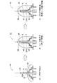
- FIG. 12 is a sub-flowchart showing a sub-process of “sheath thickness control process 1” of FIG. It is a figure which shows an example which applied the different negative bias voltage for every 1 pulse of a microwave pulse. It is an example in which the CPU of the control unit according to the second embodiment changes the voltage value of the negative bias voltage within one microwave pulse. It is a sub-flowchart which shows the sub process of the "sheath thickness control process 2" which CPU of the control part which concerns on 2nd Embodiment performs. It is explanatory drawing explaining the plasma expansion
- the film forming apparatus 1 includes a processing vessel 2, a vacuum pump 3, a gas supply unit 5, a control unit 6, and the like.
- the processing container 2 is made of metal such as stainless steel and has a hermetic structure.
- the vacuum pump 3 is a pump capable of evacuating the inside of the processing container 2 via the pressure adjustment valve 7.
- a conductive material 8 to be deposited is held by a conductive holder 9 made of stainless steel or the like.
- the material of the work material 8 is not particularly limited as long as it has conductivity, but in the first embodiment, it is a low temperature tempered steel.
- the low temperature tempered steel is a material such as JIS G4051 (carbon steel for machine structural use), G4401 (carbon tool steel), G44-4 (alloy tool steel), or maraging steel.
- the workpiece material may be a ceramic or a resin coated with a conductive material.
- the gas supply unit 5 supplies a film forming source gas and an inert gas into the processing container 2. Specifically, an inert gas such as He, Ne, Ar, Kr, or Xe and a source gas such as CH 4 , C 2 H 2 , or TMS (tetramethylsilane) are supplied.
- an inert gas such as He, Ne, Ar, Kr, or Xe
- a source gas such as CH 4 , C 2 H 2 , or TMS (tetramethylsilane) are supplied.
- description will be made assuming that the material to be processed 8 is subjected to the DLC film formation process using the source gases of C 2 H 2 , CH 4 , and TMS.
- the flow rate and pressure of the raw material gas and the inert gas supplied from the gas supply unit 5 may be controlled by the CPU 31 described later, or may be controlled by an operator.
- the source gas may be a gas containing a compound having a CH bond such as alkyne, alkene, alkane, aromatic compound, or a compound containing carbon.
- H 2 may be contained in the raw material gas.
- the plasma for performing the DLC film forming process on the material 8 to be processed held inside the processing container 2 is generated.
- This plasma is generated by the microwave pulse controller 11, the microwave oscillator 12, the microwave power source 13 (see FIG. 2), the negative voltage power source 15, and the negative voltage pulse generator 16.
- the first embodiment will be described on the assumption that surface wave excitation plasma is generated by a method disclosed in Japanese Patent Application Laid-Open No. 2004-47207 (hereinafter, referred to as “MVP method (Microwave Voltage coupled Plasma method)”). In the following description, the MVP method will be described.
- the microwave pulse control unit 11 oscillates a pulse signal in accordance with an instruction from the control unit 6, and supplies the oscillated pulse signal to the microwave oscillator 12.
- the microwave oscillator 12 generates a microwave pulse according to the pulse signal from the microwave pulse controller 11.
- the microwave power supply 13 supplies electric power to the microwave oscillator 12 that oscillates the microwave of 2.45 GHz with the instructed output according to the instruction of the control unit 6. That is, the microwave oscillator 12 supplies a 2.45 GHz microwave to the isolator 17 described later as a pulsed microwave pulse according to the pulse signal from the microwave pulse control unit 11.
- the microwave pulse is transmitted from the microwave oscillator 12 to the isolator 17, the tuner 18, the waveguide 19, the coaxial waveguide 21 protruding from the waveguide 19 through a coaxial waveguide converter (not shown), and It is supplied to the processing surface of the holder 9 and the work material 8 through a microwave supply port 22 made of a dielectric material or the like that transmits microwaves such as quartz.
- the isolator 17 prevents the reflected wave of the microwave from returning to the microwave oscillator 12.
- the tuner 18 matches the impedances before and after the tuner 18 so that the reflected wave of the microwave is minimized.
- the outer peripheral surface of the microwave supply port 22 excluding the upper end surface 22A is covered with a side electrode 23 formed of a metal such as stainless steel.
- the side electrode 23 is fixed to the inner side surface of the processing container 2 by screws or the like, and is electrically connected to the processing container 2.
- a central conductor of the coaxial waveguide 21 is extended at the center of the microwave supply port 22.
- the holder 9 is also on the extension of the central conductor and becomes the central conductor in the microwave supply port 22. Therefore, the central conductor of the microwave supply port 22 and the side electrode 23 function as a coaxial waveguide.
- the microwave propagates to the vicinity of the upper end surface 22A where the holder 9 is provided by the microwave pulse supplied to the microwave supply port 22 to generate plasma. Further, the portion of the workpiece 8 opposite to the holder 9 is arranged so as to protrude toward the inside of the processing container 2 with respect to the microwave supply port 22 and applies a negative bias voltage pulse. Therefore, a negative voltage electrode 25 is electrically connected.
- the central conductor of the microwave supply port 22 is divided in the middle to maintain a vacuum, but may be penetrated if the vacuum is maintained by brazing with a dielectric or the like.
- the workpiece material 8 has, for example, a rod shape, and is held on an extension line of the central conductor of the microwave supply port 22. Instead of the holder 9, a part of the work material 8 may be held so as to be a central conductor in the microwave supply port 22.
- the negative voltage power supply 15 supplies a negative bias voltage to the negative voltage pulse generator 16 in accordance with an instruction from the controller 6.
- the negative voltage pulse generator 16 pulses the negative bias voltage supplied from the negative voltage power supply 15. This pulsing process is a process in which the negative voltage pulse generator 16 controls the magnitude, cycle, and duty ratio of the negative bias voltage pulse in accordance with an instruction from the controller 6.
- a negative bias voltage pulse which is a pulsed negative bias voltage, is applied to the workpiece 8 held inside the processing vessel 2 via the negative voltage electrode 25.
- a negative bias voltage pulse is applied to at least the entire processing surface of the workpiece 8. Applied. Further, a negative bias voltage pulse is also applied to the entire surface of the holder 9 via the workpiece 8.
- the surface wave excitation plasma 45 is generated by controlling the generated microwave pulse and at least a part of the negative bias voltage pulse to be applied at the same time.
- the microwave is not limited to 2.45 GHz but may be any frequency from 0.3 GHz to 50 GHz.
- the negative voltage power supply 15 and the negative voltage pulse generator 16 are examples of the negative voltage application unit of the present invention.
- the microwave control unit 11, the microwave oscillator 12, the microwave power source 13, the isolator 17, the tuner 18, the waveguide 19, the coaxial waveguide 21, and the microwave supply port 22 are examples of the microwave supply unit of the present invention.
- the film forming apparatus 1 includes the negative voltage power supply 15 and the negative voltage pulse generation unit 16, but may include a positive voltage power supply and a positive voltage pulse generation unit, or instead of the negative voltage pulse generation unit 16. In addition, a negative voltage generator that applies a continuous negative bias voltage instead of a pulsed negative bias voltage may be provided.
- the film forming apparatus 1 includes a negative voltage generator that applies a continuous negative bias voltage
- a positive voltage pulse generator If a continuous negative bias voltage is continuously applied to the work material 8, arcing is likely to occur. In order to reduce the occurrence of this arcing, the pulsed positive bias voltage is applied during a period of several percent of the period during which the negative bias voltage is applied during the period during which the negative bias voltage is applied. desirable.
- control unit 6 outputs control signals to the negative voltage power supply 15 and the microwave power supply 13 to control the applied power of the microwave pulse and the applied voltage of the negative voltage pulse.
- the control unit 6 outputs a control signal to the negative voltage pulse generation unit 16 and the microwave pulse control unit 11, thereby generating a pulsed negative bias voltage pulse application timing, a supply voltage, and a microwave oscillator 12. Control the supply timing and power supply of the microwave pulse.
- the control unit 6 outputs a flow rate control signal to the gas supply unit 5 to control the supply of the raw material gas and the inert gas.
- the control unit 6 outputs a control signal to the pressure adjustment valve 7 based on a pressure signal representing the pressure in the processing container 2 input from the vacuum gauge 26 attached to the processing container 2, and Control the pressure.
- the control unit 6 includes a CPU 31, a RAM 32, a ROM 33, a hard disk drive (hereinafter referred to as “HDD”) 34, a timer 35 for measuring time, and a processing time for sub-processing of “sheath thickness control processing 1” shown in FIG. 11.
- An end determination timer 36 and the like for measuring are provided, and the computer is configured.
- the CPU 31 temporarily stores various information in a volatile storage device such as the RAM 32, and executes a program such as a film forming process shown in FIG.
- the ROM 33 and the HDD 34 are non-volatile storage devices, and include a program such as a film forming process shown in FIG. 11, application timings of microwave pulses and negative bias voltage pulses shown in FIG. 9, an applied voltage table 55 shown in FIG. I remember it.
- control unit 6 includes a pressure adjusting valve 7, a vacuum gauge 26, a negative voltage power supply 15, a negative voltage pulse generation unit 16, a microwave pulse control unit 11, a gas supply unit 5, and a microwave power supply 13. It is connected. 11 may be read from a storage medium such as a CD-ROM or DVD-ROM by a driver (not shown), or may be downloaded from a network such as the Internet (not shown).
- an essentially unipolar charged particle layer a so-called sheath layer
- the sheath layer is a layer having a low electron density, that is, positive polarity, and substantially has a relative dielectric constant in the microwave frequency band. It is a layer of ⁇ 1.
- the sheath thickness of the sheath layer can be increased by making the absolute value of the negative bias voltage to be applied larger than the absolute value of, for example, ⁇ 100V. That is, the sheath layer expands.
- This sheath layer acts as a dielectric that propagates surface waves to the interface between the plasma and the object in contact with the plasma.
- the microwave is supplied from the microwave supply port 22 disposed in the vicinity of one end of the holder 9 that holds the workpiece 8, and a negative bias voltage is applied to the workpiece 8 and the holder 9. Then, the microwave propagates as a surface wave along the interface between the sheath layer and the plasma. As a result, high-density excitation plasma based on surface waves is generated along the surfaces of the workpiece 8 and the holder 9. This high-density excitation plasma is the surface wave excitation plasma 45 described above.
- the electron density of the high-density plasma due to surface wave excitation in the vicinity of the surface of the workpiece 8 reaches 10 11 to 10 12 cm ⁇ 3 .
- the film formation speed is 3 to 30 times higher by one to two orders of magnitude than when the DLC film formation process is performed by plasma CVD with a normal negative bias voltage energy. (Nano m / sec) is obtained.
- the plasma CVD film formation time by the MVP method is 1/10 to 1/100 of the normal plasma CVD film formation time.
- the work material 8 is formed in a columnar shape having a diameter of 10 mm.
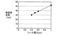
- the wavelength of the surface wave when the sheath thickness is about 0.4 mm is about 30 mm.
- the wavelength of the surface wave when the sheath thickness is about 0.6 mm is about 39 mm.
- the wavelength of the surface wave when the sheath thickness is about 1.0 mm is about 52 mm. Therefore, the wavelength of the surface wave becomes longer as the sheath thickness of the sheath layer increases. That is, the wavelength of the surface wave can be increased by increasing the sheath thickness of the sheath layer, and the wavelength of the surface wave can be shortened by decreasing the sheath thickness of the sheath layer.
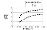
- the black circles represent data when the workpiece 8 is a cylinder with a diameter of 1 mm.
- Black square marks represent data when the workpiece 8 is a cylinder having a diameter of 10 mm.
- the wavelength of the surface wave when the workpiece 8 has a diameter of 1 mm is about 39 mm
- the workpiece 8 is The wavelength of the surface wave when the diameter is 10 mm is about 19 mm.
- the wavelength of the surface wave when the workpiece 8 has a diameter of 1 mm is about 73 mm
- the surface wave when the workpiece 8 has a diameter of 10 mm is used.
- the wavelength is about 52 mm. Therefore, the wavelength of the surface wave becomes longer as the plasma electron density increases. That is, by increasing the microwave output and increasing the plasma electron density, the surface wave wavelength can be increased, and by reducing the microwave output and reducing the plasma electron density, the surface Wave wavelengths can be shortened.
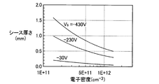
- the negative bias voltage was 0V, ⁇ 200V, ⁇ 400V, and the plasma potential was + 30V. Therefore, the plasma electron density and the sheath thickness of the sheath layer were analyzed for sheath potentials of about ⁇ 30 V, about ⁇ 230 V, and about ⁇ 430 V, which are potentials of the workpiece 8 with respect to the plasma potential.
- the sheath thickness of the sheath layer when the negative bias voltage is ⁇ 30 V is about 0.1 mm
- the sheath thickness of the sheath layer when the bias voltage is ⁇ 230 V is about 0.5 mm
- the sheath thickness of the sheath layer when the negative bias voltage is ⁇ 430 V is about 0.9 mm.
- the sheath thickness of the sheath layer when the negative bias voltage is ⁇ 30V is about 0.06 mm
- the sheath thickness when the negative bias voltage is ⁇ 230V is about 0.4 mm
- the sheath thickness of the sheath layer when the negative bias voltage is ⁇ 430 V is about 0.6 mm.
- the sheath thickness of the sheath layer increases as the negative bias voltage increases.
- the sheath thickness of the sheath layer can be increased by increasing the negative bias voltage.
- the sheath thickness of the sheath layer can be reduced.
- FIG. 6 (A) the discontinuous shape in the vertical direction in FIG. 6 (A), which is the microwave supply direction, at the connection portion between the tip of the workpiece 8 and the negative voltage electrode 25.
- the discontinuous portion 41 is formed, the sheath layer 42 formed on the surface around the discontinuous portion 41 has a discontinuous shape. Therefore, the microwave propagating as a surface wave in the sheath layer 42 is reflected by a discontinuous portion of the sheath layer 42 formed around the discontinuous portion 41 and supplied from the upper end surface 22A of the microwave supply port 22. Interfering with surface waves generated by microwaves to generate standing waves.
- the surface wave reflected by the discontinuous portion 41 generates the standing wave 43 at a wavelength determined by the sheath thickness, the electron density of the plasma, and the diameter of the workpiece 8.
- the surface wave-excited plasma 45 is density-distributed in 1/2 period of the standing wave 43. Therefore, in the plasma density distribution of the surface wave excitation plasma 45, several nodes having low plasma density are generated in the microwave supply direction of the material 8 to be processed, and a local maximum where the plasma density is maximum is generated between the nodes. To do.
- the wavelength of the surface wave propagating in the sheath layer 42 becomes longer as shown in FIG. .
- the wavelength of the standing wave 44 generated is also increased, and the surface wave excitation plasma 45 is constant. 1/2 of standing wave 46 Density wave distribution with period. Therefore, in the plasma density distribution of the surface wave excitation plasma 45, a smaller number of nodes having a lower plasma density than the plasma density nodes shown in FIG. 7A are generated, and between the nodes and above the microwave supply port 22. A local maximum where the plasma density is maximum occurs in the vicinity of the end face 22A.
- the wavelength of the surface wave is about 30 mm.
- the negative bias voltage at this time is about ⁇ 200 V (the sheath potential is ⁇ 230 V).
- the negative bias voltage is about ⁇ 358 V (sheath potential is ⁇ 388 V) from FIG.
- the sheath thickness is about 0.57 mm.
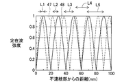
- the standing wave generated by the surface wave reflected by the discontinuous portion 41 has the standing wave 47 when the surface wave wavelength is about 30 mm and the wavelength of the surface wave. It changes between the standing wave 48 at about 37.5 mm. Accordingly, since the plasma density distribution of the surface wave excited plasma 45 changes between the standing wave 47 and the standing wave 48, the position where the plasma density becomes maximum and the position where the plasma density becomes minimum during film formation. And fluctuate. Therefore, the film characteristics such as the film thickness and film hardness of the DLC film formed on the processing surface of the work material 8 can be made uniform.
- the vertical axis indicates the relative standing wave intensity
- the horizontal axis indicates the distance from the discontinuous portion 41.
- the plasma density distribution of the surface wave excited plasma 45 is 1 / of each of the standing waves 47 and 48. Density wave distribution in two cycles. Therefore, the distance from the discontinuous portion 41 of each local maximum where the plasma density generated by the standing wave 47 is maximum is about 7.5 mm, about 22.5 mm, about 37.5 mm, about 52.5 mm, about It occurs at a position of 67.5 mm.
- FIG. 6 (B) it has a continuous shape with the work material 8 between the tip of the work material 8 and the negative voltage electrode 25, and has a predetermined length (for example, a length of about
- the conductive connecting member 49 made of stainless steel or the like may be provided.
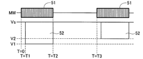
- the period of the microwave pulse 51 is T3 (seconds).
- the supply time for each pulse of the microwave pulse 51 is T2 (seconds).
- T2 is set to about 1 ⁇ 2 of T3.
- the cycle of the negative bias voltage pulse 52 is the same cycle as the cycle of the microwave pulse 51 and is T3 (seconds).
- the application time of the negative bias voltage pulse 52 is (T2-T1) (seconds), and is set to 90% or more of the supply time T2 (seconds) of the microwave pulse 51.
- the application timing of the negative bias voltage pulse 52 is set so as to be delayed by T1 (seconds) from the supply start timing of the microwave pulse 51. That is, the negative bias voltage pulse 52 is applied after the microwave pulse 51 rises and the power is stabilized.
- the delay time T1 8 (microseconds).
- Information indicating the times T1, T2, and T3 (seconds) is stored in the ROM 33 or the HDD 34.
- the applied voltage table 55 includes “order”, “microwave output (kW)”, and “negative bias voltage (V)”. In this “order”, the orders “1” to “M” (the number of times) for supplying the microwave pulses are stored.
- a microwave output of 2.45 GHz is stored in association with the “order” in which the microwave pulses 51 are supplied. In the first embodiment, it is a constant value of approximately 1 (kW).
- negative bias voltage (V) the negative applied voltage value of the negative bias voltage pulse 52 applied to the negative voltage electrode 25 is stored in association with the “order” in which the microwave pulses 51 are supplied. Has been. That is, the negative applied voltage value of the negative bias voltage pulse 52 set so as to change the sheath thickness of the sheath layer 42 within a predetermined range is associated with the “order” in which the microwave pulse 51 is supplied. It is remembered.
- the negative applied voltage value is changed from about ⁇ 200 V to about ⁇ 200 V so that the sheath thickness of the sheath layer 42 is changed between about 0.4 mm and about 0.57 mm.
- a negative applied voltage value changed at a constant cycle or randomly between ⁇ 358 V is stored in association with the “order” in which the microwave pulse 51 is supplied.
- step (hereinafter abbreviated as “S”) 11 the CPU 31 stores information indicating the period T ⁇ b> 3 (seconds) of the microwave pulse 51 shown in FIG. 9 from the ROM 33 or HDD 34.
- Information indicating the supply time T2 (seconds) is read and stored in the RAM 32.
- the period T3 of the microwave pulse 51 is 2 (milliseconds)
- the supply time T2 for each pulse is 1 (milliseconds).
- the applied voltage table 55 and ion cleaning parameters described later are also read from the ROM 33 or the HDD 34 and stored in the RAM 32.
- the CPU 31 receives information indicating the period T3 (seconds) of the negative bias voltage pulse 52 shown in FIG. 9 from the ROM 33 or the HDD 34, information indicating the application time (T2-T1) (seconds) for each pulse, and microwave pulses.
- Information indicating the delay time T1 (seconds) from the supply start timing of 51 is read out and stored in the RAM 32.
- the period T3 of the negative bias voltage pulse 52 is 2 (milliseconds)
- the application time (T2-T1) per pulse is 992 (microseconds)
- the delay time T1 is 8 (microseconds). is there.
- the delay time T1 may be set to about 5 (microseconds) to 20 (microseconds).
- Each time T1, T2, and T3 (seconds) may be input to the control unit 6 of the film forming apparatus 1 by an operator via an operation unit (not shown).
- the CPU 31 reads out predetermined parameters from the ROM 33 or the HDD 34, stores them in the RAM 32, and activates the vacuum pump 3.
- the predetermined parameters are parameters such as an ion cleaning parameter and a gas flow rate value. These parameters may be set manually by an operator, or may be set automatically based on parameters stored in the ROM 33 or the HDD 34 in advance.
- the ion cleaning parameter is a parameter for an ion cleaning process described later.
- the CPU 31 determines whether or not the inside of the processing container 2 has a predetermined degree of vacuum (for example, less than 1.0 Pa). A determination process for determining is executed. This predetermined degree of vacuum is stored in advance in the ROM 33 or the HDD 34. And when it determines with the inside of the processing container 2 not having reached the predetermined degree of vacuum (S13: NO), CPU31 performs the process of S13 again.
- a predetermined degree of vacuum for example, less than 1.0 Pa.
- the CPU 31 proceeds to the process of S14.
- the CPU 31 reads out the gas flow rate value of the inert gas Ar that is an ion cleaning parameter (for example, the gas flow rate is 200 sccm) from the RAM 32, and processes the gas flow rate value read out to the gas supply unit 5.
- a supply signal instructing to supply the inert gas Ar into the container 2 is output. That is, the supply of the inert gas Ar is started.
- the CPU 31 sets the raw material gas and the inert gas in the processing container 2 to be exhausted at a constant flow rate via the pressure adjustment valve 7, and adjusts the inside of the processing container 2 to a predetermined pressure. To do. Subsequently, in S ⁇ b> 16, the CPU 31 executes determination processing for determining whether or not the inside of the processing container 2 has reached a predetermined pressure based on the pressure signal input from the vacuum gauge 26. And when it determines with the inside of the processing container 2 not having reached the predetermined pressure (S16: NO), CPU31 performs the process after S15 again.
- the CPU 31 proceeds to the process of S17.
- the CPU 31 starts ion cleaning based on the ion cleaning parameter.
- the ion cleaning parameters include microwave output power (for example, 800 W power) and negative bias voltage pulse applied voltage (for example, ⁇ 200 V).
- the CPU 31 transmits the applied voltage of the negative bias voltage pulse to the negative voltage power supply 15.
- the CPU 31 transmits microwave output power to the microwave power source 13.
- the CPU 31 performs the period T3 (seconds) of the negative bias voltage pulse 52 acquired in S11, the application time (T2-T1) (seconds) for each pulse, and the delay time T1 from the supply start timing of the microwave pulse 51.
- an ON signal and an OFF signal of the negative bias voltage pulse 52 are transmitted to the negative voltage pulse generator 16.
- the CPU 31 converts the on signal and the off signal of the microwave pulse 51 based on the period T3 (second) of the microwave pulse 51 acquired in S11 and the supply time T2 (second) for each pulse. Send to.
- the negative voltage power supply 15 supplies a negative applied voltage to the negative voltage pulse generator 16 according to the received applied voltage.
- the negative voltage pulse generation unit 16 uses the supplied negative applied voltage and the ON signal and the OFF signal of the negative bias voltage pulse 52 received every cycle T3 (seconds) to start T1 ( (Second), and a negative bias voltage pulse 52 is applied to the workpiece 8 via the negative voltage electrode 25 for (T2-T1) seconds.
- the microwave power source 13 supplies power to the microwave oscillator 12 according to the received microwave output power.
- the microwave pulse control unit 11 transmits a pulse signal for the supply time T2 (seconds) to the microwave oscillator 12 every period T3 (seconds) according to the ON signal and the OFF signal of the received microwave pulse 51.
- the microwave oscillator 12 generates a microwave pulse 51 having a supply time T2 (seconds) according to the received pulse signal at a period T3 (seconds) with a microwave power of 2.45 GHz corresponding to the supplied power.
- the sheath layer 42 along the surface of the material 8 to be processed by these negative bias voltage pulses 52 is in a direction orthogonal to the propagation direction of the microwave, that is, FIG.
- the plasma of the inert gas Ar is generated by the microwave pulse 51 that is expanded in the horizontal direction and propagates in the sheath layer 42.
- the surface of the material 8 to be processed is ion-cleaned by the generated plasma of the inert gas Ar, and a DLC film described later is easily formed.
- the CPU 31 proceeds to the process of S18.
- the CPU 31 determines whether or not to finish the ion cleaning. This determination is made based on whether or not the arcing occurrence frequency is less than a predetermined frequency.
- the predetermined frequency is stored in advance in the ROM 33 or the HDD 34. When it is determined that the arcing occurrence frequency is equal to or higher than the predetermined frequency (S18: NO), the CPU 31 executes the process of S18 again.
- the CPU 31 proceeds to the process of S19.
- This end determination may be made by determining whether or not the ion cleaning time is set as an ion cleaning parameter and the time measured by the timer 35 from the start of ion cleaning has passed the ion cleaning time.
- the CPU 31 transmits a stop signal instructing the microwave pulse control unit 11 to stop the pulse signal transmitted to the microwave oscillator 12. Thereby, since the microwave oscillator 12 does not receive the pulse signal, the output of the microwave pulse 51 is stopped. Further, the CPU 31 transmits a stop signal that instructs the negative voltage pulse generator 16 to stop the application of the negative bias voltage pulse 52. As a result, the negative voltage pulse generator 16 stops applying the negative bias voltage pulse 52 to the workpiece 8.
- the CPU 31 reads out the respective gas flow values for supplying the source gas and the inert gas from the ROM 33 or the HDD 34, transmits them to the gas supply unit 5 as flow control instructions, and then proceeds to the processing of S21.
- the gas supply unit 5 supplies the source gas and the inert gas into the processing container 2 in accordance with the flow control instruction.
- each gas flow value which supplies raw material gas and an inert gas is memorize
- the inert gas Ar is 40 sccm.
- CH 4 is a 200sccm.
- C 2 H 2 is 0 sccm.
- TMS is 20 sccm.
- the CPU 31 sets the raw material gas and the inert gas in the processing container 2 to be exhausted at a constant flow rate via the pressure adjustment valve 7, and adjusts the inside of the processing container 2 to a predetermined pressure.
- the CPU 31 determines whether or not the inside of the processing container 2 has reached a predetermined pressure, that is, the flow rates of the source gas and the inert gas. A determination process for determining whether or not the object is stable is executed. And when it determines with the inside of the processing container 2 not having reached the predetermined pressure (S22: NO), CPU31 performs the process after S21 again.
- the CPU 31 reads the count value N of the number counter from the RAM 32 in S23, and this count value “1” is substituted into N and stored in the RAM 32 again. That is, the CPU 31 initializes the count value of the number counter. At the same time, the CPU 31 starts measuring the processing time after resetting the measurement time of the end determination timer 36 to “0”.
- the CPU 31 executes the sub-process shown in FIG. 12, which is the “sheath thickness control process 1” for changing the sheath thickness for each pulse of a microwave pulse 51 described later, and then the process in S25.
- the CPU 31 executes a determination process for determining whether or not the film forming process for forming the DLC film on the surface of the work material 8 has been completed.
- the CPU 31 reads information indicating the processing time of the sub-process of “sheath thickness control process 1” executed in S24 from the ROM 33 or the HDD 34, and whether or not the end determination timer 36 has reached the processing time.
- a determination process is performed to determine whether or not.
- the processing time of the sub-process of “Sheath thickness control process 1” executed in S24 may be set manually by an operator, or automatically set based on parameters stored in the ROM 33 or HDD 34 in advance. Good.
- the CPU 31 transmits a supply stop signal that instructs the gas supply unit 5 to stop the supply of the source gas and the inert gas.
- the CPU 31 transmits an exhaust signal that instructs the pressure adjustment valve 7 to fully open the exhaust.
- the gas supply part 5 stops supply of the raw material gas and the inert gas to the inside of the processing container 2 according to a supply stop signal.
- the pressure adjusting valve 7 is fully opened, and the raw material gas and the inert gas remaining in the processing container 2 are immediately exhausted by the vacuum pump 3. Thereafter, the CPU 31 ends the process.
- the CPU 31 transmits the output power of the microwave to the microwave power source 13.
- the CPU 31 transmits a microwave pulse on signal to the microwave pulse control unit 11.
- the microwave power supply 13 supplies power to the microwave oscillator 12 according to the received microwave output power, that is, supplies an applied voltage and an anode current applied to the magnetron in the microwave oscillator 12.
- the microwave pulse control unit 11 starts transmission of a pulse signal for the supply time T2 (seconds) to the microwave oscillator 12 in accordance with the received information indicating the supply time T2 (seconds) together with the processing of S116 described later. .
- the microwave oscillator 12 supplies a 2.45 GHz microwave pulse 51 of supply time T2 (seconds) with the supplied power to the isolator 17, the tuner 18, the waveguide 19, the coaxial waveguide 21, and the microwave supply port.
- the supply to the holder 9 and the workpiece material 8 is started via 22.
- the CPU 31 executes a determination process for determining whether the measurement time of the timer 35 has reached the delay time T1 (seconds), that is, whether the application timing of the negative bias voltage pulse 52 has been reached. To do.
- the CPU 31 executes the process of S113 again.
- the CPU 31 proceeds to the process of S114.
- S ⁇ b> 114 the CPU 31 sets the count value N of the number counter as “order” in the applied voltage table 55 shown in FIG. 10, and the negative bias voltage of “negative bias voltage (V)” associated with this “order”.
- the pulse application voltage is read from the application voltage table 55.
- the CPU 31 transmits the applied voltage of this negative bias voltage pulse to the negative voltage power supply 15.
- the CPU 31 transmits a negative bias voltage pulse on signal to the negative voltage pulse generator 16.
- the negative voltage power supply 15 supplies a negative voltage to the negative voltage pulse generator 16 according to the received applied voltage.
- the negative voltage pulse generation unit 16 applies a negative bias voltage pulse 52 that is applied to the negative applied voltage and has an application time (T2 ⁇ T1) (seconds) in combination with the process of S116 described later. Then, application to the work material 8 is started.
- the CPU 31 executes a determination process for determining whether the measurement time of the timer 35 has reached the supply time T2 (seconds) of the microwave pulse 51.
- the CPU 31 executes the process of S115 again.
- the CPU 31 proceeds to the process of S116.
- the CPU 31 transmits a microwave pulse-off signal that instructs the microwave pulse control unit 11 to stop the pulse signal transmitted to the microwave oscillator 12. Thereby, since the microwave oscillator 12 does not receive the pulse signal, the output of the microwave pulse 51 is stopped.
- the CPU 31 transmits a negative bias voltage pulse off signal that instructs the negative voltage pulse generator 16 to stop applying the negative bias voltage pulse 52. As a result, the negative voltage pulse generator 16 stops applying the negative bias voltage pulse 52 to the workpiece 8.
- the CPU 31 executes a determination process for determining whether or not the measurement time of the timer 35 has reached the period T3 (seconds) of the microwave pulse 51.
- the CPU 31 executes the process of S117 again.
- the CPU 31 proceeds to the process of S118.
- the CPU 31 executes a determination process for determining whether or not the count value N of the number counter has reached “M” which is the final number of “order” in the applied voltage table 55.
- M the number of the number counter
- the CPU 31 proceeds to the process of S119.
- S119 after adding “1” to the count value N of the number counter, the CPU 31 ends the sub-process, returns to the main flowchart, and proceeds to the process of S25.
- control processing 1 when the electron density of plasma inside the processing container 2 is 10 12 cm ⁇ 3 , the sheath thickness of the sheath layer 42 is changed from about 0.4 mm to about 0.57 mm, and the film is formed.
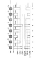
- control processing 1 As shown in FIG. 13, every time one microwave pulse 51 with a microwave output power of about 1 kW is supplied, a negative bias voltage pulse with a negative applied voltage of ⁇ 358 V (the sheath potential is ⁇ 388 V).
- negative bias voltage pulse 52A negative bias voltage pulse 52B with negative applied voltage of ⁇ 279V (sheath potential is ⁇ 309V)
- negative bias voltage pulse 52C with negative applied voltage of ⁇ 200V (sheath potential of ⁇ 230V)
- negative A negative bias voltage pulse 52D having an applied voltage of ⁇ 279 V is repeatedly applied to the workpiece 8 in order.
- the sheath thickness of the sheath layer 42 generated on the surface of the work material 8 is about 0.57 mm, about 0.57 mm for each one pulse of each microwave pulse 51 whose microwave output power is about 1 kW. It can be repeatedly changed in the order of 0.49 mm, about 0.4 mm, and about 0.49 mm. Thereby, the wavelength of the surface wave propagating in the sheath layer 42 is repeatedly changed in order of about 37.5 mm, about 33.8 mm, about 30 mm, and about 33.8 mm.
- the standing wave changes for each wavelength of the surface wave
- the plasma density distribution of the surface wave excited plasma 45 changes for each standing wave. That is, in the longitudinal direction of the work material 8, that is, in the microwave supply direction, the position where the plasma density increases and the position where the plasma density decreases sequentially change and the plasma density is averaged. The uniformity of density distribution is improved. For this reason, the film characteristics such as the film thickness and film hardness of the DLC film formed on the processing surface of the workpiece 8 can be made uniform.
- the CPU 31 applies the negative bias voltage pulse 52 to the work material 8 via the negative voltage electrode 25 while the microwave pulse 51 is being supplied. Apply to generate sheath layer 42. Further, by changing the applied voltage of the negative bias voltage pulse 52 for each pulse of the microwave pulse 51, the sheath thickness of the sheath layer 42 is changed, and the inside of the sheath layer 42 is changed to a surface wave with a high energy density. The distribution of standing waves generated by propagating microwaves can be changed.
- the standing wave distribution of the plasma density of the high-density plasma of the source gas plasma-excited by the surface wave can be changed, and the propagation of the surface wave propagating in the longitudinal direction of the workpiece 8, that is, in the sheath layer 42. Since the plasma density with respect to the direction is averaged and made uniform, film characteristics such as the film thickness and film hardness of the DLC film formed on the surface of the work material 8 can be made uniform.
- the DLC film formed on the surface of the workpiece 8 is changed by changing the sheath thickness of the sheath layer 42 and changing the wavelength of the surface wave propagating in the sheath layer 42 by a quarter wavelength or more. Film characteristics such as film thickness and film hardness can be made more uniform.
- each pulse of the microwave pulse 51 plural kinds of pulsed negative bias voltage pulses 52 having different negative applied voltages are sequentially applied to repeat expansion and reduction of the sheath thickness.
- the averaged plasma density distribution is made uniform by constantly changing the distribution of the standing wave generated by the microwave propagating as a high energy density surface wave in the sheath layer 42.
- the film characteristics such as the film thickness and film hardness of the DLC film formed on the surface of the material to be processed can be made more uniform.
- the sheath thickness of the sheath layer 42 is changed in order to change the sheath thickness by changing the negative applied voltage of the negative bias voltage pulse 52 applied to the workpiece 8 during the supply of the microwave pulse 51. It can be changed at high speed. Thereby, the distribution change of the standing wave generated by the microwave propagating in the sheath layer 42 as a surface wave with a high energy density can be performed at high speed, and the followability to high-speed film formation by the MVP method can be improved. it can. That is, in the MVP method, a processing time of about several tens of seconds is required to form a DLC film of about 1 to 2 ⁇ m. During this time, the thickness of the sheath layer 42 can be changed at high speed.
- FIGS. 1 to 13 the same reference numerals as those of the film forming apparatus 1 according to the first embodiment in FIGS. 1 to 13 denote the same or corresponding parts as those of the film forming apparatus 1 according to the first embodiment. It is shown.
- the contour of the surface wave excited plasma 66 is actually wavy due to the influence of standing waves. Further, the actual size of the surface wave excited plasma 66 is not necessarily the size of the surface wave excited plasma 66 shown in FIG.
- the schematic configuration of the film forming apparatus 61 according to the second embodiment is substantially the same as the film forming apparatus 1 according to the first embodiment.
- the application timing of the microwave pulse 51 and the negative bias voltage pulse 52 shown in FIG. 9 the application timing of the microwave pulse 51 and the negative bias voltage pulse 62 shown in FIG. It is remembered.
- the initial applied voltage VA which is “0V” of the negative bias voltage pulse 62 shown in FIG. 14, the negative sheath layer initial enlarged applied voltage VB, and the negative sheath.
- the layer normal enlargement applied voltage VC is stored in the ROM 33 or the HDD 34. That is, the applied voltage waveform for each pulse of the negative bias voltage pulse 62 is substantially the same waveform.
- the negative sheath layer initial expansion applied voltage VB is a voltage for extending the negative sheath layer from the peripheral edge of the microwave supply port 22 over the entire work material 8.
- the negative sheath layer normal enlargement applied voltage VC is a voltage for enlarging and maintaining the negative sheath layer extended over the entire work material 8. Accordingly, the negative sheath layer initial enlarged applied voltage VB extends the sheath layer generated at the peripheral edge of the microwave supply port 22 over the entire work material 8, so that the negative sheath layer initial enlarged applied voltage VC is higher than the negative sheath layer normal enlarged applied voltage VC. large.
- the negative sheath layer initial enlarged applied voltage VB is set to an applied voltage larger than the negative sheath layer normal enlarged applied voltage VC.
- the negative sheath layer initial enlarged applied voltage VB ⁇ 400 V (the sheath potential is ⁇ 430 V)
- the negative sheath layer normal enlarged applied voltage VC ⁇ 200 V (the sheath potential is ⁇ 230 V).
- the CPU 31 replaces the sub-process of “sheath thickness control process 1” shown in FIG. 12 with a sub-process of “sheath thickness control process 2” shown in FIG. Execute the process.
- the microwave pulse 51 has the same pulse waveform as the microwave pulse 51 of the film forming apparatus 1 according to the first embodiment.
- the cycle of the negative bias voltage pulse 62 is the same as the cycle of the microwave pulse 51.
- the application timing of the negative bias voltage pulse 62 is the same as the application timing of the negative bias voltage pulse 52 of the film forming apparatus 1 according to the first embodiment. Subsequently, the negative sheath voltage initial enlarged applied voltage VB is applied to the negative bias voltage pulse 62 during the application time (T11-T1). For example, the application time (T11-T1) of the negative sheath layer initial enlarged application voltage VB is 10 (microseconds).
- the negative bias voltage pulse 62 is applied with the negative sheath layer normal expansion applied voltage VC during the application time (T2-T11). Further, the application time (T2-T11) of the negative sheath layer normal expansion application voltage VC is 90% or more of the supply time T2 (seconds) of the microwave pulse 51. For example, the application time (T2-T11) of the negative sheath layer normal expansion application voltage VC is 982 (microseconds). In other words, within one pulse of the microwave pulse 51, the negative bias voltage pulse 62 includes a negative applied voltage VA that is “0 V”, a negative sheath layer initial enlarged applied voltage VB, and a negative sheath layer normal enlarged applied voltage VC. The voltage value changes in the order of.
- the delay time T1 (second) of the negative bias voltage pulse 62, the application time (T11-T1) (second) of the negative sheath layer initial expanded application voltage VB, the negative Application start time T11 (second) of sheath layer normal expansion application voltage VC, application time of negative sheath layer normal expansion application voltage VC (T2-T11) (second), application end time of negative sheath layer normal expansion application voltage VC T2 (seconds) is stored in the ROM 33 or the HDD 34.
- the voltage VC is read and stored in the RAM 32.
- the negative voltage power supply 15 supplies 0 (V) to the negative voltage pulse generator 16 according to the received initial applied voltage VA which is “0 V”.
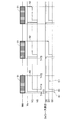
- the negative voltage pulse generation unit 16 starts applying the voltage 0 (V) to the workpiece material 8 through the negative voltage electrode 25. Accordingly, as shown in the left end of FIG. 16 by the microwave pulse 51 that has been started, when the plasma of the source gas and the inert gas is ignited at the peripheral edge of the microwave supply port 22 in the processing container 2, 14, a sheath layer having a sheath thickness D1 (mm) is formed on the surfaces of the workpiece 8 and the holder 9. For example, since the sheath thickness D1 is 0.07 mm and is not enlarged, the microwave does not propagate in the sheath layer as a surface wave. In FIG. 16, the plasma 63 shows only the position where the plasma is generated, and does not show a standing wave. Actually, the density distribution of the plasma is generated according to the standing wave.
- the CPU 31 executes the process of S113. If it is determined that the measurement time of the timer 35 has reached the delay time T1 (seconds) (S213: YES), the CPU 31 proceeds to the process of S214.
- the CPU 31 reads the negative sheath layer initial enlarged applied voltage VB from the RAM 32 and transmits this negative sheath layer initial enlarged applied voltage VB to the negative voltage power supply 15.
- the CPU 31 transmits a negative bias voltage pulse on signal to the negative voltage pulse generator 16.
- negative sheath layer initial enlarged applied voltage VB ⁇ 400 V (sheath potential is ⁇ 430 V)
- application time (T11 ⁇ T1) 10 (microseconds). Further, the supply of the microwave pulse 51 from the microwave oscillator 12 is continued.
- the negative voltage power supply 15 supplies the negative sheath layer initial enlarged applied voltage VB to the negative voltage pulse generator 16 in accordance with the received negative sheath layer initial enlarged applied voltage VB.
- the negative voltage pulse generation unit 16 uses the supplied negative sheath layer initial enlarged applied voltage VB, and a negative bias voltage pulse 62 that has an application time (T11-T1) (seconds) in combination with the processing of S216 described later. Application to the workpiece 8 is started via the negative voltage electrode 25.
- a sheath layer having a sheath thickness D2 (mm) is formed on the surfaces of the workpiece 8 and the holder 9.
- the sheath thickness D2 0.57 mm.
- the microwave propagates as a surface wave in the sheath layer 65 formed and enlarged on the surfaces of the workpiece 8 and the holder 9, and the workpiece 8 and the holder A surface wave excitation plasma 66 which is a high density plasma is generated along the surface 9. That is, since the sheath layer 65 is sufficiently enlarged and the microwave easily propagates as a surface wave, a stable high-density plasma is generated promptly toward the tip of the workpiece 8. Thereby, the formation of the DLC film on the surface of the work material 8 also starts.
- the CPU 31 determines whether or not the measurement time of the timer 35 has reached the application start time T11 (second) of the negative sheath layer normal expansion application voltage VC, that is, the negative sheath layer normal expansion application voltage VC. A determination process for determining whether or not the application timing has come is executed. If it is determined that the measurement time of the timer 35 has not reached the application start time T11 (seconds) of the negative sheath layer normal expansion application voltage VC (S215: NO), the CPU 31 executes the process of S215 again. To do.
- the CPU 31 proceeds to the process of S216.
- S ⁇ b> 216 the CPU 31 reads the negative sheath layer normal enlargement applied voltage VC from the RAM 32 and transmits it to the negative voltage power supply 15.
- the CPU 31 transmits a negative bias voltage pulse on signal to the negative voltage pulse generator 16.
- the negative sheath layer normal enlarged applied voltage VC ⁇ 200 V (sheath potential is ⁇ 230 V)
- the application time (T2 ⁇ T11) is 982 (microseconds). Further, the supply of the microwave pulse 51 from the microwave oscillator 12 is continued.
- the negative voltage power supply 15 supplies the negative sheath layer normal expansion application voltage VC to the negative voltage pulse generator 16 in accordance with the received negative sheath layer normal expansion application voltage VC.
- the negative voltage pulse generator 16 applies a negative bias voltage pulse 62, which is applied to the negative sheath layer normal expanded applied voltage VC, together with the processing of S218, which will be described later, and has an application time (T2-T11) (seconds). Application is made to the workpiece 8 through the voltage electrode 25.
- a sheath layer having a sheath thickness D3 (mm) is formed on the surface of the workpiece 8 and the holder 9.
- the sheath thickness D3 0.4 mm.
- the microwave propagates as a surface wave in the sheath layer 67 formed on the surfaces of the workpiece 8 and the holder 9, and the workpiece 8 and the holder 9.
- a surface wave excitation plasma 66 that is a high-density plasma is generated along the surface.
- a DLC film is formed on the surface of the work material 8.
- the CPU 31 executes the process of S115.
- the CPU 31 proceeds to the process of S218.
- the CPU 31 executes the process of S116.
- the CPU 31 executes the process of S117.
- the CPU 31 proceeds to the process of S220.
- the CPU 31 reads the total number of application times M from the ROM 33 or the HDD 34, and executes a determination process for determining whether or not the count value N of the number counter has reached the total number of application times M. If it is determined that the count value N of the number counter has not reached the total number of application times M (S220: NO), the CPU 31 proceeds to the process of S221. In S221, the CPU 31 executes the process of S119. On the other hand, when it is determined that the count value N of the number counter has reached the total application number M (S220: YES), the CPU 31 proceeds to the process of S222. In S222, the CPU 31 executes the process of S120.
- the CPU 31 applies the negative bias voltage pulse 62 to “0V” within the supply time T2 (second) for each pulse of the microwave pulse 51.
- the voltage is changed with the application time (T2-T11) (seconds).
- the sheath layer 65 having a large sheath thickness is generated by applying a negative sheath layer initial expansion applied voltage VB to the workpiece 8,
- the surface wave excitation plasma can be extended at high speed.
- a sheath layer 67 having a predetermined thickness is generated on the surface of the work material 8 by applying a negative sheath layer normal expansion applied voltage VC to the work material 8, and the surface wave excitation plasma 66 is stably generated.
- the surface wave excitation plasma can be extended at a high speed along the surface of the material 8 to be processed, and the followability to the high-speed film formation by the MVP method can be improved.
- FIGS. 1 to 13 the same reference numerals as those of the film forming apparatus 1 according to the first embodiment in FIGS. 1 to 13 denote the same or corresponding parts as those of the film forming apparatus 1 according to the first embodiment. It is shown.
- the schematic configuration of the film forming apparatus 71 according to the third embodiment is substantially the same as the film forming apparatus 1 according to the first embodiment.
- the “negative bias voltage (V)” in the applied voltage table 55 shown in FIG. 10 is associated with the “order” in which the microwave pulse 51 is supplied, and the sheath layer 42.
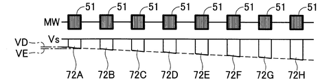
- the negative applied voltage values of the negative bias voltage pulses 72A, 72B, 72C,... Set so as to gradually increase the sheath thickness within a predetermined range are stored. Further, each negative applied voltage value gradually increases from the initial voltage VD to the final voltage VE so that the negative applied voltage value of each bias voltage pulse 72A, 72B, 72C,... Continuously changes. Is set to
- the initial voltage VD and the final voltage of the negative applied voltage are gradually increased so that the sheath thickness of the sheath layer 42 gradually increases from about 0.4 mm to about 0.57 mm.
- the CPU 31 executes the sub-process of “sheath thickness control process 1” in S24 of the “film formation process”, it is applied to the workpiece 8 through the negative voltage electrode 25 in S114.
- the absolute value of the negative applied voltage gradually increases with each application and gradually increases during the application.
- the sheath thickness of the sheath layer 42 formed on the surface of the workpiece material 8 gradually increases every time a negative applied voltage is applied, and gradually increases during the application. A DLC film is formed.
- a change in film hardness in the DLC film 73 formed in this manner will be described with reference to FIGS.
- the film hardness in the DLC film 73 formed on the surface of the material to be processed 8 gradually increases as the distance from the surface of the material to be processed 8 increases in the film thickness direction. . That is, the film hardness in the formed DLC film 73 gradually increases as the sheath thickness of the sheath layer 42 formed on the surface of the workpiece 8 increases.
- the CPU 31 associates the thickness of the sheath layer 42 with a predetermined range in association with the “order” in which one microwave pulse 51 is supplied. Is set so that the absolute value of the negative applied voltage of the negative bias voltage pulses 72A, 72B, 72C,... Gradually increases. Thereby, the film hardness in the DLC film 73 formed on the surface of the work material 8 can be gradually increased as the film hardness is separated to the outside in the film thickness direction.
- the film hardness of the film formed by this small negative applied voltage is lowered, and the work is processed.
- the hardness difference with the hardness of the material 8 becomes small.
- the adhesion of the DLC film 73 to the work material 8 can be improved.
- the negative applied voltage gradually increases even within one pulse of each negative bias voltage pulse 72A, 72B, 72C,..., In the DLC film 73 formed on the surface of the material 8 to be processed.
- the film hardness can be continuously increased outward in the film thickness direction as compared with the DLC film formed by the film forming apparatus 81 according to the fourth embodiment described later.
- the voltage value is different within one pulse, the hardness difference between the films formed by this one pulse is reduced. Therefore, when a plurality of pulses are applied, a film having higher adhesion can be formed on the work material 8.
- the CPU 31 associates the negative bias voltage pulses 72A, 72B, 72B, 72B, 72B, 72B, 72B, 72B, 72B, 72B, 72B, 72B, 72C, 72C with the “sequence” in which one microwave pulse 51 is supplied so as to gradually reduce the sheath thickness of the sheath layer 42 within a predetermined range.
- the absolute value of the negative applied voltage of 72C,... May be set to gradually decrease.
- the film hardness in the DLC film 73 formed on the surface of the material to be processed 8 can be gradually lowered as it goes away in the film thickness direction, and the film hardness formed on the surface of the material to be processed 8 is formed.
- the familiarity with the contact member on which the DLC film 73 slides can be improved.
- a film forming apparatus 81 according to the fourth embodiment will be described with reference to FIGS.
- the same reference numerals as those of the film forming apparatus 71 according to the third embodiment denote the same or corresponding parts as those of the film forming apparatus 71 according to the third embodiment.
- the schematic configuration of the film forming apparatus 81 according to the fourth embodiment is substantially the same as the film forming apparatus 71 according to the third embodiment.
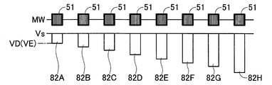
- the “negative bias voltage (V)” of the applied voltage table 55 shown in FIG. 10 is associated with the “order” in which one microwave pulse 51 is supplied, and the sheath layer
- the negative applied voltage values of the negative bias voltage pulses 82A, 82B, 82C,... Set so as to gradually increase the sheath thickness 42 in a predetermined range are stored.
- Each negative applied voltage is set to be a constant voltage from the initial voltage VD to the final voltage VE so that the negative applied voltage of each bias voltage pulse 82A, 82B, 82C,... Changes stepwise. ing.
- the CPU 31 executes the sub-process of “sheath thickness control process 1” in S22 of the “film formation process”, it is applied to the workpiece 8 via the negative voltage electrode 25 in S114.
- the absolute value of the negative applied voltage gradually increases with each application.
- the sheath thickness of the sheath layer 42 formed on the surface of the workpiece 8 gradually increases every time a negative applied voltage is applied, and a DLC film is formed.
- the film hardness in the DLC film 73 formed on the surface of the material 8 to be processed is similar to the film forming apparatus 71 according to the third embodiment.
- the distance from the outer side in the direction can be gradually increased, and the adhesion of the DLC film 73 to the workpiece 8 can be improved.
- the CPU 31 may increase the negative bias voltage applied to the material 8 to be processed, for example, every two pulses. That is, the negative applied voltage applied to the workpiece 8 may be increased for each of a plurality of pulses.
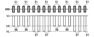
- a film forming apparatus 91 according to the fifth embodiment will be described with reference to FIG.
- the same reference numerals as those of the film forming apparatus 71 according to the third embodiment denote the same or corresponding parts as those of the film forming apparatus 71 according to the third embodiment.
- the schematic configuration of the film forming apparatus 91 according to the fifth embodiment is substantially the same as the film forming apparatus 71 according to the third embodiment.
- the “negative bias voltage (V)” of the applied voltage table 55 shown in FIG. 10 is associated with the “order” in which one microwave pulse 51 is supplied, and the sheath layer
- the sheath layer normal enlarged applied voltage which is the negative applied voltage of the negative bias voltage pulses 72A, 72B, 72C,... Set so as to gradually increase the sheath thickness of 42 in a predetermined range, is stored. Yes.
- An enlarged applied voltage VQ is stored.
- the application time T22 10 (microseconds)
- the negative sheath layer initial enlarged application voltage VQ is ⁇ 400 V (the sheath potential is ⁇ 430 V).
- the CPU 31 executes the sub-process of “Sheath thickness control process 1” in S24 of the “Film formation process”, so that the target is passed through the negative voltage electrode 25 in S114.
- the negative bias voltage pulse applied to the work material 8 is gradually applied after the sheath layer initial enlarged application voltage pulse 92 having the negative sheath layer initial enlarged application voltage VQ is applied for the application time T22 (seconds).
- the film hardness in the DLC film 73 formed on the surface of the work material 8 is the same as the film forming apparatus 71 according to the third embodiment.
- the distance from the outer side in the direction can be gradually increased, and the adhesion of the DLC film 73 to the workpiece 8 can be improved.
- the surface wave excitation plasma can be stably extended at a high speed along the surface of the material 8 to be processed, and the followability to the high-speed film formation by the MVP method can be further improved.
- FIGS. 1 to 13 the same reference numerals as those of the film forming apparatus 1 according to the first embodiment in FIGS. 1 to 13 denote the same or corresponding parts as those of the film forming apparatus 1 according to the first embodiment. It is shown.
- the schematic configuration of the film forming apparatus 95 according to the sixth embodiment is substantially the same as that of the film forming apparatus 1 according to the first embodiment.
- the “negative bias voltage (V)” of the applied voltage table 55 shown in FIG. 10 is associated with the “order” in which the microwave pulse 51 is supplied, and the negative voltage electrode 25.
- the negative applied voltage VK of the negative bias voltage pulse 96 applied to the negative voltage and the negative applied voltage VL having a larger absolute value than the negative applied voltage VK of the negative bias voltage pulse 97 applied to the negative voltage electrode 25 are
- the wave pulses 51 are stored alternately and repeatedly for a plurality of times, for example, every four times.
- the negative applied voltage VK ⁇ 200 V (sheath potential is ⁇ 230 V)
- the negative applied voltage VL ⁇ 400 V (sheath potential is ⁇ 430 V).
- the negative bias voltage pulse applied to the work material 8 includes a negative bias voltage pulse 96 of the negative applied voltage VK and a negative applied voltage every a plurality of times, for example, four times of supply of the microwave pulse 51.
- a negative bias voltage pulse 97 of VL is repeatedly applied alternately.
- the sheath thickness of the sheath layer 42 formed on the surface of the work material 8 is such that the sheath layer 42 having a small sheath thickness and the sheath thickness are supplied every plural times, for example, four times of the supply of the microwave pulse 51. Large sheath layers 42 are alternately and repeatedly formed, and a DLC film is formed on the surface of the workpiece 8.
- the high-hardness DLC films 99 formed by applying the negative bias voltage pulse 97 are alternately laminated with a predetermined film thickness.
- the DLC films 98 and 99 can be coated by alternately laminating the low-hardness DLC films 98 and the high-hardness DLC films 99 on the surface of the material 8 to be processed.
- the adhesion to the processing material 8 can be improved.
- the sheath thickness of the sheath layer 42 is gradually reduced within a predetermined range in association with the “order” in which one microwave pulse 51 is supplied.
- the absolute value of the negative applied voltage of the negative bias voltage pulses 82A, 82B, 82C,... May be set to be gradually reduced.
- the sheath thickness of the sheath layer 42 is set within a predetermined range in association with the “order” in which one microwave pulse 51 shown in FIG. 21 is supplied.
- the absolute value of the negative applied voltage of the negative bias voltage pulses 82A, 82A, 82B, 82B, 82C, 82C,... Set every 2 pulses is gradually decreased every 2 pulses so as to gradually decrease. You may make it set so that it may become.
- the film hardness in the DLC film 73 formed on the surface of the material to be processed 8 can be gradually lowered as it goes away in the film thickness direction, and the film hardness formed on the surface of the material to be processed 8 is formed.
- the familiarity with the contact member on which the DLC film 73 slides can be improved.
- the sheath thickness of the sheath layer 42 is gradually reduced within a predetermined range in association with the “order” in which one microwave pulse 51 is supplied.
- the absolute value of the negative applied voltage of the negative bias voltage pulses 72A, 72B, 72C,... May be set to be gradually reduced.
- the workpiece 8 is held by the holder 9, but may be configured to be directly supported by the microwave supply port 22.
Landscapes
- Chemical & Material Sciences (AREA)
- Engineering & Computer Science (AREA)
- Physics & Mathematics (AREA)
- Plasma & Fusion (AREA)
- Organic Chemistry (AREA)
- General Chemical & Material Sciences (AREA)
- Chemical Kinetics & Catalysis (AREA)
- Materials Engineering (AREA)
- Mechanical Engineering (AREA)
- Metallurgy (AREA)
- Analytical Chemistry (AREA)
- Spectroscopy & Molecular Physics (AREA)
- Electromagnetism (AREA)
- Inorganic Chemistry (AREA)
- Plasma Technology (AREA)
- Chemical Vapour Deposition (AREA)
Abstract
導電性を有する被加工材料の処理表面に沿ってプラズマを生成させるためのマイクロ波を供給するマイクロ波供給部と、前記被加工材料の処理表面に沿うシース層を拡大させる負のバイアス電圧を前記被加工材料に印加する負電圧印加部と、前記マイクロ波供給部と前記負電圧印加部とを制御する制御部と、を備え、前記マイクロ波供給部は、供給するマイクロ波を拡大された前記シース層へ伝搬させるマイクロ波供給口を有し、前記制御部は、前記マイクロ波の供給中に、前記シース層のシース厚さを変化させるように前記マイクロ波供給部と前記負電圧印加部とを制御する。
Description
本発明は、プラズマを用い、鋼材等の導電性を有する被加工材料の表面に皮膜を形成するための成膜装置、成膜方法及び成膜プログラムに関するものである。
従来より、プラズマを用い、鋼材等の導電性を有する被加工材料の表面に皮膜を形成するための成膜装置に関し種々提案されている。
例えば、上述した被加工材料の表面にダイヤモンドライクカーボン(以下、「DLC」という。)成膜処理する技術が特開2004-47207号公報等により知られている。
例えば、上述した被加工材料の表面にダイヤモンドライクカーボン(以下、「DLC」という。)成膜処理する技術が特開2004-47207号公報等により知られている。
この特開2004-47207号公報に開示された技術では、プラズマ生成装置がマイクロ波供給口である石英窓を通して処理容器内の被加工材料に向けマイクロ波を供給することにより、石英窓内面の周辺領域にプラズマが生成される。被加工材料は例えば棒状であり、石英窓内面から処理容器内に突出するように配置され、生成されたプラズマに覆われた被加工材料の石英窓内面の周辺部分にはシース層が生成される。続いて、マイクロ波の供給中に、プラズマ生成装置が被加工材料へ負のバイアス電圧を印加する。
この結果、被加工材料の表面に生成されたシース層は被加工材料の表面に沿って拡大する。また同時に、供給されたマイクロ波は、この拡大されたシース層に沿って高エネルギー密度の表面波として伝搬する。このとき、高エネルギー密度の表面波により石英窓内面周辺から離れた被加工材料の表面にもプラズマが生成され、シース層も生成される。この新たに生成されたシース層も負のバイアス電圧によって拡大され、この拡大されたシース層に沿ってマイクロ波が高エネルギー密度の表面波としてさらに伝搬する。これにより、被加工材料の石英窓周辺から離れた部分へ、すなわち、被加工材料の石英窓側の一端から処理容器内に突出した他端へとプラズマが伸長する。この結果、原料ガスが表面波によってプラズマ励起されて高密度プラズマとなり、被加工材料の表面全体にDLC成膜処理される。
しかしながら、特開2004-47207号公報に開示された技術では、被加工材料に印加される負のバイアス電圧は一定である。そのため、シース層内を高エネルギー密度の表面波として伝搬するマイクロ波の一部が、被加工材料のマイクロ波の供給側とは反対側において反射され、被加工材料のマイクロ波伝搬方向に沿った定在波となる。その結果、表面波によってプラズマ励起される高密度プラズマに定在波分布に応じたプラズマ密度分布が生じて、皮膜の膜厚、膜硬度等の膜特性が不均一になるという問題がある。
そこで、本発明は、上述した問題点を解決するためになされたものであり、被加工材料の表面に形成された皮膜の膜厚、膜硬度等の膜特性を均一化することができる成膜装置、成膜方法及び成膜プログラムを提供することを目的とする。
前記目的を達成するため本発明の成膜装置は、導電性を有する被加工材料の処理表面に沿ってプラズマを生成させるためのマイクロ波を供給するマイクロ波供給部と、前記被加工材料の処理表面に沿うシース層を拡大させる負のバイアス電圧を前記被加工材料に印加する負電圧印加部と、前記マイクロ波供給部と前記負電圧印加部とを制御する制御部と、を備え、前記マイクロ波供給部は、供給するマイクロ波を拡大された前記シース層へ伝搬させるマイクロ波供給口を有し、前記制御部は、前記マイクロ波の供給中に、前記シース層のシース厚さを変化させるように前記マイクロ波供給部と前記負電圧印加部とを制御することを特徴とする。
このような成膜装置では、マイクロ波供給部によるマイクロ波の供給中に、シース層を生成すると共に、シース層のシース厚さを変化させることによって、シース層内を高エネルギー密度の表面波として伝搬するマイクロ波によって生成される定在波の分布を変化させることができる。これにより、表面波によってプラズマ励起された原料ガスの高密度プラズマのプラズマ密度の分布を変化させることができ、被加工材料の表面に形成された皮膜の膜厚、膜硬度等の膜特性を均一化することができる。
また、前記本発明の成膜装置において、前記制御部は、前記マイクロ波供給部によるマイクロ波の供給中に、前記被加工材料に印加される前記負のバイアス電圧の電圧値を変化させて前記シース厚さを変化させるように前記負電圧印加部を駆動制御するようにしてもよい。
このような成膜装置では、マイクロ波供給部によるマイクロ波の供給中に、被加工材料に印加される負のバイアス電圧の電圧値を変化させてシース厚さを変化させるため、シース層のシース厚さを高速に変化させることができる。これにより、シース層内を高エネルギー密度の表面波として伝搬するマイクロ波によって生成される定在波の分布変化を高速に行い、高速成膜への追従性の向上を図ることができる。
また、前記本発明の成膜装置において、前記制御部は、前記マイクロ波供給部によるマイクロ波の供給中に、前記被加工材料に電圧値の異なる複数種類のパルス状の負のバイアス電圧を順次印加して、前記シース厚さの拡大と減縮を繰り返すように前記負電圧印加部を駆動制御するようにしてもよい。
このような成膜装置では、マイクロ波供給部によるマイクロ波の供給中に、被加工材料に電圧値の異なる複数種類のパルス状の負のバイアス電圧を順次印加して、シース厚さの拡大と減縮を繰り返す。これにより、シース層内を高エネルギー密度の表面波として伝搬するマイクロ波によって生成される定在波の分布変化を均一化することができ、被加工材料の表面に形成された皮膜の膜厚、膜硬度等の膜特性の更なる均一化を図ることができる。
また、前記本発明の成膜装置において、前記制御部は、前記マイクロ波供給部によるマイクロ波の供給中に、前記被加工材料に印加される前記負のバイアス電圧の電圧値を1パルス毎又は複数パルス毎に徐々に変化させるように前記負電圧印加部を駆動制御するようにしてもよい。
このような成膜装置では、マイクロ波供給部によるマイクロ波の供給中に、被加工材料に印加される負のバイアス電圧の電圧値を1パルス毎又は複数パルス毎に徐々に変化させることによって、被加工材料の表面に所望の膜特性を有する皮膜を形成することができる。
例えば、負のバイアス電圧の電圧値を1パルス毎又は複数パルス毎に徐々に大きくした場合には、被加工材料の表面に形成される皮膜の硬度が徐々に大きくなり、皮膜の被加工材料への密着性の向上を図ることできる。また、負のバイアス電圧の電圧値を1パルス毎又は複数パルス毎に徐々に小さくした場合には、被加工材料の表面に形成される皮膜の硬度が徐々に小さくなり、摺動する接触部材へのなじみの向上を図ることができる。
また、前記本発明の成膜装置において、前記制御部は、前記被加工材料に前記負のバイアス電圧を印加する負電圧電極の形状が、前記シース層内を前記マイクロ波が表面波として伝搬する伝搬方向において、不連続部を形成する場合には、前記シース層内を伝搬する前記表面波の波長に基づいて前記負のバイアス電圧の電圧値を変化させるようにしてもよい。
このような成膜装置では、被加工材料に負のバイアス電圧を印加する負電圧電極の形状が、シース層内をマイクロ波が伝搬する伝搬方向において、不連続部を形成する場合には、シース層内を伝搬する表面波の波長に基づいて負のバイアス電圧の電圧値を変化させる。これにより、定在波の分布を変化させることが可能となり、被加工材料の表面に形成された皮膜の膜厚、膜硬度等の膜特性の更なる均一化を図ることができる。
更に、前記本発明の成膜装置において、前記マイクロ波供給部は、前記被加工材料にパルス状のマイクロ波を供給し、前記制御部は、前記マイクロ波の1パルス内において、前記負のバイアス電圧の電圧値を変化させて前記シース厚さを変化させるように前記負電圧印加部を駆動制御するようにしてもよい。
このような成膜装置では、パルス状のマイクロ波の1パルス内において、負のバイアス電圧の電圧値を変化させてシース層のシース厚さを変化させることによって、被加工材料の表面に沿って生成されたシース層によりプラズマを高速で伸長させることができる。また、プラズマが安定した場合には、所定シース厚さで被加工材料の表面に皮膜を形成することができる。
また、本発明の成膜方法は、導電性を有する被加工材料にマイクロ波供給口を介してマイクロ波を供給するマイクロ波供給部と、負のバイアス電圧を前記被加工材料に印加する負電圧印加部と、制御部と、を備えた成膜装置で実行される成膜方法であって、前記制御部が実行する、前記マイクロ波供給部を介して前記被加工材料の処理表面に沿ってプラズマを生成させるためのマイクロ波を供給するマイクロ波供給工程と、前記負電圧印加部を介して前記被加工材料の処理表面に沿うシース層を拡大させる負のバイアス電圧を前記被加工材料に印加する負電圧印加工程と、前記マイクロ波供給口を介して供給されるマイクロ波を拡大された前記シース層へ伝搬させるマイクロ波伝搬工程と、前記マイクロ波供給部と前記負電圧印加部とを制御する制御工程と、を備え、前記制御部は、前記制御工程において、前記マイクロ波の供給中に、前記シース層のシース厚さを変化させるように前記マイクロ波供給部と前記負電圧印加部とを制御することを特徴とする。
このような成膜方法では、マイクロ波供給部によるマイクロ波の供給中に、シース層を生成すると共に、シース層のシース厚さを変化させることによって、シース層内を高エネルギー密度の表面波として伝搬するマイクロ波によって生成される定在波の分布を変化させることができる。これにより、表面波によってプラズマ励起された原料ガスの高密度プラズマのプラズマ密度の分布を変化させることができ、被加工材料の表面に形成された皮膜の膜厚、膜硬度等の膜特性を均一化することができる。
また、本発明の成膜プログラムは、導電性を有する被加工材料にマイクロ波供給口を介してマイクロ波を供給するマイクロ波供給部と、負のバイアス電圧を前記被加工材料に印加する負電圧印加部と、を備えた成膜装置を制御するコンピュータに、前記マイクロ波供給部を介して前記被加工材料の処理表面に沿ってプラズマを生成させるためのマイクロ波を供給するマイクロ波供給工程と、前記負電圧印加部を介して前記被加工材料の処理表面に沿うシース層を拡大させる負のバイアス電圧を前記被加工材料に印加する負電圧印加工程と、前記マイクロ波供給口を介して供給されるマイクロ波を拡大された前記シース層へ伝搬させるマイクロ波伝搬工程と、前記マイクロ波供給部と前記負電圧印加部とを制御する制御工程を実行させ、前記制御工程において、前記マイクロ波の供給中に、前記シース層のシース厚さを変化させるように前記マイクロ波供給部と前記負電圧印加部とを制御するように実行させるためのプログラムである。
このような成膜プログラムでは、コンピュータは当該プログラムを読み込むことによって、マイクロ波供給部によるマイクロ波の供給中に、シース層を生成すると共に、シース層のシース厚さを変化させることによって、シース層内を高エネルギー密度の表面波として伝搬するマイクロ波によって生成される定在波の分布を変化させることができる。これにより、コンピュータは、表面波によってプラズマ励起された原料ガスの高密度プラズマのプラズマ密度の分布を変化させることができ、被加工材料の表面に形成された皮膜の膜厚、膜硬度等の膜特性を均一化することができる。
以下、本発明に係る成膜装置について具体化した第1実施形態乃至第7実施形態に基づき図面を参照しつつ詳細に説明する。先ず、第1実施形態に係る成膜装置1の概略構成について図1及び図2に基づいて説明する。
[第1実施形態]
図1及び図2に示すように、第1実施形態に係る成膜装置1は、処理容器2、真空ポンプ3、ガス供給部5、及び制御部6等から構成されている。処理容器2は、ステンレス等の金属製であって、気密構造の処理容器である。真空ポンプ3は、圧力調整バルブ7を介して処理容器2の内部を真空排気可能なポンプである。処理容器2の内部には、成膜対象である導電性を有する被加工材料8が、ステンレス等で形成された導電性を有する保持具9により保持されている。
図1及び図2に示すように、第1実施形態に係る成膜装置1は、処理容器2、真空ポンプ3、ガス供給部5、及び制御部6等から構成されている。処理容器2は、ステンレス等の金属製であって、気密構造の処理容器である。真空ポンプ3は、圧力調整バルブ7を介して処理容器2の内部を真空排気可能なポンプである。処理容器2の内部には、成膜対象である導電性を有する被加工材料8が、ステンレス等で形成された導電性を有する保持具9により保持されている。
被加工材料8の材質は、導電性を有していれば、特に限定されるものではないが、第1実施形態では低温焼戻し鋼である。ここで低温焼戻し鋼とは、JIS G4051(機械構造用炭素鋼鋼材)、G4401(炭素工具鋼鋼材)、G44-4(合金工具用鋼材)、又はマルエージング鋼材などの材料である。被加工材料は、低温焼戻し鋼以外にも、セラミック、または樹脂に導電性の材料がコーティングされているものでもよい。
ガス供給部5は、処理容器2の内部に成膜用の原料ガスと不活性ガスとを供給する。具体的には、He、Ne、Ar、Kr、またはXeなどの不活性ガスとCH4、C2H2、又はTMS(テトラメチルシラン)等の原料ガスとが供給される。第1実施形態では、C2H2、CH4、およびTMSの原料ガスにより被加工材料8がDLC成膜処理されるとして説明する。
また、ガス供給部5から供給される原料ガス、および不活性ガスの流量、および圧力が後述するCPU31により制御されてもよいし、作業者により制御されてもよい。また、原料ガスは、アルキン、アルケン、アルカン、芳香族化合物などのCH結合を有する化合物、または炭素が含まれる化合物が含まれるガスであればよい。また、H2が原料ガスに含まれてもよい。
処理容器2の内部に保持された被加工材料8に対してDLC成膜処理を行うためのプラズマが発生される。このプラズマは、マイクロ波パルス制御部11、マイクロ波発振器12、マイクロ波電源13(図2参照)、負電圧電源15、及び負電圧パルス発生部16により発生される。第1実施形態では、特開2004-47207号公報に開示された方法(以下、「MVP法(Microwave Voltage coupled Plasma法)」という。)により表面波励起プラズマが発生されるとして説明する。以降の記載では、MVP法を説明する。
マイクロ波パルス制御部11は制御部6の指示に従い、パルス信号を発振し、この発振したパルス信号をマイクロ波発振器12へ供給する。マイクロ波発振器12は、マイクロ波パルス制御部11からのパルス信号に従って、マイクロ波パルスを発生する。マイクロ波電源13は、制御部6の指示従い、指示された出力で2.45GHzのマイクロ波を発振するマイクロ波発振器12へ電力を供給する。つまり、マイクロ波発振器12は、2.45GHzのマイクロ波をマイクロ波パルス制御部11からのパルス信号に従って、パルス状のマイクロ波パルスで後述するアイソレータ17に供給する。
そして、マイクロ波パルスは、マイクロ波発振器12からアイソレータ17、チューナー18、導波管19、導波管19から図示されない同軸導波管変換器を介して突設された同軸導波管21、及び石英などのマイクロ波を透過する誘電体等からなるマイクロ波供給口22を経由し、保持具9及び被加工材料8の処理表面に供給される。アイソレータ17は、マイクロ波の反射波がマイクロ波発振器12へ戻ることを防ぐものである。チューナー18は、マイクロ波の反射波が最小になるようにチューナー18前後のインピーダンスを整合するものである。
マイクロ波供給口22の上端面22Aを除く外周面は、ステンレス等の金属で形成された側面電極23で被覆されている。側面電極23は、処理容器2の内側面にネジ止め等によって固定され、電気的に処理容器2に接続されている。マイクロ波供給口22の中央には同軸導波管21の中心導体が延長されている。保持具9も中心導体の延長上にあり、マイクロ波供給口22内では中心導体となる。従って、マイクロ波供給口22の中心導体と側面電極23とで同軸導波管として機能する。
このため、マイクロ波供給口22に供給されたマイクロ波パルスによって、保持具9が設けられた上端面22A付近にマイクロ波が伝搬してプラズマが生成される。また、被加工材料8の保持具9に対して反対側の部分は、マイクロ波供給口22に対して処理容器2の内側に向かって突出するように配置され、負のバイアス電圧パルスを印加するための負電圧電極25が電気的に接続されている。
マイクロ波供給口22の中心導体は真空を保持するため、途中で分断されているが、誘電体とのろう付け等で真空が保持されれば、貫通していてもよい。被加工材料8は、例えば棒状であり、マイクロ波供給口22の中心導体の延長線上に保持される。保持具9の替わりに被加工材料8の一部がマイクロ波供給口22内の中心導体となるように保持されてもよい。
負電圧電源15は、制御部6の指示に従い、負電圧パルス発生部16に負のバイアス電圧を供給する。負電圧パルス発生部16は、負電圧電源15から供給された負のバイアス電圧をパルス化する。このパルス化の処理は、負電圧パルス発生部16が制御部6の指示に従い、負のバイアス電圧パルスの大きさ、周期、及び、デューティ比を制御する処理である。このパルス状の負のバイアス電圧である負のバイアス電圧パルスが、処理容器2の内部に保持された被加工材料8に負電圧電極25を介して印加される。
即ち、被加工材料8が、金属基材の場合、またはセラミック、または樹脂に導電性の材料がコーティングされた場合であっても、被加工材料8の少なくとも処理表面全域に負のバイアス電圧パルスが印加される。また、保持具9の表面全域にも被加工材料8を介して負のバイアス電圧パルスが印加される。
図7に示すように、発生されたマイクロ波パルス、および負のバイアス電圧パルスの少なくとも一部が同一時間に印加されるように制御されることにより表面波励起プラズマ45が発生される。マイクロ波は2.45GHzに限らず、0.3GHz~50GHzの周波数であればよい。負電圧電源15、および負電圧パルス発生部16が本発明の負電圧印加部の一例である。
マイクロ波制御部11、マイクロ波発振器12、マイクロ波電源13、アイソレータ17、チューナー18、導波管19、同軸導波管21およびマイクロ波供給口22が本発明のマイクロ波供給部の一例である。尚、成膜装置1は負電圧電源15、および負電圧パルス発生部16を備えたが、正電圧電源、および正電圧パルス発生部を備えても良いし、負電圧パルス発生部16の代わりに、パルス状の負のバイアス電圧でなく、連続する負のバイアス電圧を印加する負電圧発生部を備えてもよい。
成膜装置1が、連続する負のバイアス電圧を印加する負電圧発生部を備える場合、正電圧パルス発生部も備えるのが望ましい。連続する負のバイアス電圧が、被加工材料8に印加され続けると、アーキングが発生しやすくなる。このアーキングの発生を低減するためにパルス状の正のバイアス電圧が、負のバイアス電圧が印加される期間の内、負のバイアス電圧が印加される期間の数パーセントの期間において印加されるのが望ましい。
図2に示すように、制御部6は、負電圧電源15とマイクロ波電源13に制御信号を出力してマイクロ波パルスの印加電力と負電圧パルスの印加電圧を制御する。制御部6は、負電圧パルス発生部16及びマイクロ波パルス制御部11に制御信号を出力することによって、パルス状の負のバイアス電圧パルスの印加タイミング、供給電圧、及びマイクロ波発振器12から発生されるマイクロ波パルスの供給タイミング、及び供給電力を制御する。
また、制御部6は、ガス供給部5に流量制御信号を出力して原料ガス及び不活性ガスの供給を制御する。制御部6は、処理容器2に取り付けられた真空計26から入力される処理容器2内の圧力を表す圧力信号に基づいて、制御信号を圧力調整バルブ7に出力して、処理容器2内の圧力を制御する。
制御部6は、CPU31、RAM32、ROM33、ハードディスクドライブ(以下、「HDD」という。)34、時間を計測するタイマ35、図11に示す「シース厚さ制御処理1」のサブ処理の処理時間を計測する終了判定用タイマ36等を備え、コンピュータから構成される。CPU31は、RAM32等の揮発性記憶装置に種々の情報を一時記憶し、図11に示す成膜処理等のプログラムを実行して、成膜装置1の全体の制御を行う。ROM33とHDD34は、不揮発性記憶装置であり、図11に示す成膜処理等のプログラム、図9に示すマイクロ波パルスと負のバイアス電圧パルスの印加タイミング、図10に示す印加電圧テーブル55等を記憶している。
更に、制御部6には、圧力調整バルブ7、真空計26、負電圧電源15、負電圧パルス発生部16、マイクロ波パルス制御部11、ガス供給部5、及びマイクロ波電源13が電気的に接続されている。尚、図11に示す成膜処理のプログラムは、図示しないドライバによりCD-ROM、またはDVD-ROMなどの記憶媒体から読み込まれてもよいし、図示しないインターネットなどのネットワークからダウンロードされてもよい。
[表面波励起プラズマの説明]
通常、表面波励起プラズマを発生させる場合、ある程度以上の電子(イオン)密度におけるプラズマと、これに接する誘電体との界面に沿ってマイクロ波が供給される。供給されたマイクロ波は、この界面に電磁波のエネルギーが集中した状態で表面波として伝播される。その結果、界面に接するプラズマは高エネルギー密度の表面波によって励起され、さらに増幅される。これにより高密度プラズマが生成されて維持される。ただし、この誘電体を導電性材料に換えた場合、導電性材料は表面波の導波路としては機能せず、好ましい表面波の伝播及びプラズマ励起を生ずることはできない。
通常、表面波励起プラズマを発生させる場合、ある程度以上の電子(イオン)密度におけるプラズマと、これに接する誘電体との界面に沿ってマイクロ波が供給される。供給されたマイクロ波は、この界面に電磁波のエネルギーが集中した状態で表面波として伝播される。その結果、界面に接するプラズマは高エネルギー密度の表面波によって励起され、さらに増幅される。これにより高密度プラズマが生成されて維持される。ただし、この誘電体を導電性材料に換えた場合、導電性材料は表面波の導波路としては機能せず、好ましい表面波の伝播及びプラズマ励起を生ずることはできない。
一方、プラズマに接する物体の表面近傍には、本質的に単一極性の荷電粒子層、いわゆるシース層が形成される。物体が、負のバイアス電圧を加えた導電性を有する被加工材料8の場合、シース層とは電子密度が低い層、すなわち、正極性であって、マイクロ波の周波数帯においてはほぼ比誘電率ε≒1の層である。このため、印加する負のバイアス電圧の絶対値を例えば-100Vの絶対値より大きくすることによりシース層のシース厚さを厚くできる。すなわちシース層が拡大する。このシース層が、プラズマとプラズマに接する物体との界面に表面波を伝播させる誘電体として作用する。
従って、被加工材料8を保持する保持具9の一端に近接して配置されたマイクロ波供給口22からマイクロ波が供給され、かつ被加工材料8及び保持具9に負のバイアス電圧が印加されると、マイクロ波はシース層とプラズマとの界面に沿って表面波として伝搬する。この結果、被加工材料8及び保持具9の表面に沿って表面波に基づく高密度励起プラズマが発生する。この高密度励起プラズマが、上述した表面波励起プラズマ45である。
このような被加工材料8の表面の近傍での表面波励起による高密度プラズマの電子密度は1011~1012cm-3に達する。このMVP法を用いたプラズマCVDによりDLC成膜処理される場合は、通常の負のバイアス電圧エネルギーのプラズマCVDによりDLC成膜処理される場合よりも1桁から2桁高い成膜速度3~30(ナノm/秒)が得られる。この結果、MVP法によるプラズマCVDの成膜時間は通常のプラズマCVDの成膜時間の1/10~1/100となる。
ここで、プラズマの電子密度が1012cm-3における、被加工材料8の表面に形成されたシース層のシース厚さとシース層を伝搬する表面波の波長との関係について図3に基づいて説明する。尚、被加工材料8は、直径10mmの円柱状に形成されている。
図3に示すように、例えば、シース厚さ約0.4mmのときの表面波の波長は、約30mmである。また、シース厚さ約0.6mmのときの表面波の波長は、約39mmである。また、シース厚さ約1.0mmのときの表面波の波長は、約52mmである。従って、シース層のシース厚さが厚くなるに従って、表面波の波長は長くなる。つまり、シース層のシース厚さを大きくすることによって、表面波の波長を長くすることができ、シース層のシース厚さを小さくすることによって、表面波の波長を短くすることができる。
次に、シース層のシース厚さが1mmにおける、プラズマの電子密度と表面波の波長との関係について図4に基づいて説明する。尚、黒丸印は、被加工材料8が直径1mmの円柱の時のデータを表している。黒四角印は、被加工材料8が直径10mmの円柱の時のデータを表している。
図4に示すように、例えば、プラズマの電子密度が2×1011cm-3の時には、被加工材料8が直径1mmの場合の表面波の波長は、約39mmであり、被加工材料8が直径10mmの場合の表面波の波長は、約19mmである。また、プラズマの電子密度が約1012cm-3の時には、被加工材料8が直径1mmの場合の表面波の波長は、約73mmであり、被加工材料8が直径10mmの場合の表面波の波長は、約52mmである。従って、プラズマの電子密度が高くなるに従って、表面波の波長は長くなる。つまり、マイクロ波の出力を大きくしてプラズマの電子密度を上昇させることによって、表面波の波長を長くすることができ、マイクロ波の出力を小さくしてプラズマの電子密度を低下させることによって、表面波の波長を短くすることができる。
次に、負のバイアス電圧を一定電圧にしたときにおける、プラズマの電子密度とシース層のシース厚さとの関係について図5に基づいて説明する。尚、負のバイアス電圧は、0V、-200V、-400Vとし、プラズマ電位を+30Vとした。従って、プラズマ電位に対する被加工材料8の電位であるシース電位が約-30V、約-230V、約-430Vのそれぞれについてプラズマの電子密度とシース層のシース厚さとを解析した。
図5に示すように、例えば、プラズマの電子密度が5×1011cm-3では、負のバイアス電圧が-30Vの時のシース層のシース厚さは、約0.1mmであり、負のバイアス電圧が-230Vの時のシース層のシース厚さは、約0.5mmであり、負のバイアス電圧が-430Vの時のシース層のシース厚さは、約0.9mmである。また、プラズマの電子密度が1012cm-3では、負のバイアス電圧が-30Vの時のシース層のシース厚さは、約0.06mmであり、負のバイアス電圧が-230Vの時のシース層のシース厚さは、約0.4mmであり、負のバイアス電圧が-430Vの時のシース層のシース厚さは、約0.6mmである。
従って、プラズマの電子密度が一定の場合には、負のバイアス電圧が大きくなるに従って、シース層のシース厚さは大きくなる。つまり、マイクロ波パルスの出力電力をほぼ一定にしてプラズマの電子密度をほぼ一定にした場合には、負のバイアス電圧を大きくすることによって、シース層のシース厚さを大きくすることができ、負のバイアス電圧を小さくすることによって、シース層のシース厚さを小さくすることができる。
[表面波の定在波分布]
次に、表面波の定在波分布について図3、図6乃至図8に基づいて説明する。
図6(A)に示すように、被加工材料8の先端部と負電圧電極25との接続部分において、マイクロ波の供給方向である図6(A)中の上下方向において、不連続な形状の不連続部41が形成されている場合には、不連続部41の周辺の表面に形成されるシース層42が不連続な形状になる。そのため、シース層42内を表面波として伝搬するマイクロ波は、この不連続部41の周辺に形成されたシース層42の不連続な部分で反射され、マイクロ波供給口22の上端面22Aから供給されるマイクロ波による表面波と干渉して、定在波を生成する。
次に、表面波の定在波分布について図3、図6乃至図8に基づいて説明する。
図6(A)に示すように、被加工材料8の先端部と負電圧電極25との接続部分において、マイクロ波の供給方向である図6(A)中の上下方向において、不連続な形状の不連続部41が形成されている場合には、不連続部41の周辺の表面に形成されるシース層42が不連続な形状になる。そのため、シース層42内を表面波として伝搬するマイクロ波は、この不連続部41の周辺に形成されたシース層42の不連続な部分で反射され、マイクロ波供給口22の上端面22Aから供給されるマイクロ波による表面波と干渉して、定在波を生成する。
例えば、図7(A)に模式的に示すように、シース層42のマイクロ波の伝搬方向に対して直交する方向のシース厚さが小さい場合には、図3に示すようにシース層42内を伝搬する表面波の波長は短くなるため、不連続部41で反射された表面波は、シース厚さ、プラズマの電子密度、及び被加工材料8の直径で定まる波長で定在波43を生成し、表面波励起プラズマ45が定在波43の1/2周期で密度分布する。そのため、表面波励起プラズマ45のプラズマ密度分布は、被加工材料8のマイクロ波の供給方向にプラズマ密度が低い節がいくつか発生し、各節の間にプラズマ密度が極大になる極大部が発生する。
また、例えば、図7(B)に模式的に示すように、シース層42のシース厚さが大きい場合には、図3に示すようにシース層42内を伝搬する表面波の波長は長くなる。このため、図7(A)に示す表面波よりも長い波長の表面波が、不連続部41で反射されるので生成される定在波44の波長も長くなり、表面波励起プラズマ45が定在波46の1/2
周期で密度波分布する。そのため、表面波励起プラズマ45のプラズマ密度分布は、図7(A)に示すプラズマ密度の節よりも少ない数のプラズマ密度が低い節が発生し、各節の間とマイクロ波供給口22の上端面22A近傍にプラズマ密度が極大になる極大部が発生する。
周期で密度波分布する。そのため、表面波励起プラズマ45のプラズマ密度分布は、図7(A)に示すプラズマ密度の節よりも少ない数のプラズマ密度が低い節が発生し、各節の間とマイクロ波供給口22の上端面22A近傍にプラズマ密度が極大になる極大部が発生する。
図7(A)、及び図7(B)に示すように、成膜中に、プラズマ密度が極大になる位置とプラズマ密度が極小になる位置とが固定されると、成膜終了後の被加工材料8の処理表面に膜厚、膜硬度等の膜特性が不均一となるDLC膜が成膜されてしまう。従って、成膜中に、プラズマ密度を均一化するため、プラズマ密度が極大になる位置とプラズマ密度が極小になる位置とを変動させてDLC成膜処理されるのが望ましい。
ここで、上記図3に示すように、プラズマの電子密度が1012cm-3において、2.45GHzのマイクロ波で励起されるシース厚さ約0.4mmのときの表面波の波長は、約30mmである。また、図5に示すように、このときの負のバイアス電圧は、約-200V(シース電位は、-230V)である。一方、表面波の波長を例えば1/4波長だけ長くして約37.5mmとするには、図5から負のバイアス電圧は、約-358V(シース電位は、-388V)で、図3に示すように、シース厚さは、約0.57mmにとなる。
従って、図7に示すように、プラズマの電子密度が1012cm-3において、負のバイアス電圧を約-200Vから約-358Vの間で変化させて、シース層42のシース厚さを約0.4mmと約0.57mmの間で変化させる。これにより、図8に示すように、不連続部41で反射された表面波によって生成される定在波は、表面波の波長が約30mmのときの定在波47と、表面波の波長が約37.5mmのときの定在波48との間で変化する。従って、表面波励起プラズマ45のプラズマ密度分布が、定在波47と定在波48との間で変化するため、成膜中に、プラズマ密度が極大になる位置とプラズマ密度が極小になる位置とが変動する。よって、被加工材料8の処理表面に形成されるDLC膜の膜厚や膜硬度等の膜特性の均一化を図ることができる。
また、図8において、縦軸は、相対的な定在波強度を示し、横軸は、不連続部41からの距離を示す。図8に示すように、表面波波長を約30mmから約37.5mmまでの間で変化させた場合には、表面波励起プラズマ45のプラズマ密度分布は、各定在波47、48の1/2周期で密度波分布する。そのため、定在波47によって生成されるプラズマ密度が極大になる各極大部の不連続部41からの距離は、約7.5mm、約22.5mm、約37.5mm、約52.5mm、約67.5mm・・・の位置に発生している。
また、定在波48によって生成されるプラズマ密度が極大になる各極大部の不連続部41からの距離は、約10mm、約30mm、約50mm、約70mm、約90mm・・・の位置に発生している。従って、表面波励起プラズマ45のプラズマ密度分布の各極大部の移動量は、不連続部41から離れるに従ってL1=約2.5mm、L2=約7.5mm、L3=約12.5mm、L4=約17.5mm、L5=約22.5mm、・・・となる。つまり、定在波47と定在波48との間でのプラズマ密度が極大になる位置、又は、プラズマ密度が極小になる位置の各移動量L1、L2、L3・・・は、不連続部41から離れるに従って大きくなっている。
従って、図6(B)に示すように、被加工材料8の先端部と負電圧電極25との間に、被加工材料8と連続な形状を有し、所定長さ(例えば、長さ約20mm~約60mmである。)のステンレス等で形成された導電性を有する連結部材49を設けるようにしてもよい。これにより、被加工材料8の処理表面におけるプラズマ密度分布の変化量、つまり、プラズマ密度が極大になる位置、又は、プラズマ密度が極小になる位置の移動量を更に大きくすることができ、被加工材料8の処理表面に形成されるDLC膜の膜厚や膜硬度等の膜特性の更なる均一化を図ることができる。
次に、マイクロ波パルスと負のバイアス電圧パルスの印加タイミングの一例について図9に基づいて説明する。
図9に示すように、マイクロ波パルス51の周期は、T3(秒)である。マイクロ波パルス51の1パルス毎の供給時間は、T2(秒)であり、第1実施形態では、T2はT3の約1/2に設定されている。また、負のバイアス電圧パルス52の周期は、マイクロ波パルス51の周期と同じ周期で、T3(秒)である。例えば、マイクロ波パルス51と負のバイアス電圧パルス52の周期は、T3=2(ミリ秒)である。
図9に示すように、マイクロ波パルス51の周期は、T3(秒)である。マイクロ波パルス51の1パルス毎の供給時間は、T2(秒)であり、第1実施形態では、T2はT3の約1/2に設定されている。また、負のバイアス電圧パルス52の周期は、マイクロ波パルス51の周期と同じ周期で、T3(秒)である。例えば、マイクロ波パルス51と負のバイアス電圧パルス52の周期は、T3=2(ミリ秒)である。
負のバイアス電圧パルス52の印加時間は、(T2-T1)(秒)であり、マイクロ波パルス51の供給時間T2(秒)の90%以上の時間に設定されている。そして、負のバイアス電圧パルス52の印加タイミングは、マイクロ波パルス51の供給開始タイミングよりもT1(秒)だけ遅延するように設定されている。つまり、マイクロ波パルス51が立ち上がり、電力が安定した後に、負のバイアス電圧パルス52が印加されるように設定されている。例えば、遅延時間T1=8(マイクロ秒)である。各時間T1、T2、T3(秒)を示す情報は、ROM33又はHDD34に記憶されている。
次に、ROM33又はHDD34に記憶されている印加電圧テーブル55の一例について図10に基づいて説明する。
図10に示すように、印加電圧テーブル55は、「順番」と、「マイクロ波出力(kW)」と、「負のバイアス電圧(V)」とから構成されている。この「順番」には、マイクロ波パルスを供給する順番「1」~「M」(回目)が記憶されている。
図10に示すように、印加電圧テーブル55は、「順番」と、「マイクロ波出力(kW)」と、「負のバイアス電圧(V)」とから構成されている。この「順番」には、マイクロ波パルスを供給する順番「1」~「M」(回目)が記憶されている。
また、「マイクロ波出力(kW)」には、マイクロ波パルス51を供給する「順番」に対応づけて、2.45GHzのマイクロ波の出力が記憶されている。尚、第1実施形態では、ほぼ1(kW)で一定値である。また、「負のバイアス電圧(V)」には、マイクロ波パルス51を供給する「順番」に対応づけて、負電圧電極25に印加する負のバイアス電圧パルス52の負の印加電圧値が記憶されている。つまり、シース層42のシース厚さを所定範囲の間で変化させるように設定された負のバイアス電圧パルス52の負の印加電圧値が、マイクロ波パルス51を供給する「順番」に対応づけて記憶されている。
例えば、プラズマの電子密度が1012cm-3において、シース層42のシース厚さを約0.4mmから約0.57mmの間で変化させるように、負の印加電圧値を約-200Vから約-358Vの間で、一定サイクル又はランダムに変化させた負の印加電圧値が、マイクロ波パルス51を供給する「順番」に対応づけて記憶されている。
[成膜処理]
次に、上記のように構成された成膜装置1のCPU31が実行する処理であって、被加工材料8の処理表面にDLC膜を成膜する成膜処理について図11乃至図13に基づいて説明する。この成膜処理は、保持具9に保持された被加工材料8が処理容器2の内部にセットされた状態で、作業者による成膜処理開始の指示が、不図示の操作部に設けられた操作ボタンを介して成膜装置1の制御部6に入力されたことをCPU31が検知することにより実行される。
次に、上記のように構成された成膜装置1のCPU31が実行する処理であって、被加工材料8の処理表面にDLC膜を成膜する成膜処理について図11乃至図13に基づいて説明する。この成膜処理は、保持具9に保持された被加工材料8が処理容器2の内部にセットされた状態で、作業者による成膜処理開始の指示が、不図示の操作部に設けられた操作ボタンを介して成膜装置1の制御部6に入力されたことをCPU31が検知することにより実行される。
図11に示すように、先ず、ステップ(以下、Sと略記する)11において、CPU31は、ROM33又はHDD34から図9に示すマイクロ波パルス51の周期T3(秒)を示す情報、1パルス毎の供給時間T2(秒)を示す情報を読み出し、RAM32に記憶する。例えば、マイクロ波パルス51の周期T3は2(ミリ秒)であり、1パルス毎の供給時間T2は1(ミリ秒)である。また、印加電圧テーブル55、及び後述するイオンクリーニングパラメータもROM33又はHDD34から読み出し、RAM32に記憶する。
また、CPU31は、ROM33又はHDD34から図9に示す負のバイアス電圧パルス52の周期T3(秒)を示す情報、1パルス毎の印加時間(T2-T1)(秒)を示す情報、マイクロ波パルス51の供給開始タイミングからの遅延時間T1(秒)を示す情報を読み出し、RAM32に記憶する。例えば、負のバイアス電圧パルス52の周期T3は2(ミリ秒)であり、1パルス毎の印加時間(T2-T1)は992(マイクロ秒)であり、遅延時間T1は8(マイクロ秒)である。尚、遅延時間T1は、約5(マイクロ秒)~20(マイクロ秒)に設定されてもよい。また、各時間T1、T2、T3(秒)は、作業者が不図示の操作部を介して成膜装置1の制御部6に入力するようにしてもよい。
そして、S12において、CPU31は、所定のパラメータをROM33又はHDD34から読み出して、RAM32に記憶し、真空ポンプ3を起動させる。所定のパラメータは、イオンクリーニングパラメータ、ガス流量値等のパラメータである。これらのパラメータは、作業者により手動で設定されてもよいし、予めROM33又はHDD34に記憶されたパラメータに基づき、自動で設定されてもよい。イオンクリーニングパラメータは、後述するイオンクリーニング処理のパラメータである。
続いて、S13において、CPU31は、真空計26から入力される圧力信号に基づいて、処理容器2の内部が、所定の真空度(例えば、1.0Pa未満である。)になったか否かを判定する判定処理を実行する。この所定の真空度は、予めROM33又はHDD34に記憶されている。そして、処理容器2の内部が、所定の真空度に達していないと判定した場合には(S13:NO)、CPU31は、再度、S13の処理を実行する。
一方、処理容器2の内部が、所定の真空度(例えば、1.0Pa未満である。)に達したと判定した場合には(S13:YES)、CPU31は、S14の処理に移行する。S14において、CPU31は、イオンクリーニングパラメータである不活性ガスArのガス流量値(例えば、ガス流量200sccmである。)をRAM32から読み出し、ガス供給部5に対して読み出されたガス流量値で処理容器2内へ不活性ガスArの供給をするように指示する供給信号を出力する。つまり、不活性ガスArの供給が開始される。
その後、S15において、CPU31は、圧力調整バルブ7を介して処理容器2内の原料ガス及び不活性ガスを一定流量で排気するように設定し、処理容器2の内部が所定圧力になるように調整する。続いて、S16において、CPU31は、真空計26から入力される圧力信号に基づいて、処理容器2の内部が、所定の圧力に達したか否かを判定する判定処理を実行する。そして、処理容器2の内部が、所定の圧力に達していないと判定した場合には(S16:NO)、CPU31は、再度、S15以降の処理を実行する。
一方、処理容器2の内部が、所定の圧力に達したと判定した場合には(S16:YES)、CPU31は、S17の処理に移行する。S17において、CPU31は、イオンクリーニングパラメータに基づいてイオンクリーニングを開始する。このイオンクリーニングパラメータには、マイクロ波の出力電力(例えば、800W電力である。)、負のバイアス電圧パルスの印加電圧(例えば、-200Vである。)が含まれている。
具体的には、CPU31は、負のバイアス電圧パルスの印加電圧を負電圧電源15に送信する。CPU31は、マイクロ波の出力電力をマイクロ波電源13に送信する。CPU31は、S11で取得した負のバイアス電圧パルス52の周期T3(秒)、1パルス毎の印加時間(T2-T1)(秒)、及び、マイクロ波パルス51の供給開始タイミングからの遅延時間T1(秒)に基づいて、負のバイアス電圧パルス52のオン信号、及びオフ信号を負電圧パルス発生部16に送信する。CPU31は、S11で取得したマイクロ波パルス51の周期T3(秒)、1パルス毎の供給時間T2(秒)に基づいて、マイクロ波パルス51のオン信号、及びオフ信号をマイクロ波パルス制御部11に送信する。
この結果、負電圧電源15は、受信した印加電圧に従い、負電圧パルス発生部16に負の印加電圧を供給する。負電圧パルス発生部16は、供給された負の印加電圧と、周期T3(秒)毎に受信した負のバイアス電圧パルス52のオン信号、及びオフ信号により、マイクロ波パルスの供給開始からT1(秒)遅延して、負のバイアス電圧パルス52を、負電圧電極25を介して被加工材料8に(T2-T1)秒間、印加する。
また、マイクロ波電源13は、受信したマイクロ波の出力電力に従い、マイクロ波発振器12に電力を供給する。マイクロ波パルス制御部11は、受信したマイクロ波パルス51のオン信号、及びオフ信号に従い、周期T3(秒)毎に、供給時間T2(秒)間のパルス信号をマイクロ波発振器12に送信する。マイクロ波発振器12は、周期T3(秒)毎に、受信したパルス信号に従う供給時間T2(秒)のマイクロ波パルス51を、供給された電力に応じた2.45GHzのマイクロ波電力で、アイソレータ17、チューナー18、導波管19、同軸導波管21及びマイクロ波供給口22を介して保持具9及び被加工材料8に向け供給する。
これにより、図7に示すように、これら負のバイアス電圧パルス52により被加工材料8の表面に沿うシース層42が、マイクロ波の伝搬する伝搬方向に対して直交する方向に、つまり、図7の横方向に拡大され、シース層42内を伝搬するマイクロ波パルス51により不活性ガスArのプラズマが発生する。この発生された不活性ガスArのプラズマにより、被加工材料8の表面がイオンクリーニングされ、後述するDLC膜が形成されやすくなる。イオンクリーニングを開始すると、CPU31は、S18の処理に移行する。
S18において、CPU31は、イオンクリーニングを終了するか否かを判定する。この判定は、アーキング発生頻度が所定の頻度未満か否かにより判定される。所定の頻度は、ROM33又はHDD34に予め記憶されている。そして、アーキング発生頻度が所定の頻度以上であると判定した場合には(S18:NO)、CPU31は、再度S18の処理を実行する。
一方、アーキング発生頻度が所定の頻度未満であると判定した場合には(S18:YES)、CPU31は、S19の処理に移行する。尚、この終了判定は、イオンクリーニングパラメータとしてイオンクリーニング時間が設定され、CPU31は、イオンクリーニング開始からタイマ35で計測した時間がイオンクリーニング時間を経過したか否かで判定してもよい。
S19において、CPU31は、マイクロ波パルス制御部11にマイクロ波発振器12に送信しているパルス信号を停止するように指示する停止信号を送信する。これにより、マイクロ波発振器12は、パルス信号を受信しないため、マイクロ波パルス51の出力を停止する。また、CPU31は、負電圧パルス発生部16に負のバイアス電圧パルス52の印加を停止するように指示する停止信号を送信する。これにより、負電圧パルス発生部16は、被加工材料8への負のバイアス電圧パルス52の印加を停止する。
続いて、S20において、CPU31は、ROM33又はHDD34から原料ガス及び不活性ガスを供給するそれぞれのガス流量値を読み出し、ガス供給部5に流量制御指示として送信した後、S21の処理に移行する。これにより、ガス供給部5は、流量制御指示に従い、原料ガス及び不活性ガスを処理容器2の内部に供給する。尚、原料ガス及び不活性ガスを供給するそれぞれのガス流量値は、予めROM33又はHDD34に記憶されている。例えば、不活性ガスArは、40sccmである。CH4は、200sccmである。C2H2は、0sccmである。TMSは、20sccmである。
S21において、CPU31は、圧力調整バルブ7を介して処理容器2内の原料ガス及び不活性ガスを一定流量で排気するように設定し、処理容器2の内部が所定圧力になるように調整する。続いて、S22において、CPU31は、真空計26から入力される圧力信号に基づいて、処理容器2の内部が、所定の圧力に達したか否か、つまり、原料ガス及び不活性ガスの流量が安定したか否かを判定する判定処理を実行する。そして、処理容器2の内部が、所定の圧力に達していないと判定した場合には(S22:NO)、CPU31は、再度、S21以降の処理を実行する。
一方、処理容器2の内部が、所定の圧力に達したと判定した場合には(S22:YES)、CPU31は、S23において、CPU31は、RAM32から回数カウンタのカウント値Nを読み出し、このカウント値Nに「1」を代入して再度RAM32に記憶する。つまり、CPU31は、回数カウンタのカウント値を初期化する。同時に、CPU31は、終了判定用タイマ36の計測時間を「0」にリセットした後、処理時間の計測を開始させる。
続いて、S24において、CPU31は、後述のマイクロ波パルス51の1パルス毎にシース厚さを変化させる「シース厚さ制御処理1」である図12に示すサブ処理を実行した後、S25の処理に移行する。S25において、CPU31は、被加工材料8の表面にDLC膜を成膜する成膜処理が終了したか否かを判定する判定処理を実行する。具体的には、CPU31は、ROM33又はHDD34からS24において実行する「シース厚さ制御処理1」のサブ処理の処理時間を示す情報を読み出して、終了判定用タイマ36が処理時間に達したか否かを判定する判定処理を実行する。S24において実行する「シース厚さ制御処理1」のサブ処理の処理時間は、作業者により手動で設定されてもよいし、予めROM33又はHDD34に記憶されたパラメータに基づき、自動で設定されてもよい。
そして、被加工材料8の表面にDLC膜を成膜する成膜処理が終了していないと判定した場合、つまり、終了判定用タイマ36の計測時間がS24において実行するサブ処理の処理時間に達していないと判定した場合には(S25:NO)、CPU31は、再度、S24以降の処理を実行する。一方、被加工材料8の表面にDLC膜を成膜する成膜処理が終了したと判定した場合、つまり、終了判定用タイマ36の計測時間がS24において実行するサブ処理の処理時間に達したと判定した場合には(S25:YES)、CPU31は、S26の処理に移行する。
S26において、CPU31は、ガス供給部5に原料ガス及び不活性ガスの供給を停止するように指示する供給停止信号を送信する。また、CPU31は、圧力調整バルブ7へ排気を全開にするように指示する排気信号を送信する。これにより、ガス供給部5は、供給停止信号に従い、処理容器2の内部への原料ガス及び不活性ガスの供給を停止する。圧力調整バルブ7は、全開となり処理容器2内に残留している原料ガス及び不活性ガスを真空ポンプ3ですみやかに排気する。その後、CPU31は、処理を終了する。
[シース厚さ制御処理1]
次に、上記S24でCPU31が実行する「シース厚さ制御処理1」であるサブ処理について図12及び図13に基づいて説明する。
図12に示すように、先ず、S111において、CPU31は、タイマ35の計測時間を「0」にリセットし、成膜時間の計測を開始する。そして、S112において、CPU31は、回数カウンタのカウント値Nを、図10に示す印加電圧テーブル55の「順番」とし、この「順番」に対応づけられた「マイクロ波出力(kW)」を印加電圧テーブル55から読み出す。
次に、上記S24でCPU31が実行する「シース厚さ制御処理1」であるサブ処理について図12及び図13に基づいて説明する。
図12に示すように、先ず、S111において、CPU31は、タイマ35の計測時間を「0」にリセットし、成膜時間の計測を開始する。そして、S112において、CPU31は、回数カウンタのカウント値Nを、図10に示す印加電圧テーブル55の「順番」とし、この「順番」に対応づけられた「マイクロ波出力(kW)」を印加電圧テーブル55から読み出す。
そして、CPU31は、このマイクロ波の出力電力をマイクロ波電源13に送信する。CPU31は、マイクロ波パルスオン信号をマイクロ波パルス制御部11に送信する。この結果、マイクロ波電源13は、受信したマイクロ波の出力電力に従い、マイクロ波発振器12に電力を供給する、即ち、マイクロ波発振器12におけるマグネトロンに印加される印加電圧やアノード電流を供給する。マイクロ波パルス制御部11は、受信した供給時間T2(秒)を示す情報に従い、後述するS116の処理と合わせて供給時間T2(秒)間となるパルス信号をマイクロ波発振器12に向け送信開始する。
マイクロ波発振器12は、供給された電力で、供給時間T2(秒)の2.45GHzのマイクロ波パルス51を、アイソレータ17、チューナー18、導波管19、同軸導波管21及びマイクロ波供給口22を介して保持具9及び被加工材料8へ向け供給開始する。
続いて、S113において、CPU31は、タイマ35の計測時間が遅延時間T1(秒)になったか否か、つまり、負のバイアス電圧パルス52の印加タイミングになったか否かを判定する判定処理を実行する。そして、タイマ35の計測時間が遅延時間T1(秒)に達していないと判定した場合には(S113:NO)、CPU31は、再度S113の処理を実行する。
一方、タイマ35の計測時間が遅延時間T1(秒)に達したと判定した場合には(S113:YES)、CPU31は、S114の処理に移行する。S114において、CPU31は、回数カウンタのカウント値Nを図10に示す印加電圧テーブル55の「順番」とし、この「順番」に対応づけられた「負のバイアス電圧(V)」の負のバイアス電圧パルスの印加電圧を印加電圧テーブル55から読み出す。
そして、CPU31は、この負のバイアス電圧パルスの印加電圧を負電圧電源15に送信する。CPU31は、負のバイアス電圧パルスオン信号を負電圧パルス発生部16に送信する。この結果、負電圧電源15は、受信した印加電圧に従い、負電圧パルス発生部16に負電圧を供給する。負電圧パルス発生部16は、供給された負の印加電圧で、後述するS116の処理と合わせて印加時間(T2ーT1)(秒)となる負のバイアス電圧パルス52を、負電圧電極25を介して被加工材料8への印加を開始する。
続いて、S115において、CPU31は、タイマ35の計測時間が、マイクロ波パルス51の供給時間T2(秒)になったか否かを判定する判定処理を実行する。そして、タイマ35の計測時間が、マイクロ波パルス51の供給時間T2(秒)に達していないと判定した場合には(S115:NO)、CPU31は、再度S115の処理を実行する。一方、タイマ35の計測時間が、マイクロ波パルス51の供給時間T2(秒)に達したと判定した場合には(S115:YES)、CPU31は、S116の処理に移行する。
S116において、CPU31は、マイクロ波パルス制御部11にマイクロ波発振器12に送信しているパルス信号を停止するように指示するマイクロ波パルスオフ信号を送信する。これにより、マイクロ波発振器12は、パルス信号を受信しないため、マイクロ波パルス51の出力を停止する。また、CPU31は、負電圧パルス発生部16に負のバイアス電圧パルス52の印加を停止するように指示する負のバイアス電圧パルスオフ信号を送信する。これにより、負電圧パルス発生部16は、被加工材料8への負のバイアス電圧パルス52の印加を停止する。
続いて、S117において、CPU31は、タイマ35の計測時間が、マイクロ波パルス51の周期T3(秒)になったか否かを判定する判定処理を実行する。そして、タイマ35の計測時間が、マイクロ波パルス51の周期T3(秒)に達していないと判定した場合には(S117:NO)、CPU31は、再度S117の処理を実行する。一方、タイマ35の計測時間が、マイクロ波パルス51の周期T3(秒)に達したと判定した場合には(S117:YES)、CPU31は、S118の処理に移行する。
S118において、CPU31は、回数カウンタのカウント値Nが、印加電圧テーブル55の「順番」の最終回数である「M」に達したか否かを判定する判定処理を実行する。そして、回数カウンタのカウント値Nが、この「M」に達していないと判定した場合には(S118:NO)、CPU31は、S119の処理に移行する。S119において、CPU31は、回数カウンタのカウント値Nに「1」加算した後、サブ処理を終了して、メインフローチャートに戻り、S25の処理に移行する。
一方、回数カウンタのカウント値Nが、印加電圧テーブル55の「順番」の最終回数である「M」に達したと判定した場合には(S118:YES)、CPU31は、S120の処理に移行する。S120において、CPU31は、回数カウンタのカウント値Nに「1」を代入して、初期化した後、サブ処理を終了して、メインフローチャートに戻り、S25の処理に移行する。
ここで、処理容器2の内部のプラズマの電子密度が1012cm-3において、シース層42のシース厚さを約0.4mmから約0.57mmの間で変化させて成膜した「シース厚さ制御処理1」の一例を図13に基づいて説明する。
図13に示すように、マイクロ波の出力電力が約1kW電力の各マイクロ波パルス51の1パルス供給毎に、負の印加電圧が-358V(シース電位は、-388V)の負のバイアス電圧パルス52A、負の印加電圧が-279V(シース電位は、-309V)の負のバイアス電圧パルス52B、負の印加電圧が-200V(シース電位は、-230V)の負のバイアス電圧パルス52C、負の印加電圧が-279Vの負のバイアス電圧パルス52Dを順番に繰り返し被加工材料8に印加する。
図13に示すように、マイクロ波の出力電力が約1kW電力の各マイクロ波パルス51の1パルス供給毎に、負の印加電圧が-358V(シース電位は、-388V)の負のバイアス電圧パルス52A、負の印加電圧が-279V(シース電位は、-309V)の負のバイアス電圧パルス52B、負の印加電圧が-200V(シース電位は、-230V)の負のバイアス電圧パルス52C、負の印加電圧が-279Vの負のバイアス電圧パルス52Dを順番に繰り返し被加工材料8に印加する。
この結果、被加工材料8の表面に生成されるシース層42のシース厚さは、マイクロ波の出力電力が約1kW電力の各マイクロ波パルス51の1パルス供給毎に、約0.57mm、約0.49mm、約0.4mm、約0.49mmの順番に繰り返し変化させることができる。これにより、シース層42内を伝搬する表面波の波長が、約37.5mm、約33.8mm、約30mm、約33.8mmと順番に繰り返し変化する。
従って、表面波の各波長毎に定在波が変化して、表面波励起プラズマ45のプラズマ密度分布が、各定在波毎に変化する。即ち、被加工材料8の長手方向、すなわちマイクロ波の供給方向において、プラズマ密度が高くなる位置、低くなる位置が順次変化しプラズマ密度が平均化されるので、被加工材料8の長手方向のプラズマ密度分布の均一性が向上する。このため、被加工材料8の処理表面に形成されるDLC膜の膜厚や膜硬度等の膜特性の均一化を図ることができる。
以上詳細に説明した通り、第1実施形態に係る成膜装置1では、CPU31は、マイクロ波パルス51の供給中に、負のバイアス電圧パルス52を負電圧電極25を介して被加工材料8に印加してシース層42を生成する。また、マイクロ波パルス51の1パルス毎に、負のバイアス電圧パルス52の印加電圧を変化させることによって、シース層42のシース厚さを変化させ、シース層42内を高エネルギー密度の表面波として伝搬するマイクロ波によって生成される定在波の分布を変化させることができる。
これにより、表面波によってプラズマ励起された原料ガスの高密度プラズマのプラズマ密度の定在波分布を変化させることができ、被加工材料8の長手方向すなわちシース層42内を伝搬する表面波の伝搬方向に対するプラズマ密度が平均化、均一化されるので、被加工材料8の表面に形成されたDLC膜の膜厚、膜硬度等の膜特性を均一化することができる。尚、シース層42のシース厚さを変化させて、シース層42内を伝搬する表面波の波長を、1/4波長以上変化させることによって、被加工材料8の表面に形成されたDLC膜の膜厚、膜硬度等の膜特性を更に均一化することができる。
また、マイクロ波パルス51の1パルス毎に、負の印加電圧の異なる複数種類のパルス状の負のバイアス電圧パルス52を順次印加して、シース厚さの拡大と減縮を繰り返す。これにより、シース層42内を高エネルギー密度の表面波として伝搬するマイクロ波によって生成される定在波の分布を固定せず、絶えず変化させることにより平均化されたプラズマ密度分布を均一化することができ、被加工材料の表面に形成されたDLC膜の膜厚、膜硬度等の膜特性の更なる均一化を図ることができる。
また、マイクロ波パルス51の供給中に、被加工材料8に印加される負のバイアス電圧パルス52の負の印加電圧を変化させてシース厚さを変化させるため、シース層42のシース厚さを高速に変化させることができる。これにより、シース層42内を高エネルギー密度の表面波として伝搬するマイクロ波によって生成される定在波の分布変化を高速に行い、MVP法による高速成膜への追従性の向上を図ることができる。即ち、MVP法では1~2μm程度のDLC膜を成膜するのに数10秒程度の処理時間となる。この間にシース層42の厚さを高速に変化させることができる。
[第2実施形態]
次に、第2実施形態に係る成膜装置61について図14乃至図16に基づいて説明する。尚、以下の説明において上記図1乃至図13の第1実施形態に係る成膜装置1の構成等と同一符号は、第1実施形態に係る成膜装置1の構成等と同一あるいは相当部分を示すものである。尚、図16において、表面波励起プラズマ66の輪郭は定在波の影響により、実際には、波打つ形状になる。また、実際の表面波励起プラズマ66の大きさは、図16に示す表面波励起プラズマ66の大きさとは限らない。
次に、第2実施形態に係る成膜装置61について図14乃至図16に基づいて説明する。尚、以下の説明において上記図1乃至図13の第1実施形態に係る成膜装置1の構成等と同一符号は、第1実施形態に係る成膜装置1の構成等と同一あるいは相当部分を示すものである。尚、図16において、表面波励起プラズマ66の輪郭は定在波の影響により、実際には、波打つ形状になる。また、実際の表面波励起プラズマ66の大きさは、図16に示す表面波励起プラズマ66の大きさとは限らない。
第2実施形態に係る成膜装置61の概略構成は、第1実施形態に係る成膜装置1とほぼ同じ構成である。
但し、図9に示されるマイクロ波パルス51と負のバイアス電圧パルス52の印加タイミングに替えて、図14に示されるマイクロ波パルス51と負のバイアス電圧パルス62の印加タイミングが、ROM33又はHDD34に記憶されている。また、図10に示される印加電圧テーブル55に替えて、図14に示される負のバイアス電圧パルス62の「0V」である初期印加電圧VA、負のシース層初期拡大印加電圧VB、負のシース層通常拡大印加電圧VCが、ROM33又はHDD34に記憶されている。つまり、負のバイアス電圧パルス62の1パルス毎の印加電圧波形は、ほぼ同じ波形である。
但し、図9に示されるマイクロ波パルス51と負のバイアス電圧パルス52の印加タイミングに替えて、図14に示されるマイクロ波パルス51と負のバイアス電圧パルス62の印加タイミングが、ROM33又はHDD34に記憶されている。また、図10に示される印加電圧テーブル55に替えて、図14に示される負のバイアス電圧パルス62の「0V」である初期印加電圧VA、負のシース層初期拡大印加電圧VB、負のシース層通常拡大印加電圧VCが、ROM33又はHDD34に記憶されている。つまり、負のバイアス電圧パルス62の1パルス毎の印加電圧波形は、ほぼ同じ波形である。
負のシース層初期拡大印加電圧VBは、負のシース層をマイクロ波供給口22の周縁部から被加工材料8の全体にわたって伸長させて拡大させるための電圧である。負のシース層通常拡大印加電圧VCは、被加工材料8の全体にわたって伸長させた負のシース層を拡大、および維持させるための電圧である。従って、負のシース層初期拡大印加電圧VBは、マイクロ波供給口22の周縁部に生成したシース層を、被加工材料8の全体にわたって伸長させるため、負のシース層通常拡大印加電圧VCよりも大きい。
ここで、負のシース層初期拡大印加電圧VBは、負のシース層通常拡大印加電圧VCより大きい印加電圧に設定されている。例えば、負のシース層初期拡大印加電圧VB=-400V(シース電位は、-430V)であり、負のシース層通常拡大印加電圧VC=-200V(シース電位は、-230V)である。また、上記「成膜処理」のS24において、CPU31は、図12に示される「シース厚さ制御処理1」のサブ処理に替えて、図15に示される「シース厚さ制御処理2」のサブ処理を実行する。
先ず、マイクロ波パルス51と負のバイアス電圧パルス62の印加タイミングについて図14に基づいて説明する。
図14に示すように、マイクロ波パルス51は、第1実施形態に係る成膜装置1のマイクロ波パルス51と同じパルス波形である。また、負のバイアス電圧パルス62の周期は、マイクロ波パルス51の周期と同じ周期である。
図14に示すように、マイクロ波パルス51は、第1実施形態に係る成膜装置1のマイクロ波パルス51と同じパルス波形である。また、負のバイアス電圧パルス62の周期は、マイクロ波パルス51の周期と同じ周期である。
負のバイアス電圧パルス62の印加タイミングは、第1実施形態に係る成膜装置1の負のバイアス電圧パルス52の印加タイミングと同じである。続いて、負のバイアス電圧パルス62は、印加時間(T11-T1)の間は、負のシース層初期拡大印加電圧VBが印加される。例えば、負のシース層初期拡大印加電圧VBの印加時間(T11-T1)は10(マイクロ秒)である。
そして、負のバイアス電圧パルス62は、印加時間(T2-T11)の間は、負のシース層通常拡大印加電圧VCが印加される。また、負のシース層通常拡大印加電圧VCの印加時間(T2-T11)は、マイクロ波パルス51の供給時間T2(秒)の90%以上の時間である。例えば、負のシース層通常拡大印加電圧VCの印加時間(T2-T11)は982(マイクロ秒)である。つまり、マイクロ波パルス51の1パルス内において、負のバイアス電圧パルス62は、「0V」である負の印加電圧VA、負のシース層初期拡大印加電圧VB、負のシース層通常拡大印加電圧VCの順番に電圧値が変化する。
従って、マイクロ波パルス51の印加タイミングに加えて、負のバイアス電圧パルス62の遅延時間T1(秒)、負のシース層初期拡大印加電圧VBの印加時間(T11-T1)(秒)、負のシース層通常拡大印加電圧VCの印加開始時間T11(秒)、負のシース層通常拡大印加電圧VCの印加時間(T2-T11)(秒)、負のシース層通常拡大印加電圧VCの印加終了時間T2(秒)が、ROM33又はHDD34に記憶されている。このため、第2実施形態に係る成膜装置61では、上記S11において、ROM33又はHDD34から「0V」である初期印加電圧VA、負のシース層初期拡大印加電圧VB、負のシース層通常拡大印加電圧VCを読み出し、RAM32に記憶する。
[シース厚さ制御処理2]
次に、上記S24でCPU31が実行する「シース厚さ制御処理2」のサブ処理について図14乃至図16に基づいて説明する。
図15に示すように、先ず、S211において、CPU31は、上記S111の処理を実行する。そして、S212において、CPU31は、マイクロ波の出力電力P1(kW)をROM33又はHDD34から読み出し、このマイクロ波の出力電力P1(kW)を、印加電圧テーブル55から読み出した「マイクロ波出力(kW)」として、上記S112の処理を実行する。また、CPU31は、負のバイアス電圧パルス62の「0V」である初期印加電圧VAをRAM32から読み出し、初期印加電圧VAを負電圧電源15に送信する。
次に、上記S24でCPU31が実行する「シース厚さ制御処理2」のサブ処理について図14乃至図16に基づいて説明する。
図15に示すように、先ず、S211において、CPU31は、上記S111の処理を実行する。そして、S212において、CPU31は、マイクロ波の出力電力P1(kW)をROM33又はHDD34から読み出し、このマイクロ波の出力電力P1(kW)を、印加電圧テーブル55から読み出した「マイクロ波出力(kW)」として、上記S112の処理を実行する。また、CPU31は、負のバイアス電圧パルス62の「0V」である初期印加電圧VAをRAM32から読み出し、初期印加電圧VAを負電圧電源15に送信する。
負電圧電源15は、受信した「0V」である初期印加電圧VAに従い、負電圧パルス発生部16に0(V)を供給する。負電圧パルス発生部16は、電圧0(V)を、負電圧電極25を介して被加工材料8への印加を開始する。従って、供給開始されたマイクロ波パルス51により図16の左端に示すように、処理容器2内のマイクロ波供給口22の周縁部に原料ガス及び不活性ガスのプラズマが点火された場合は、図14に示すように、被加工材料8及び保持具9の表面にシース厚さD1(mm)のシース層が形成される。例えば、シース厚さD1=0.07mmであり拡大されていないので、マイクロ波は表面波としてシース層内を伝搬しない。尚、図16において、プラズマ63はプラズマの発生する位置のみを示し、定在波を示していない。実際には定在波に応じてプラズマの密度分布が生じる。
続いて、S213において、CPU31は、上記S113の処理を実行する。そして、タイマ35の計測時間が遅延時間T1(秒)に達したと判定した場合には(S213:YES)、CPU31は、S214の処理に移行する。S214において、CPU31は、負のシース層初期拡大印加電圧VBをRAM32から読み出し、この負のシース層初期拡大印加電圧VBを負電圧電源15に送信する。CPU31は、負のバイアス電圧パルスオン信号を負電圧パルス発生部16に送信する。例えば、負のシース層初期拡大印加電圧VB=-400V(シース電位は、-430V)であり、印加時間(T11-T1)=10(マイクロ秒)である。また、マイクロ波発振器12からマイクロ波パルス51の供給は継続されている。
この結果、負電圧電源15は、受信した負のシース層初期拡大印加電圧VBに従い、負電圧パルス発生部16に負のシース層初期拡大印加電圧VBを供給する。負電圧パルス発生部16は、供給された負のシース層初期拡大印加電圧VBで、後述するS216の処理と合わせて印加時間(T11-T1)(秒)となる負のバイアス電圧パルス62を、負電圧電極25を介して被加工材料8への印加を開始する。
従って、図14に示すように、被加工材料8及び保持具9の表面にシース厚さD2(mm)のシース層が形成される。例えば、シース厚さD2=0.57mmである。また同時に、図16の中央に示すように、被加工材料8及び保持具9の表面に形成され拡大されたシース層65内をマイクロ波が表面波として伝搬して、被加工材料8及び保持具9の表面に沿って高密度プラズマである表面波励起プラズマ66が発生する。即ち、シース層65が十分拡大され、マイクロ波が表面波として伝搬し易くなるので、すみやかに被加工材料8の先端に向け安定した高密度プラズマが生成される。これにより、被加工材料8の表面にDLC膜の成膜も始まる。
続いて、S215において、CPU31は、タイマ35の計測時間が負のシース層通常拡大印加電圧VCの印加開始時間T11(秒)になったか否か、つまり、負のシース層通常拡大印加電圧VCの印加タイミングになったか否かを判定する判定処理を実行する。そして、タイマ35の計測時間が負のシース層通常拡大印加電圧VCの印加開始時間T11(秒)に達していないと判定した場合には(S215:NO)、CPU31は、再度S215の処理を実行する。
一方、タイマ35の計測時間が負のシース層通常拡大印加電圧VCの印加開始時間T11(秒)に達したと判定した場合には(S215:YES)、CPU31は、S216の処理に移行する。S216において、CPU31は、負のシース層通常拡大印加電圧VCをRAM32から読み出して、負電圧電源15に送信する。CPU31は、負のバイアス電圧パルスオン信号を負電圧パルス発生部16に送信する。例えば、負のシース層通常拡大印加電圧VC=-200V(シース電位は、-230V)であり、印加時間(T2-T11)は982(マイクロ秒)である。また、マイクロ波発振器12からマイクロ波パルス51の供給は継続されている。
この結果、負電圧電源15は、受信した負のシース層通常拡大印加電圧VCに従い、負電圧パルス発生部16に負のシース層通常拡大印加電圧VCを供給する。負電圧パルス発生部16は、供給された負のシース層通常拡大印加電圧VCで、後述するS218の処理と合わせ印加時間(T2-T11)(秒)となる負のバイアス電圧パルス62を、負電圧電極25を介して被加工材料8へ印加する。
従って、図14に示すように、被加工材料8及び保持具9の表面にシース厚さD3(mm)のシース層が形成される。例えば、シース厚さD3=0.4mmである。また同時に、図16の右端に示すように、被加工材料8及び保持具9の表面に形成されたシース層67内をマイクロ波が表面波として伝搬して、被加工材料8及び保持具9の表面に沿って高密度プラズマである表面波励起プラズマ66が発生する。これにより、被加工材料8の表面にDLC膜が成膜される。
続いて、S217において、CPU31は、上記S115の処理を実行する。そして、タイマ35の計測時間が、マイクロ波パルス51の供給時間T2(秒)に達したと判定した場合には(S217:YES)、CPU31は、S218の処理に移行する。S218において、CPU31は、上記S116の処理を実行する。続いて、S219において、CPU31は、上記S117の処理を実行する。そして、タイマ35の計測時間が、マイクロ波パルス51の周期T3(秒)に達したと判定した場合には(S219:YES)、CPU31は、S220の処理に移行する。
S220において、CPU31は、ROM33又はHDD34から合計印加回数Mを読み出し、回数カウンタのカウント値Nが、合計印加回数Mに達したか否かを判定する判定処理を実行する。そして、回数カウンタのカウント値Nが、合計印加回数Mに達していないと判定した場合には(S220:NO)、CPU31は、S221の処理に移行する。S221において、CPU31は、上記S119の処理を実行する。一方、回数カウンタのカウント値Nが、合計印加回数Mに達したと判定した場合には(S220:YES)、CPU31は、S222の処理に移行する。S222において、CPU31は、上記S120の処理を実行する。
尚、S219において、CPU31は、タイマ35の計測時間が、マイクロ波パルス51の周期T3(秒)に達したと判定した場合には(S219:YES)、S220乃至S222の処理を実行することなく、サブ処理を終了してメインフローチャートに戻り、S25の処理に移行するようにしてもよい。
以上詳細に説明した通り、第2実施形態に係る成膜装置61では、CPU31は、マイクロ波パルス51の1パルス毎の供給時間T2(秒)内において、負のバイアス電圧パルス62を、「0V」である負の印加電圧VA、負のシース層初期拡大印加電圧VB、負のシース層通常拡大印加電圧VCの順番に、それぞれ遅延時間T1(秒)、印加時間(T11-T1)(秒)、印加時間(T2-T11)(秒)で変化させる。
これにより、プラズマ供給口22の周辺にプラズマを発生させた後、負のシース層初期拡大印加電圧VBを被加工材料8に印加することによって、シース厚さの大きいシース層65を生成して、表面波励起プラズマを高速で伸長させることができる。その後、負のシース層通常拡大印加電圧VCを被加工材料8に印加することによって、被加工材料8の表面に所定厚さのシース層67を生成して、表面波励起プラズマ66を安定的に発生させることができる。従って、プラズマの不安定化による膜厚、膜硬度等の膜特性の変動が生じず、被加工材料8の表面に形成されたDLC膜の膜厚、膜硬度等の膜特性を均一化することができる。また、表面波励起プラズマを被加工材料8の表面に沿って高速で伸長させることができ、MVP法による高速成膜への追従性の向上を図ることができる。
[第3実施形態]
次に、第3実施形態に係る成膜装置71について図17乃至図19に基づいて説明する。尚、以下の説明において上記図1乃至図13の第1実施形態に係る成膜装置1の構成等と同一符号は、第1実施形態に係る成膜装置1の構成等と同一あるいは相当部分を示すものである。
次に、第3実施形態に係る成膜装置71について図17乃至図19に基づいて説明する。尚、以下の説明において上記図1乃至図13の第1実施形態に係る成膜装置1の構成等と同一符号は、第1実施形態に係る成膜装置1の構成等と同一あるいは相当部分を示すものである。
第3実施形態に係る成膜装置71の概略構成は、第1実施形態に係る成膜装置1とほぼ同じ構成である。
但し、図17に示すように、図10に示される印加電圧テーブル55の「負のバイアス電圧(V)」には、マイクロ波パルス51を供給する「順番」に対応づけて、シース層42のシース厚さを所定の範囲で徐々に大きくするように設定された負のバイアス電圧パルス72A、72B、72C、・・・の負の印加電圧値が記憶されている。また、各バイアス電圧パルス72A、72B、72C、・・・の負の印加電圧値は連続的に変化するように、各負の印加電圧値は、初期電圧VDから最終電圧VEまで徐々に大きくなるように設定されている。
但し、図17に示すように、図10に示される印加電圧テーブル55の「負のバイアス電圧(V)」には、マイクロ波パルス51を供給する「順番」に対応づけて、シース層42のシース厚さを所定の範囲で徐々に大きくするように設定された負のバイアス電圧パルス72A、72B、72C、・・・の負の印加電圧値が記憶されている。また、各バイアス電圧パルス72A、72B、72C、・・・の負の印加電圧値は連続的に変化するように、各負の印加電圧値は、初期電圧VDから最終電圧VEまで徐々に大きくなるように設定されている。
例えば、プラズマの電子密度が1012cm-3において、シース層42のシース厚さを約0.4mmから約0.57mmまで徐々に大きくなるように、負の印加電圧の初期電圧VDと最終電圧VEを約-200V(シース電位は、-230V)から約-358V(シース電位は、-388V)まで印加毎に徐々に大きくなるように設定された負の印加電圧が、マイクロ波パルス51を供給する「順番」に対応づけて記憶されている。
従って、CPU31が上記「成膜処理」のS24において、「シース厚さ制御処理1」のサブ処理を実行することによって、上記S114において、負電圧電極25を介して被加工材料8への印加される負の印加電圧の絶対値は、印加毎に徐々に大きくなる共に、印加中も徐々に大きくなる。そのため、被加工材料8の表面に形成されるシース層42のシース厚さは、負の印加電圧の印加毎に徐々に大きくなる共に、印加中も徐々に大きくなって、被加工材料8の表面にDLC膜が成膜される。
このようにして成膜されたDLC膜73内の膜硬度の変化について図18及び図19に基づいて説明する。図18及び図19に示すように、被加工材料8の表面に成膜されたDLC膜73内の膜硬度は、被加工材料8の表面から膜厚方向外側へ離れるに従って徐々に高くなっている。つまり、成膜されたDLC膜73内の膜硬度は、被加工材料8の表面に形成されたシース層42のシース厚さが大きくなるに従って徐々に高くなっている。
以上詳細に説明した通り、第3実施形態に係る成膜装置71では、CPU31が、マイクロ波パルス51を1パルス供給する「順番」に対応づけて、シース層42のシース厚さを所定の範囲で徐々に大きくするように、負のバイアス電圧パルス72A、72B、72C、・・・の負の印加電圧の絶対値を徐々に大きくなるように設定する。これにより、被加工材料8の表面に形成されたDLC膜73内の膜硬度が、膜厚方向外側へ離れるに従って徐々に高くなるようにすることができる。
また、DLC膜73の被加工材料8と接する下層部分は、小さい負の印加電圧で成膜されているため、この小さい負の印加電圧により成膜される膜の膜硬度が低くなり、被加工材料8の硬度との硬度差が小さくなる。この結果、DLC膜73の被加工材料8への密着性を高めることができる。また、各負のバイアス電圧パルス72A、72B、72C、・・・の1パルス内でも負の印加電圧が徐々に大きくなっているため、被加工材料8の表面に形成されたDLC膜73内の膜硬度を、後述の第4実施形態に係る成膜装置81にて成膜されるDLC膜よりも膜厚方向外側へ連続的に高くすることができる。また、第3実施形態においては、1パルス内で、電圧値が異なるため、この1パルスにより成膜される膜の硬度差が小さくなる。従って、このパルスが複数印加された場合に、より密着性が高い膜を被加工材料8に成膜できる。
尚、CPU31が、マイクロ波パルス51を1パルス供給する「順番」に対応づけて、シース層42のシース厚さを所定の範囲で徐々に小さくするように、負のバイアス電圧パルス72A、72B、72C、・・・の負の印加電圧の絶対値を徐々に低くなるように設定するようにしてもよい。これにより、被加工材料8の表面に形成されたDLC膜73内の膜硬度が、膜厚方向外側へ離れるに従って徐々に低くなるようにすることができ、被加工材料8の表面に形成されたDLC膜73の摺動する接触部材へのなじみの向上を図ることができる。
[第4実施形態]
次に、第4実施形態に係る成膜装置81について図20及び図21に基づいて説明する。尚、以下の説明において上記第3実施形態に係る成膜装置71の構成等と同一符号は、第3実施形態に係る成膜装置71の構成等と同一あるいは相当部分を示すものである。
第4実施形態に係る成膜装置81の概略構成は、第3実施形態に係る成膜装置71とほぼ同じ構成である。
次に、第4実施形態に係る成膜装置81について図20及び図21に基づいて説明する。尚、以下の説明において上記第3実施形態に係る成膜装置71の構成等と同一符号は、第3実施形態に係る成膜装置71の構成等と同一あるいは相当部分を示すものである。
第4実施形態に係る成膜装置81の概略構成は、第3実施形態に係る成膜装置71とほぼ同じ構成である。
但し、図20に示すように、図10に示される印加電圧テーブル55の「負のバイアス電圧(V)」には、マイクロ波パルス51を1パルス供給する「順番」に対応づけて、シース層42のシース厚さを所定の範囲で徐々に大きくするように設定された負のバイアス電圧パルス82A、82B、82C、・・・の負の印加電圧値が記憶されている。各バイアス電圧パルス82A、82B、82C、・・・の負の印加電圧は、階段的に変化するように、各負の印加電圧は、初期電圧VDから最終電圧VEまで一定電圧なるように設定されている。
従って、CPU31が上記「成膜処理」のS22において、「シース厚さ制御処理1」のサブ処理を実行することによって、上記S114において、負電圧電極25を介して被加工材料8への印加される負の印加電圧の絶対値は、印加毎に徐々に大きくなる。そのため、被加工材料8の表面に形成されるシース層42のシース厚さは、負の印加電圧の印加毎に徐々に大きくなって、DLC膜が成膜される。これにより、第4実施形態に係る成膜装置81では、第3実施形態に係る成膜装置71と同様に、被加工材料8の表面に形成されたDLC膜73内の膜硬度が、膜厚方向外側へ離れるに従って徐々に高くなるようにすることができ、DLC膜73の被加工材料8への密着性を高めることができる。
尚、図21に示すように、CPU31は、被加工材料8への印加される負のバイアス電圧を、例えば、2パルス毎に大きくしてもよい。即ち、被加工材料8への印加される負の印加電圧は複数のパルス毎に大きくなってもよい。
[第5実施形態]
次に、第5実施形態に係る成膜装置91について図22に基づいて説明する。尚、以下の説明において上記第3実施形態に係る成膜装置71の構成等と同一符号は、第3実施形態に係る成膜装置71の構成等と同一あるいは相当部分を示すものである。
第5実施形態に係る成膜装置91の概略構成は、第3実施形態に係る成膜装置71とほぼ同じ構成である。
次に、第5実施形態に係る成膜装置91について図22に基づいて説明する。尚、以下の説明において上記第3実施形態に係る成膜装置71の構成等と同一符号は、第3実施形態に係る成膜装置71の構成等と同一あるいは相当部分を示すものである。
第5実施形態に係る成膜装置91の概略構成は、第3実施形態に係る成膜装置71とほぼ同じ構成である。
但し、図22に示すように、図10に示される印加電圧テーブル55の「負のバイアス電圧(V)」には、マイクロ波パルス51を1パルス供給する「順番」に対応づけて、シース層42のシース厚さを所定の範囲で徐々に大きくするように設定された負のバイアス電圧パルス72A、72B、72C、・・・の負の印加電圧であるシース層通常拡大印加電圧が記憶されている。また、マイクロ波パルス51を供給する「順番」に対応づけて、各バイアス電圧パルス72A、72B、72C、・・・の印加開始前に印加時間T22(秒)で印加される負のシース層初期拡大印加電圧VQが記憶されている。例えば、印加時間T22=10(マイクロ秒)であり、負のシース層初期拡大印加電圧VQは-400V(シース電位は、-430V)である。
従って、図22に示すように、CPU31が上記「成膜処理」のS24において、「シース厚さ制御処理1」のサブ処理を実行することによって、上記S114において、負電圧電極25を介して被加工材料8への印加される負のバイアス電圧パルスは、印加毎に負のシース層初期拡大印加電圧VQのシース層初期拡大印加電圧パルス92が印加時間T22(秒)間印加された後、徐々に大きくなる各バイアス電圧パルス72A、72B、72C、・・・のシース層通常拡大印加電圧が印加される。そのため、シース層初期拡大印加電圧パルス92の被加工材料8への印加によって、被加工材料8の表面に沿って生成されたシース層42により、プラズマを高速で伸長させた後、徐々に大きくなる各バイアス電圧パルス72A、72B、72C、・・・のシース層通常拡大印加電圧が印加される。
これにより、第5実施形態に係る成膜装置91では、第3実施形態に係る成膜装置71と同様に、被加工材料8の表面に形成されたDLC膜73内の膜硬度が、膜厚方向外側へ離れるに従って徐々に高くなるようにすることができ、DLC膜73の被加工材料8への密着性を高めることができる。また、表面波励起プラズマを被加工材料8の表面に沿って高速で安定して伸長させることができ、MVP法による高速成膜への更なる追従性の向上を図ることができる。
[第6実施形態]
次に、第6実施形態に係る成膜装置95について図23及び図24に基づいて説明する。尚、以下の説明において上記図1乃至図13の第1実施形態に係る成膜装置1の構成等と同一符号は、第1実施形態に係る成膜装置1の構成等と同一あるいは相当部分を示すものである。
次に、第6実施形態に係る成膜装置95について図23及び図24に基づいて説明する。尚、以下の説明において上記図1乃至図13の第1実施形態に係る成膜装置1の構成等と同一符号は、第1実施形態に係る成膜装置1の構成等と同一あるいは相当部分を示すものである。
第6実施形態に係る成膜装置95の概略構成は、第1実施形態に係る成膜装置1とほぼ同じ構成である。
但し、図23に示すように、図10に示される印加電圧テーブル55の「負のバイアス電圧(V)」には、マイクロ波パルス51を供給する「順番」に対応づけて、負電圧電極25に印加する負のバイアス電圧パルス96の負の印加電圧VKと、負電圧電極25に印加する負のバイアス電圧パルス97の負の印加電圧VKよりも絶対値が大きい負の印加電圧VLが、マイクロ波パルス51の供給回数の複数回、例えば4回毎に、交互に繰り返し記憶されている。例えば、負の印加電圧VK=-200V(シース電位は、-230V)であり、負の印加電圧VL=-400V(シース電位は、-430V)である。
但し、図23に示すように、図10に示される印加電圧テーブル55の「負のバイアス電圧(V)」には、マイクロ波パルス51を供給する「順番」に対応づけて、負電圧電極25に印加する負のバイアス電圧パルス96の負の印加電圧VKと、負電圧電極25に印加する負のバイアス電圧パルス97の負の印加電圧VKよりも絶対値が大きい負の印加電圧VLが、マイクロ波パルス51の供給回数の複数回、例えば4回毎に、交互に繰り返し記憶されている。例えば、負の印加電圧VK=-200V(シース電位は、-230V)であり、負の印加電圧VL=-400V(シース電位は、-430V)である。
従って、図23に示すように、CPU31が上記「成膜処理」のS24において、「シース厚さ制御処理1」のサブ処理を実行することによって、上記S114において、負電圧電極25を介して被加工材料8への印加される負のバイアス電圧パルスは、マイクロ波パルス51の供給回数の複数回、例えば4回毎に、負の印加電圧VKの負のバイアス電圧パルス96と、負の印加電圧VLの負のバイアス電圧パルス97とが、交互に繰り返し印加される。そのため、被加工材料8の表面に形成されるシース層42のシース厚さは、マイクロ波パルス51の供給回数の複数回、例えば4回毎に、シース厚さの小さいシース層42とシース厚さの大きいシース層42とが交互に繰り返し形成されて、被加工材料8の表面にDLC膜が成膜される。
ここで、被加工材料8の表面に形成されたDLC膜の一例について図24に基づいて説明する。図24に示すように、被加工材料8の表面には、複数回、例えば4回の負のバイアス電圧パルス96が印加されて成膜された低硬度DLC膜98と、複数回、例えば4回の負のバイアス電圧パルス97が印加されて成膜された高硬度DLC膜99とがそれぞれ所定膜厚で交互に積層されている。
これにより、第6実施形態に係る成膜装置95では、被加工材料8の表面に低硬度DLC膜98と高硬度DLC膜99とを交互に積層することによっても各DLC膜98、99の被加工材料8への密着性を高めることができる。
尚、本発明は前記第1実施形態乃至第6実施形態に限定されることはなく、本発明の要旨を逸脱しない範囲内で種々の改良、変形が可能であることは勿論である。例えば、以下のようにしてもよい。
(A)例えば、第4実施形態に係る成膜装置81において、マイクロ波パルス51を1パルス供給する「順番」に対応づけて、シース層42のシース厚さを所定の範囲で徐々に小さくするように、負のバイアス電圧パルス82A、82B、82C、・・・の負の印加電圧の絶対値を徐々に小さくなるように設定するようにしてもよい。これにより、被加工材料8の表面に形成されたDLC膜73内の膜硬度が、膜厚方向外側へ離れるに従って徐々に低くなるようにすることができ、被加工材料8の表面に形成されたDLC膜73の摺動する接触部材へのなじみの向上を図ることができる。
(B)例えば、第4実施形態に係る成膜装置81において、図21に示すマイクロ波パルス51を1パルス供給する「順番」に対応づけて、シース層42のシース厚さを所定の範囲で徐々に小さくするように、2パルス毎に設定された負のバイアス電圧パルス82A、82A、82B、82B、82C、82C、・・・の負の印加電圧の絶対値を2パルス毎に徐々に小さくなるように設定するようにしてもよい。これにより、被加工材料8の表面に形成されたDLC膜73内の膜硬度が、膜厚方向外側へ離れるに従って徐々に低くなるようにすることができ、被加工材料8の表面に形成されたDLC膜73の摺動する接触部材へのなじみの向上を図ることができる。
(C)例えば、第5実施形態に係る成膜装置91において、マイクロ波パルス51を1パルス供給する「順番」に対応づけて、シース層42のシース厚さを所定の範囲で徐々に小さくするように、負のバイアス電圧パルス72A、72B、72C、・・・の負の印加電圧の絶対値を徐々に小さくなるように設定するようにしてもよい。これにより、被加工材料8の表面に形成されたDLC膜73内の膜硬度が、膜厚方向外側へ離れるに従って徐々に低くなるようにすることができ、被加工材料8の表面に形成されたDLC膜73の摺動する接触部材へのなじみの向上を図ることができる。
(D)例えば、第1実施形態乃至第6実施形態では、被加工材料8は保持具9によって保持されているが、マイクロ波供給口22に直接支持されるように構成してもよい。
Claims (8)
- 導電性を有する被加工材料の処理表面に沿ってプラズマを生成させるためのマイクロ波を供給するマイクロ波供給部と、
前記被加工材料の処理表面に沿うシース層を拡大させる負のバイアス電圧を前記被加工材料に印加する負電圧印加部と、
前記マイクロ波供給部と前記負電圧印加部とを制御する制御部と、を備え、
前記マイクロ波供給部は、供給するマイクロ波を拡大された前記シース層へ伝搬させるマイクロ波供給口を有し、
前記制御部は、前記マイクロ波の供給中に、前記シース層のシース厚さを変化させるように前記マイクロ波供給部と前記負電圧印加部とを制御することを特徴とする成膜装置。 - 前記制御部は、前記マイクロ波供給部によるマイクロ波の供給中に、前記被加工材料に印加される前記負のバイアス電圧の電圧値を変化させて前記シース厚さを変化させるように前記負電圧印加部を駆動制御することを特徴とする請求項1に記載の成膜装置。
- 前記制御部は、前記マイクロ波供給部によるマイクロ波の供給中に、前記被加工材料に電圧値の異なる複数種類のパルス状の負のバイアス電圧を順次印加して、前記シース厚さの拡大と減縮を繰り返すように前記負電圧印加部を駆動制御することを特徴とする請求項2に記載の成膜装置。
- 前記制御部は、前記マイクロ波供給部によるマイクロ波の供給中に、前記被加工材料に印加される前記負のバイアス電圧の電圧値を1パルス毎又は複数パルス毎に徐々に変化させるように前記負電圧印加部を駆動制御することを特徴とする請求項2又は請求項3に記載の成膜装置。
- 前記制御部は、前記被加工材料に前記負のバイアス電圧を印加する負電圧電極の形状が、前記シース層内を前記マイクロ波が表面波として伝搬する伝搬方向において、不連続部を形成する場合には、前記シース層内を伝搬する前記表面波の波長に基づいて前記負のバイアス電圧の電圧値を変化させることを特徴とする請求項2乃至請求項4のいずれかに記載の成膜装置。
- 前記マイクロ波供給部は、前記被加工材料にパルス状のマイクロ波を供給し、
前記制御部は、前記マイクロ波の1パルス内において、前記負のバイアス電圧の電圧値を変化させて前記シース厚さを変化させるように前記負電圧印加部を駆動制御することを特徴とする請求項2乃至請求項5のいずれかに記載の成膜装置。 - 導電性を有する被加工材料にマイクロ波供給口を介してマイクロ波を供給するマイクロ波供給部と、負のバイアス電圧を前記被加工材料に印加する負電圧印加部と、制御部と、を備えた成膜装置で実行される成膜方法であって、
前記制御部が実行する、
前記マイクロ波供給部を介して前記被加工材料の処理表面に沿ってプラズマを生成させるためのマイクロ波を供給するマイクロ波供給工程と、
前記負電圧印加部を介して前記被加工材料の処理表面に沿うシース層を拡大させる負のバイアス電圧を前記被加工材料に印加する負電圧印加工程と、
前記マイクロ波供給口を介して供給されるマイクロ波を拡大された前記シース層へ伝搬させるマイクロ波伝搬工程と、
前記マイクロ波供給部と前記負電圧印加部とを制御する制御工程と、
を備え、
前記制御部は、前記制御工程において、前記マイクロ波の供給中に、前記シース層のシース厚さを変化させるように前記マイクロ波供給部と前記負電圧印加部とを制御することを特徴とする成膜方法。 - 導電性を有する被加工材料にマイクロ波供給口を介してマイクロ波を供給するマイクロ波供給部と、負のバイアス電圧を前記被加工材料に印加する負電圧印加部と、を備えた成膜装置を制御するコンピュータに、
前記マイクロ波供給部を介して前記被加工材料の処理表面に沿ってプラズマを生成させるためのマイクロ波を供給するマイクロ波供給工程と、
前記負電圧印加部を介して前記被加工材料の処理表面に沿うシース層を拡大させる負のバイアス電圧を前記被加工材料に印加する負電圧印加工程と、
前記マイクロ波供給口を介して供給されるマイクロ波を拡大された前記シース層へ伝搬させるマイクロ波伝搬工程と、
前記マイクロ波供給部と前記負電圧印加部とを制御する制御工程と、を実行させ、
前記制御工程において、前記マイクロ波の供給中に、前記シース層のシース厚さを変化させるように前記マイクロ波供給部と前記負電圧印加部とを制御するように実行させることを特徴とする成膜プログラム。
Priority Applications (1)
| Application Number | Priority Date | Filing Date | Title |
|---|---|---|---|
| US14/862,722 US9972476B2 (en) | 2013-03-28 | 2015-09-23 | Film forming device, film forming method, and film forming program |
Applications Claiming Priority (2)
| Application Number | Priority Date | Filing Date | Title |
|---|---|---|---|
| JP2013-069712 | 2013-03-28 | ||
| JP2013069712A JP6060016B2 (ja) | 2013-03-28 | 2013-03-28 | 成膜装置、成膜方法及び成膜プログラム |
Related Child Applications (1)
| Application Number | Title | Priority Date | Filing Date |
|---|---|---|---|
| US14/862,722 Continuation-In-Part US9972476B2 (en) | 2013-03-28 | 2015-09-23 | Film forming device, film forming method, and film forming program |
Publications (1)
| Publication Number | Publication Date |
|---|---|
| WO2014156756A1 true WO2014156756A1 (ja) | 2014-10-02 |
Family
ID=51623737
Family Applications (1)
| Application Number | Title | Priority Date | Filing Date |
|---|---|---|---|
| PCT/JP2014/057090 Ceased WO2014156756A1 (ja) | 2013-03-28 | 2014-03-17 | 成膜装置、成膜方法及び成膜プログラム |
Country Status (3)
| Country | Link |
|---|---|
| US (1) | US9972476B2 (ja) |
| JP (1) | JP6060016B2 (ja) |
| WO (1) | WO2014156756A1 (ja) |
Families Citing this family (6)
| Publication number | Priority date | Publication date | Assignee | Title |
|---|---|---|---|---|
| JP6292244B2 (ja) * | 2016-03-01 | 2018-03-14 | トヨタ自動車株式会社 | 成膜方法及びプラズマ化学気相成長装置 |
| JP6704275B2 (ja) * | 2016-03-28 | 2020-06-03 | 株式会社ディスコ | デバイスウエーハの評価方法 |
| JP7309270B2 (ja) * | 2019-06-25 | 2023-07-18 | 株式会社吉野工業所 | マイクロ波プラズマcvd装置、合成樹脂製容器の製造方法及び合成樹脂製容器 |
| JP7292173B2 (ja) * | 2019-10-11 | 2023-06-16 | 東京エレクトロン株式会社 | 処理方法及びプラズマ処理装置 |
| AT523626B1 (de) * | 2020-05-22 | 2021-10-15 | Anton Paar Gmbh | Hohlleiter-Einkoppeleinheit |
| JP2024067093A (ja) * | 2022-11-04 | 2024-05-17 | ブラザー工業株式会社 | 成膜装置 |
Citations (4)
| Publication number | Priority date | Publication date | Assignee | Title |
|---|---|---|---|---|
| JPH01294867A (ja) * | 1988-02-26 | 1989-11-28 | Semiconductor Energy Lab Co Ltd | 炭素または炭素を主成分とする被膜を形成する方法 |
| WO2008010537A1 (en) * | 2006-07-20 | 2008-01-24 | National University Corporation Nagoya University | Plasma processing device, plasma processing method, and plasma surface processing method |
| JP2009070735A (ja) * | 2007-09-14 | 2009-04-02 | Univ Nagoya | 電磁波プラズマ発生装置、その発生方法、その表面処理装置、およびその表面処理方法。 |
| JP2013155409A (ja) * | 2012-01-30 | 2013-08-15 | Brother Industries Ltd | 成膜装置および成膜方法 |
Family Cites Families (20)
| Publication number | Priority date | Publication date | Assignee | Title |
|---|---|---|---|---|
| JPH02138476A (ja) | 1988-08-18 | 1990-05-28 | Canon Inc | マイクロ波プラズマcvd法による機能性堆積膜形成方法 |
| EP0395415B1 (en) * | 1989-04-27 | 1995-03-15 | Fujitsu Limited | Apparatus for and method of processing a semiconductor device using microwave-generated plasma |
| JP3217875B2 (ja) | 1992-11-05 | 2001-10-15 | 株式会社日立製作所 | エッチング装置 |
| US5352324A (en) | 1992-11-05 | 1994-10-04 | Hitachi, Ltd. | Etching method and etching apparatus therefor |
| JPH06314660A (ja) | 1993-03-04 | 1994-11-08 | Mitsubishi Electric Corp | 薄膜形成法及びその装置 |
| JPH08260126A (ja) | 1995-03-24 | 1996-10-08 | Japan Steel Works Ltd:The | アルミニウム基材の表面溶融硬化方法 |
| JPH0931655A (ja) | 1995-07-14 | 1997-02-04 | Citizen Watch Co Ltd | 硬質カーボン膜の形成方法 |
| DE19826259A1 (de) | 1997-06-16 | 1998-12-17 | Bosch Gmbh Robert | Verfahren und Einrichtung zum Vakuumbeschichten eines Substrates |
| US6200651B1 (en) | 1997-06-30 | 2001-03-13 | Lam Research Corporation | Method of chemical vapor deposition in a vacuum plasma processor responsive to a pulsed microwave source |
| JP2002184770A (ja) | 2000-12-19 | 2002-06-28 | Shimadzu Corp | 基板処理装置 |
| JP4791636B2 (ja) | 2001-01-15 | 2011-10-12 | 日華化学株式会社 | ハイブリッドパルスプラズマ蒸着装置 |
| JP4779090B2 (ja) | 2001-06-21 | 2011-09-21 | 独立行政法人産業技術総合研究所 | 硬質炭素膜被覆部材の製造方法 |
| JP4152135B2 (ja) | 2002-07-10 | 2008-09-17 | 裕之 上坂 | 導電体近接領域で表面波励起プラズマを発生する方法と装置 |
| JP2004238649A (ja) | 2003-02-04 | 2004-08-26 | National Institute Of Advanced Industrial & Technology | 炭素系膜被覆部材の製造方法及び装置 |
| JP4813040B2 (ja) | 2004-10-13 | 2011-11-09 | 独立行政法人科学技術振興機構 | ダイヤモンド層の形成方法と、それを利用する多層硬質炭素膜の形成方法 |
| JP4578412B2 (ja) | 2006-01-20 | 2010-11-10 | 日本碍子株式会社 | 放電プラズマ発生方法 |
| JP5319150B2 (ja) * | 2008-03-31 | 2013-10-16 | 東京エレクトロン株式会社 | プラズマ処理装置及びプラズマ処理方法及びコンピュータ読み取り可能な記憶媒体 |
| US8002945B2 (en) * | 2008-05-29 | 2011-08-23 | Applied Materials, Inc. | Method of plasma load impedance tuning for engineered transients by synchronized modulation of an unmatched low power RF generator |
| JP2012233215A (ja) | 2011-04-28 | 2012-11-29 | Tokai Rubber Ind Ltd | マイクロ波プラズマ成膜装置、マイクロ波プラズマ成膜方法、およびガスバリアフィルム |
| JP6260980B2 (ja) | 2012-09-07 | 2018-01-17 | 国立大学法人名古屋大学 | 成膜装置、成膜方法および成膜プログラム |
-
2013
- 2013-03-28 JP JP2013069712A patent/JP6060016B2/ja active Active
-
2014
- 2014-03-17 WO PCT/JP2014/057090 patent/WO2014156756A1/ja not_active Ceased
-
2015
- 2015-09-23 US US14/862,722 patent/US9972476B2/en active Active
Patent Citations (4)
| Publication number | Priority date | Publication date | Assignee | Title |
|---|---|---|---|---|
| JPH01294867A (ja) * | 1988-02-26 | 1989-11-28 | Semiconductor Energy Lab Co Ltd | 炭素または炭素を主成分とする被膜を形成する方法 |
| WO2008010537A1 (en) * | 2006-07-20 | 2008-01-24 | National University Corporation Nagoya University | Plasma processing device, plasma processing method, and plasma surface processing method |
| JP2009070735A (ja) * | 2007-09-14 | 2009-04-02 | Univ Nagoya | 電磁波プラズマ発生装置、その発生方法、その表面処理装置、およびその表面処理方法。 |
| JP2013155409A (ja) * | 2012-01-30 | 2013-08-15 | Brother Industries Ltd | 成膜装置および成膜方法 |
Non-Patent Citations (3)
| Title |
|---|
| HIROYUKI KOSAKA ET AL.: "Study on speed-up of diamond-like carbon deposition to the inner wall of tube by using surface wave-excited plasma source", vol. PST-08, no. 26 TO, 2008, THE INSTITUTE OF ELECTRICAL ENGINEERS OF JAPAN PLASMA KENKYUKAI SHIRYO, pages 25 - 28 * |
| HIROYUKI KOUSAKA ET AL.: "Internal DLC coating of narrow metal tubes using high-density near plasma sustained by microwaves propagating along plasma-sheath interfaces", SURFACE & COATINGS TECHNOLOGY, vol. 229, 17 May 2012 (2012-05-17), pages 65 - 70, XP028679552, DOI: doi:10.1016/j.surfcoat.2012.04.095 * |
| SHO KISHINE ET AL.: "High-speed deposition of diamond-like carbon on the inner wall of metal pipe by using surface wave-excited plasma", JOURNAL OF IAPS, vol. 14, 2006, pages 73 - 80 * |
Also Published As
| Publication number | Publication date |
|---|---|
| US9972476B2 (en) | 2018-05-15 |
| JP2014189899A (ja) | 2014-10-06 |
| JP6060016B2 (ja) | 2017-01-11 |
| US20160013023A1 (en) | 2016-01-14 |
Similar Documents
| Publication | Publication Date | Title |
|---|---|---|
| JP6060016B2 (ja) | 成膜装置、成膜方法及び成膜プログラム | |
| JP6512962B2 (ja) | プラズマ処理装置 | |
| JP6260980B2 (ja) | 成膜装置、成膜方法および成膜プログラム | |
| KR20150051879A (ko) | 플라즈마 처리 장치 | |
| JP6100580B2 (ja) | 成膜装置、成膜方法及び成膜プログラム | |
| CN114521283A (zh) | 等离子处理装置 | |
| US20260066232A1 (en) | Plasma processing apparatus and plasma processing method | |
| JP6102816B2 (ja) | 成膜装置、成膜方法及び成膜プログラム | |
| TW202010857A (zh) | 處理基板的方法及真空沉積設備 | |
| JP6081842B2 (ja) | 成膜装置 | |
| JP6167795B2 (ja) | 成膜装置、温度算出方法及びプログラム | |
| JP6358020B2 (ja) | 成膜装置 | |
| JP6467991B2 (ja) | 成膜装置 | |
| JP6296334B2 (ja) | 成膜装置 | |
| JP6693099B2 (ja) | 成膜方法、成膜装置及び成膜プログラム | |
| JP6221524B2 (ja) | 成膜装置及び治具 | |
| JP6107730B2 (ja) | 成膜装置 | |
| TWI864478B (zh) | 使用多變數以控制電漿處理的方法、控制器及系統 | |
| JP6022392B2 (ja) | 成膜装置 | |
| JP6167972B2 (ja) | 成膜装置 | |
| JP2016160439A (ja) | 成膜装置 | |
| JP2015105397A (ja) | 皮膜形成方法、皮膜形成装置、および皮膜 |
Legal Events
| Date | Code | Title | Description |
|---|---|---|---|
| 121 | Ep: the epo has been informed by wipo that ep was designated in this application |
Ref document number: 14773525 Country of ref document: EP Kind code of ref document: A1 |
|
| DPE1 | Request for preliminary examination filed after expiration of 19th month from priority date (pct application filed from 20040101) | ||
| NENP | Non-entry into the national phase |
Ref country code: DE |
|
| 122 | Ep: pct application non-entry in european phase |
Ref document number: 14773525 Country of ref document: EP Kind code of ref document: A1 |