WO2014156503A1 - 光学レンズ、成形型、レンズユニット、及び撮像装置 - Google Patents
光学レンズ、成形型、レンズユニット、及び撮像装置 Download PDFInfo
- Publication number
- WO2014156503A1 WO2014156503A1 PCT/JP2014/055387 JP2014055387W WO2014156503A1 WO 2014156503 A1 WO2014156503 A1 WO 2014156503A1 JP 2014055387 W JP2014055387 W JP 2014055387W WO 2014156503 A1 WO2014156503 A1 WO 2014156503A1
- Authority
- WO
- WIPO (PCT)
- Prior art keywords
- optical
- optical lens
- lens
- mold
- flange
- Prior art date
- Legal status (The legal status is an assumption and is not a legal conclusion. Google has not performed a legal analysis and makes no representation as to the accuracy of the status listed.)
- Ceased
Links
Images


Classifications
-
- G—PHYSICS
- G02—OPTICS
- G02B—OPTICAL ELEMENTS, SYSTEMS OR APPARATUS
- G02B3/00—Simple or compound lenses
-
- B—PERFORMING OPERATIONS; TRANSPORTING
- B29—WORKING OF PLASTICS; WORKING OF SUBSTANCES IN A PLASTIC STATE IN GENERAL
- B29C—SHAPING OR JOINING OF PLASTICS; SHAPING OF MATERIAL IN A PLASTIC STATE, NOT OTHERWISE PROVIDED FOR; AFTER-TREATMENT OF THE SHAPED PRODUCTS, e.g. REPAIRING
- B29C45/00—Injection moulding, i.e. forcing the required volume of moulding material through a nozzle into a closed mould; Apparatus therefor
- B29C45/0025—Preventing defects on the moulded article, e.g. weld lines, shrinkage marks
-
- B—PERFORMING OPERATIONS; TRANSPORTING
- B29—WORKING OF PLASTICS; WORKING OF SUBSTANCES IN A PLASTIC STATE IN GENERAL
- B29C—SHAPING OR JOINING OF PLASTICS; SHAPING OF MATERIAL IN A PLASTIC STATE, NOT OTHERWISE PROVIDED FOR; AFTER-TREATMENT OF THE SHAPED PRODUCTS, e.g. REPAIRING
- B29C45/00—Injection moulding, i.e. forcing the required volume of moulding material through a nozzle into a closed mould; Apparatus therefor
- B29C45/17—Component parts, details or accessories; Auxiliary operations
- B29C45/40—Removing or ejecting moulded articles
-
- B—PERFORMING OPERATIONS; TRANSPORTING
- B29—WORKING OF PLASTICS; WORKING OF SUBSTANCES IN A PLASTIC STATE IN GENERAL
- B29L—INDEXING SCHEME ASSOCIATED WITH SUBCLASS B29C, RELATING TO PARTICULAR ARTICLES
- B29L2011/00—Optical elements, e.g. lenses, prisms
- B29L2011/0016—Lenses
-
- G—PHYSICS
- G02—OPTICS
- G02B—OPTICAL ELEMENTS, SYSTEMS OR APPARATUS
- G02B13/00—Optical objectives specially designed for the purposes specified below
- G02B13/001—Miniaturised objectives for electronic devices, e.g. portable telephones, webcams, PDAs, small digital cameras
- G02B13/0015—Miniaturised objectives for electronic devices, e.g. portable telephones, webcams, PDAs, small digital cameras characterised by the lens design
- G02B13/002—Miniaturised objectives for electronic devices, e.g. portable telephones, webcams, PDAs, small digital cameras characterised by the lens design having at least one aspherical surface
- G02B13/0045—Miniaturised objectives for electronic devices, e.g. portable telephones, webcams, PDAs, small digital cameras characterised by the lens design having at least one aspherical surface having five or more lenses
Definitions
- the present invention relates to an optical lens, a molding die thereof, a lens unit including the optical lens, and an imaging device.
- the optical system is typically composed of a lens unit in which a plurality of optical lenses are stacked.
- the optical lens a plastic lens is frequently used.
- Plastic lenses are manufactured by compression molding or injection molding. Specifically, the plastic lens is manufactured by molding and solidifying an optical resin material into a desired shape with a mold and pressing it with an ejector pin to release it.
- the plastic lens manufactured in this way generally has an optical function part having refractive power and a flange part provided around the optical function part, and the flange part is pressed by an ejector pin ( For example, see Patent Documents 1 and 2).
- a plurality of plastic lenses are laminated by bringing a flange portion of each plastic lens into contact with a flange portion of an adjacent plastic lens.
- the lens is housed and held in a lens barrel.
- Burr is usually generated at the pressed part of the flange part that is pressed by the ejector pin during mold release.
- the burrs generated in the flange portion may affect the incorporation of the plastic lens into a holder such as a lens barrel or a lens frame. Therefore, the plastic lens described in Patent Document 2 is configured such that the pressed portion is recessed in the flange portion, and burrs generated in the pressed portion are accommodated in the pressed portion.
- lens units used in this type of imaging device are required to be miniaturized.
- high accuracy is required for the dimension of the lens unit in the optical axis direction
- high accuracy is also required for the lens interval that affects the dimensional accuracy of the lens unit in the optical axis direction.
- a lens unit of a camera mounted on a portable terminal typically uses about five plastic lenses, and the error allowed for the dimension of the lens unit in the optical axis direction is about ⁇ several ⁇ m. Therefore, the error allowed for each lens interval is about ⁇ 1 ⁇ m.
- plastic lenses constituting the lens unit tend to be thinned.
- a plastic lens having a flange portion thickness of 1 mm or less is used.
- the region overlapping the pressed portion on the surface of the flange portion is in the pressing direction.
- the flange portion locally rises and a circumferential undulation occurs in the flange portion, and the flatness of the flange portion is impaired. If the flatness of the flange portion is impaired, the accuracy of the lens interval also decreases, resulting in a decrease in the optical performance of the lens unit, and there is a possibility that the image quality of the image captured by the imaging device is degraded.
- the present invention has been made in view of the above-described circumstances, and an object of the present invention is to improve the flatness of the flange portion of the optical lens, and to provide a lens unit in which a plurality of optical lenses are stacked and an imaging apparatus including the lens unit.
- the goal is to obtain stable performance.
- the optical lens is provided with a plurality of recesses on the second surface in a region facing each of the pressed parts in the optical axis direction.
- a lens unit in which a plurality of optical lenses are stacked with the optical axes of the plurality of optical lenses aligned, and at least one of the plurality of optical lenses is an optical device described in (1).
- An imaging apparatus comprising: the lens unit according to (2); and an imaging element that captures an optical image formed by the lens unit.
- a molding die that molds an optical resin material into an optical lens having an optical function part and a flange part provided around the optical function part, and is disposed so as to face each other.
- a first mold plate and a second mold plate provided with a flange molding surface for transferring the shapes of the first and second surfaces of the flange portion facing in the axial direction to the optical resin material, and the first mold plate and the second mold plate.
- a plurality of ejector pins provided on the first mold plate so as to be able to protrude from the flange molding surface of the first mold plate in a direction opposite to the mold plate.
- a mold in which a plurality of convex portions are provided in a region facing each of the plurality of ejector pins.
- the flatness of the flange portion of the optical lens can be improved, and the performance of the lens unit in which a plurality of optical lenses are stacked and the imaging device including the lens unit can be stably obtained.
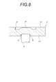
- FIG. 7 is a diagram illustrating an optical lens manufacturing process following FIG. 6. It is a figure which expands and shows the part enclosed by the dotted-line circle VIII in FIG.
- FIG. 1 shows an example of the configuration of an imaging apparatus for explaining an embodiment of the present invention.
- An imaging apparatus 1 shown in FIG. 1 includes a sensor substrate 2 on which a solid-state imaging device 3 such as a CCD (Charge-Coupled Device) image sensor or a CMOS (Complementary Metal-Oxide-Semiconductor) image sensor is mounted, and an image receiving surface of the solid-state imaging device 3. And a lens unit 4 for forming an image.
- the imaging device 1 is used as a camera mounted on a mobile terminal such as a smartphone or a mobile phone.
- the lens unit 4 includes a plurality of optical lenses 10 and a lens barrel 11 that houses these optical lenses 10.
- a plurality of optical lenses 10 are laminated with their optical axes aligned, and are housed in a lens barrel 11.
- a fitting portion 12 corresponding to each optical lens 10 is provided on the inner periphery of the lens barrel 11. The optical axes of the plurality of optical lenses 10 are aligned by fitting each optical lens 10 to the corresponding fitting portion 12.
- Each optical lens 10 has an optical function part 20 having a refractive power and a flange part 21 provided around the optical function part 20.
- the first surface 20a and the second surface 20b of the optical function unit 20 that face each other in the optical axis direction are formed on a curved surface or a flat surface such as a convex spherical surface, a concave spherical surface, or an aspherical surface, for example, and an appropriate combination of these surface shapes.
- the optical function unit 20 is given a desired refractive power.
- Each optical lens 10 is laminated with its flange portion 21 in contact with the flange portion 21 of the adjacent optical lens 10.
- both optical lenses 10 may be stacked with a spacer interposed between the flange portions 21 of two adjacent optical lenses 10.
- the optical axes of the plurality of optical lenses 10 are aligned by fitting each optical lens 10 with the corresponding fitting portion 12 of the lens barrel 11.
- the optical axis of the plurality of optical lenses 10 may be aligned by fitting the flange portion 21 with a flange portion 21 or a spacer of another optical lens 10 in contact with the flange portion 21.
- the optical lens 10 is a plastic lens formed by molding and solidifying an optical resin material using a mold.
- One of the first surface 21a and the second surface 21b of the flange portion 21 facing in the optical axis direction is pressed by an ejector pin of the molding die described later when released from the molding die.
- a pressed portion 22 is provided.
- the pressed portions 22 are recessed at a plurality of locations on the first surface 21a of the flange portion 21 with an interval in the circumferential direction.
- a region of the first surface 21 a excluding the pressed portion 22 is a contact portion with another optical lens 10 provided adjacently in the lens unit 4.
- a plurality of recesses 23 are provided on the second surface 21b of the flange portion 21 opposite to the first surface 21a. These recesses 23 are provided in regions facing each of the pressed parts 22 in the optical axis direction of the optical lens 10.
- the recessed part 23 is formed in the substantially fan shape in the example of illustration, the shape is not specifically limited, For example, a substantially circular shape may be sufficient and a substantially rectangular shape may be sufficient.
- a region of the second surface 21 b excluding the concave portion 23 is a contact portion with another optical lens 10 provided adjacently in the lens unit 4.
- Examples of the optical resin material that forms the optical lens 10 include thermoplastic resins such as cycloolefin polymer (COP), cycloolefin copolymer (COC), polymethyl methacrylate (PMMA), and polycarbonate (PC), and epoxy (EP). Examples of the thermosetting resin or photo-curing resin can be given.
- thermoplastic resins such as cycloolefin polymer (COP), cycloolefin copolymer (COC), polymethyl methacrylate (PMMA), and polycarbonate (PC), and epoxy (EP).
- COP cycloolefin polymer
- COC cycloolefin copolymer
- PMMA polymethyl methacrylate
- PC polycarbonate
- EP epoxy
- thermosetting resin or photo-curing resin can be given.
- FIG. 4 shows the configuration of the mold of the optical lens 10.
- the mold 30 is for molding the optical resin material into the optical lens 10 by injection molding, and includes a first mold plate 31, a second mold plate 32, and a plurality of ejector pins 33.
- the first template 31 and the second template 32 are arranged to face each other, and the second template 32 is advanced and retracted in the opposing direction with respect to the first template 31.
- the opposing surfaces of the first mold plate 31 and the second mold plate 32 are integrally formed with cavities, and molding surfaces 34 and 35 for molding the optical resin material filled in the cavities into the optical lens 10 are formed. Is provided.
- the molding surface 34 of the first template 31 includes an optical function portion molding surface 36 formed in a shape obtained by inverting the shape of the first surface 20 a of the optical function portion 20 of the optical lens 10, and the first surface 21 a of the flange portion 21.
- the flange portion forming surface 37 is formed to have a shape obtained by reversing the shape.
- the molding surface 35 of the second template 32 includes an optical function part molding surface 38 formed in a shape obtained by inverting the shape of the second surface 20 b of the optical function part 20 of the optical lens 10, and the second surface 21 b of the flange part 21.
- the flange portion forming surface 39 is formed to have a shape obtained by reversing the shape.
- a plurality of convex portions 40 are provided on the flange portion molding surface 37 of the first template 31 at intervals in the circumferential direction.
- Each convex portion 40 shapes the pressed portion 22 that is recessed in the first surface 21 a of the flange portion 21 of the optical lens 10.
- the first template 31 is provided with a plurality of receiving holes 41 for receiving the ejector pins 33, respectively.
- Each accommodation hole 41 extends in the opposing direction of the first mold plate 31 and the second mold plate 32, and is formed to open at the end surface of the convex portion 40 provided on the flange portion molding surface 37.
- Each ejector pin 33 is accommodated in an accommodation hole 41 formed in the first mold 31, and is driven forward and backward in the opposing direction of the first mold 31 and the second mold 32 to open the accommodation hole 41.
- the protrusion 40 is provided so as to protrude from the end surface.
- a plurality of convex portions 42 are provided on the flange portion molding surface 39 of the second template 32. These convex portions 42 are provided in regions facing each of the ejector pins 33 exposed at the opening of the accommodation hole 41 of the first template 31. Each convex portion 42 forms a concave portion 23 that is recessed in the second surface 21 b of the flange portion 21 of the optical lens 10.
- FIG. 5 to 7 show the manufacturing process of the optical lens 10 using the mold 30.
- the first mold plate 31 and the second mold plate 32 are in close contact with each other, and the mold 30 is closed.
- An optical resin material is injected into the cavity.
- the optical resin material filled in the cavity is deformed along the molding surfaces 34 and 35 to be molded into the optical lens 10 and solidified in the cavity.
- the optical resin material is a thermoplastic resin, it is solidified by being cooled through the mold plates 31 and 32, and if it is a photo-curable resin, it is solidified by being irradiated with light through the mold plates 31 and 32. If it is curable resin, it will be solidified by heating through the template 31 and 32.
- the second mold plate 32 is retracted, and the mold 30 is opened.
- the optical lens 10 formed by solidifying the optical resin material is fixed to the molding surface 34 of the first template 31 and remains on the first template 31.
- the ejector pin 33 is driven.
- the ejector pin 33 protrudes from the end surface of the convex portion 40 where the accommodation hole 41 is opened, and the convex portion 40 presses the pressed portion 22 formed on the first surface 21 a of the flange portion 21 of the optical lens 10. Thereby, the optical lens 10 is released from the first template 31.
- FIG. 8 shows the configuration of the flange portion 21 of the optical lens 10 in detail.
- the raised portion is raised in the pressing direction as the pressed portion 22 is pressed by the ejector pin 33.
- Part 25 is produced.
- a recessed portion 23 is provided in a region facing the pressed portion 22 on the second surface 21 b of the flange portion 21, and the raised portion 25 does not protrude from the second surface 21 b of the flange portion 21.
- the amount of protrusion from the second surface 21b is reduced. For this reason, the wave
- a burr 24 is generated in the pressed portion 22 provided on the first surface 21 a of the flange portion 21.
- the burr 24 is formed by solidifying the optical resin material that has entered the accommodation hole 41 of the mold 30 that accommodates the ejector pin 33.
- the pressed portion 22 is recessed in the first surface 21 a of the flange portion 21, and the burr 24 is accommodated in the pressed portion 22 without protruding from the first surface 21 a of the flange portion 21.
- the flatness of the first surface 21a excluding the pressed portion 22 is maintained, and the accuracy of the lens interval of the plurality of optical lenses 10 stacked with the flange portions 21 in contact with each other is more reliably maintained.
- the recessed portion 23 is formed larger than the pressed portion 22 so as to cover the pressed portion 22 when viewed from the optical axis direction as in the illustrated example.
- the convex part 42 of the second mold plate 32 that forms the concave part 23 covers the ejector pin 33 that presses the pressed part 22 when viewed from the opposing direction of the first mold plate 31 and the second mold plate 32. It is formed larger than the ejector pin 33.
- the skirt of the raised portion 25 may spread around the pressed portion 22, the raised portion 25 can be more reliably accommodated in the recessed portion 23 by forming the recessed portion 23 larger than the pressed portion 22. Can do. Thereby, the flatness of the flange portion 21 can be more reliably maintained.
- the raised portion 25 tends to be higher. Further, in relation to the thickness of the flange portion 21, the protruding portion 25 tends to increase as the pressure applied to the pressed portion 22 increases by being pressed by the ejector pin 33.
- the pressure applied to the pressed portion 22 is determined by the fixing force of the optical lens 10 to the first template 31, the cross-sectional area of each ejector pin 33 that presses the pressed portion 22, and the sum thereof. Therefore, the ratio of the outer diameter of the optical lens 10 and the thickness of the flange portion 21 related to the fixing force of the optical lens 10 to the first mold plate 31 (the outer diameter of the optical lens 10 / the thickness of the flange portion 21), and each The cross-sectional area of the ejector pin 33 and the total sum thereof were variously changed, and the flatness of the flange portion 21 when the concave portion 23 was not provided was evaluated using a small-diameter laser interferometer (FI251LN manufactured by Fuji Film).
- the ejector pin 33 is formed in a columnar shape having a substantially uniform outer diameter. For this reason, the cross-sectional area of the ejector pin 33 is equivalent to the area of the surface of the ejector pin 33 that contacts the first surface 21 a of the flange portion 21.
- A indicates that no bulging is observed in the flange portion 21
- B indicates that the bulging is within the allowable range
- C indicates that the bulging is permitted and exceeds the allowable range.
- D The case where damage occurs is shown as D.
- the allowable range of the protrusion of the flange portion 21 is set to 1 ⁇ m in consideration of an error allowed in the lens interval in the lens unit of the camera mounted on the portable terminal.
- the thickness of the flange portion 21 is 0.1 mm or more. 1.0 mm or less is suitable.
- the flange portion 21 is prominently raised when the ratio of the outer diameter of the optical lens 10 to the thickness of the flange portion 21 (lens outer diameter / flange thickness) is 5.0 or more and 50.0 or less. (Experimental examples 7 to 24, 37 to 42). When the ratio of the outer diameter of the optical lens 10 and the thickness of the flange portion 21 is less than 5.0, the relative strength of the flange portion 21 with respect to the fixing force of the optical lens 10 to the first template 31 is sufficient. In this case, the flange 21 has no or slightly raised portions (Experimental Examples 1 to 6, 31 to 36).
- the ratio between the outer diameter of the optical lens 10 and the thickness of the flange portion 21 is larger than 50.0, the relative strength of the flange portion 21 with respect to the fixing force of the optical lens 10 to the first template 31 is high.
- the flange portion 21 is damaged due to excessive shortage (Experimental Examples 25 to 30). From these results, the outer diameter of the optical lens 10 and the flange portion 21 are maintained in order to maintain the flatness of the flange portion 21 by providing the concave portion 23 in the region facing the pressed portion 22 on the second surface 21b of the flange portion 21.
- the ratio with the thickness is preferably 5.0 or more and 50.0 or less.
- each ejector pin 33 0.07 mm 2 or more 0.20 mm 2 or less (0.3mm or 0.5mm or less in terms of diameter) is preferred, the cross-sectional area of the plurality of ejector pins 33 The total sum is preferably 0.2 mm 2 or more and 1.5 mm 2 or less.
- the pressed portion 22 is ejected from the ejector pin 33.
- the flatness of the flange portion 21 can be maintained also by the local bulge that is caused by being pressed by.
- the lens interval of the plurality of optical lenses 10 stacked with the flange portions 21 in contact with each other can be maintained with the designed accuracy, and the lens unit 4 in which the plurality of optical lenses 10 are stacked and The performance of the imaging device 1 including the lens unit 4 can be obtained stably.
- molding die 30 demonstrated as what shape
- the imaging device 1 is not limited to a camera mounted on a mobile terminal such as a smartphone, but as a vehicle-mounted camera or a specification equivalent to a camera mounted on a mobile terminal (for example, 8 million pixels or more, F value 2). .4 or more, and the total length of the optical system is 6 mm or less).
- An imaging apparatus comprising: the lens unit according to (6); and an imaging element that captures an optical image formed by the lens unit.
- the imaging device according to (7) which is mounted on a mobile terminal.
- (11) The molding die according to (9) or (10), wherein an interval between the flange portion molding surfaces of the first mold plate and the second mold plate is 0.1 mm or more and 1 mm or less. Type.
Landscapes
- Engineering & Computer Science (AREA)
- Manufacturing & Machinery (AREA)
- Mechanical Engineering (AREA)
- Physics & Mathematics (AREA)
- Lens Barrels (AREA)
- General Physics & Mathematics (AREA)
- Optics & Photonics (AREA)
- Moulds For Moulding Plastics Or The Like (AREA)
Abstract
光学レンズのフランジ部の平坦性を高め性能を安定に得ることができる、光学レンズ、成形型、複数枚の光学レンズが積層されたレンズユニット及びこのレンズユニットを備える撮像装置を提供する。成形型を用いて光学樹脂材料を成形、固化して形成される光学レンズは、光学機能部と、光学機能部の周囲に設けられたフランジ部と、を有し、フランジ部は、光学レンズの光軸方向に対向する第一面及び第二面を有し、第一面には、光学レンズを成形型から離型させるイジェクタピンによって押圧される複数の被押圧部が設けられており、第二面には、光学レンズの光軸方向に被押圧部の各々と対向する領域に、複数の凹部が設けられている。
Description
本発明は、光学レンズ、その成形型、この光学レンズを備えるレンズユニット及び撮像装置に関する。
スマートフォンや携帯電話などの携帯端末に搭載されるカメラ、車載カメラ、等の比較的小型の撮像装置において、その光学系は、典型的には複数枚の光学レンズが積層されたレンズユニットで構成される。そして光学レンズには、プラスチックレンズが多用されている。
プラスチックレンズは、圧縮成形や射出成形によって製造される。具体的には、プラスチックレンズは、光学樹脂材料を成形型で所望の形状に成形、固化させ、これをイジェクタピンで押圧して離型させるようにして、製造される。このようにして製造されるプラスチックレンズは、一般に、屈折力を有する光学機能部と、光学機能部の周囲に設けられたフランジ部とを有しており、フランジ部がイジェクタピンによって押圧される(例えば、特許文献1、2参照)。
そして、複数枚のプラスチックレンズが積層されたレンズユニットでは、例えば各プラスチックレンズのフランジ部を、隣設されるプラスチックレンズのフランジ部に当接させて複数枚のプラスチックレンズが積層され、これらのプラスチックレンズは鏡筒に収納されて保持される。
離型の際にイジェクタピンによって押圧されるフランジ部の被押圧部には、通常バリが生じる。フランジ部に生じるバリは、鏡筒や鏡枠などの保持体へのプラスチックレンズの組み込みに影響を及ぼす可能性がある。そこで、特許文献2に記載されたプラスチックレンズでは、被押圧部がフランジ部に凹設されており、被押圧部に生じるバリが被押圧部内に収容されるように構成されている。
携帯端末に搭載されるカメラや車載カメラの小型化に伴い、この種の撮像装置に用いられるレンズユニットには小型化が要請されている。レンズユニットの小型化に伴い、レンズユニットの光軸方向の寸法には高い精度が求められ、レンズユニットの光軸方向の寸法精度に影響するレンズ間隔にも高い精度が求められる。例えば、携帯端末に搭載されるカメラのレンズユニットは、典型的には5枚前後のプラスチックレンズが用いられているところ、レンズユニットの光軸方向の寸法に許容される誤差は±数μm程度とされており、各レンズ間隔に許容される誤差は±1μm程度となる。
また、レンズユニットの小型化に伴い、レンズユニットを構成する個々のプラスチックレンズは薄肉化される傾向にある。例えば、携帯端末に搭載されるカメラのレンズユニットでは、フランジ部の厚みが1mm以下のプラスチックレンズが用いられるようになっている。
ところが、プラスチックレンズの薄肉化に起因して、フランジ部の裏面に設けられている被押圧部がイジェクタピンによって押圧されるのに伴い、フランジ部の表面において被押圧部に重なる領域が押圧方向に局所的に隆起してフランジ部に周方向のうねりが生じ、フランジ部の平坦性が損なわれる虞がある。そして、フランジ部の平坦性が損なわれると、レンズ間隔の精度も低下し、それに起因してレンズユニットの光学性能が低下し、撮像装置によって撮像される画像の画質が低下する虞がある。
本発明は、上述した事情に鑑みなされたものであり、その目的は、光学レンズのフランジ部の平坦性を高め、複数枚の光学レンズが積層されたレンズユニット及びこのレンズユニットを備える撮像装置の性能を安定に得ることにある。
(1) 成形型を用いて光学樹脂材料を成形、固化して形成される光学レンズであって、光学機能部と、光学機能部の周囲に設けられたフランジ部と、を有し、フランジ部は、光学レンズの光軸方向に対向する第一面及び第二面を有し、第一面には、光学レンズを成形型から離型させるイジェクタピンによって押圧される複数の被押圧部が設けられており、第二面には、光軸方向に被押圧部の各々と対向する領域に、複数の凹部が設けられている光学レンズ。
(2) 複数の光学レンズが、それら複数の光学レンズの光軸を揃えて積層されたレンズユニットであって、複数の光学レンズのうち少なくとも一つの光学レンズが、(1)に記載された光学レンズであるレンズユニット。
(3) (2)に記載のレンズユニットと、レンズユニットによって形成される光像を撮像する撮像素子と、を備える撮像装置。
(4) 光学樹脂材料を、光学機能部と、光学機能部の周囲に設けられたフランジ部と、を有する光学レンズに成形する成形型であって、互いに対向して配置され、光学レンズの光軸方向に対向するフランジ部の第一面及び第二面の形状を光学樹脂材料に転写するフランジ部成形面が設けられた第一型板及び第二型板と、第一型板及び第二型板の対向方向に進退駆動されて第一型板のフランジ部成形面から突出可能に第一型板に設けられた複数のイジェクタピンと、を備え、第二型板のフランジ部成形面には、複数のイジェクタピンの各々と対向する領域に、複数の凸部が設けられている成形型。
(2) 複数の光学レンズが、それら複数の光学レンズの光軸を揃えて積層されたレンズユニットであって、複数の光学レンズのうち少なくとも一つの光学レンズが、(1)に記載された光学レンズであるレンズユニット。
(3) (2)に記載のレンズユニットと、レンズユニットによって形成される光像を撮像する撮像素子と、を備える撮像装置。
(4) 光学樹脂材料を、光学機能部と、光学機能部の周囲に設けられたフランジ部と、を有する光学レンズに成形する成形型であって、互いに対向して配置され、光学レンズの光軸方向に対向するフランジ部の第一面及び第二面の形状を光学樹脂材料に転写するフランジ部成形面が設けられた第一型板及び第二型板と、第一型板及び第二型板の対向方向に進退駆動されて第一型板のフランジ部成形面から突出可能に第一型板に設けられた複数のイジェクタピンと、を備え、第二型板のフランジ部成形面には、複数のイジェクタピンの各々と対向する領域に、複数の凸部が設けられている成形型。
本発明によれば、光学レンズのフランジ部の平坦性を高めることができ、複数枚の光学レンズが積層されたレンズユニット及びこのレンズユニットを備える撮像装置の性能を安定に得ることができる。
図1は、本発明の実施形態を説明するための、撮像装置の一例の構成を示す。
図1に示す撮像装置1は、CCD(Charge Coupled Device)イメージセンサやCMOS(Complementary Metal Oxide Semiconductor)イメージセンサなどの固体撮像素子3が実装されたセンサ基板2と、固体撮像素子3の受像面に結像するレンズユニット4とを備えている。この撮像装置1は、例えばスマートフォンや携帯電話機などの携帯端末に搭載されるカメラとして用いられる。
レンズユニット4は、複数枚の光学レンズ10と、これらの光学レンズ10を収納する鏡筒11とを備えている。複数枚の光学レンズ10は光軸を揃えて積層され、鏡筒11に収納されている。図示の例では、鏡筒11の内周に、各光学レンズ10に対応する嵌合部12が設けられている。各光学レンズ10が、対応する嵌合部12に嵌合することによって、複数枚の光学レンズ10の光軸が揃えられている。
各光学レンズ10は、屈折力を有する光学機能部20と、光学機能部20の周囲に設けられたフランジ部21とを有している。光軸方向に対向する光学機能部20の第一面20a及び第二面20bは、例えば凸球面や凹球面や非球面といった曲面又は平面に形成されており、これらの面形状の適宜な組み合わせによって、光学機能部20に所望の屈折力が付与されている。
各光学レンズ10はそのフランジ部21を、隣設される光学レンズ10のフランジ部21に当接させて積層されている。なお、隣り合う2枚の光学レンズ10のフランジ部21の間にスペーサを介在させて、両光学レンズ10が積層される場合もある。また、図示の例では、各光学レンズ10が鏡筒11の対応する嵌合部12と嵌合することによって複数枚の光学レンズ10の光軸が揃えられているが、例えば各光学レンズ10のフランジ部21を、このフランジ部21に当接する他の光学レンズ10のフランジ部21やスペーサと嵌合させることによって複数枚の光学レンズ10の光軸を揃えるようにしてもよい。
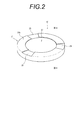
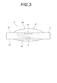
図2及び図3は、光学レンズ10の構成を示す。
光学レンズ10は、成形型を用いて光学樹脂材料を成形、固化して形成されたプラスチックレンズである。
光軸方向に対向するフランジ部21の第一面21a及び第二面21bのうち一方の第一面21aには、成形型から離型される際に、後述する成形型のイジェクタピンによって押圧される被押圧部22が設けられている。被押圧部22は、周方向に間隔をあけてフランジ部21の第一面21aの複数箇所に凹設されている。第一面21aの被押圧部22を除く領域は、レンズユニット4において隣設される他の光学レンズ10との当接部となる。
フランジ部21の第一面21aとは反対側の第二面21bには、複数の凹部23が設けられている。これらの凹部23は、光学レンズ10の光軸方向に被押圧部22の各々と対向する領域に設けられている。なお、凹部23は、図示の例では略扇形状に形成されているが、その形状は特に限定されるものではなく、例えば略円形状であってもよいし、略矩形状であってもよい。第二面21bの凹部23を除く領域は、レンズユニット4において隣設される他の光学レンズ10との当接部となる。
光学レンズ10を形成する光学樹脂材料としては、例えばシクロオレフィンポリマー(COP)、シクロオレフィンコポリマー(COC)、ポリメチルメタクリレート(PMMA)、ポリカーボネート(PC)等の熱可塑性樹脂や、エポキシ(EP)等の熱硬化性又は光硬化性樹脂などを例示することができる。
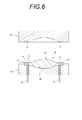
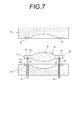
図4は、光学レンズ10の成形型の構成を示す。
成形型30は、上記の光学樹脂材料を射出成形によって光学レンズ10に成形するものであり、第一型板31及び第二型板32と、複数のイジェクタピン33とを備えている。
第一型板31及び第二型板32は互いに対向して配置されており、第二型板32が第一型板31に対して対向方向に進退される。第一型板31及び第二型板32の各々の対向面には、一体となってキャビティを形成し、このキャビティに充填される光学樹脂材料を光学レンズ10に成形する成形面34,35が設けられている。
第一型板31の成形面34は、光学レンズ10の光学機能部20の第一面20aの形状を反転した形状に形成された光学機能部成形面36、及びフランジ部21の第一面21aの形状を反転した形状に形成されたフランジ部成形面37を含んで構成されている。
第二型板32の成形面35は、光学レンズ10の光学機能部20の第二面20bの形状を反転した形状に形成された光学機能部成形面38、及びフランジ部21の第二面21bの形状を反転した形状に形成されたフランジ部成形面39を含んで構成されている。
第一型板31のフランジ部成形面37には、周方向に間隔をあけて複数の凸部40が設けられている。各凸部40は、光学レンズ10のフランジ部21の第一面21aに凹設される被押圧部22を成形する。
第一型板31には、イジェクタピン33をそれぞれ収容する複数の収容孔41が設けられている。各収容孔41は、第一型板31と第二型板32との対向方向に延在し、フランジ部成形面37に設けられた凸部40の端面に開口して形成されている。
各イジェクタピン33は、第一型板31に形成された収容孔41に収容されており、第一型板31と第二型板32との対向方向に進退駆動され、収容孔41が開口する凸部40の端面から突出可能に設けられている。
第二型板32のフランジ部成形面39には、複数の凸部42が設けられている。これらの凸部42は、第一型板31の収容孔41の開口に露呈するイジェクタピン33の各々と対向する領域に設けられている。各凸部42は、光学レンズ10のフランジ部21の第二面21bに凹設される凹部23を成形する。
図5から図7は、成形型30を用いた光学レンズ10の製造工程を示す。
まず、図5に示すように、第一型板31と第二型板32とが密接して成形型30が閉じられた状態で、両型板31,32の成形面34,35によって形成されるキャビティに光学樹脂材料が射出される。キャビティに充填された光学樹脂材料は、成形面34,35に倣って変形されて光学レンズ10に成形され、キャビティ内にて固化される。
光学樹脂材料が熱可塑性樹脂であれば型板31,32を介して冷却されることによって固化され、光硬化性樹脂であれば型板31,32を通して光照射されることによって固化され、また熱硬化性樹脂であれば型板31,32を介して加熱されることによって固化される。
続いて、図6に示すように、第二型板32が後退され、成形型30が開かれる。光学樹脂材料が固化してなる光学レンズ10は、第一型板31の成形面34に固着しており、第一型板31に残される。
続いて、図7に示すように、イジェクタピン33が駆動される。イジェクタピン33は、収容孔41が開口する凸部40の端面から突出し、この凸部40によって光学レンズ10のフランジ部21の第一面21aに成形された被押圧部22を押圧する。それにより、光学レンズ10が第一型板31から離型される。
図8は、光学レンズ10のフランジ部21の構成を詳細に示す。
フランジ部21の第二面21bにおいて、光軸方向に対して被押圧部22に対向する領域には、被押圧部22がイジェクタピン33によって押圧されることに伴って、押圧方向に隆起した隆起部25が生じている。ここで、フランジ部21の第二面21bにおいて被押圧部22に対向する領域には凹部23が設けられており、隆起部25は、フランジ部21の第二面21bから突出することなく凹部23内に収容される、又は第二面21bからの突出量を縮小される。このため、隆起部25によるフランジ部21のうねりが防止ないし抑制される。それにより、凹部23を除く第二面21bの平坦性が保たれ、フランジ部21同士を当接させて積層される複数枚の光学レンズ10のレンズ間隔が設計通りの精度に維持される。
また、フランジ部21の第一面21aに設けられた被押圧部22には、バリ24が生じている。このバリ24は、イジェクタピン33を収容している成形型30の収容孔41に浸入した光学樹脂材料が固化することによって形成される。ここで、被押圧部22はフランジ部21の第一面21aに凹設されており、バリ24は、フランジ部21の第一面21aから突出することなく被押圧部22内に収容される。それにより、被押圧部22を除く第一面21aの平坦性が保たれ、フランジ部21同士を当接させて積層される複数枚の光学レンズ10のレンズ間隔の精度がより確実に維持される。
好ましくは、凹部23は、図示の例のように、光軸方向から見たときに被押圧部22を覆うように被押圧部22より大きく形成される。凹部23を形成する第二型板32の凸部42は、第一型板31及び第二型板32の対向方向から見たときに、被押圧部22を押圧するイジェクタピン33を覆うようにイジェクタピン33より大きく形成される。隆起部25の裾野が被押圧部22の周囲にも広がる場合があるが、凹部23を被押圧部22より大きく形成しておくことによって、隆起部25をより確実に凹部23内に収容することができる。それにより、フランジ部21の平坦性をより確実に保つことができる。
フランジ部21が薄いほどに隆起部25は高くなる傾向にある。また、フランジ部21の厚みに関連して、イジェクタピン33によって押圧されることで被押圧部22にかかる圧力が大きいほどに隆起部25は高くなる傾向にある。
被押圧部22にかかる圧力は、光学レンズ10の第一型板31への固着力と、被押圧部22を押圧する各イジェクタピン33の断面積及びその総和とによって定まる。そこで、光学レンズ10の第一型板31への固着力に関連する光学レンズ10の外径とフランジ部21の厚みとの比(光学レンズ10の外径/フランジ部21の厚み)、及び各イジェクタピン33の断面積及びその総和を種々に変えて、凹部23が設けられていない場合のフランジ部21の平坦性を小口径レーザー干渉計(富士フイルム社製 FI251LN)を用いて評価した。評価結果を表1に示す。本実施形態においてイジェクタピン33は、外径が略均一な柱状に形成されている。このため、イジェクタピン33の断面積は、フランジ部21の第一面21aと接触するこのイジェクタピン33の面の面積と同等になる。
なお、表1において、フランジ部21に隆起が認められない場合をA、隆起は認められるが許容範囲内である場合をB、隆起が認められ且つ許容範囲を超える場合をC、フランジ部21に破損が生じた場合をDとして示してある。また、フランジ部21の隆起の許容範囲は、携帯端末に搭載されるカメラのレンズユニットにおいてレンズ間隔に許容される誤差を考慮して、1μmとした。

表1に示す評価結果から、フランジ部21の厚み(フランジ厚)が0.1mm以上1.0mm以下である場合にフランジ部21の隆起が顕著であることがわかる(実験例7~24,37~42)。フランジ部21の厚みが1.0mmより大きい場合には、フランジ部21の絶対的な強度が十分であり、フランジ部21に隆起は生ぜず又は僅かである(実験例1~6)。一方、フランジ部21の厚みが0.1mm未満である場合には、フランジ部21の絶対的な強度が過度に不足し、フランジ部21が破損する(実験例25~30)。これらの結果から、フランジ部21の第二面21bにおいて被押圧部22に対向する領域に凹部23を設けることによってフランジ部21の平坦性を保つうえで、フランジ部21の厚みは0.1mm以上1.0mm以下が好適である。
また、光学レンズ10の外径とフランジ部21の厚みとの比(レンズ外径/フランジ厚)が5.0以上50.0以下である場合にフランジ部21の隆起が顕著であることがわかる(実験例7~24,37~42)。光学レンズ10の外径とフランジ部21の厚みとの比が5.0未満である場合には、光学レンズ10の第一型板31への固着力に対するフランジ部21の相対的な強度が十分であり、フランジ部21に隆起は生ぜず又は僅かである(実験例1~6,31~36)。一方、光学レンズ10の外径とフランジ部21の厚みとの比が50.0より大きい場合には、光学レンズ10の第一型板31への固着力に対するフランジ部21の相対的な強度が過度に不足し、フランジ部21が破損する(実験例25~30)。これらの結果から、フランジ部21の第二面21bにおいて被押圧部22に対向する領域に凹部23を設けることによってフランジ部21の平坦性を保つうえで、光学レンズ10の外径とフランジ部21の厚みとの比は5.0以上50.0以下が好適である。
また、各イジェクタピン33の断面積は、0.07mm2以上0.20mm2以下(直径に換算して0.3mm以上0.5mm以下)が好適であり、複数のイジェクタピン33の断面積の総和は、0.2mm2以上1.5mm2以下が好適である。
以上、説明したように、光学レンズ10のフランジ部21の第二面21bにおいて光軸方向に被押圧部22に対向する領域に凹部23を設けておくことにより、被押圧部22がイジェクタピン33によって押圧されることに伴う局所的な隆起によっても、フランジ部21の平坦性を保つことができる。それにより、フランジ部21同士を当接させて積層される複数枚の光学レンズ10のレンズ間隔を設計通りの精度に維持することができ、複数枚の光学レンズ10が積層されたレンズユニット4及びこのレンズユニット4を備える撮像装置1の性能を安定に得ることができる。
なお、成形型30は、光学樹脂材料を射出成形によって光学レンズ10に成形するものとして説明したが、圧縮成形によって光学レンズ10に成形するものであってもよい。
また、撮像装置1は、スマートフォン等の携帯端末に搭載されるカメラに限らず、車載カメラとして、また、携帯端末に搭載されるカメラと同等のスペック(例えば、画素数800万以上、F値2.4以上、光学系全長6mm以下)を有するカメラとしても好適に用いることができる。
以上説明したように、本明細書には、次の事項が開示されている。
(1) 成形型を用いて光学樹脂材料を成形、固化して形成される光学レンズであって、光学機能部と、上記光学機能部の周囲に設けられたフランジ部と、を有し、上記フランジ部は、光学レンズの光軸方向に対向する第一面及び第二面を有し、上記第一面には、光学レンズを上記成形型から離型させるイジェクタピンによって押圧される複数の被押圧部が設けられており、上記第二面には、光学レンズの光軸方向に上記被押圧部の各々と対向する領域に、複数の凹部が設けられている光学レンズ。
(2) (1)に記載の光学レンズであって、上記凹部は、上記被押圧部より大きく形成され、この光学レンズの光軸方向から見たときに上記被押圧部を覆っている光学レンズ。
(3) (1)又は(2)に記載の光学レンズであって、上記フランジ部の厚みは、0.1mm以上1mm以下である光学レンズ。
(4) (1)から(3)のいずれか一つに記載の光学レンズであって、上記フランジ部の厚みに対する光学レンズの外径の比が5.0以上50.0以下である光学レンズ。
(5) (1)から(4)のいずれか一つに記載の光学レンズであって、上記第二面に、光学レンズに積層される他の光学レンズとの当接部が設けられている光学レンズ。
(6) 複数の光学レンズが、それら複数の光学レンズの光軸を揃えて積層されたレンズユニットであって、上記複数の光学レンズのうち少なくとも一つの光学レンズが、(1)から(5)のいずれか一項に記載された光学レンズであるレンズユニット。
(7) (6)に記載のレンズユニットと、上記レンズユニットによって形成される光像を撮像する撮像素子と、を備える撮像装置。
(8) (7)に記載の撮像装置であって、携帯端末に搭載される撮像装置。
(9) 光学樹脂材料を、光学機能部と、上記光学機能部の周囲に設けられたフランジ部と、を有する光学レンズに成形する成形型であって、互いに対向して配置され、光学レンズの光軸方向に対向するフランジ部の第一面及び第二面の形状を上記光学樹脂材料に転写するフランジ部成形面が設けられた第一型板及び第二型板と、上記第一型板及び上記第二型板の対向方向に進退駆動されて上記第一型板の上記フランジ部成形面から突出可能に上記第一型板に設けられた複数のイジェクタピンと、を備え、上記第二型板の上記フランジ部成形面には、複数のイジェクタピンの各々と対向する領域に、複数の凸部が設けられている成形型。
(10) (9)に記載の成形型であって、上記凸部は、上記イジェクタピンよりも大きく形成され、上記第一型板及び上記第二型板の対向方向から見たときに上記イジェクタピンを覆っている成形型。
(11) (9)又は(10)に記載の成形型であって、上記第一型板及び上記第二型板の上記フランジ部成形面間の間隔は、0.1mm以上1mm以下である成形型。
(12) (9)から(11)のいずれか一つに記載の成形型であって、上記イジェクタピンの断面積は、0.07mm2以上0.2mm2以下である成形型。
(13) (9)から(12)のいずれか一つに記載の成形型であって、上記複数のイジェクタピンの断面積の総和が、0.2mm2以上1.5mm2以下である成形型。
(14) (9)から(13)のいずれか一つに記載の成形型であって、上記第一型板及び上記第二型板の上記フランジ部成形面間の間隔に対する上記第一型板及び上記第二型板の上記フランジ部成形面の外径の比が5.0以上50.0以下である成形型。
(2) (1)に記載の光学レンズであって、上記凹部は、上記被押圧部より大きく形成され、この光学レンズの光軸方向から見たときに上記被押圧部を覆っている光学レンズ。
(3) (1)又は(2)に記載の光学レンズであって、上記フランジ部の厚みは、0.1mm以上1mm以下である光学レンズ。
(4) (1)から(3)のいずれか一つに記載の光学レンズであって、上記フランジ部の厚みに対する光学レンズの外径の比が5.0以上50.0以下である光学レンズ。
(5) (1)から(4)のいずれか一つに記載の光学レンズであって、上記第二面に、光学レンズに積層される他の光学レンズとの当接部が設けられている光学レンズ。
(6) 複数の光学レンズが、それら複数の光学レンズの光軸を揃えて積層されたレンズユニットであって、上記複数の光学レンズのうち少なくとも一つの光学レンズが、(1)から(5)のいずれか一項に記載された光学レンズであるレンズユニット。
(7) (6)に記載のレンズユニットと、上記レンズユニットによって形成される光像を撮像する撮像素子と、を備える撮像装置。
(8) (7)に記載の撮像装置であって、携帯端末に搭載される撮像装置。
(9) 光学樹脂材料を、光学機能部と、上記光学機能部の周囲に設けられたフランジ部と、を有する光学レンズに成形する成形型であって、互いに対向して配置され、光学レンズの光軸方向に対向するフランジ部の第一面及び第二面の形状を上記光学樹脂材料に転写するフランジ部成形面が設けられた第一型板及び第二型板と、上記第一型板及び上記第二型板の対向方向に進退駆動されて上記第一型板の上記フランジ部成形面から突出可能に上記第一型板に設けられた複数のイジェクタピンと、を備え、上記第二型板の上記フランジ部成形面には、複数のイジェクタピンの各々と対向する領域に、複数の凸部が設けられている成形型。
(10) (9)に記載の成形型であって、上記凸部は、上記イジェクタピンよりも大きく形成され、上記第一型板及び上記第二型板の対向方向から見たときに上記イジェクタピンを覆っている成形型。
(11) (9)又は(10)に記載の成形型であって、上記第一型板及び上記第二型板の上記フランジ部成形面間の間隔は、0.1mm以上1mm以下である成形型。
(12) (9)から(11)のいずれか一つに記載の成形型であって、上記イジェクタピンの断面積は、0.07mm2以上0.2mm2以下である成形型。
(13) (9)から(12)のいずれか一つに記載の成形型であって、上記複数のイジェクタピンの断面積の総和が、0.2mm2以上1.5mm2以下である成形型。
(14) (9)から(13)のいずれか一つに記載の成形型であって、上記第一型板及び上記第二型板の上記フランジ部成形面間の間隔に対する上記第一型板及び上記第二型板の上記フランジ部成形面の外径の比が5.0以上50.0以下である成形型。
1 撮像装置
4 レンズユニット
10 光学レンズ
20 光学機能部
21 フランジ部
22 被押圧部
23 凹部
30 成形型
31 第一型板
32 第二型板
33 イジェクタピン
34 成形面
35 成形面
37 フランジ部成形面
39 フランジ部成形面
42 凸部
4 レンズユニット
10 光学レンズ
20 光学機能部
21 フランジ部
22 被押圧部
23 凹部
30 成形型
31 第一型板
32 第二型板
33 イジェクタピン
34 成形面
35 成形面
37 フランジ部成形面
39 フランジ部成形面
42 凸部
Claims (14)
- 成形型を用いて光学樹脂材料を成形、固化して形成される光学レンズであって、
光学機能部と、
前記光学機能部の周囲に設けられたフランジ部と、
を有し、
前記フランジ部は、該光学レンズの光軸方向に対向する第一面及び第二面を有し、
前記第一面には、該光学レンズを前記成形型から離型させるイジェクタピンによって押圧される複数の被押圧部が設けられており、
前記第二面には、前記光軸方向に前記被押圧部の各々と対向する領域に、複数の凹部が設けられている光学レンズ。 - 請求項1に記載の光学レンズであって、
前記凹部は、前記被押圧部より大きく形成され、該光学レンズの光軸方向から見たときに該被押圧部を覆っている光学レンズ。 - 請求項1又は2に記載の光学レンズであって、
前記フランジ部の厚みは、0.1mm以上1mm以下である光学レンズ。 - 請求項1から3のいずれか一項に記載の光学レンズであって、
前記フランジ部の厚みに対する該光学レンズの外径の比が5.0以上50.0以下である光学レンズ。 - 請求項1から4のいずれか一項に記載の光学レンズであって、
前記第二面に、該光学レンズに積層される他の光学レンズとの当接部が設けられている光学レンズ。 - 複数の光学レンズが、該複数の光学レンズの光軸を揃えて積層されたレンズユニットであって、
前記複数の光学レンズのうち少なくとも一つの光学レンズが、請求項1から5のいずれか一項に記載の光学レンズであるレンズユニット。 - 請求項6に記載のレンズユニットと、
前記レンズユニットによって形成される光像を撮像する撮像素子と、
を備える撮像装置。 - 請求項7に記載の撮像装置であって、
携帯端末に搭載される撮像装置。 - 光学樹脂材料を、光学機能部と、前記光学機能部の周囲に設けられたフランジ部と、を有する光学レンズに成形する成形型であって、
互いに対向して配置され、光学レンズの光軸方向に対向するフランジ部の第一面及び第二面の形状を前記光学樹脂材料に転写するフランジ部成形面が設けられた第一型板及び第二型板と、
前記第一型板及び前記第二型板の対向方向に進退駆動されて前記第一型板の前記フランジ部成形面から突出可能に該第一型板に設けられた複数のイジェクタピンと、
を備え、
前記第二型板の前記フランジ部成形面には、複数のイジェクタピンの各々と対向する領域に、複数の凸部が設けられている成形型。 - 請求項9に記載の成形型であって、
前記凸部は、前記イジェクタピンよりも大きく形成され、前記第一型板及び前記第二型板の対向方向から見たときに該イジェクタピンを覆っている成形型。 - 請求項9又は10に記載の成形型であって、
前記第一型板及び前記第二型板の前記フランジ部成形面間の間隔は、0.1mm以上1mm以下である成形型。 - 請求項9から11のいずれか一項に記載の成形型であって、
前記イジェクタピンの断面積は、0.07mm2以上0.2mm2以下である成形型。 - 請求項9から12のいずれか一項に記載の成形型であって、
前記複数のイジェクタピンの断面積の総和が、0.2mm2以上1.5mm2以下である成形型。 - 請求項9から13のいずれか一項に記載の成形型であって、
前記第一型板及び前記第二型板の前記フランジ部成形面間の間隔に対する前記第一型板及び前記第二型板の前記フランジ部成形面の外径の比が5.0以上50.0以下である成形型。
Priority Applications (2)
| Application Number | Priority Date | Filing Date | Title |
|---|---|---|---|
| CN201480004703.XA CN104919341B (zh) | 2013-03-26 | 2014-03-04 | 光学透镜、成型模具、透镜单元以及摄影装置 |
| JP2015508219A JP5883989B2 (ja) | 2013-03-26 | 2014-03-04 | 成形型 |
Applications Claiming Priority (2)
| Application Number | Priority Date | Filing Date | Title |
|---|---|---|---|
| JP2013-064111 | 2013-03-26 | ||
| JP2013064111 | 2013-03-26 |
Publications (1)
| Publication Number | Publication Date |
|---|---|
| WO2014156503A1 true WO2014156503A1 (ja) | 2014-10-02 |
Family
ID=51623493
Family Applications (1)
| Application Number | Title | Priority Date | Filing Date |
|---|---|---|---|
| PCT/JP2014/055387 Ceased WO2014156503A1 (ja) | 2013-03-26 | 2014-03-04 | 光学レンズ、成形型、レンズユニット、及び撮像装置 |
Country Status (4)
| Country | Link |
|---|---|
| JP (1) | JP5883989B2 (ja) |
| CN (1) | CN104919341B (ja) |
| TW (1) | TWM481813U (ja) |
| WO (1) | WO2014156503A1 (ja) |
Cited By (3)
| Publication number | Priority date | Publication date | Assignee | Title |
|---|---|---|---|---|
| JP2017185759A (ja) * | 2016-04-08 | 2017-10-12 | キヤノン株式会社 | プラスチックレンズおよびその製造方法 |
| CN110869831A (zh) * | 2017-06-29 | 2020-03-06 | 日本电产三协株式会社 | 塑料透镜的制造方法 |
| JP2021015255A (ja) * | 2019-07-16 | 2021-02-12 | 旭化成株式会社 | 監視カメラ用レンズ及びレンズカバー |
Families Citing this family (3)
| Publication number | Priority date | Publication date | Assignee | Title |
|---|---|---|---|---|
| TWI608931B (zh) * | 2015-11-03 | 2017-12-21 | Optical lens manufacturing method, manufacturing die and product thereof | |
| JP2019012110A (ja) * | 2017-06-29 | 2019-01-24 | 日本電産サンキョー株式会社 | レンズユニット |
| CN109532068B (zh) * | 2018-11-28 | 2021-04-20 | 张家港康得新光电材料有限公司 | 压印刀具、透镜模具和视景分离元件及其制备方法 |
Citations (4)
| Publication number | Priority date | Publication date | Assignee | Title |
|---|---|---|---|---|
| JP2007245685A (ja) * | 2006-03-20 | 2007-09-27 | Matsushita Electric Ind Co Ltd | 光学素子成形金型および光学素子 |
| JP2009241531A (ja) * | 2008-03-31 | 2009-10-22 | Fujifilm Corp | 加圧成形装置及び加圧成形方法ならびに成形品 |
| WO2011078023A1 (ja) * | 2009-12-25 | 2011-06-30 | コニカミノルタオプト株式会社 | 撮像レンズユニット |
| JP2012056321A (ja) * | 2005-12-26 | 2012-03-22 | Konica Minolta Opto Inc | 樹脂成形用金型及び光ピックアップ装置用対物レンズ並びに光学素子製造方法 |
Family Cites Families (9)
| Publication number | Priority date | Publication date | Assignee | Title |
|---|---|---|---|---|
| JP4407148B2 (ja) * | 2003-04-18 | 2010-02-03 | コニカミノルタオプト株式会社 | 光学素子の製造方法及び装置並びに光学素子 |
| FR2893423B1 (fr) * | 2005-11-15 | 2007-12-21 | Bnl Eurolens Soc Par Actions S | Ebauche d'oculaire avec insert et son procede de fabrication |
| WO2008053692A1 (en) * | 2006-11-01 | 2008-05-08 | Konica Minolta Opto, Inc. | Optical element, resin molding metal die and optical element manufacturing method |
| JP5007556B2 (ja) * | 2006-11-24 | 2012-08-22 | コニカミノルタアドバンストレイヤー株式会社 | 光学素子製造方法 |
| JP2008155577A (ja) * | 2006-12-26 | 2008-07-10 | Fujifilm Corp | レンズ成形用金型およびレンズの製造方法 |
| JP2008213397A (ja) * | 2007-03-07 | 2008-09-18 | Konica Minolta Opto Inc | 樹脂成形用金型及び光学素子並びに光ピックアップ装置 |
| CN101909842A (zh) * | 2007-12-28 | 2010-12-08 | 柯尼卡美能达精密光学株式会社 | 光学元件的制造方法及光学元件成形模具 |
| JP4525868B2 (ja) * | 2008-09-29 | 2010-08-18 | コニカミノルタオプト株式会社 | 光ピックアップ用対物レンズの製造方法及び光ピックアップ用対物レンズの成形金型、並びに、光ピックアップ用対物レンズ |
| JP2013134797A (ja) * | 2011-12-27 | 2013-07-08 | Konica Minolta Advanced Layers Inc | 光ピックアップ装置用の対物レンズ |
-
2014
- 2014-03-04 JP JP2015508219A patent/JP5883989B2/ja not_active Expired - Fee Related
- 2014-03-04 CN CN201480004703.XA patent/CN104919341B/zh not_active Expired - Fee Related
- 2014-03-04 WO PCT/JP2014/055387 patent/WO2014156503A1/ja not_active Ceased
- 2014-03-26 TW TW103205133U patent/TWM481813U/zh not_active IP Right Cessation
Patent Citations (4)
| Publication number | Priority date | Publication date | Assignee | Title |
|---|---|---|---|---|
| JP2012056321A (ja) * | 2005-12-26 | 2012-03-22 | Konica Minolta Opto Inc | 樹脂成形用金型及び光ピックアップ装置用対物レンズ並びに光学素子製造方法 |
| JP2007245685A (ja) * | 2006-03-20 | 2007-09-27 | Matsushita Electric Ind Co Ltd | 光学素子成形金型および光学素子 |
| JP2009241531A (ja) * | 2008-03-31 | 2009-10-22 | Fujifilm Corp | 加圧成形装置及び加圧成形方法ならびに成形品 |
| WO2011078023A1 (ja) * | 2009-12-25 | 2011-06-30 | コニカミノルタオプト株式会社 | 撮像レンズユニット |
Cited By (5)
| Publication number | Priority date | Publication date | Assignee | Title |
|---|---|---|---|---|
| JP2017185759A (ja) * | 2016-04-08 | 2017-10-12 | キヤノン株式会社 | プラスチックレンズおよびその製造方法 |
| CN110869831A (zh) * | 2017-06-29 | 2020-03-06 | 日本电产三协株式会社 | 塑料透镜的制造方法 |
| CN110869831B (zh) * | 2017-06-29 | 2022-01-04 | 日本电产三协株式会社 | 塑料透镜的制造方法 |
| JP2021015255A (ja) * | 2019-07-16 | 2021-02-12 | 旭化成株式会社 | 監視カメラ用レンズ及びレンズカバー |
| JP7267862B2 (ja) | 2019-07-16 | 2023-05-02 | 旭化成株式会社 | 監視カメラ用レンズ及びレンズカバー |
Also Published As
| Publication number | Publication date |
|---|---|
| JP5883989B2 (ja) | 2016-03-15 |
| CN104919341A (zh) | 2015-09-16 |
| TWM481813U (zh) | 2014-07-11 |
| JPWO2014156503A1 (ja) | 2017-02-16 |
| CN104919341B (zh) | 2016-08-17 |
Similar Documents
| Publication | Publication Date | Title |
|---|---|---|
| JP5883989B2 (ja) | 成形型 | |
| JP6578279B2 (ja) | 撮像装置、光学機器、電子機器、車両および撮像装置の製造方法 | |
| CN102401911B (zh) | 晶片透镜及其制造方法 | |
| US9507116B2 (en) | Lens module | |
| US20050001145A1 (en) | Solid-state imaging device and method for manufacturing the same | |
| CN104093548B (zh) | 光学元件的制造方法 | |
| US20060284327A1 (en) | Optical unit manufacturing method, optical unit, and forming apparatus | |
| CN104115038A (zh) | 复合成形透镜及其制造方法、模具以及摄像模块 | |
| KR20120107426A (ko) | 플라스틱 렌즈, 촬영 렌즈, 촬상 장치 및 휴대 기기 | |
| KR20130003455A (ko) | 촬상 렌즈 | |
| JP2005309000A (ja) | 光学ユニット | |
| CN101441283A (zh) | 塑胶镜片及其制造方法 | |
| WO2015019768A1 (ja) | レンズアレイ、レンズアレイ積層体、及び、これらの製造方法 | |
| US20140085737A1 (en) | Lens module and manufacturing method thereof | |
| CN103116196B (zh) | 阵列光学元件制造方法 | |
| KR101113523B1 (ko) | 렌즈 사출 금형 | |
| US7369330B2 (en) | Image-forming lens set | |
| KR200451065Y1 (ko) | 사각형 광학유리 렌즈 | |
| TWI581031B (zh) | 晶圓級透鏡系統及其製造方法 | |
| JP2014085361A (ja) | レンズユニット及び撮像装置 | |
| US9429687B2 (en) | Image-capturing assembly and array lens units thereof | |
| EP1804097B1 (en) | Method of forming a ring shaped stopper for use in a camera | |
| KR102006896B1 (ko) | 카메라용 광학 렌즈 | |
| TWI604242B (zh) | 鏡頭座、其製作方法及可攜式電子裝置 | |
| TWI475678B (zh) | Array optical element manufacturing method |
Legal Events
| Date | Code | Title | Description |
|---|---|---|---|
| 121 | Ep: the epo has been informed by wipo that ep was designated in this application |
Ref document number: 14773434 Country of ref document: EP Kind code of ref document: A1 |
|
| ENP | Entry into the national phase |
Ref document number: 2015508219 Country of ref document: JP Kind code of ref document: A |
|
| NENP | Non-entry into the national phase |
Ref country code: DE |
|
| 122 | Ep: pct application non-entry in european phase |
Ref document number: 14773434 Country of ref document: EP Kind code of ref document: A1 |