WO2014148486A1 - タッチパネルおよび保護層形成用樹脂組成物 - Google Patents
タッチパネルおよび保護層形成用樹脂組成物 Download PDFInfo
- Publication number
- WO2014148486A1 WO2014148486A1 PCT/JP2014/057326 JP2014057326W WO2014148486A1 WO 2014148486 A1 WO2014148486 A1 WO 2014148486A1 JP 2014057326 W JP2014057326 W JP 2014057326W WO 2014148486 A1 WO2014148486 A1 WO 2014148486A1
- Authority
- WO
- WIPO (PCT)
- Prior art keywords
- substrate
- touch panel
- lead
- protective layer
- detection electrode
- Prior art date
- Legal status (The legal status is an assumption and is not a legal conclusion. Google has not performed a legal analysis and makes no representation as to the accuracy of the status listed.)
- Ceased
Links
Images






Classifications
-
- G—PHYSICS
- G06—COMPUTING OR CALCULATING; COUNTING
- G06F—ELECTRIC DIGITAL DATA PROCESSING
- G06F3/00—Input arrangements for transferring data to be processed into a form capable of being handled by the computer; Output arrangements for transferring data from processing unit to output unit, e.g. interface arrangements
- G06F3/01—Input arrangements or combined input and output arrangements for interaction between user and computer
- G06F3/03—Arrangements for converting the position or the displacement of a member into a coded form
- G06F3/041—Digitisers, e.g. for touch screens or touch pads, characterised by the transducing means
- G06F3/044—Digitisers, e.g. for touch screens or touch pads, characterised by the transducing means by capacitive means
- G06F3/0445—Digitisers, e.g. for touch screens or touch pads, characterised by the transducing means by capacitive means using two or more layers of sensing electrodes, e.g. using two layers of electrodes separated by a dielectric layer
-
- G—PHYSICS
- G06—COMPUTING OR CALCULATING; COUNTING
- G06F—ELECTRIC DIGITAL DATA PROCESSING
- G06F3/00—Input arrangements for transferring data to be processed into a form capable of being handled by the computer; Output arrangements for transferring data from processing unit to output unit, e.g. interface arrangements
- G06F3/01—Input arrangements or combined input and output arrangements for interaction between user and computer
- G06F3/03—Arrangements for converting the position or the displacement of a member into a coded form
- G06F3/041—Digitisers, e.g. for touch screens or touch pads, characterised by the transducing means
- G06F3/044—Digitisers, e.g. for touch screens or touch pads, characterised by the transducing means by capacitive means
- G06F3/0446—Digitisers, e.g. for touch screens or touch pads, characterised by the transducing means by capacitive means using a grid-like structure of electrodes in at least two directions, e.g. using row and column electrodes
-
- G—PHYSICS
- G06—COMPUTING OR CALCULATING; COUNTING
- G06F—ELECTRIC DIGITAL DATA PROCESSING
- G06F3/00—Input arrangements for transferring data to be processed into a form capable of being handled by the computer; Output arrangements for transferring data from processing unit to output unit, e.g. interface arrangements
- G06F3/01—Input arrangements or combined input and output arrangements for interaction between user and computer
- G06F3/03—Arrangements for converting the position or the displacement of a member into a coded form
- G06F3/041—Digitisers, e.g. for touch screens or touch pads, characterised by the transducing means
- G06F3/047—Digitisers, e.g. for touch screens or touch pads, characterised by the transducing means using sets of wires, e.g. crossed wires
-
- G—PHYSICS
- G06—COMPUTING OR CALCULATING; COUNTING
- G06F—ELECTRIC DIGITAL DATA PROCESSING
- G06F2203/00—Indexing scheme relating to G06F3/00 - G06F3/048
- G06F2203/041—Indexing scheme relating to G06F3/041 - G06F3/045
- G06F2203/04103—Manufacturing, i.e. details related to manufacturing processes specially suited for touch sensitive devices
-
- G—PHYSICS
- G06—COMPUTING OR CALCULATING; COUNTING
- G06F—ELECTRIC DIGITAL DATA PROCESSING
- G06F2203/00—Indexing scheme relating to G06F3/00 - G06F3/048
- G06F2203/041—Indexing scheme relating to G06F3/041 - G06F3/045
- G06F2203/04104—Multi-touch detection in digitiser, i.e. details about the simultaneous detection of a plurality of touching locations, e.g. multiple fingers or pen and finger
Definitions
- the present invention relates to a touch panel, and more particularly to a touch panel provided with a protective layer disposed on a lead wire containing metallic silver and gelatin.
- the present invention also relates to a resin composition for forming a protective layer used to form a protective layer covering the lead-out wiring.
- the basic structure of the touch panel includes a substrate, a detection electrode provided on the substrate for detecting an input position, and a lead wire for applying a voltage to the detection electrode.
- a method of manufacturing a detection electrode and a lead wire a method of forming a conductive thin wire of low resistance from a silver image obtained by development of a silver halide photographic light-sensitive material has been studied (Patent Document 1).
- the conductive thin line containing silver produced from the above silver halide photographic light-sensitive material has a problem that ion migration tends to occur.
- ion migration occurs between the conductive thin wires, the conductive thin wires become conductive and the circuit function is not performed.
- the wiring interval has been narrowed, and conduction of circuits by ion migration is more likely to occur.
- the bus bars and the lead-out wires be formed so as to be within a narrow frame range slightly from the edge of the panel, and the space between the wires in the peripheral wiring portion is reduced to cause conduction due to ion migration. It is easy to do.
- the inventors of the present invention formed lead wires using a silver halide photographic light-sensitive material containing gelatin and silver halide described in Patent Document 1 and examined the ion migration resistance between the lead wires. In the case where the above-described wiring interval is narrowed, the level required recently has not been reached, and further improvement has been necessary.
- An object of this invention is to provide the touch panel by which generation
- a touch panel having an input area and an outer area located outside the input area, A substrate, A detection electrode disposed on a substrate corresponding to the input area; A lead wire disposed on the substrate corresponding to the outer region and electrically connected to the detection electrode; And at least a protective layer disposed on the substrate corresponding to the outer region so as to cover the lead wire,
- the protective layer is formed using an epoxy resin, Touch panel where the lead wire contains metallic silver and gelatin.
- the protective layer contains a filler.
- a resin for forming a protective layer which contains an epoxy resin, a curing agent, and a filler, and is used to form a protective layer disposed to cover the lead-out wire electrically connected to the detection electrode of the touch panel Composition.
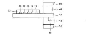
- FIG. 2 is a cross-sectional view taken along a cutting line AA shown in FIG. 1;
- FIG. 2 is a cross-sectional view taken along line BB shown in FIG. 1;
- It is an enlarged plan view of a 1st sensing electrode.
- It is a partial cross section of 2nd Embodiment of the touch panel of this invention.
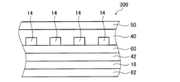
- It is a partial cross section of 3rd Embodiment of the touch panel of this invention.
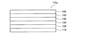
- It is a sectional view of one embodiment of an input device containing a touch panel of the present invention. It is sectional drawing of other embodiment of the input device containing the touch panel of this invention. It is sectional drawing of other embodiment of the input device containing the touch panel of this invention.
- FIG. 1 shows a plan view of a first embodiment of the touch panel 10 of the present invention.
- FIG. 2 is a cross-sectional view taken along the cutting line AA.
- FIG. 3 is a cross-sectional view taken along the cutting line BB.
- FIGS. 1 to 3 are schematic views for facilitating the understanding of the layer configuration of the touch panel, and are not drawings that accurately represent the arrangement of the layers.
- the touch panel according to this embodiment is a capacitive touch panel, and an input area E I where input operation can be performed by the user and an outer area located outside the input area E I and a E O. As shown in FIGS.
- the touch panel 10 includes a substrate 12, a first detection electrode 14 disposed on one main surface (on the surface) of the substrate 12, a first lead wire 16, and a first transparent.
- a second protective substrate 52 and a protective layer 22 are provided.
- the protective layer 22 is disposed on the substrate 12 so as to cover the first lead wiring 16 and the second lead wiring 20.
- Substrate 12 as well as responsible for supporting the first sensing electrode 14 and the second detection electrode 18 to be described later in the input region E I, the first lead wire 16 and the second lead wire 20 which will be described later in the outer region E O support Play a role in
- the substrate 12 preferably transmits light appropriately.
- the total light transmittance of the substrate 12 is preferably 85 to 100%.
- the substrate 12 preferably has an insulating property. That is, the substrate 12 is a layer for securing the insulation between the first detection electrode 14 and the second detection electrode 18.
- the substrate 12 is preferably a transparent substrate.
- an insulating resin substrate As the specific example, an insulating resin substrate, a ceramic substrate, a glass substrate etc. are mentioned, for example. Among them, an insulating resin substrate is preferable because of excellent toughness. More specifically, as a material constituting the insulating resin substrate, polyethylene terephthalate, polyether sulfone, polyacrylic resin, polyurethane resin, polyester, polycarbonate, polysulfone, polyamide, polyarylate, polyolefin, cellulose resin, poly Examples include vinyl chloride and cycloolefin resins. Among them, polyethylene terephthalate, cycloolefin resin, polycarbonate, and triacetyl cellulose resin are preferable because of excellent transparency.
- the substrate 12 is a single layer, but may be a multilayer of two or more layers.
- the thickness of the substrate 12 (the total thickness of two or more layers of the substrate 12) is not particularly limited, but is preferably 5 to 350 ⁇ m, and more preferably 30 to 150 ⁇ m. If it is in the said range, the desired transmittance
- substrate 12 is made into substantially rectangular shape, it is not restricted to this. For example, it may be circular or polygonal.
- the first detection electrode 14 and the second detection electrode 18 are sensing electrodes for sensing a change in capacitance on the touch panel 10, and constitute a sensing unit (sensor unit). That is, when the fingertip is brought into contact with the touch panel, mutual capacitance between the first detection electrode 14 and the second detection electrode 18 changes, and the position of the fingertip is calculated by the IC circuit based on the amount of change.
- the first detection electrode 14 has a role of detecting an input position in the X direction of the finger of the user approaching the input area E I , and has a function of generating a capacitance with the finger. ing.
- the first detection electrode 14 is an electrode which extends in a first direction (X direction) and is arranged at a predetermined interval in a second direction (Y direction) orthogonal to the first direction, as described later. Including patterns.
- the second detection electrode 18 has a role of detecting an input position in the Y direction of the finger of the user approaching the input area E I , and has a function of generating a capacitance with the finger. ing.
- the second detection electrode 18 is an electrode which extends in the second direction (Y direction) and is arranged at predetermined intervals in the first direction (X direction), and includes a predetermined pattern as described later. Although five first detection electrodes 14 and five second detection electrodes 18 are provided in FIG. 1, the number thereof is not particularly limited and it may be plural.
- the first detection electrode 14 and the second detection electrode 18 are formed of conductive thin lines.
- FIG. 4 shows an enlarged plan view of a part of the first detection electrode 14.
- the first detection electrode 14 is constituted by the conductive thin wires 30 and includes a plurality of lattices 32 of the conductive thin wires 30 crossing each other.
- the second detection electrode 18 also includes a plurality of grids 32 of intersecting conductive thin wires 30.
- Examples of the material of the conductive thin wire 30 include metals and alloys such as gold (Au), silver (Ag), copper (Cu) and aluminum (Al), ITO, tin oxide, zinc oxide, cadmium oxide, gallium oxide, Examples thereof include metal oxides such as titanium oxide. Among them, silver is preferable because the conductivity of the conductive thin wire 30 is excellent.
- the conductive thin wire 30 preferably contains a binder.
- the binder is preferably a water-soluble polymer because the adhesion between the conductive thin wire 30 and the substrate 12 is more excellent.
- Types of binders include, for example, gelatin, carrageenan, polyvinyl alcohol (PVA), polyvinyl pyrrolidone (PVP), polysaccharides such as starch, cellulose and derivatives thereof, polyethylene oxide, polysaccharides, polyvinyl amine, chitosan, polylysine, polyacryl Examples thereof include acids, polyalginic acids, polyhyaluronic acids, carboxycelluloses, gum arabic, sodium alginate and the like.
- gelatin is preferable because the adhesion between the conductive thin wire 30 and the substrate 12 is more excellent.
- acid-processed gelatin may be used as gelatin, and hydrolysates of gelatin, enzymatic degradation products of gelatin, gelatin modified with amino group and carboxyl group (phthalated gelatin, acetylated gelatin) Can be used.
- the volume ratio of the metal to the binder (volume of metal / volume of binder) in the conductive thin wire 30 is preferably 1.0 or more, and more preferably 1.5 or more.
- the upper limit is not particularly limited, but from the viewpoint of productivity, 4.0 or less is preferable, and 2.5 or less is more preferable.
- the volume ratio of the metal to the binder can be calculated from the density of the metal and the binder contained in the conductive thin wire 30. For example, when the metal is silver, the density of silver is 10.5 g / cm 3 , and when the binder is gelatin, the density of gelatin is 1.34 g / cm 3 .
- the line width of the conductive thin wire 30 is not particularly limited, but is preferably 30 ⁇ m or less, more preferably 15 ⁇ m or less, still more preferably 10 ⁇ m or less, and particularly preferably 9 ⁇ m or less, from the viewpoint of forming a low resistance electrode relatively easily. 7 micrometers or less are the most preferable, 0.5 micrometers or more are preferable, and 1.0 micrometers or more are more preferable.
- the thickness of the conductive fine wire 30 is not particularly limited, but can be selected from 0.00001 mm to 0.2 mm from the viewpoint of conductivity and visibility, but is preferably 30 ⁇ m or less, more preferably 20 ⁇ m or less, and 0.01 -9 ⁇ m is more preferable, and 0.05-5 ⁇ m is the most preferable.
- the grid 32 includes an open area surrounded by the conductive thin wires 30.
- the length W of one side of the grating 32 is preferably 800 ⁇ m or less, more preferably 600 ⁇ m or less, and preferably 50 ⁇ m or more.
- the first detection electrode 14 and the second detection electrode 18 preferably have an aperture ratio of 85% or more, more preferably 90% or more, and most preferably 95% or more from the viewpoint of visible light transmittance. preferable.
- the aperture ratio corresponds to the ratio of the transmissive portion excluding the conductive thin wire 30 in the first detection electrode 14 or the second detection electrode 18 in the predetermined region to the whole.
- the grid 32 has a substantially rhombus shape. However, in addition to this, it may have a polygonal shape (for example, a triangle, a square, a hexagon, or a random polygon). Moreover, the shape of one side may be a curved shape other than a linear shape, or may be an arc shape. In the case of the arc shape, for example, the two opposing sides may have an outwardly convex arc shape, and the other two opposing sides may have an inward convex arc shape. Further, the shape of each side may be a wavy line shape in which an outward convex arc and an inward convex arc are continuous. Of course, the shape of each side may be a sine curve. In addition, in FIG. 4, although the electroconductive thin wire
- the 1st detection electrode 14 and the 2nd detection electrode 18 were comprised by the mesh structure of the electroconductive thin wire 30, it is not limited to this aspect,
- metal oxidation such as ITO and ZnO Metal thin film, metal oxide particles, metal paste such as silver paste and copper paste, and metal nanowire particles such as silver nanowire and copper nanowire.
- silver nanowires are preferable in terms of excellent conductivity and transparency.
- the patterning of the electrode portion can be selected according to the material of the electrode portion, and a photolithography method, a resist mask screen printing-etching method, an inkjet method, a printing method, or the like may be used.
- the first lead-out wiring 16 and the second lead-out wiring 20 are members that play the role of applying a voltage to the first detection electrode 14 and the second detection electrode 18, respectively.
- the first lead wire 16 is disposed on substrate 12 in the outer region E O, one end is electrically connected to the first sensing electrode 14 corresponding, and the other end outside conduction such as a flexible printed wiring board is disposed It is located in the area G.
- the second lead wire 20 is disposed on substrate 12 in the outer region E O, one end is electrically connected to the second detection electrode 18 corresponding, and the other end outside conduction such as a flexible printed wiring board is disposed It is located in the area G.
- five first lead wirings 16 and five second lead wirings 20 are shown in FIG. 1, the number thereof is not particularly limited, and a plurality of the first lead wirings 16 are usually arranged according to the number of detection electrodes. Ru.
- the first lead wire 16 and the second lead wire 20 contain metallic silver and gelatin.
- the type of gelatin is not particularly limited.
- acid-processed gelatin may be used, and gelatin hydrolysates, gelatin enzyme degradates, and other amino- and carboxyl-modified gelatins (phthalates Gelatin, acetylated gelatin) can also be used.
- the first lead wire 16 and the second lead wire 20 may contain components other than metallic silver and gelatin.
- the first lead-out wiring 16 and the second lead-out wiring 20 may contain a polymer different from gelatin.
- the mass ratio of the metal silver to the polymer different from gelatin (the polymer different from metal silver / gelatin) in the first lead wire 16 and the second lead wire 20 is particularly limited. I will not.
- a protein-free polymer As a polymer different from gelatin (hereinafter, also simply referred to as a polymer), a protein-free polymer is preferable. In other words, a polymer that is not degraded by proteolytic enzymes is preferred. More specifically, for example, acrylic resin, styrene resin, vinyl resin, polyolefin resin, polyester resin, polyurethane resin, polyamide resin, polycarbonate resin, polydiene resin, epoxy resin, silicone resin Examples of the resin include at least one resin selected from the group consisting of a resin, a cellulose-based polymer and a chitosan-based polymer, and a copolymer composed of monomers constituting these resins.
- polymers which are not decomposed by a proteolytic enzyme described later are preferable, and acrylic resins, styrene resins, polyester resins and the like can be mentioned. Further, the polymer preferably has a reactive group for reacting with a crosslinking agent described later.
- a polymer (copolymer) represented by the following general formula (1) can be mentioned from the viewpoint of being capable of further preventing the penetration of water.
- A, B, C, and D each represent the following repeating unit.
- R 1 represents a methyl group or a halogen atom, preferably a methyl group, a chlorine atom or a bromine atom.
- p represents an integer of 0 to 2, preferably 0 or 1, and more preferably 0.
- R 2 represents a methyl group or an ethyl group, preferably a methyl group.
- R 3 represents a hydrogen atom or a methyl group, preferably a hydrogen atom.
- L represents a divalent linking group, preferably a group represented by the following general formula (2).
- X 1 represents an oxygen atom or -NR 30- .
- R 30 represents a hydrogen atom, an alkyl group, an aryl group or an acyl group, and each may have a substituent (eg, a halogen atom, a nitro group, a hydroxyl group or the like).
- R 30 is preferably a hydrogen atom, an alkyl group having 1 to 10 carbon atoms (eg, methyl group, ethyl group, n-butyl group, n-octyl group etc.), an acyl group (eg acetyl group, benzoyl group etc.) It is. Particularly preferred as X 1 is an oxygen atom or -NH-.
- X 2 represents an alkylene group, an arylene group, an alkylene arylene group, an arylene alkylene group, or an alkylene arylene alkylene group, and these groups include -O-, -S-, -OCO-, -CO-, -COO- , -NH-, -SO 2- , -N (R 31 )-, -N (R 31 ) SO 2 -or the like may be inserted along the way.
- R 31 represents a linear or branched alkyl group having 1 to 6 carbon atoms, such as a methyl group, an ethyl group or an isopropyl group.
- X 2 include dimethylene, trimethylene, tetramethylene, o-phenylene, m-phenylene, p-phenylene, -CH 2 CH 2 OCOCH 2 CH 2- , and -CH 2 CH 2 OCO ( C 6 H 4 )-and the like can be mentioned.
- r represents 0 or 1;
- q represents 0 or 1, preferably 0.
- R 4 represents an alkyl group having 5 to 80 carbon atoms, an alkenyl group, or an alkynyl group, preferably an alkyl group having 5 to 50 carbon atoms, and more preferably an alkyl group having 5 to 30 carbon atoms, More preferably, it is an alkyl group having 5 to 20 carbon atoms.
- R 5 represents a hydrogen atom, a methyl group, an ethyl group, a halogen atom, or -CH 2 COOR 6 , preferably a hydrogen atom, a methyl group, a halogen atom, -CH 2 COOR 6 , a hydrogen atom, a methyl group, -CH 2 COOR 6 is more preferable, and a hydrogen atom is particularly preferable.
- R 6 represents a hydrogen atom or an alkyl group having 1 to 80 carbon atoms, and may be the same as or different from R 4. The number of carbon atoms of R 6 is preferably 1 to 70, more preferably 1 to 60.
- x, y, z and w each represent a molar ratio of each repeating unit.
- x is 3 to 60 mol%, preferably 3 to 50 mol%, more preferably 3 to 40 mol%.
- y it is 30 to 96 mol%, preferably 35 to 95 mol%, particularly preferably 40 to 90 mol%.
- affinity with a hydrophilic protective colloid such as gelatin decreases, and the probability of occurrence of aggregation / peeling failure of matting agent becomes high, and if z is too large, alkaline processing solution for photosensitive material is used.
- the matting agent of the present invention dissolves.
- z is 0.5 to 25 mol%, preferably 0.5 to 20 mol%, and particularly preferably 1 to 20 mol%.
- the w is 0.5 to 40 mol%, preferably 0.5 to 30 mol%.
- x is preferably 3 to 40 mol%
- y is 40 to 90 mol%
- z is 0.5 to 20 mol%
- w is 0.5 to 10 mol%.
- the polymer represented by following General formula (2) is preferable.
- x, y, z and w are as defined above.
- the polymer represented by the general formula (1) may contain other repeating units other than the general formulas (A), (B), (C) and (D).
- monomers for forming other repeating units for example, acrylic acid esters, methacrylic acid esters, vinyl esters, olefins, crotonic acid esters, itaconic acid diesters, maleic acid diesters, fumaric acid diesters , Acrylamides, unsaturated carboxylic acids, allyl compounds, vinyl ethers, vinyl ketones, vinyl heterocyclic compounds, glycidyl esters, unsaturated nitriles and the like. These monomers are also described in [0010] to [0022] of Japanese Patent No. 3754745.
- the polymer represented by General formula (1) contains the repeating unit represented by the following general formula (E) other than the said General Formula (A), (B), (C) and (D).
- L E represents an alkylene group, preferably an alkylene group having 1 to 10 carbon atoms, more preferably an alkylene group having 2 to 6 carbon atoms, and still more preferably an alkylene group having 2 to 4 carbon atoms.
- the polymer represented by following General formula (3) is especially preferable.
- a1, b1, c1, d1 and e1 represent the molar ratio of each monomer unit, a1 is 3 to 60 (mol%), b1 is 30 to 95 (mol%), and c1 is 0.5 to 25 (mol%), d1 represents 0.5 to 40 (mol%), and e1 represents 1 to 10 (mol%).
- the preferred range of a1 is the same as the preferred range of x
- the preferred range of b1 is the same as the preferred range of y
- the preferred range of c1 is the same as the preferred range of z
- the preferred range of d1 is It is the same as the above-mentioned preferred range of w.
- e1 is 1 to 10 mol%, preferably 2 to 9 mol%, more preferably 2 to 8 mol%.
- the weight average molecular weight of the polymer represented by the general formula (1) is preferably 1000 to 1,000,000, more preferably 2000 to 750,000, and still more preferably 3000 to 500,000.
- the polymer represented by the general formula (1) can be synthesized, for example, with reference to Japanese Patent No. 3305459 and Japanese Patent No. 3754745.
- a binder portion may be further disposed between the first lead wirings 16 on the substrate 12 (between the second lead wirings 20). By providing the binder portion, ion migration between the first lead wirings 16 (between the second lead wirings 20) is further suppressed.
- the binder portion contains gelatin or a polymer different from gelatin, and preferably contains gelatin.
- the thickness of the binder portion is not particularly limited, but is often thinner than the thickness of the conductive thin wire portion.
- the binder portion may contain components other than a polymer different from gelatin.
- the protective layer 22 is a layer disposed on the substrate 12 so as to cover the first lead wiring 16 and the second lead wiring 20. By providing the protective layer 22, ion migration between the first lead wirings 16 and between the second lead wirings 20 is suppressed.
- FIG. 3 shows the protection layer 22 disposed on the first lead-out wire 16, the protection layer 22 is also disposed on the second lead-out wire 20.
- the protective layer 22 is formed using an epoxy resin.
- the epoxy resin to be used is not particularly limited, and known epoxy resins can be used. For example, glycidyl ether type epoxy resin, glycidyl ester type epoxy resin, glycidyl amine type epoxy resin, oxidation type epoxy resin, etc. can be used.
- Examples of the glycidyl ether epoxy resin include bisphenol A epoxy resin, bisphenol F epoxy resin, novolak epoxy resin, alcohol epoxy resin and the like. Moreover, as a glycidyl ester type epoxy resin, a hydrophthalic acid type epoxy resin, a dimer acid type epoxy resin, etc. are mentioned. Moreover, as a glycidyl amine type epoxy resin, an aromatic amine type epoxy resin, an aminophenol type epoxy resin, etc. are mentioned. Moreover, as an oxidation type epoxy resin, an alicyclic type epoxy resin etc. are mentioned.
- an epoxy resin having a naphthalene skeleton, a novolac epoxy resin having a phenol skeleton and a biphenyl skeleton (biphenyl novolac epoxy resin), a phosphorus-modified epoxy resin, and the like can also be used.
- the epoxy equivalent of the epoxy resin to be used is not particularly limited, but it is preferably 100 to 1,000,000 (g / eq), and more preferably 100 to 10,000 (g / eq) in that the ion migration suppressing ability is more excellent.
- the viscosity (25 ° C.) of the epoxy resin is not particularly limited, but is preferably 1 to 1000 Pa ⁇ s, more preferably 10 to 100 Pa ⁇ s, from the viewpoint of more excellent handleability such as solubility in a solvent.
- the viscosity is a value measured by using a commonly used viscometer (for example, E-type viscometer (RE-80L) manufactured by Toki Sangyo Co., Ltd.) while keeping the epoxy resin at 25 ° C. is there.
- a curing agent of epoxy resin may be used.
- the type of curing agent is not particularly limited, and conventionally known curing agents can be used.
- an imidazole-based curing agent, an acid anhydride-based curing agent, or an amine-based curing agent (for example, polyamidoamine) can be mentioned.
- the protective layer may also contain a filler.
- the type of the filler is not particularly limited, and known fillers can be used. For example, those comprising an aluminum compound, a calcium compound, a potassium compound, a magnesium compound, a silicon compound, a titanium compound and the like can be mentioned. These may be used alone or in combination of two or more.
- an aluminum compound an alumina, aluminum hydroxide, etc. are mentioned, for example.
- the calcium compound include calcium carbonate and calcium hydroxide.
- potassium compound potassium carbonate etc. are mentioned, for example.
- magnesium compound magnesia, dolomite, basic magnesium carbonate, a talc etc. are mentioned, for example.
- silicon compounds include silica and zeolite, and examples of titanium compounds include titanium oxide.
- the thickness of the protective layer 22 is not particularly limited, but is preferably 5 to 200 ⁇ m or more, and more preferably 10 to 100 ⁇ m or more in consideration of the appearance shape in that ion migration between the lead-out lines can be further suppressed.
- the first transparent resin layer 40 and the second transparent resin layer 42 is disposed on the first sensing electrode 14 and second sensing electrode 18 in each input region E I, the first detection electrode 14 first protective substrate 50 And a layer (in particular, an adhesive transparent resin layer) for securing the adhesion between the second detection electrode 18 and the second protective substrate 52.
- the thickness of the first transparent resin layer 40 and the second transparent resin layer 42 is not particularly limited, but is preferably 5 to 350 ⁇ m, and more preferably 20 to 150 ⁇ m. If it is in the said range, the desired transmittance
- the total light transmittance of the first transparent resin layer 40 and the second transparent resin layer 42 is preferably 85 to 100%.
- a well-known adhesive as a material which comprises the 1st transparent resin layer 40 and the 2nd transparent resin layer 42, for example, a rubber-based adhesive insulation material, an acrylic adhesive insulation material, silicone type adhesion Insulating materials and the like.
- a rubber-based adhesive insulation material for example, an acrylic adhesive insulation material, silicone type adhesion Insulating materials and the like.
- the acrylic adhesive insulating material which is a preferred embodiment of the adhesive insulating material, is mainly composed of an acrylic polymer having a repeating unit derived from an alkyl (meth) acrylate. (Meth) acrylate refers to acrylate and / or methacrylate.
- An acrylic polymer having a repeating unit derived from an alkyl methacrylate having the above carbon number and a repeating unit derived from an alkyl acrylate having the above carbon number is more preferable.
- repeating units in the above-mentioned acrylic polymer repeating units derived from (meth) acrylic acid may be contained.
- the first protective substrate 50 and the second protective substrate 52 are substrates disposed on the first transparent resin layer 40 and the second transparent resin layer 42, respectively, and from the external environment, the first detection electrode 14 and the second detection electrode 18
- the main surface of one of the protective substrates usually constitutes a touch surface.
- a transparent substrate is preferably used, and a plastic film, a plastic plate, a glass plate or the like is used. It is desirable that the thickness of the layer be appropriately selected in accordance with each application.
- raw materials of the plastic film and the plastic plate include polyesters such as polyethylene terephthalate (PET) and polyethylene naphthalate (PEN); polyolefins such as polyethylene (PE), polypropylene (PP), polystyrene, and EVA; Resins: In addition, polycarbonate (PC), polyamide, polyimide, acrylic resin, triacetyl cellulose (TAC), cycloolefin resin (COP), etc. can be used. Further, as the first protective substrate 50 and the second protective substrate 52, a liquid crystal display, a polarizing plate, a circularly polarizing plate, or the like may be used.
- the flexible printed wiring board which is not shown in figure is arrange
- the flexible printed wiring board is a board provided with a plurality of wires and terminals on a substrate, and is connected to each other end of the first lead-out wiring 16 and to each other end of the second lead-out wiring 20. Plays a role in connecting the device with an external device (for example, a liquid crystal display device).
- the touch panel 10 detects an input position.
- a finger as a conductor contacts or presses on the operation surface (on the first protective substrate 50) of the substrate 12 corresponding to the input area E I , the finger and the first detection electrode 14 and the second detection electrode 18 And the capacitance between them changes.
- a position detection driver (not shown) always detects a change in capacitance between the finger and the first detection electrode 14 and the second detection electrode 18.
- the position detection driver detects, as an input position, a position at which a change in capacitance is detected when a change in capacitance equal to or greater than a predetermined value is detected.
- the touch panel 10 can detect the input position.
- the touch panel 10 may use any method of mutual capacitance method and self capacitance method as a method of detecting an input position. Adopting the mutual capacitance method is preferable to adopting the self-capacitance method because multiple input positions can be detected simultaneously.
- the touch panel 10 to perform an input operation through the first protective substrate 50 corresponding to the input region E I but is not limited thereto. That may be a touch panel that performs input operations through the first protective substrate 50 corresponding to the input region E I.
- the manufacturing method of the touch panel 10 is not particularly limited, and a known method can be adopted.
- a method using silver halide may be mentioned. More specifically, the step (1) of forming a silver halide emulsion layer (hereinafter also referred to simply as a photosensitive layer) containing silver halide and gelatin on both sides of the substrate 12, exposing the photosensitive layer.
- the method includes a step (2) of forming the first detection electrode 14 and the first lead-out wiring 16 and the second detection electrode 18 and the second lead-out wiring 20 by developing treatment. Each step will be described below.
- the composition for forming a photosensitive layer contains silver halide and gelatin.
- the halogen element contained in the silver halide may be any of chlorine, bromine, iodine and fluorine, or a combination thereof.
- silver halide for example, silver chloride mainly composed of silver chloride, silver bromide or silver iodide is preferably used, and further silver halide mainly composed of silver bromide or silver chloride is preferably used.
- the type of gelatin is as described above. There are no particular restrictions on the volume ratio of silver halide and gelatin contained in the composition for forming a photosensitive layer, and the volume ratio of metal to binder in the above-mentioned conductive fine wire 30 is suitably adjusted so as to fall within a suitable range. Be done.
- a solvent is contained in the composition for photosensitive layer formation as needed.
- the solvent to be used include water, organic solvents (eg, alcohols such as methanol, ketones such as acetone, amides such as formamide, sulfoxides such as dimethyl sulfoxide, sulfoxides such as dimethyl sulfoxide, esters such as ethyl acetate, ethers Etc.), ionic liquids, or mixed solvents thereof can be mentioned.
- the content of the solvent used is not particularly limited, but is preferably in the range of 30 to 90% by mass, and more preferably in the range of 50 to 80% by mass, with respect to the total mass of the silver halide and the binder.
- the composition for photosensitive layer formation may contain other materials other than the above-mentioned materials, as needed.
- examples thereof include rhodium compounds used for stabilization and high sensitivity of silver halide, and metal compounds belonging to Group VIII and VIIB such as iridium compounds.
- physical development nuclei may be included.
- the silver halide-containing photosensitive layer preferably contains a crosslinking agent used to crosslink the above-described polymers.
- a crosslinking agent used to crosslink the above-described polymers.
- crosslinking agent By including the crosslinking agent, crosslinking between the polymers proceeds, and the connection between the metal silvers in the conductive part is maintained, and as a result, a conductive film having excellent conductive characteristics can be obtained.
- the type of crosslinking agent to be used is not particularly limited, and an optimum crosslinking agent is appropriately selected according to the structure of the polymer to be used.
- the crosslinking agent has at least two crosslinkable groups which react with groups (reactive groups) contained in the polymer.
- the combination of the following (1) to (8) may be mentioned in that the reactivity is more excellent.
- Crosslinking agents include vinyl sulfones (eg, 1,3-bisvinylsulfonylpropane), aldehydes (eg, glyoxal), pyrimidine chlorides (eg, 2,4,6-trichloropyrimidine), triazine chlorides (eg, cyanuric chloride) And epoxy compounds and carbodiimide compounds.
- the crosslinking agent may be a crosslinking agent that proceeds by utilizing a photochemical reaction induced by light irradiation.
- the method for bringing the composition for forming a photosensitive layer into contact with the substrate 12 is not particularly limited, and any known method can be employed.
- substrate 12 in the composition for photosensitive layer formation, etc. are mentioned.
- the content of silver halide in the photosensitive layer is not particularly limited, but it is preferably 1.0 to 20.0 g / m 2 in terms of silver, and more preferably 5.0 to 15.0 g / m in terms of more excellent conductive characteristics. 2 is more preferable.
- a protective layer comprising a binder may be further provided on the photosensitive layer.
- a protective layer By providing the protective layer, scratch resistance and mechanical properties are improved.
- Step (2) Exposure-Development Step
- the photosensitive layer obtained in the step (1) is subjected to pattern exposure and then developed to form the first detection electrode 14 and the first lead-out wire 16 as well as the second detection electrode 18 and the first 2 is a process of forming the lead-out wiring 20.
- the pattern exposure process will be described in detail below, and then the development process will be described in detail.
- the silver halide in the photosensitive layer in the exposed area forms a latent image.
- the first detection electrode 14 and the first lead-out wiring 16 as well as the second detection electrode 18 and the second lead-out wiring 20 are formed by development processing described later.
- the silver halide dissolves and flows out of the photosensitive layer in the fixing process described later, whereby a transparent film is obtained.
- the light source used in the exposure is not particularly limited, and examples thereof include visible light, light such as ultraviolet light, and radiation such as X-ray.
- the method for performing pattern exposure is not particularly limited, and may be, for example, surface exposure using a photomask, or scanning exposure using a laser beam.
- the shape of the pattern is not particularly limited, and is appropriately adjusted in accordance with the pattern of the conductive thin line to be formed.
- development processing is not particularly limited, for example, it can be selected from the following three methods according to the type of photosensitive layer.
- the method (1) does not have physical development nuclei in the photosensitive layer before development and is not a two-sheet diffusion transfer method. Is the most simple and stable processing, and is preferred for the production of the conductive sheet of the present invention.
- the “dissolving physical development” is not a developing method unique to the method (2) but a developing method that can also be used in the method (1).
- the method of development processing is not particularly limited, and known methods can be adopted.
- conventional development processing techniques used for silver halide photographic films, printing papers, films for printing plate making, emulsion masks for photomasks, etc. can be used.
- the type of developer used in the development processing is not particularly limited, and, for example, a PQ developer, an MQ developer, an MAA developer, or the like can also be used.
- a squirrel developer can be used.
- the development process can include a fixing process performed for the purpose of removing and stabilizing the silver salt in the unexposed area.
- the fixing temperature in the fixing step is preferably about 20 ° C. to about 50 ° C., and more preferably 25 to 45 ° C.
- the fixing time is preferably 5 seconds to 1 minute, and more preferably 7 seconds to 50 seconds.
- the mass of metallic silver contained in the exposed area (conductive fine line) after development is preferably 50% by mass or more based on the mass of silver contained in the exposed area before exposure, 80 It is more preferable that the content is at least% by mass. If the mass of silver contained in the exposed portion is 50% by mass or more based on the mass of silver contained in the exposed portion before exposure, high conductivity can be obtained, which is preferable.
- the method for forming the protective layer 22 on the first lead wiring 16 and the second lead wiring 20 formed above is not particularly limited.
- the first resin composition for forming a protective layer containing the above-described epoxy resin may be first drawn.
- the protective layer 22 can be manufactured by applying on the wiring 16 and the second lead wiring 20 and curing treatment.
- the definition of the epoxy resin contained in the resin composition for protective layer formation is as above-mentioned.
- components other than an epoxy resin for example, a hardening agent, a filler, a solvent, an acid generator, etc.
- the method for applying the resin composition for forming a protective layer is not particularly limited, and examples thereof include an inkjet method, a screen printing method, and a dispenser method. Further, the method of curing treatment is not particularly limited, and heat treatment and light irradiation treatment may be mentioned, and heat treatment is preferable in that the degree of curing is more excellent.
- the conditions in particular of heat processing are not restrict
- the method for forming the first transparent resin layer 40 and the second transparent resin layer 42 is not particularly limited, and a method for laminating a known transparent resin film or a composition for forming a transparent resin layer for forming a transparent resin layer is applied. And the like.
- the method of forming the first protective substrate 50 and the second protective substrate 52 is not particularly limited, and a method of laminating protective substrates on the first transparent resin layer 40 and the second transparent resin layer 42 may be mentioned.
- the touch panel of the present invention is not limited to this aspect. Below, the other aspect of the touch panel of this invention is explained in full detail.
- FIG. 5 shows a cross-sectional view of a part of the second embodiment of the touch panel of the present invention.
- FIG. 5 is a schematic view for facilitating the understanding of the layer configuration of the touch panel 200, and a part thereof is omitted.
- the touch panel 200 is electrically connected to the second substrate 62, the second detection electrode 18 disposed on the second substrate 62, and one end of the second detection electrode 18, and the second substrate 62.
- a first lead wire electrically connected to one end of a second lead wire (not shown) disposed on the 62, the second transparent resin layer 42, the first detection electrode 14, and the first detection electrode 14.
- the first substrate 60 where the wiring 16 (not shown), the first detection electrode 14 and the first lead wiring 16 are adjacent, the first transparent resin layer 40, the first protective substrate 50, the first lead wiring and the first 2) A protective layer (not shown) covering the lead-out wiring is provided.
- the touch panel 200 shown in FIG. 5 has the same layers as the touch panel 10 shown in FIG. 1 except that the order of the layers is different, so the same reference numerals are given to the same components, I omit explanation.
- the first substrate 60 and the second substrate 62 are layers similar to the substrate 12 shown in FIG. 1, and the definition is as described above. Further, a plurality of first detection electrodes 14 and a plurality of second detection electrodes 18 in FIG. 5 are used as shown in FIG.
- the touch panel 200 shown in FIG. 5 prepares two electrode-attached substrates having a substrate and detection electrodes and lead wires disposed on the substrate surface, and is pasted through a transparent resin layer so that the electrodes face each other. It corresponds to the touch panel obtained by combining.
- FIG. 6 sectional drawing of a part of 3rd Embodiment of the touch panel of this invention is shown.
- FIG. 6 is a schematic view for easy understanding of the layer configuration of the touch panel 300, and a part thereof is omitted.
- the touch panel 300 is electrically connected to the second substrate 62, the second detection electrode 18 disposed on the second substrate 62, and one end of the second detection electrode 18, and the second substrate 62.
- a second lead wire (not shown) disposed on 62, a second transparent resin layer 42, a first substrate 60, a first detection electrode 14 disposed on the first substrate 60, and a first detection.
- the touch panel 300 shown in FIG. 6 has the same layers as the touch panel 10 shown in FIG. 1 except that the order of the layers is different, so the same components are denoted by the same reference numerals. I omit explanation. Further, a plurality of first detection electrodes 14 and a plurality of second detection electrodes 18 in FIG. 6 are used as shown in FIG. 1, and both are arranged to be orthogonal to each other as shown in FIG. . In the touch panel 300 shown in FIG.
- two substrates with electrodes having a substrate and detection electrodes and lead wires arranged on the surface of the substrate are prepared, and the substrate in one of the substrates with electrodes and the other substrate with electrodes It corresponds to the touch panel obtained by bonding through a transparent resin layer so that the electrode of these may face.
- the aspect shown in FIG. 7 corresponds to a so-called out-cell type aspect, and the backlight 110, the first polarizing plate 120, the liquid crystal display (LCD) 130, the second polarizing plate 140, and the touch panel 150 of the present invention
- a spacer (not shown) is disposed between the second polarizing plate 140 and the touch panel 150.
- the aspect of the input device is not limited to the aspect of FIG.
- FIG. 7 and, for example, the backlight 110, the first polarizing plate 120, the liquid crystal display (LCD) 130, and the second polarizing plate 140 shown in FIG. , An adhesive layer 180, the touch panel 150 of the present invention, and the protective substrate 160 in this order.
- the touch panel (capacitive touch panel) according to the present invention is not limited to the above-described embodiment, and it goes without saying that various configurations can be adopted without departing from the scope of the present invention.
- Example A Example 1 (Preparation of silver halide emulsion) An amount corresponding to 90% each of the following solutions 2 and 3 was simultaneously added to the following solution 1 maintained at 38 ° C. and pH 4.5 while stirring for 20 minutes to form 0.16 ⁇ m core particles. Subsequently, the following solutions 4 and 5 were added over 8 minutes, and the remaining 10% of the solutions 2 and 3 below were added over 2 minutes to grow to 0.21 ⁇ m. Further, 0.15 g of potassium iodide was added and aged for 5 minutes to complete particle formation.
- 1st liquid 750 ml of water Gelatin 9g Sodium chloride 3g 1,3-Dimethylimidazolidine-2-thione 20 mg Sodium benzenethiosulfonate 10 mg 0.7 g of citric acid 2nd liquid: Water 300 ml Silver nitrate 150g 3rd liquid: Water 300 ml Sodium chloride 38g Potassium bromide 32g Potassium hexachloro iridiumate (III) (0.005% KCl 20% aqueous solution) 8 ml 10 ml of ammonium hexachlororhodate (0.001% NaCl 20% aqueous solution) 4 liquid: Water 100 ml Silver nitrate 50g 5 liquid: Water 100 ml Sodium chloride 13 g 11 g of potassium bromide Yellow blood salt 5 mg
- the emulsion after washing with water and desalting is adjusted to pH 6.4 and pAg 7.5, and 3.9 g of gelatin, 10 mg of sodium benzenethiosulfonate, 3 mg of sodium benzenethiosulfinate, 15 mg of sodium thiosulfate and 10 mg of chloroauric acid are added.
- Chemical sensitization is performed to obtain optimum sensitivity at ° C, and 100 mg of 1,3,3a, 7-tetraazaindene as a stabilizer and 100 mg of Proxel (trade name, manufactured by ICI Co., Ltd.) as a preservative are added.
- the emulsion finally obtained contains 0.08 mol% of silver iodide, and the ratio of silver chlorobromide is 70 mol% of silver chloride and 30 mol% of silver bromide, and the average particle diameter is 0.22 ⁇ m, fluctuation
- the silver iodochlorobromide cubic grain emulsion had a coefficient of 9%.
- composition for photosensitive layer formation (Preparation of composition for photosensitive layer formation)
- the composition for forming an elastic layer was obtained.
- Photosensitive layer formation process After corona discharge treatment is applied to a polyethylene terephthalate (PET) film having a thickness of 100 ⁇ m, a gelatin layer having a thickness of 0.1 ⁇ m is formed as an undercoat layer on both sides of the PET film, and an optical density of about 1.0 on the undercoat layer. Provided an antihalation layer containing a dye decolorized by the alkali of the developer. The composition for forming a photosensitive layer was coated on the antihalation layer, and a gelatin layer having a thickness of 0.15 ⁇ m was further provided to obtain a PET film having a photosensitive layer formed on both sides. The obtained film is referred to as film A.
- the photosensitive layer formed had a silver content of 6.0 g / m 2 and a gelatin content of 1.0 g / m 2 .
- composition of developer The following compounds are contained in 1 liter (L) of the developer. Hydroquinone 0.037 mol / L N-methylaminophenol 0.016 mol / L Sodium metaborate 0.140 mol / L Sodium hydroxide 0.360 mol / L Sodium bromide 0.031 mol / L Potassium metabisulfite 0.187 mol / L
- An epoxy resin composition (LPD-200, manufactured by Henkel) is applied by a dispenser on the lead-out wiring portion (first lead-out wiring and second lead-out wiring) of the film B obtained above, and then 0 ° at 80 ° C. Heat treatment was performed for 5 hours to produce a protective layer (thickness: 100 ⁇ m).
- the inorganic filler is contained in the said epoxy resin composition.
- the outer shape of the laminate is adjusted to the same size as approximately 0.7 mm thick soda lime glass of sensor size, and the FPC is pressure bonded with ACF (CP 906 AM-25 AC) manufactured by Sony Chemicals, and then the above soda lime on the top side A glass was attached to make a touch panel.
- ACF CP 906 AM-25 AC
- the FPC wiring part of the sample obtained above was connected to a function generator, and the time to a short circuit was measured under the condition of 85 ° C./85%/DC 5V.
- Example 2 The same procedure as in Example 1 was followed except that epoxy resin composition (927-10E, manufactured by Henkel) was used instead of epoxy resin composition (LPD-200, manufactured by Henkel) as the epoxy resin composition. And the above HHBT resistance evaluation was performed. The results are shown in Table 1. In addition, the inorganic filler is contained in the said epoxy resin composition.
- Comparative Example 1 A touch panel is manufactured according to the same procedure as in Example 1 except that an acrylic resin composition (SVR 1320, manufactured by Dexerials) is used as the epoxy resin composition instead of the epoxy resin composition (LPD-200, manufactured by Henkel). The above HHBT resistance evaluation was performed. The results are shown in Table 1.
- SVR 1320 manufactured by Dexerials
- LPD-200 manufactured by Henkel
- Comparative Example 2 The same as Example 1, except that a polyester resin composition (CR-18T-KT1, manufactured by Asahi Chemical Laboratory Co., Ltd.) was used as the epoxy resin composition instead of the epoxy resin composition (LPD-200, manufactured by Henkel).
- the touch panel was manufactured according to the procedure of 3. and the above HHBT resistance evaluation was performed. The results are shown in Table 1.
- Comparative Example 3 The procedure similar to Example 1 was followed except that a silicone resin composition (RTV SE9186, made by Toray Dow Corning) was used as the epoxy resin composition instead of the epoxy resin composition (LPD-200, manufactured by Henkel). A touch panel was manufactured, and the above HHBT resistance evaluation was performed. The results are shown in Table 1.
Landscapes
- Engineering & Computer Science (AREA)
- General Engineering & Computer Science (AREA)
- Theoretical Computer Science (AREA)
- Human Computer Interaction (AREA)
- Physics & Mathematics (AREA)
- General Physics & Mathematics (AREA)
- Position Input By Displaying (AREA)
- Laminated Bodies (AREA)
Abstract
発明は、引き出し配線間のイオンマイグレーションの発生がより抑制されたタッチパネル、および、保護層形成用樹脂組成物を提供することを目的とする。本発明のタッチパネルは、入力領域および入力領域の外側に位置する外側領域を有したタッチパネルであって、基板と、入力領域に対応する基板上に配置された検出電極と、外側領域に対応する基板上に配置され、検出電極と電気的に接続された引き出し配線と、外側領域に対応する基板上に引き出し配線を覆うように配置された保護層とを少なくとも備え、保護層がエポキシ樹脂を用いて形成され、引き出し配線に金属銀およびゼラチンが含まれる。
Description
本発明は、タッチパネルに係り、特に、金属銀およびゼラチンを含む引き出し配線上に配置された保護層を備えるタッチパネルに関する。
また、本発明は、引き出し配線を覆う保護層を形成するために用いられる保護層形成用樹脂組成物にも関する。
また、本発明は、引き出し配線を覆う保護層を形成するために用いられる保護層形成用樹脂組成物にも関する。
近年、携帯電話や携帯ゲーム機器等へのタッチパネルの搭載率が上昇しており、例えば、多点検出が可能な静電容量方式のタッチパネルが注目を集めている。
タッチパネルの基本構造としては、基板と、基板上に設けられた入力位置を検出するための検出電極と、この検出電極に電圧を印加するための引き出し配線とが設けられている。検出電極や引き出し配線の製造方法として、ハロゲン化銀写真感光材料の現像で得られる銀像から低抵抗の導電性細線を形成する方法が検討されている(特許文献1)。
タッチパネルの基本構造としては、基板と、基板上に設けられた入力位置を検出するための検出電極と、この検出電極に電圧を印加するための引き出し配線とが設けられている。検出電極や引き出し配線の製造方法として、ハロゲン化銀写真感光材料の現像で得られる銀像から低抵抗の導電性細線を形成する方法が検討されている(特許文献1)。
一方、上記ハロゲン化銀写真感光材料より製造された銀を含む導電性細線は、イオンマイグレーションが発生しやすいという問題を有する。このようなイオンマイグレーションが導電性細線間で起こると、導電性細線間が導通してしまい、回路機能を果たさなくなる。
特に、近年、製品の小型化や高性能化の要求の高まりから、配線間隔がより狭小化しており、イオンマイグレーションによる回路の導通がさらに生じやすくなっている。例えば、タッチパネル分野においては、バスバーおよび引き出し配線がパネルの縁からわずかな狭額縁範囲に収まるように形成することが望まれており、周辺配線部の配線間のスペース削減によりイオンマイグレーションによる導通が発生しやすい状況となっている。
特に、近年、製品の小型化や高性能化の要求の高まりから、配線間隔がより狭小化しており、イオンマイグレーションによる回路の導通がさらに生じやすくなっている。例えば、タッチパネル分野においては、バスバーおよび引き出し配線がパネルの縁からわずかな狭額縁範囲に収まるように形成することが望まれており、周辺配線部の配線間のスペース削減によりイオンマイグレーションによる導通が発生しやすい状況となっている。
本発明者らは、特許文献1に記載されるゼラチンとハロゲン化銀とを含むハロゲン化銀写真感光材料を用いて引き出し配線を形成し、引き出し配線間の耐イオンマイグレーション特性について検討を行ったところ、上述した配線間隔が狭小化した場合においては、昨今要求されるレベルに達しておらず、更なる改良が必要であった。
本発明は、上記実情に鑑みて、引き出し配線間のイオンマイグレーションの発生がより抑制されたタッチパネルを提供することを目的とする。
本発明者らは、上記課題について鋭意検討した結果、エポキシ樹脂より形成される保護層を引き出し配線を覆うように配置することにより、所望の効果が得られることを見出した。
つまり、以下の構成により上記課題を解決できることを見出した。
つまり、以下の構成により上記課題を解決できることを見出した。
(1) 入力領域および入力領域の外側に位置する外側領域を有したタッチパネルであって、
基板と、
入力領域に対応する基板上に配置された検出電極と、
外側領域に対応する基板上に配置され、検出電極と電気的に接続された引き出し配線と、
外側領域に対応する基板上に引き出し配線を覆うように配置された保護層とを少なくとも備え、
保護層がエポキシ樹脂を用いて形成され、
引き出し配線に金属銀およびゼラチンが含まれる、タッチパネル。
(2) 保護層にフィラーが含有される、(1)に記載のタッチパネル。
(3) エポキシ樹脂と、硬化剤と、フィラーとを含み、タッチパネルの検出電極と電気的に接続された引き出し配線を覆うように配置される保護層を形成するために用いられる保護層形成用樹脂組成物。
基板と、
入力領域に対応する基板上に配置された検出電極と、
外側領域に対応する基板上に配置され、検出電極と電気的に接続された引き出し配線と、
外側領域に対応する基板上に引き出し配線を覆うように配置された保護層とを少なくとも備え、
保護層がエポキシ樹脂を用いて形成され、
引き出し配線に金属銀およびゼラチンが含まれる、タッチパネル。
(2) 保護層にフィラーが含有される、(1)に記載のタッチパネル。
(3) エポキシ樹脂と、硬化剤と、フィラーとを含み、タッチパネルの検出電極と電気的に接続された引き出し配線を覆うように配置される保護層を形成するために用いられる保護層形成用樹脂組成物。
本発明によれば、引き出し配線間のイオンマイグレーションの発生がより抑制されたタッチパネルを提供することができる。
以下に、本発明のタッチパネルの好適態様について図面を参照して説明する。
なお、本発明のタッチパネルの特徴点としては、金属銀およびゼラチンを含む引き出し配線を覆うように、エポキシ樹脂を用いて形成される保護層を配置することが挙げられる。本発明の効果が得られる詳細な理由は不明だが、以下のように推測される。保護層の材料としてエポキシ樹脂を使用することにより、ゼラチンとの相互作用が強化され、引き出し配線と保護層との密着性が向上し、結果として引き出し配線と保護層との界面に水分などが存在しにくくなり、銀イオンの溶出がより抑制されたと考えられる。
なお、本発明のタッチパネルの特徴点としては、金属銀およびゼラチンを含む引き出し配線を覆うように、エポキシ樹脂を用いて形成される保護層を配置することが挙げられる。本発明の効果が得られる詳細な理由は不明だが、以下のように推測される。保護層の材料としてエポキシ樹脂を使用することにより、ゼラチンとの相互作用が強化され、引き出し配線と保護層との密着性が向上し、結果として引き出し配線と保護層との界面に水分などが存在しにくくなり、銀イオンの溶出がより抑制されたと考えられる。
<第1の実施形態>
図1に、本発明のタッチパネル10の第1の実施形態の平面図を示す。図2は、切断線A-Aに沿って切断した断面図である。図3は、切断線B-Bに沿って切断した断面図である。なお、図1~3は、タッチパネルの層構成に対する理解を容易にするために模式的に表したものであり、各層の配置を正確に表した図面ではない。
図1に示すように、本実施形態に係るタッチパネルは、静電容量方式のタッチパネルであって、使用者によって入力操作が可能な入力領域EIと、入力領域EIの外側に位置する外側領域EOとを有している。
図1および2に示すように、タッチパネル10は、基板12と、基板12の一方の主面上(表面上)に配置される第1検出電極14と、第1引き出し配線16と、第1透明樹脂層40と、第1保護基板50と、基板12の他方の主面上(裏面上)に配置される第2検出電極18と、第2引き出し配線20と、第2透明樹脂層42と、第2保護基板52と、保護層22とを備える。なお、後述する図3に示すように、保護層22は、第1引き出し配線16および第2引き出し配線20を覆うように基板12上に配置される。
以下では、上記構成について詳述する。
図1に、本発明のタッチパネル10の第1の実施形態の平面図を示す。図2は、切断線A-Aに沿って切断した断面図である。図3は、切断線B-Bに沿って切断した断面図である。なお、図1~3は、タッチパネルの層構成に対する理解を容易にするために模式的に表したものであり、各層の配置を正確に表した図面ではない。
図1に示すように、本実施形態に係るタッチパネルは、静電容量方式のタッチパネルであって、使用者によって入力操作が可能な入力領域EIと、入力領域EIの外側に位置する外側領域EOとを有している。
図1および2に示すように、タッチパネル10は、基板12と、基板12の一方の主面上(表面上)に配置される第1検出電極14と、第1引き出し配線16と、第1透明樹脂層40と、第1保護基板50と、基板12の他方の主面上(裏面上)に配置される第2検出電極18と、第2引き出し配線20と、第2透明樹脂層42と、第2保護基板52と、保護層22とを備える。なお、後述する図3に示すように、保護層22は、第1引き出し配線16および第2引き出し配線20を覆うように基板12上に配置される。
以下では、上記構成について詳述する。
基板12は、入力領域EIにおいて後述する第1検出電極14および第2検出電極18を支持する役割を担うとともに、外側領域EOにおいて後述する第1引き出し配線16および第2引き出し配線20を支持する役割を担う部材である。
基板12は、光を適切に透過することが好ましい。具体的には、基板12の全光線透過率は、85~100%であることが好ましい。
基板12は、絶縁性を有することが好ましい。つまり、基板12は、第1検出電極14と第2検出電極18との間の絶縁性を担保するための層である。
基板12は、光を適切に透過することが好ましい。具体的には、基板12の全光線透過率は、85~100%であることが好ましい。
基板12は、絶縁性を有することが好ましい。つまり、基板12は、第1検出電極14と第2検出電極18との間の絶縁性を担保するための層である。
基板12としては、透明基板であることが好ましい。その具体例としては、例えば、絶縁樹脂基板、セラミックス基板、ガラス基板などが挙げられる。なかでも、靭性に優れる理由から、絶縁樹脂基板であることが好ましい。
絶縁樹脂基板を構成する材料としては、より具体的には、ポリエチレンテレフタレート、ポリエーテルスルホン、ポリアクリル系樹脂、ポリウレタン系樹脂、ポリエステル、ポリカーボネート、ポリスルホン、ポリアミド、ポリアリレート、ポリオレフィン、セルロース系樹脂、ポリ塩化ビニル、シクロオレフィン系樹脂などが挙げられる。なかでも、透明性に優れる理由から、ポリエチレンテレフタレート、シクロオレフィン系樹脂、ポリカーボネート、トリアセチルセルロース樹脂であることが好ましい。
絶縁樹脂基板を構成する材料としては、より具体的には、ポリエチレンテレフタレート、ポリエーテルスルホン、ポリアクリル系樹脂、ポリウレタン系樹脂、ポリエステル、ポリカーボネート、ポリスルホン、ポリアミド、ポリアリレート、ポリオレフィン、セルロース系樹脂、ポリ塩化ビニル、シクロオレフィン系樹脂などが挙げられる。なかでも、透明性に優れる理由から、ポリエチレンテレフタレート、シクロオレフィン系樹脂、ポリカーボネート、トリアセチルセルロース樹脂であることが好ましい。
図1~3において、基板12は単層であるが、2層以上の複層であってもよい。
基板12の厚み(基板12が2層以上の複層の場合は、それらの合計厚み)は特に制限されないが、5~350μmであることが好ましく、30~150μmであることがさらに好ましい。上記範囲内であれば所望の可視光の透過率が得られ、且つ、取り扱いも容易である。
また、図1においては、基板12の平面視形状は実質的に矩形状とされているが、これには限られない。例えば、円形状、多角形状であってもよい。
基板12の厚み(基板12が2層以上の複層の場合は、それらの合計厚み)は特に制限されないが、5~350μmであることが好ましく、30~150μmであることがさらに好ましい。上記範囲内であれば所望の可視光の透過率が得られ、且つ、取り扱いも容易である。
また、図1においては、基板12の平面視形状は実質的に矩形状とされているが、これには限られない。例えば、円形状、多角形状であってもよい。
第1検出電極14および第2検出電極18は、タッチパネル10において静電容量の変化を感知するセンシング電極であり、感知部(センサ部)を構成する。つまり、指先をタッチパネルに接触させると、第1検出電極14および第2検出電極18の間の相互静電容量が変化し、この変化量に基づいて指先の位置をIC回路によって演算する。
第1検出電極14は、入力領域EIに接近した使用者の指のX方向における入力位置の検出を行う役割を有するものであり、指との間に静電容量を発生する機能を有している。第1検出電極14は、第1方向(X方向)に延び、第1方向と直交する第2方向(Y方向)に所定の間隔をあけて配列された電極であり、後述するように所定のパターンを含む。
第2検出電極18は、入力領域EIに接近した使用者の指のY方向における入力位置の検出を行う役割を有するものであり、指との間に静電容量を発生する機能を有している。第2検出電極18は、第2方向(Y方向)に延び、第1方向(X方向)に所定の間隔をあけて配列された電極であり、後述するように所定のパターンを含む。図1においては、第1検出電極14は5つ、第2検出電極18は5つ設けられているが、その数は特に制限されず複数あればよい。
第1検出電極14は、入力領域EIに接近した使用者の指のX方向における入力位置の検出を行う役割を有するものであり、指との間に静電容量を発生する機能を有している。第1検出電極14は、第1方向(X方向)に延び、第1方向と直交する第2方向(Y方向)に所定の間隔をあけて配列された電極であり、後述するように所定のパターンを含む。
第2検出電極18は、入力領域EIに接近した使用者の指のY方向における入力位置の検出を行う役割を有するものであり、指との間に静電容量を発生する機能を有している。第2検出電極18は、第2方向(Y方向)に延び、第1方向(X方向)に所定の間隔をあけて配列された電極であり、後述するように所定のパターンを含む。図1においては、第1検出電極14は5つ、第2検出電極18は5つ設けられているが、その数は特に制限されず複数あればよい。
図1中、第1検出電極14および第2検出電極18は、導電性細線により構成される。図4に、第1検出電極14の一部の拡大平面図を示す。図4に示すように、第1検出電極14は、導電性細線30により構成され、交差する導電性細線30による複数の格子32を含んでいる。なお、第2検出電極18も、第1検出電極14と同様に、交差する導電性細線30による複数の格子32を含んでいる。
導電性細線30の材料としては、例えば、金(Au)、銀(Ag)、銅(Cu)、アルミニウム(Al)などの金属や合金、ITO、酸化スズ、酸化亜鉛、酸化カドミウム、酸化ガリウム、酸化チタンなどの金属酸化物、などが挙げられる。なかでも、導電性細線30の導電性が優れる理由から、銀であることが好ましい。
導電性細線30の中には、導電性細線30と基板12との密着性の観点から、バインダーが含まれていることが好ましい。
バインダーとしては、導電性細線30と基板12との密着性がより優れる理由から、水溶性高分子であることが好ましい。バインダーの種類としては、例えば、ゼラチン、カラギナン、ポリビニルアルコール(PVA)、ポリビニルピロリドン(PVP)、澱粉等の多糖類、セルロース及びその誘導体、ポリエチレンオキサイド、ポリサッカライド、ポリビニルアミン、キトサン、ポリリジン、ポリアクリル酸、ポリアルギン酸、ポリヒアルロン酸、カルボキシセルロース、アラビアゴム、アルギン酸ナトリウムなどが挙げられる。なかでも、導電性細線30と基板12との密着性がより優れる理由から、ゼラチンが好ましい。
なお、ゼラチンとしては石灰処理ゼラチンの他、酸処理ゼラチンを用いてもよく、ゼラチンの加水分解物、ゼラチン酵素分解物、その他アミノ基、カルボキシル基を修飾したゼラチン(フタル化ゼラチン、アセチル化ゼラチン)を使用することができる。
バインダーとしては、導電性細線30と基板12との密着性がより優れる理由から、水溶性高分子であることが好ましい。バインダーの種類としては、例えば、ゼラチン、カラギナン、ポリビニルアルコール(PVA)、ポリビニルピロリドン(PVP)、澱粉等の多糖類、セルロース及びその誘導体、ポリエチレンオキサイド、ポリサッカライド、ポリビニルアミン、キトサン、ポリリジン、ポリアクリル酸、ポリアルギン酸、ポリヒアルロン酸、カルボキシセルロース、アラビアゴム、アルギン酸ナトリウムなどが挙げられる。なかでも、導電性細線30と基板12との密着性がより優れる理由から、ゼラチンが好ましい。
なお、ゼラチンとしては石灰処理ゼラチンの他、酸処理ゼラチンを用いてもよく、ゼラチンの加水分解物、ゼラチン酵素分解物、その他アミノ基、カルボキシル基を修飾したゼラチン(フタル化ゼラチン、アセチル化ゼラチン)を使用することができる。
導電性細線30中における金属とバインダーとの体積比(金属の体積/バインダーの体積)は、1.0以上が好ましく、1.5以上が更に好ましい。金属とバインダーの体積比を1.0以上とすることで、導電性細線30の導電性をより高めることができる。上限は特に制限されないが、生産性の観点から、4.0以下が好ましく、2.5以下がより好ましい。
なお、金属とバインダーの体積比は、導電性細線30中に含まれる金属およびバインダーの密度より計算することができる。例えば、金属が銀の場合、銀の密度を10.5g/cm3として、バインダーがゼラチンの場合、ゼラチンの密度を1.34g/cm3として計算して求めるものとする。
なお、金属とバインダーの体積比は、導電性細線30中に含まれる金属およびバインダーの密度より計算することができる。例えば、金属が銀の場合、銀の密度を10.5g/cm3として、バインダーがゼラチンの場合、ゼラチンの密度を1.34g/cm3として計算して求めるものとする。
導電性細線30の線幅は特に制限されないが、低抵抗の電極を比較的容易に形成できる観点から、30μm以下が好ましく、15μm以下がより好ましく、10μm以下がさらに好ましく、9μm以下が特に好ましく、7μm以下が最も好ましく、0.5μm以上が好ましく、1.0μm以上がより好ましい。
導電性細線30の厚みは特に制限されないが、導電性と視認性との観点から、0.00001mm~0.2mmから選択可能であるが、30μm以下が好ましく、20μm以下がより好ましく、0.01~9μmがさらに好ましく、0.05~5μmが最も好ましい。
導電性細線30の厚みは特に制限されないが、導電性と視認性との観点から、0.00001mm~0.2mmから選択可能であるが、30μm以下が好ましく、20μm以下がより好ましく、0.01~9μmがさらに好ましく、0.05~5μmが最も好ましい。
格子32は、導電性細線30で囲まれる開口領域を含んでいる。格子32の一辺の長さWは、800μm以下が好ましく、600μm以下がより好ましく、50μm以上であることが好ましい。
第1検出電極14および第2検出電極18では、可視光透過率の点から開口率は85%以上であることが好ましく、90%以上であることがさらに好ましく、95%以上であることが最も好ましい。開口率とは、所定領域において第1検出電極14または第2検出電極18中の導電性細線30を除いた透過性部分が全体に占める割合に相当する。
第1検出電極14および第2検出電極18では、可視光透過率の点から開口率は85%以上であることが好ましく、90%以上であることがさらに好ましく、95%以上であることが最も好ましい。開口率とは、所定領域において第1検出電極14または第2検出電極18中の導電性細線30を除いた透過性部分が全体に占める割合に相当する。
格子32は、略ひし形の形状を有している。但し、その他、多角形状(例えば、三角形、四角形、六角形、ランダムな多角形)としてもよい。また、一辺の形状を直線状の他、湾曲形状でもよいし、円弧状にしてもよい。円弧状とする場合は、例えば、対向する2辺については、外方に凸の円弧状とし、他の対向する2辺については、内方に凸の円弧状としてもよい。また、各辺の形状を、外方に凸の円弧と内方に凸の円弧が連続した波線形状としてもよい。もちろん、各辺の形状を、サイン曲線にしてもよい。
なお、図4においては、導電性細線30はメッシュパターンとして形成されているが、この態様には限定されず、ストライプパターンであってもよい。
なお、図4においては、導電性細線30はメッシュパターンとして形成されているが、この態様には限定されず、ストライプパターンであってもよい。
なお、図1においては、第1検出電極14および第2検出電極18は導電性細線30のメッシュ構造で構成されていたが、この態様には限定されず、例えば、ITO、ZnOなどの金属酸化物薄膜や金属酸化物粒子、銀ペーストや銅ペーストなどの金属ペースト、銀ナノワイヤや銅ナノワイヤなどの金属ナノワイヤ粒子で構成されていてもよい。なかでも導電性と透明性に優れる点で、銀ナノワイヤが好ましい。
また、電極部のパターニングは、電極部の材料に応じて選択でき、フォトリソグラフィー法やレジストマスクスクリーン印刷-エッチング法、インクジェット法、印刷法などを用いてもよい。
また、電極部のパターニングは、電極部の材料に応じて選択でき、フォトリソグラフィー法やレジストマスクスクリーン印刷-エッチング法、インクジェット法、印刷法などを用いてもよい。
第1引き出し配線16および第2引き出し配線20は、それぞれ上記第1検出電極14および第2検出電極18に電圧を印加するための役割を担う部材である。
第1引き出し配線16は、外側領域EOの基板12上に配置され、その一端が対応する第1検出電極14に電気的に接続され、その他端はフレキシブルプリント配線板などが配置される外部導通領域Gに位置している。
第2引き出し配線20は、外側領域EOの基板12上に配置され、その一端が対応する第2検出電極18に電気的に接続され、その他端はフレキシブルプリント配線板などが配置される外部導通領域Gに位置している。
なお、図1においては、第1引き出し配線16は5本、第2引き出し配線20は5本記載されているが、その数は特に制限されず、通常、検出電極の数に応じて複数配置される。
第1引き出し配線16は、外側領域EOの基板12上に配置され、その一端が対応する第1検出電極14に電気的に接続され、その他端はフレキシブルプリント配線板などが配置される外部導通領域Gに位置している。
第2引き出し配線20は、外側領域EOの基板12上に配置され、その一端が対応する第2検出電極18に電気的に接続され、その他端はフレキシブルプリント配線板などが配置される外部導通領域Gに位置している。
なお、図1においては、第1引き出し配線16は5本、第2引き出し配線20は5本記載されているが、その数は特に制限されず、通常、検出電極の数に応じて複数配置される。
第1引き出し配線16および第2引き出し配線20には、金属銀およびゼラチンが含有される。
ゼラチンの種類は特に制限されず、例えば、石灰処理ゼラチンの他、酸処理ゼラチンを用いてもよく、ゼラチンの加水分解物、ゼラチン酵素分解物、その他アミノ基、カルボキシル基を修飾したゼラチン(フタル化ゼラチン、アセチル化ゼラチン)を使用することもできる。
ゼラチンの種類は特に制限されず、例えば、石灰処理ゼラチンの他、酸処理ゼラチンを用いてもよく、ゼラチンの加水分解物、ゼラチン酵素分解物、その他アミノ基、カルボキシル基を修飾したゼラチン(フタル化ゼラチン、アセチル化ゼラチン)を使用することもできる。
第1引き出し配線16および第2引き出し配線20には、金属銀およびゼラチン以外の成分が含まれていてもよい。
例えば、第1引き出し配線16および第2引き出し配線20には、ゼラチンとは異なる高分子が含まれていてもよい。ゼラチンとは異なる高分子が含まれる場合、第1引き出し配線16および第2引き出し配線20中における金属銀とゼラチンとは異なる高分子の質量比(金属銀/ゼラチンとは異なる高分子)は特に制限されない。
例えば、第1引き出し配線16および第2引き出し配線20には、ゼラチンとは異なる高分子が含まれていてもよい。ゼラチンとは異なる高分子が含まれる場合、第1引き出し配線16および第2引き出し配線20中における金属銀とゼラチンとは異なる高分子の質量比(金属銀/ゼラチンとは異なる高分子)は特に制限されない。
ゼラチンとは異なる高分子(以後、単に高分子とも称する)としては、タンパク質を含まない高分子であることが好ましい。言い換えると、タンパク質分解酵素により分解しない高分子であることが好ましい。
より具体的には、例えば、アクリル系樹脂、スチレン系樹脂、ビニル系樹脂、ポリオレフィン系樹脂、ポリエステル系樹脂、ポリウレタン系樹脂、ポリアミド系樹脂、ポリカーボネート系樹脂、ポリジエン系樹脂、エポキシ系樹脂、シリコーン系樹脂、セルロース系重合体およびキトサン系重合体、からなる群から選ばれる少なくともいずれかの樹脂、または、これらの樹脂を構成する単量体からなる共重合体などが挙げられる。なかでも、後述するタンパク質分解酵素で分解しない高分子が好ましく、アクリル系樹脂、スチレン系樹脂、ポリエステル系樹脂などが挙げられる。
また、高分子は、後述する架橋剤と反応するための反応性基を有することが好ましい。
なかでも、高分子の好適態様としては、水分の浸入をより防止できる点より、以下の一般式(1)で表されるポリマー(共重合体)が挙げられる。
一般式(1): -(A)x-(B)y-(C)z-(D)w-
なお、一般式(1)中、A、B、C、およびDはそれぞれ、下記繰り返し単位を表す。
より具体的には、例えば、アクリル系樹脂、スチレン系樹脂、ビニル系樹脂、ポリオレフィン系樹脂、ポリエステル系樹脂、ポリウレタン系樹脂、ポリアミド系樹脂、ポリカーボネート系樹脂、ポリジエン系樹脂、エポキシ系樹脂、シリコーン系樹脂、セルロース系重合体およびキトサン系重合体、からなる群から選ばれる少なくともいずれかの樹脂、または、これらの樹脂を構成する単量体からなる共重合体などが挙げられる。なかでも、後述するタンパク質分解酵素で分解しない高分子が好ましく、アクリル系樹脂、スチレン系樹脂、ポリエステル系樹脂などが挙げられる。
また、高分子は、後述する架橋剤と反応するための反応性基を有することが好ましい。
なかでも、高分子の好適態様としては、水分の浸入をより防止できる点より、以下の一般式(1)で表されるポリマー(共重合体)が挙げられる。
一般式(1): -(A)x-(B)y-(C)z-(D)w-
なお、一般式(1)中、A、B、C、およびDはそれぞれ、下記繰り返し単位を表す。

R1は、メチル基またはハロゲン原子を表し、好ましくはメチル基、塩素原子、臭素原子を表す。pは0~2の整数を表し、0または1が好ましく、0がより好ましい。
R2は、メチル基またはエチル基を表し、メチル基が好ましい。
R3は、水素原子またはメチル基を表し、好ましくは水素原子を表す。Lは、2価の連結基を表し、好ましくは下記一般式(2)で表される基である。
一般式(2):-(CO-X1)r-X2-
式中X1は、酸素原子または-NR30-を表す。ここでR30は、水素原子、アルキル基、アリール基、またはアシル基を表し、それぞれ置換基(例えば、ハロゲン原子、ニトロ基、ヒドロキシル基など)を有してもよい。R30は、好ましくは水素原子、炭素数1~10のアルキル基(例えば、メチル基、エチル基、n-ブチル基、n-オクチル基など)、アシル基(例えば、アセチル基、ベンゾイル基など)である。X1として特に好ましいのは、酸素原子または-NH-である。
X2は、アルキレン基、アリーレン基、アルキレンアリーレン基、アリーレンアルキレン基、またはアルキレンアリーレンアルキレン基を表し、これらの基には-O-、-S-、-OCO-、-CO-、-COO-、-NH-、-SO2-、-N(R31)-、-N(R31)SO2-などが途中に挿入されてもよい。ここでR31は炭素数1~6の直鎖または分岐のアルキル基を表し、メチル基、エチル基、イソプロピル基などがある。X2の好ましい例として、ジメチレン基、トリメチレン基、テトラメチレン基、o-フェニレン基、m-フェニレン基、p-フェニレン基、-CH2CH2OCOCH2CH2-、-CH2CH2OCO(C6H4)-などを挙げることができる。
rは0または1を表す。
qは0または1を表し、0が好ましい。
R3は、水素原子またはメチル基を表し、好ましくは水素原子を表す。Lは、2価の連結基を表し、好ましくは下記一般式(2)で表される基である。
一般式(2):-(CO-X1)r-X2-
式中X1は、酸素原子または-NR30-を表す。ここでR30は、水素原子、アルキル基、アリール基、またはアシル基を表し、それぞれ置換基(例えば、ハロゲン原子、ニトロ基、ヒドロキシル基など)を有してもよい。R30は、好ましくは水素原子、炭素数1~10のアルキル基(例えば、メチル基、エチル基、n-ブチル基、n-オクチル基など)、アシル基(例えば、アセチル基、ベンゾイル基など)である。X1として特に好ましいのは、酸素原子または-NH-である。
X2は、アルキレン基、アリーレン基、アルキレンアリーレン基、アリーレンアルキレン基、またはアルキレンアリーレンアルキレン基を表し、これらの基には-O-、-S-、-OCO-、-CO-、-COO-、-NH-、-SO2-、-N(R31)-、-N(R31)SO2-などが途中に挿入されてもよい。ここでR31は炭素数1~6の直鎖または分岐のアルキル基を表し、メチル基、エチル基、イソプロピル基などがある。X2の好ましい例として、ジメチレン基、トリメチレン基、テトラメチレン基、o-フェニレン基、m-フェニレン基、p-フェニレン基、-CH2CH2OCOCH2CH2-、-CH2CH2OCO(C6H4)-などを挙げることができる。
rは0または1を表す。
qは0または1を表し、0が好ましい。
R4は、炭素原子数5~80のアルキル基、アルケニル基、またはアルキニル基を表し、好ましくは炭素数5~50のアルキル基であり、より好ましくは炭素数5~30のアルキル基であり、更に好ましくは炭素数5~20のアルキル基である。
R5は、水素原子、メチル基、エチル基、ハロゲン原子、または-CH2COOR6を表し、水素原子、メチル基、ハロゲン原子、-CH2COOR6が好ましく、水素原子、メチル基、-CH2COOR6がさらに好ましく、水素原子であることが特に好ましい。
R6は、水素原子または炭素原子数1~80のアルキル基を表し、R4と同じでも異なってもよく、R6の炭素原子数は1~70が好ましく、1~60がさらに好ましい。
R5は、水素原子、メチル基、エチル基、ハロゲン原子、または-CH2COOR6を表し、水素原子、メチル基、ハロゲン原子、-CH2COOR6が好ましく、水素原子、メチル基、-CH2COOR6がさらに好ましく、水素原子であることが特に好ましい。
R6は、水素原子または炭素原子数1~80のアルキル基を表し、R4と同じでも異なってもよく、R6の炭素原子数は1~70が好ましく、1~60がさらに好ましい。
一般式(1)中、x、y、z、およびwは各繰り返し単位のモル比率を表す。
xとしては3~60モル%、好ましくは3~50モル%、より好ましくは3~40モル%である。
yとしては、30~96モル%、好ましくは35~95モル%、特に好ましくは40~90モル%である。
また、zが小さすぎるとゼラチンのような親水性保護コロイドとの親和性が減少するためマット剤の凝集・剥落故障の発生確率が高くなり、zが大きすぎると感光材料のアルカリ性の処理液に本発明のマット剤が溶解してしまう。そのため、zとしては0.5~25モル%、好ましくは0.5~20モル%、特に好ましくは1~20モル%である。
wとしては、0.5~40モル%、好ましくは0.5~30モル%である。
一般式(1)において、xは3~40モル%、yは40~90モル%、zは0.5~20モル%、wは0.5~10モル%の場合が特に好ましい。
xとしては3~60モル%、好ましくは3~50モル%、より好ましくは3~40モル%である。
yとしては、30~96モル%、好ましくは35~95モル%、特に好ましくは40~90モル%である。
また、zが小さすぎるとゼラチンのような親水性保護コロイドとの親和性が減少するためマット剤の凝集・剥落故障の発生確率が高くなり、zが大きすぎると感光材料のアルカリ性の処理液に本発明のマット剤が溶解してしまう。そのため、zとしては0.5~25モル%、好ましくは0.5~20モル%、特に好ましくは1~20モル%である。
wとしては、0.5~40モル%、好ましくは0.5~30モル%である。
一般式(1)において、xは3~40モル%、yは40~90モル%、zは0.5~20モル%、wは0.5~10モル%の場合が特に好ましい。
一般式(1)で表されるポリマーとしては、下記一般式(2)で表されるポリマーが好ましい。

一般式(2)中、x、y、zおよびwは、上記の定義の通りである。
一般式(1)で表されるポリマーは、一般式(A)、(B)、(C)および(D)以外の他の繰り返し単位を含んでもよい。他の繰り返し単位を形成するためのモノマーとしては、例えば、アクリル酸エステル類、メタクリル酸エステル類、ビニルエステル類、オレフィン類、クロトン酸エステル類、イタコン酸ジエステル類、マレイン酸ジエステル類、フマル酸ジエステル類、アクリルアミド類、不飽和カルボン酸類、アリル化合物、ビニルエーテル類、ビニルケトン類、ビニル異節環化合物、グリシジルエステル類、不飽和ニトリル類などが挙げられる。これらのモノマーとしては特許第3754745号公報の[0010]~[0022]にも記載されている。
疎水性の観点からアクリル酸エステル類、メタクリル酸エステル類が好ましく、ヒドロキシエチルメタクリレートなどのヒドロキシアルキルメタクリレートまたはヒドロキシアルキルアクリレートがより好ましい。一般式(1)で表されるポリマーは、上記一般式(A)、(B)、(C)および(D)以外に下記一般式(E)で表される繰り返し単位を含むことが好ましい。
疎水性の観点からアクリル酸エステル類、メタクリル酸エステル類が好ましく、ヒドロキシエチルメタクリレートなどのヒドロキシアルキルメタクリレートまたはヒドロキシアルキルアクリレートがより好ましい。一般式(1)で表されるポリマーは、上記一般式(A)、(B)、(C)および(D)以外に下記一般式(E)で表される繰り返し単位を含むことが好ましい。

上記式中、LEはアルキレン基を表し、炭素数1~10のアルキレン基が好ましく、炭素数2~6のアルキレン基がより好ましく、炭素数2~4のアルキレン基が更に好ましい。
一般式(1)で表されるポリマーとしては、下記一般式(3)で表されるポリマーが特に好ましい。
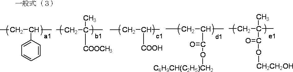
上記式中、a1、b1、c1、d1、およびe1は各モノマー単位のモル比率を表し、a1は3~60(モル%)、b1は30~95(モル%)、c1は0.5~25(モル%)、d1は0.5~40(モル%)、e1は1~10(モル%)を表す。
a1の好ましい範囲は上記xの好ましい範囲と同じであり、b1の好ましい範囲は上記yの好ましい範囲と同じであり、c1の好ましい範囲は上記zの好ましい範囲と同じであり、d1の好ましい範囲は上記wの好ましい範囲と同じである。
e1は1~10モル%であり、好ましくは2~9モル%であり、より好ましくは2~8モル%である。
a1の好ましい範囲は上記xの好ましい範囲と同じであり、b1の好ましい範囲は上記yの好ましい範囲と同じであり、c1の好ましい範囲は上記zの好ましい範囲と同じであり、d1の好ましい範囲は上記wの好ましい範囲と同じである。
e1は1~10モル%であり、好ましくは2~9モル%であり、より好ましくは2~8モル%である。
一般式(1)で表されるポリマーの具体例を以下に示すが、これらに限定されない。
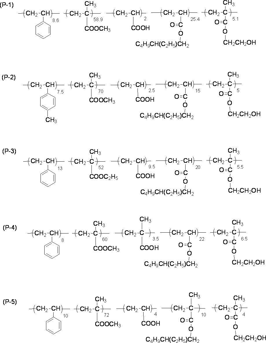
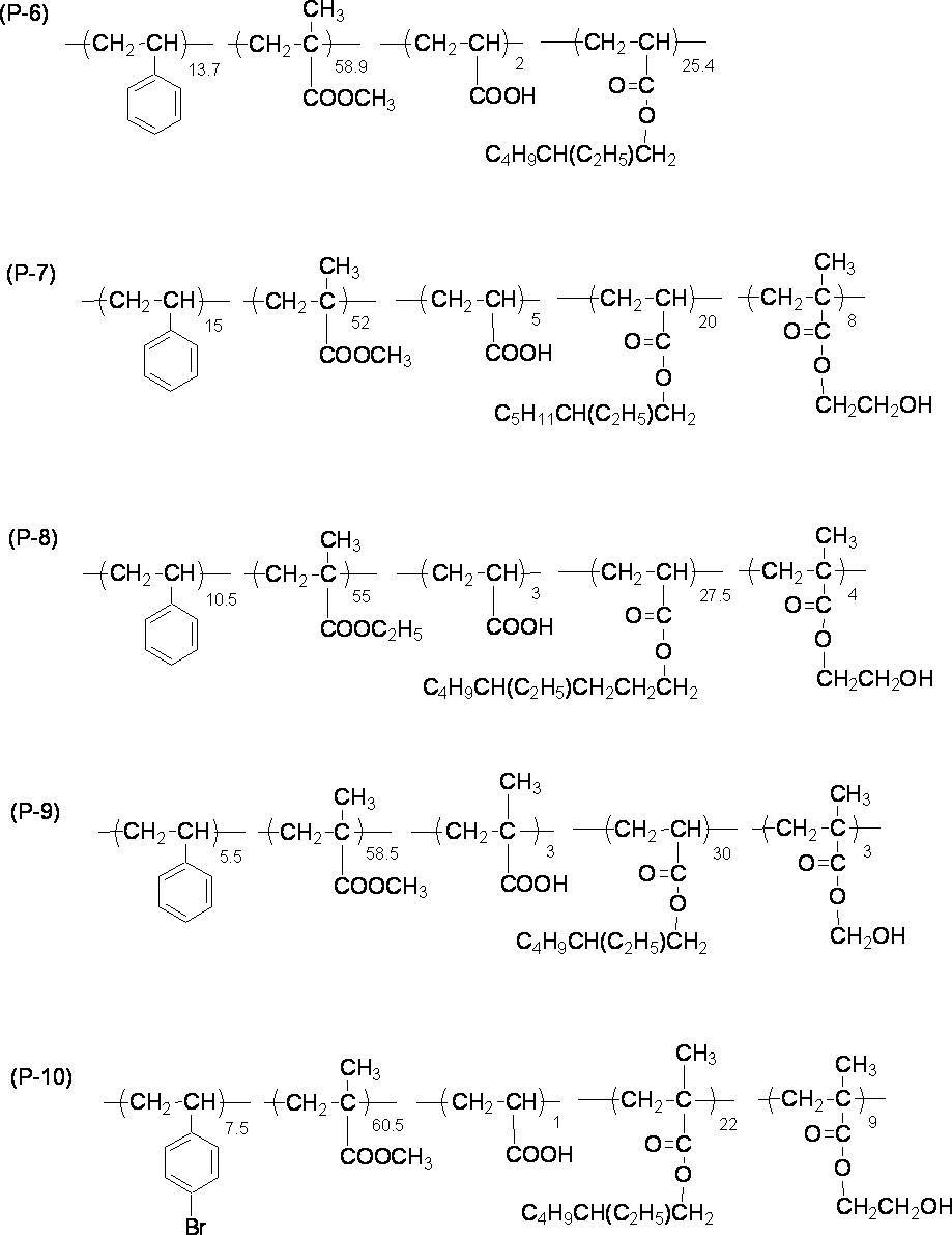
一般式(1)で表されるポリマーの重量平均分子量は、1000~100万が好ましく、2000~75万がより好ましく、3000~50万が更に好ましい。
一般式(1)で表されるポリマーは、例えば特許第3305459号及び特許第3754745号公報などを参照して合成することができる。
基板12上の第1引き出し配線16間(第2引き出し配線20間)間に、バインダー部がさらに配置されていてもよい。バインダー部が設けられることにより、第1引き出し配線16間(第2引き出し配線20間)のイオンマイグレーションがより抑制される。
バインダー部には、ゼラチンやゼラチンとは異なる高分子などが含まれ、好ましくはゼラチンが含まれる。
バインダー部には、ゼラチンやゼラチンとは異なる高分子などが含まれ、好ましくはゼラチンが含まれる。
バインダー部の厚みは特に制限されないが、導電性細線部の厚みより薄い場合が多い。
なお、バインダー部には、ゼラチンとは異なる高分子以外の成分が含まれていてもよい。
なお、バインダー部には、ゼラチンとは異なる高分子以外の成分が含まれていてもよい。
保護層22は、上記第1引き出し配線16および第2引き出し配線20を覆うように基板12上に配置される層である。保護層22を設けることにより、第1引き出し配線16間および第2引き出し配線20間のイオンマイグレーションが抑制される。なお、図3においては、第1引き出し配線16上に保護層22が配置された図を示すが、第2引き出し配線20上にも保護層22が配置される。
保護層22は、エポキシ樹脂を用いて形成される。使用されるエポキシ樹脂は特に制限されず、公知のエポキシ樹脂を使用することができる。例えば、グリシジルエーテル型エポキシ樹脂、グリシジルエステル型エポキシ樹脂、グリシジルアミン型エポキシ樹脂、酸化型エポキシ樹脂等を用いることができる。
グリシジルエーテル型エポキシ樹脂としては、ビスフェノールA型エポキシ樹脂、ビスフェノールF型エポキシ樹脂、ノボラック型エポキシ樹脂、アルコール型エポキシ樹脂等が挙げられる。また、グリシジルエステル型エポキシ樹脂としては、ヒドロフタル酸型エポキシ樹脂、ダイマー酸型エポキシ樹脂等が挙げられる。また、グリシジルアミン型エポキシ樹脂としては、芳香族アミン型エポキシ樹脂、アミノフェノール型エポキシ樹脂等が挙げられる。また、酸化型エポキシ樹脂としては、脂環型エポキシ樹脂等が挙げられる。さらにナフタレン骨格を有するエポキシ樹脂、フェノール骨格とビフェニル骨格を有するノボラック型エポキシ樹脂(ビフェニルノボラックエポキシ樹脂)、リン変性エポキシ樹脂等を用いることもできる。
保護層22は、エポキシ樹脂を用いて形成される。使用されるエポキシ樹脂は特に制限されず、公知のエポキシ樹脂を使用することができる。例えば、グリシジルエーテル型エポキシ樹脂、グリシジルエステル型エポキシ樹脂、グリシジルアミン型エポキシ樹脂、酸化型エポキシ樹脂等を用いることができる。
グリシジルエーテル型エポキシ樹脂としては、ビスフェノールA型エポキシ樹脂、ビスフェノールF型エポキシ樹脂、ノボラック型エポキシ樹脂、アルコール型エポキシ樹脂等が挙げられる。また、グリシジルエステル型エポキシ樹脂としては、ヒドロフタル酸型エポキシ樹脂、ダイマー酸型エポキシ樹脂等が挙げられる。また、グリシジルアミン型エポキシ樹脂としては、芳香族アミン型エポキシ樹脂、アミノフェノール型エポキシ樹脂等が挙げられる。また、酸化型エポキシ樹脂としては、脂環型エポキシ樹脂等が挙げられる。さらにナフタレン骨格を有するエポキシ樹脂、フェノール骨格とビフェニル骨格を有するノボラック型エポキシ樹脂(ビフェニルノボラックエポキシ樹脂)、リン変性エポキシ樹脂等を用いることもできる。
使用されるエポキシ樹脂のエポキシ当量は特に制限されないが、イオンマイグレーション抑制能がより優れる点で、100~1000000(g/eq)が好ましく、100~10000(g/eq)がより好ましい。
エポキシ樹脂の粘度(25℃)は特に制限されないが、溶媒への溶解性など取り扱い性がより優れる点から、1~1000Pa・sが好ましく、10~100Pa・sがより好ましい。なお、粘度は、エポキシ樹脂を25℃で保持した状態で、一般に用いられる粘度計(例えば、東機産業(株)製E型粘度計(RE-80L))を用いることにより測定される値である。
エポキシ樹脂の粘度(25℃)は特に制限されないが、溶媒への溶解性など取り扱い性がより優れる点から、1~1000Pa・sが好ましく、10~100Pa・sがより好ましい。なお、粘度は、エポキシ樹脂を25℃で保持した状態で、一般に用いられる粘度計(例えば、東機産業(株)製E型粘度計(RE-80L))を用いることにより測定される値である。
保護層を形成する際に、必要に応じて、エポキシ樹脂の硬化剤を使用してもよい。硬化剤の種類は特に制限されず、従来公知の硬化剤を使用することができる。例えば、イミダゾール系硬化剤、酸無水物系硬化剤、または、アミン系硬化剤(例えば、ポリアミドアミン)が挙げられる。
また、保護層にはフィラーが含まれていてもよい。フィラーの種類は特に制限されず、公知のフィラーを用いることができる。例えば、アルミニウム化合物、カルシウム化合物、カリウム化合物、マグネシウム化合物、ケイ素化合物、チタン化合物等からなるものが挙げられる。これらは単独で用いてもよいし、2種以上併用してもよい。
アルミニウム化合物としては、例えば、アルミナ、水酸化アルミニウム等が挙げられる。カルシウム化合物としては、例えば、炭酸カルシウム、水酸化カルシウム等が挙げられる。カリウム化合物としては、例えば、炭酸カリウム等が挙げられる。マグネシウム化合物としては、例えば、マグネシア、ドロマイト、塩基性炭酸マグネシウム、タルク等が挙げられる。ケイ素化合物としては、例えば、シリカ、ゼオライト等、チタン化合物としては酸化チタンが挙げられる。
また、保護層にはフィラーが含まれていてもよい。フィラーの種類は特に制限されず、公知のフィラーを用いることができる。例えば、アルミニウム化合物、カルシウム化合物、カリウム化合物、マグネシウム化合物、ケイ素化合物、チタン化合物等からなるものが挙げられる。これらは単独で用いてもよいし、2種以上併用してもよい。
アルミニウム化合物としては、例えば、アルミナ、水酸化アルミニウム等が挙げられる。カルシウム化合物としては、例えば、炭酸カルシウム、水酸化カルシウム等が挙げられる。カリウム化合物としては、例えば、炭酸カリウム等が挙げられる。マグネシウム化合物としては、例えば、マグネシア、ドロマイト、塩基性炭酸マグネシウム、タルク等が挙げられる。ケイ素化合物としては、例えば、シリカ、ゼオライト等、チタン化合物としては酸化チタンが挙げられる。
保護層22の厚みは特に制限されないが、引き出し配線間のイオンマイグレーションをより抑制できる点で、5~200μm以上が好ましく、外観形状を考慮すると10~100μm以上がより好ましい。
第1透明樹脂層40および第2透明樹脂層42は、それぞれ入力領域EIにある第1検出電極14上および第2検出電極18上に配置され、第1検出電極14と第1保護基板50との間、および、第2検出電極18と第2保護基板52との間の密着性を担保するための層(特に、粘着性透明樹脂層)である。
第1透明樹脂層40および第2透明樹脂層42の厚みは特に制限されないが、5~350μmであることが好ましく、20~150μmであることがさらに好ましい。上記範囲内であれば所望の可視光の透過率が得られ、且つ、取り扱いも容易である。
第1透明樹脂層40および第2透明樹脂層42の全光線透過率は、85~100%であることが好ましい。
第1透明樹脂層40および第2透明樹脂層42の厚みは特に制限されないが、5~350μmであることが好ましく、20~150μmであることがさらに好ましい。上記範囲内であれば所望の可視光の透過率が得られ、且つ、取り扱いも容易である。
第1透明樹脂層40および第2透明樹脂層42の全光線透過率は、85~100%であることが好ましい。
第1透明樹脂層40および第2透明樹脂層42を構成する材料としては、公知の粘着剤を使用することが好ましく、例えば、ゴム系粘着性絶縁材料、アクリル系粘着性絶縁材料、シリコーン系粘着性絶縁材料などが挙げられる。なかでも、透明性に優れる観点から、アクリル系粘着性絶縁材料であることが好ましい。
上記粘着性絶縁材料の好適態様であるアクリル系粘着性絶縁材料は、アルキル(メタ)アクリレート由来の繰り返し単位を有するアクリル系ポリマーを主成分としたものである。なお、(メタ)アクリレートは、アクリレートおよび/またはメタクリレートをいう。アクリル系粘着性絶縁材料のなかでも、粘着性がより優れる点から、アルキル基の炭素数が1~12程度であるアルキル(メタ)アクリレート由来の繰り返し単位を有するアクリル系ポリマーであることが好ましく、上記炭素数のアルキルメタクリレート由来の繰り返し単位および上記炭素数のアルキルアクリレート由来の繰り返し単位を有するアクリル系ポリマーがより好ましい。
上記アクリル系ポリマー中の繰り返し単位のなかには、(メタ)アクリル酸由来の繰り返し単位が含まれていてもよい。
上記粘着性絶縁材料の好適態様であるアクリル系粘着性絶縁材料は、アルキル(メタ)アクリレート由来の繰り返し単位を有するアクリル系ポリマーを主成分としたものである。なお、(メタ)アクリレートは、アクリレートおよび/またはメタクリレートをいう。アクリル系粘着性絶縁材料のなかでも、粘着性がより優れる点から、アルキル基の炭素数が1~12程度であるアルキル(メタ)アクリレート由来の繰り返し単位を有するアクリル系ポリマーであることが好ましく、上記炭素数のアルキルメタクリレート由来の繰り返し単位および上記炭素数のアルキルアクリレート由来の繰り返し単位を有するアクリル系ポリマーがより好ましい。
上記アクリル系ポリマー中の繰り返し単位のなかには、(メタ)アクリル酸由来の繰り返し単位が含まれていてもよい。
第1保護基板50および第2保護基板52は、それぞれ第1透明樹脂層40および第2透明樹脂層42上に配置される基板であり、外部環境から第1検出電極14や第2検出電極18を保護する基板であり、通常、一方の保護基板の主面はタッチ面を構成する。
第1保護基板50および第2保護基板52として、透明基板であることが好ましくプラスチックフィルム、プラスチック板、ガラス板等が用いられる。層の厚みはそれぞれの用途に応じて適宜選択することが望ましい。
上記プラスチックフィルムおよびプラスチック板の原料としては、例えば、ポリエチレンテレフタレート(PET)、ポリエチレンナフタレート(PEN)等のポリエステル類;ポリエチレン(PE)、ポリプロピレン(PP)、ポリスチレン、EVA等のポリオレフィン類;ビニル系樹脂;その他、ポリカーボネート(PC)、ポリアミド、ポリイミド、アクリル樹脂、トリアセチルセルロース(TAC)、シクロオレフィン系樹脂(COP)等を用いることができる。
また、第1保護基板50および第2保護基板52として、液晶ディスプレイや偏光板、円偏光板などを用いてもよい。
第1保護基板50および第2保護基板52として、透明基板であることが好ましくプラスチックフィルム、プラスチック板、ガラス板等が用いられる。層の厚みはそれぞれの用途に応じて適宜選択することが望ましい。
上記プラスチックフィルムおよびプラスチック板の原料としては、例えば、ポリエチレンテレフタレート(PET)、ポリエチレンナフタレート(PEN)等のポリエステル類;ポリエチレン(PE)、ポリプロピレン(PP)、ポリスチレン、EVA等のポリオレフィン類;ビニル系樹脂;その他、ポリカーボネート(PC)、ポリアミド、ポリイミド、アクリル樹脂、トリアセチルセルロース(TAC)、シクロオレフィン系樹脂(COP)等を用いることができる。
また、第1保護基板50および第2保護基板52として、液晶ディスプレイや偏光板、円偏光板などを用いてもよい。
なお、図1の外部導通領域Gには、図示しないフレキシブルプリント配線板が配置される。フレキシブルプリント配線板とは、基板上に複数の配線および端子が設けられた板であり、第1引き出し配線16のそれぞれの他端および第2引き出し配線20のそれぞれの他端に接続され、タッチパネル10と外部の装置(例えば、液晶表示装置)とを接続する役割を果たす。
次に、タッチパネル10が入力位置を検出する動作について説明する。
入力領域EIに対応する基板12の操作面上(第1保護基板50上)に、導電体である指が近接、接触、または押圧すると、指と第1検出電極14、第2検出電極18との間の静電容量が変化する。ここで、図示しない位置検出ドライバは、指と第1検出電極14、第2検出電極18との間の静電容量の変化を常に検出している。この位置検出ドライバは、所定値以上の静電容量の変化を検出すると、静電容量の変化が検出された位置を入力位置として検出する。このようにして、タッチパネル10は、入力位置を検出することができる。なお、タッチパネル10が入力位置を検出する方式として、相互キャパシタンス方式および自己キャパシタンス方式のいずれの方式であってもよい。相互キャパシタンス方式を採用すると、同時に複数の入力位置を検出できるので、自己キャパシタンス方式を採用する場合と比べて、好ましい。
なお、上記では、入力領域EIに対応する第1保護基板50を介して入力操作を行うタッチパネル10の例について説明したが、これに限定されない。すなわち、入力領域EIに対応する第1保護基板50を介して入力操作を行うタッチパネルであってもよい。
入力領域EIに対応する基板12の操作面上(第1保護基板50上)に、導電体である指が近接、接触、または押圧すると、指と第1検出電極14、第2検出電極18との間の静電容量が変化する。ここで、図示しない位置検出ドライバは、指と第1検出電極14、第2検出電極18との間の静電容量の変化を常に検出している。この位置検出ドライバは、所定値以上の静電容量の変化を検出すると、静電容量の変化が検出された位置を入力位置として検出する。このようにして、タッチパネル10は、入力位置を検出することができる。なお、タッチパネル10が入力位置を検出する方式として、相互キャパシタンス方式および自己キャパシタンス方式のいずれの方式であってもよい。相互キャパシタンス方式を採用すると、同時に複数の入力位置を検出できるので、自己キャパシタンス方式を採用する場合と比べて、好ましい。
なお、上記では、入力領域EIに対応する第1保護基板50を介して入力操作を行うタッチパネル10の例について説明したが、これに限定されない。すなわち、入力領域EIに対応する第1保護基板50を介して入力操作を行うタッチパネルであってもよい。
(タッチパネルの製造方法)
タッチパネル10の製造方法は特に制限されず、公知の方法を採用することができる。
まず、基板12上に第1検出電極14および第1引き出し配線16、並びに、第2検出電極18および第2引き出し配線20を形成する方法としては、ハロゲン化銀を使用した方法が挙げられる。より具体的には、基板12の両面にそれぞれ、ハロゲン化銀とゼラチンとを含有するハロゲン化銀乳剤層(以後、単に感光性層とも称する)を形成する工程(1)、感光性層を露光した後、現像処理することにより第1検出電極14および第1引き出し配線16、並びに、第2検出電極18および第2引き出し配線20を形成する工程(2)を有する方法が挙げられる。
以下に、各工程に関して説明する。
タッチパネル10の製造方法は特に制限されず、公知の方法を採用することができる。
まず、基板12上に第1検出電極14および第1引き出し配線16、並びに、第2検出電極18および第2引き出し配線20を形成する方法としては、ハロゲン化銀を使用した方法が挙げられる。より具体的には、基板12の両面にそれぞれ、ハロゲン化銀とゼラチンとを含有するハロゲン化銀乳剤層(以後、単に感光性層とも称する)を形成する工程(1)、感光性層を露光した後、現像処理することにより第1検出電極14および第1引き出し配線16、並びに、第2検出電極18および第2引き出し配線20を形成する工程(2)を有する方法が挙げられる。
以下に、各工程に関して説明する。
[工程(1):感光性層形成工程]
工程(1)は、基板12の両面に、ハロゲン化銀とゼラチンとを含有する感光性層を形成する工程である。
感光性層を形成する方法は特に制限されないが、生産性の点から、ハロゲン化銀およびバインダーを含有する感光性層形成用組成物を基板12に接触させ、基板12の両面上に感光性層を形成する方法が好ましい。
以下に、上記方法で使用される感光性層形成用組成物の態様について詳述した後、工程の手順について詳述する。
工程(1)は、基板12の両面に、ハロゲン化銀とゼラチンとを含有する感光性層を形成する工程である。
感光性層を形成する方法は特に制限されないが、生産性の点から、ハロゲン化銀およびバインダーを含有する感光性層形成用組成物を基板12に接触させ、基板12の両面上に感光性層を形成する方法が好ましい。
以下に、上記方法で使用される感光性層形成用組成物の態様について詳述した後、工程の手順について詳述する。
感光性層形成用組成物には、ハロゲン化銀およびゼラチンが含有される。
ハロゲン化銀に含有されるハロゲン元素は、塩素、臭素、ヨウ素およびフッ素のいずれであってもよく、これらを組み合わせでもよい。ハロゲン化銀としては、例えば、塩化銀、臭化銀、ヨウ化銀を主体としたハロゲン化銀が好ましく用いられ、更に臭化銀や塩化銀を主体としたハロゲン化銀が好ましく用いられる。
ゼラチンの種類は、上述の通りである。
感光性層形成用組成物中に含まれるハロゲン化銀およびゼラチンの体積比は特に制限されず、上述した導電性細線30中における金属とバインダーとの好適な体積比の範囲となるように適宜調整される。
ハロゲン化銀に含有されるハロゲン元素は、塩素、臭素、ヨウ素およびフッ素のいずれであってもよく、これらを組み合わせでもよい。ハロゲン化銀としては、例えば、塩化銀、臭化銀、ヨウ化銀を主体としたハロゲン化銀が好ましく用いられ、更に臭化銀や塩化銀を主体としたハロゲン化銀が好ましく用いられる。
ゼラチンの種類は、上述の通りである。
感光性層形成用組成物中に含まれるハロゲン化銀およびゼラチンの体積比は特に制限されず、上述した導電性細線30中における金属とバインダーとの好適な体積比の範囲となるように適宜調整される。
感光性層形成用組成物には、必要に応じて、溶媒が含有される。
使用される溶媒としては、例えば、水、有機溶媒(例えば、メタノール等のアルコール類、アセトン等のケトン類、ホルムアミド等のアミド類、ジメチルスルホキシド等のスルホキシド類、酢酸エチル等のエステル類、エーテル類等)、イオン性液体、またはこれらの混合溶媒を挙げることができる。
使用される溶媒の含有量は特に制限されないが、ハロゲン化銀およびバインダーの合計質量に対して、30~90質量%の範囲が好ましく、50~80質量%の範囲がより好ましい。
使用される溶媒としては、例えば、水、有機溶媒(例えば、メタノール等のアルコール類、アセトン等のケトン類、ホルムアミド等のアミド類、ジメチルスルホキシド等のスルホキシド類、酢酸エチル等のエステル類、エーテル類等)、イオン性液体、またはこれらの混合溶媒を挙げることができる。
使用される溶媒の含有量は特に制限されないが、ハロゲン化銀およびバインダーの合計質量に対して、30~90質量%の範囲が好ましく、50~80質量%の範囲がより好ましい。
感光性層形成用組成物には、必要に応じて、上述した材料以外の他の材料が含まれていてもよい。例えば、ハロゲン化銀の安定化および高感度化のために用いられるロジウム化合物、イリジウム化合物などのVIII族、VIIB族に属する金属化合物が挙げられる。または、特開2009-004348号公報の段落[0220]~[0241]に記載されるような、帯電防止剤、造核促進剤、分光増感色素、界面活性剤、カブリ防止剤、硬膜剤、黒ポツ防止剤、レドックス化合物、モノメチン化合物、ジヒドロキシベンゼン類などが挙げられる。さらには、物理現像核が含まれていてもよい。
なかでも、ハロゲン化銀含有感光性層には、上記高分子同士を架橋するために使用される架橋剤が含まれることが好ましい。架橋剤が含まれることにより、高分子同士間での架橋が進行し、導電部中の金属銀同士の連結が保たれ、結果として導電特性に優れた導電膜が得られる。
使用される架橋剤の種類は特に制限されず、使用される高分子の構造に応じて適宜最適な架橋剤が選択される。通常、架橋剤は、高分子中に含まれる基(反応性基)と反応する架橋性基を少なくとも2つ有する。
例えば、上記高分子中の反応性基と、架橋剤中の架橋性基との好適な組み合わせとしては、反応性がより優れる点で、例えば、以下の(1)~(8)の組み合わせが挙げられる。
(1)水酸基とイソシアネート基
(2)カルボン酸基とエポキシ基
(3)水酸基とカルボン酸無水物基
(4)カルボン酸基とイソシアネート基
(5)アミノ基とイソシアネート基
(6)水酸基とエポキシ基
(7)アミノ基とエポキシ基
(8)アミノ基とハロゲン化アルキル基
使用される架橋剤の種類は特に制限されず、使用される高分子の構造に応じて適宜最適な架橋剤が選択される。通常、架橋剤は、高分子中に含まれる基(反応性基)と反応する架橋性基を少なくとも2つ有する。
例えば、上記高分子中の反応性基と、架橋剤中の架橋性基との好適な組み合わせとしては、反応性がより優れる点で、例えば、以下の(1)~(8)の組み合わせが挙げられる。
(1)水酸基とイソシアネート基
(2)カルボン酸基とエポキシ基
(3)水酸基とカルボン酸無水物基
(4)カルボン酸基とイソシアネート基
(5)アミノ基とイソシアネート基
(6)水酸基とエポキシ基
(7)アミノ基とエポキシ基
(8)アミノ基とハロゲン化アルキル基
架橋剤としては、ビニルスルホン類(例えば1,3-ビスビニルスルホニルプロパン)、アルデヒド類(例えばグリオキサール)、塩化ピリミジン類(例えば2,4,6-トリクロロピリミジン)、塩化トリアジン類(例えば塩化シアヌル)、エポキシ化合物、カルボジイミド化合物等が挙げられる。なお、光照射により誘起される光化学反応を利用して架橋反応が進行する架橋剤であってもよい。
(工程の手順)
感光性層形成用組成物と基板12とを接触させる方法は特に制限されず、公知の方法を採用できる。例えば、感光性層形成用組成物を基板12に塗布する方法や、感光性層形成用組成物中に基板12を浸漬する方法などが挙げられる。
感光性層中におけるハロゲン化銀の含有量は特に制限されないが、導電特性がより優れる点で、銀換算で1.0~20.0g/m2が好ましく、5.0~15.0g/m2がより好ましい。
感光性層形成用組成物と基板12とを接触させる方法は特に制限されず、公知の方法を採用できる。例えば、感光性層形成用組成物を基板12に塗布する方法や、感光性層形成用組成物中に基板12を浸漬する方法などが挙げられる。
感光性層中におけるハロゲン化銀の含有量は特に制限されないが、導電特性がより優れる点で、銀換算で1.0~20.0g/m2が好ましく、5.0~15.0g/m2がより好ましい。
なお、必要に応じて、感光性層上にバインダーからなる保護層をさらに設けてもよい。保護層を設けることにより、擦り傷防止や力学特性の改良がなされる。
[工程(2):露光現像工程]
工程(2)は、上記工程(1)で得られた感光性層をパターン露光した後、現像処理することにより第1検出電極14および第1引き出し配線16、並びに、第2検出電極18および第2引き出し配線20を形成する工程である。
まず、以下では、パターン露光処理について詳述し、その後現像処理について詳述する。
工程(2)は、上記工程(1)で得られた感光性層をパターン露光した後、現像処理することにより第1検出電極14および第1引き出し配線16、並びに、第2検出電極18および第2引き出し配線20を形成する工程である。
まず、以下では、パターン露光処理について詳述し、その後現像処理について詳述する。
(パターン露光)
感光性層に対してパターン状の露光を施すことにより、露光領域における感光性層中のハロゲン化銀が潜像を形成する。この潜像が形成された領域は、後述する現像処理によって第1検出電極14および第1引き出し配線16、並びに、第2検出電極18および第2引き出し配線20を形成する。一方、露光がなされなかった未露光領域では、後述する定着処理の際にハロゲン化銀が溶解して感光性層から流出し、透明な膜が得られる。
露光の際に使用される光源は特に制限されず、可視光線、紫外線などの光、または、X線などの放射線などが挙げられる。
パターン露光を行う方法は特に制限されず、例えば、フォトマスクを利用した面露光で行ってもよいし、レーザービームによる走査露光で行ってもよい。なお、パターンの形状は特に制限されず、形成したい導電性細線のパターンに合わせて適宜調整される。
感光性層に対してパターン状の露光を施すことにより、露光領域における感光性層中のハロゲン化銀が潜像を形成する。この潜像が形成された領域は、後述する現像処理によって第1検出電極14および第1引き出し配線16、並びに、第2検出電極18および第2引き出し配線20を形成する。一方、露光がなされなかった未露光領域では、後述する定着処理の際にハロゲン化銀が溶解して感光性層から流出し、透明な膜が得られる。
露光の際に使用される光源は特に制限されず、可視光線、紫外線などの光、または、X線などの放射線などが挙げられる。
パターン露光を行う方法は特に制限されず、例えば、フォトマスクを利用した面露光で行ってもよいし、レーザービームによる走査露光で行ってもよい。なお、パターンの形状は特に制限されず、形成したい導電性細線のパターンに合わせて適宜調整される。
(現像処理)
現像処理の方法は特に制限されないが、例えば、感光性層の種類に応じて以下の3通りの方式から選択することができる。
(1)物理現像核を含まない感光性層を化学現像または熱現像して金属銀を形成させる方式。
(2)物理現像核を含む感光性層を溶解物理現像して金属銀を形成させる方式。
(3)物理現像核を含まない感光性層と、物理現像核を含む非感光性層を有する受像シートを重ね合わせて拡散転写現像して金属銀を形成させる方式。
現像処理の方法は特に制限されないが、例えば、感光性層の種類に応じて以下の3通りの方式から選択することができる。
(1)物理現像核を含まない感光性層を化学現像または熱現像して金属銀を形成させる方式。
(2)物理現像核を含む感光性層を溶解物理現像して金属銀を形成させる方式。
(3)物理現像核を含まない感光性層と、物理現像核を含む非感光性層を有する受像シートを重ね合わせて拡散転写現像して金属銀を形成させる方式。
ここでいう化学現像、熱現像、溶解物理現像、および拡散転写現像は、当業界で通常用いられている用語どおりの意味であり、写真化学の一般教科書、例えば菊地真一著「写真化学」(共立出版社刊行)、C.E.K.Mees編「The Theory of Photographic Process,4th ed.」(Mcmillan社、1977年刊行)に解説されている。また、例えば、特開2004-184693号公報、同2004-334077号公報、同2005-010752号公報等に記載の技術を参照することもできる。
上記の(1)~(3)の方式の中で、方式(1)が、現像前の感光性層に物理現像核を有さないこと、2シートの拡散転写方式でないことから、方式(1)が最も簡便、安定な処理ができ、本発明の導電シートの製造には好ましい。以下、方式(1)での説明を記載するが、他の方式を用いる場合には上段記載の文献を参照することができる。なお、”溶解物理現像”は、方式(2)にのみ固有な現像法ではなく、方式(1)でも利用できる現像方法である。
現像処理の方法は特に制限されず、公知の方法を採用できる。例えば、銀塩写真フィルム、印画紙、印刷製版用フィルム、フォトマスク用エマルジョンマスク等に用いられる通常の現像処理の技術を用いることができる。
現像処理の際に使用される現像液の種類は特に制限されないが、例えば、PQ現像液、MQ現像液、MAA現像液等を用いることもできる。市販品では、例えば、富士フイルム社処方のCN-16、CR-56、CP45X、FD-3、パピトール、KODAK社処方のC-41、E-6、RA-4、D-19、D-72等の現像液、又はそのキットに含まれる現像液を用いることができる。また、リス現像液を用いることもできる。
現像処理は、未露光部分の銀塩を除去して安定化させる目的で行われる定着処理を含むことができる。定着処理は、銀塩写真フィルムや印画紙、印刷製版用フィルム、フォトマスク用エマルジョンマスク等に用いられる定着処理の技術を用いることができる。
定着工程における定着温度は、約20℃~約50℃が好ましく、25~45℃がより好ましい。また、定着時間は5秒~1分が好ましく、7秒~50秒がより好ましい。
現像処理後の露光部(導電性細線)に含まれる金属銀の質量は、露光前の露光部に含まれていた銀の質量に対して50質量%以上の含有率であることが好ましく、80質量%以上であることが更に好ましい。露光部に含まれる銀の質量が露光前の露光部に含まれていた銀の質量に対して50質量%以上であれば、高い導電性を得ることができるため好ましい。
現像処理の際に使用される現像液の種類は特に制限されないが、例えば、PQ現像液、MQ現像液、MAA現像液等を用いることもできる。市販品では、例えば、富士フイルム社処方のCN-16、CR-56、CP45X、FD-3、パピトール、KODAK社処方のC-41、E-6、RA-4、D-19、D-72等の現像液、又はそのキットに含まれる現像液を用いることができる。また、リス現像液を用いることもできる。
現像処理は、未露光部分の銀塩を除去して安定化させる目的で行われる定着処理を含むことができる。定着処理は、銀塩写真フィルムや印画紙、印刷製版用フィルム、フォトマスク用エマルジョンマスク等に用いられる定着処理の技術を用いることができる。
定着工程における定着温度は、約20℃~約50℃が好ましく、25~45℃がより好ましい。また、定着時間は5秒~1分が好ましく、7秒~50秒がより好ましい。
現像処理後の露光部(導電性細線)に含まれる金属銀の質量は、露光前の露光部に含まれていた銀の質量に対して50質量%以上の含有率であることが好ましく、80質量%以上であることが更に好ましい。露光部に含まれる銀の質量が露光前の露光部に含まれていた銀の質量に対して50質量%以上であれば、高い導電性を得ることができるため好ましい。
上記で形成された第1引き出し配線16および第2引き出し配線20上に保護層22を形成する方法は特に制限されず、例えば、上述したエポキシ樹脂を含む保護層形成用樹脂組成物を第1引き出し配線16および第2引き出し配線20上に塗布して、硬化処理を施すことにより、保護層22を製造することができる。
保護層形成用樹脂組成物中に含まれるエポキシ樹脂の定義は上述の通りである。
また、必要に応じて、保護層形成用樹脂組成物には、エポキシ樹脂以外の成分(例えば、硬化剤、フィラー、溶媒、酸発生剤など)が含まれていてもよい。
保護層形成用樹脂組成物を塗布する方法は特に制限されず、例えば、インクジェット法、スクリーン印刷法、ディスペンサー法などが挙げられる。
また、硬化処理の方法は特に制限されず、加熱処理や光照射処理が挙げられ、硬化の程度がより優れる点で、加熱処理が好ましい。
加熱処理の条件は特に制限されず、使用されるエポキシ樹脂の種類に応じて、最適な条件が適宜選択される。通常、基板の耐熱性などの点から、40~150℃(好ましくは、50~120℃)で2時間以下(好ましくは、0.2時間~1時間以内)加熱処理を施すことが好ましい。
保護層形成用樹脂組成物中に含まれるエポキシ樹脂の定義は上述の通りである。
また、必要に応じて、保護層形成用樹脂組成物には、エポキシ樹脂以外の成分(例えば、硬化剤、フィラー、溶媒、酸発生剤など)が含まれていてもよい。
保護層形成用樹脂組成物を塗布する方法は特に制限されず、例えば、インクジェット法、スクリーン印刷法、ディスペンサー法などが挙げられる。
また、硬化処理の方法は特に制限されず、加熱処理や光照射処理が挙げられ、硬化の程度がより優れる点で、加熱処理が好ましい。
加熱処理の条件は特に制限されず、使用されるエポキシ樹脂の種類に応じて、最適な条件が適宜選択される。通常、基板の耐熱性などの点から、40~150℃(好ましくは、50~120℃)で2時間以下(好ましくは、0.2時間~1時間以内)加熱処理を施すことが好ましい。
第1透明樹脂層40および第2透明樹脂層42を形成する方法は特に制限されず、公知の透明樹脂フィルムを張り合わせる方法や、透明樹脂層を形成する透明樹脂層形成用組成物を塗布して層を形成する方法などが挙げられる。
第1保護基板50および第2保護基板52を形成する方法は特に制限されず、第1透明樹脂層40および第2透明樹脂層42上にそれぞれ保護基板を張り合わせる方法が挙げられる。
上記においては、第1検出電極および第2検出電極が基板の表面および裏面に配置される態様について詳述したが、本発明のタッチパネルはこの態様には限定されない。
以下に、本発明のタッチパネルの別態様について詳述する。
以下に、本発明のタッチパネルの別態様について詳述する。
<第2の実施態様>
図5に、本発明のタッチパネルの第2の実施形態の一部の断面図を示す。なお、図5は、タッチパネル200の層構成に対する理解を容易にするために模式的に表したものであり、一部を省略している。
図5に示すように、タッチパネル200は、第2基板62と、第2基板62上に配置された第2検出電極18と、第2検出電極18の一端に電気的に接続し、第2基板62上に配置された第2引き出し配線(図示せず)と、第2透明樹脂層42と、第1検出電極14と、第1検出電極14の一端に電気的に接続している第1引き出し配線16(図示せず)と、第1検出電極14および第1引き出し配線16が隣接する第1基板60と、第1透明樹脂層40と、第1保護基板50と、第1引き出し配線および第2引き出し配線を覆う保護層(図示しない)を備える。
図5に示すタッチパネル200は、各層の順番が異なる点を除いて、図1に示すタッチパネル10と同様の層を有するものであるので、同一の構成要素には同一の参照符号を付し、その説明を省略する。なお、第1基板60および第2基板62は、図1に示す基板12と同様の層であり、その定義は上述の通りである。
また、図5中の第1検出電極14と第2検出電極18とは、図1に示すようにそれぞれ複数使用されており、両者は図1に示すように互いに直交するように配置されている。
なお、図5に示す、タッチパネル200は、基板と基板表面に配置された検出電極および引き出し配線とを有する電極付き基板を2枚用意し、電極同士が向き合うように、透明樹脂層を介して貼り合せて得られるタッチパネルに該当する。
図5に、本発明のタッチパネルの第2の実施形態の一部の断面図を示す。なお、図5は、タッチパネル200の層構成に対する理解を容易にするために模式的に表したものであり、一部を省略している。
図5に示すように、タッチパネル200は、第2基板62と、第2基板62上に配置された第2検出電極18と、第2検出電極18の一端に電気的に接続し、第2基板62上に配置された第2引き出し配線(図示せず)と、第2透明樹脂層42と、第1検出電極14と、第1検出電極14の一端に電気的に接続している第1引き出し配線16(図示せず)と、第1検出電極14および第1引き出し配線16が隣接する第1基板60と、第1透明樹脂層40と、第1保護基板50と、第1引き出し配線および第2引き出し配線を覆う保護層(図示しない)を備える。
図5に示すタッチパネル200は、各層の順番が異なる点を除いて、図1に示すタッチパネル10と同様の層を有するものであるので、同一の構成要素には同一の参照符号を付し、その説明を省略する。なお、第1基板60および第2基板62は、図1に示す基板12と同様の層であり、その定義は上述の通りである。
また、図5中の第1検出電極14と第2検出電極18とは、図1に示すようにそれぞれ複数使用されており、両者は図1に示すように互いに直交するように配置されている。
なお、図5に示す、タッチパネル200は、基板と基板表面に配置された検出電極および引き出し配線とを有する電極付き基板を2枚用意し、電極同士が向き合うように、透明樹脂層を介して貼り合せて得られるタッチパネルに該当する。
<第3の実施態様>
図6に、本発明のタッチパネルの第3の実施形態の一部の断面図を示す。なお、図6は、タッチパネル300の層構成に対する理解を容易にするために模式的に表したものであり、一部を省略している。
図6に示すように、タッチパネル300は、第2基板62と、第2基板62上に配置された第2検出電極18と、第2検出電極18の一端に電気的に接続し、第2基板62上に配置された第2引き出し配線(図示せず)と、第2透明樹脂層42と、第1基板60と、第1基板60上に配置された第1検出電極14と、第1検出電極14の一端に電気的に接続し、第1基板60上に配置された第1引き出し配線(図示せず)と、第1透明樹脂層40と、第1保護基板50と、第1引き出し配線および第2引き出し配線を覆う保護層(図示しない)を備える。
図6に示すタッチパネル300は、各層の順番が異なる点を除いて、図1に示すタッチパネル10と同様の層を有するものであるので、同一の構成要素には同一の参照符号を付し、その説明を省略する。
また、図6中の第1検出電極14と第2検出電極18とは、図1に示すようにそれぞれ複数使用されており、両者は図1に示すように互いに直交するように配置されている。
なお、図6に示す、タッチパネル300は、基板と基板表面に配置された検出電極および引き出し配線とを有する電極付き基板を2枚用意し、一方の電極付き基板中の基板と他方の電極付き基板の電極とが向き合うように、透明樹脂層を介して貼り合せて得られるタッチパネルに該当する。
図6に、本発明のタッチパネルの第3の実施形態の一部の断面図を示す。なお、図6は、タッチパネル300の層構成に対する理解を容易にするために模式的に表したものであり、一部を省略している。
図6に示すように、タッチパネル300は、第2基板62と、第2基板62上に配置された第2検出電極18と、第2検出電極18の一端に電気的に接続し、第2基板62上に配置された第2引き出し配線(図示せず)と、第2透明樹脂層42と、第1基板60と、第1基板60上に配置された第1検出電極14と、第1検出電極14の一端に電気的に接続し、第1基板60上に配置された第1引き出し配線(図示せず)と、第1透明樹脂層40と、第1保護基板50と、第1引き出し配線および第2引き出し配線を覆う保護層(図示しない)を備える。
図6に示すタッチパネル300は、各層の順番が異なる点を除いて、図1に示すタッチパネル10と同様の層を有するものであるので、同一の構成要素には同一の参照符号を付し、その説明を省略する。
また、図6中の第1検出電極14と第2検出電極18とは、図1に示すようにそれぞれ複数使用されており、両者は図1に示すように互いに直交するように配置されている。
なお、図6に示す、タッチパネル300は、基板と基板表面に配置された検出電極および引き出し配線とを有する電極付き基板を2枚用意し、一方の電極付き基板中の基板と他方の電極付き基板の電極とが向き合うように、透明樹脂層を介して貼り合せて得られるタッチパネルに該当する。
本発明のタッチパネルを含む入力装置の構成は特に制限されないが、例えば、図7に示す態様が挙げられる。図7に示す態様はいわゆるアウトセル型の態様に該当し、バックライト110と、第1偏光板120と、液晶ディスプレイ(LCD)130と、第2偏光板140と、本発明のタッチパネル150と、保護基板160とをこの順で含む入力装置170aが挙げられる。なお、第2偏光板140とタッチパネル150との間は、図示しないスペーサーが配置されている。
また、入力装置の態様としては図7の態様に限定されず、例えば、図8に示す、バックライト110と、第1偏光板120と、液晶ディスプレイ(LCD)130と、第2偏光板140と、粘着層180と、本発明のタッチパネル150と、保護基板160とをこの順で含む入力装置170bが挙げられる。
さらに、入力装置の別態様としては、図9に示す、バックライト110と、第1偏光板120と、液晶ディスプレイ(LCD)130と、本発明のタッチパネル150と、第2偏光板140と、保護基板160とをこの順で含む入力装置170cが挙げられる。
また、入力装置の態様としては図7の態様に限定されず、例えば、図8に示す、バックライト110と、第1偏光板120と、液晶ディスプレイ(LCD)130と、第2偏光板140と、粘着層180と、本発明のタッチパネル150と、保護基板160とをこの順で含む入力装置170bが挙げられる。
さらに、入力装置の別態様としては、図9に示す、バックライト110と、第1偏光板120と、液晶ディスプレイ(LCD)130と、本発明のタッチパネル150と、第2偏光板140と、保護基板160とをこの順で含む入力装置170cが挙げられる。
本発明のタッチパネル(静電容量式タッチパネル)は、上述の実施の形態に限らず、本発明の要旨を逸脱することなく、種々の構成を採り得ることはもちろんである。また、特開2011-113149号公報、特開2011-129501号公報、特開2011-129112号公報、特開2011-134311号公報、特開2011-175628号公報などに開示の技術と適宜組み合わせて使用することができる。
以下、実施例により、本発明について更に詳細に説明するが、本発明はこれらに限定されるものではない。
<実施例A>
<実施例1>
(ハロゲン化銀乳剤の調製)
38℃、pH4.5に保たれた下記1液に、下記の2液および3液の各々90%に相当する量を攪拌しながら同時に20分間にわたって加え、0.16μmの核粒子を形成した。続いて下記4液および5液を8分間にわたって加え、更に、下記の2液および3液の残りの10%の量を2分間にわたって加え、0.21μmまで成長させた。更に、ヨウ化カリウム0.15gを加え、5分間熟成し粒子形成を終了した。
<実施例1>
(ハロゲン化銀乳剤の調製)
38℃、pH4.5に保たれた下記1液に、下記の2液および3液の各々90%に相当する量を攪拌しながら同時に20分間にわたって加え、0.16μmの核粒子を形成した。続いて下記4液および5液を8分間にわたって加え、更に、下記の2液および3液の残りの10%の量を2分間にわたって加え、0.21μmまで成長させた。更に、ヨウ化カリウム0.15gを加え、5分間熟成し粒子形成を終了した。
1液:
水 750ml
ゼラチン 9g
塩化ナトリウム 3g
1,3-ジメチルイミダゾリジン-2-チオン 20mg
ベンゼンチオスルホン酸ナトリウム 10mg
クエン酸 0.7g
2液:
水 300ml
硝酸銀 150g
3液:
水 300ml
塩化ナトリウム 38g
臭化カリウム 32g
ヘキサクロロイリジウム(III)酸カリウム
(0.005%KCl 20%水溶液) 8ml
ヘキサクロロロジウム酸アンモニウム
(0.001%NaCl 20%水溶液) 10ml
4液:
水 100ml
硝酸銀 50g
5液:
水 100ml
塩化ナトリウム 13g
臭化カリウム 11g
黄血塩 5mg
水 750ml
ゼラチン 9g
塩化ナトリウム 3g
1,3-ジメチルイミダゾリジン-2-チオン 20mg
ベンゼンチオスルホン酸ナトリウム 10mg
クエン酸 0.7g
2液:
水 300ml
硝酸銀 150g
3液:
水 300ml
塩化ナトリウム 38g
臭化カリウム 32g
ヘキサクロロイリジウム(III)酸カリウム
(0.005%KCl 20%水溶液) 8ml
ヘキサクロロロジウム酸アンモニウム
(0.001%NaCl 20%水溶液) 10ml
4液:
水 100ml
硝酸銀 50g
5液:
水 100ml
塩化ナトリウム 13g
臭化カリウム 11g
黄血塩 5mg
その後、常法に従い、フロキュレーション法によって水洗した。具体的には、温度を35℃に下げ、硫酸を用いてハロゲン化銀が沈降するまでpHを下げた(pH3.6±0.2の範囲であった)。次に、上澄み液を約3リットル除去した(第一水洗)。更に3リットルの蒸留水を加えてから、ハロゲン化銀が沈降するまで硫酸を加えた。再度、上澄み液を3リットル除去した(第二水洗)。第二水洗と同じ操作を更に1回繰り返して(第三水洗)、水洗・脱塩工程を終了した。水洗・脱塩後の乳剤をpH6.4、pAg7.5に調整し、ゼラチン3.9g、ベンゼンチオスルホン酸ナトリウム10mg、ベンゼンチオスルフィン酸ナトリウム3mg、チオ硫酸ナトリウム15mgと塩化金酸10mgを加え55℃にて最適感度を得るように化学増感を施し、安定剤として1,3,3a,7-テトラアザインデン100mg、防腐剤としてプロキセル(商品名、ICI Co.,Ltd.製)100mgを加えた。最終的に得られた乳剤は、沃化銀を0.08モル%含み、塩臭化銀の比率を塩化銀70モル%、臭化銀30モル%とする、平均粒子径0.22μm、変動係数9%のヨウ塩臭化銀立方体粒子乳剤であった。
(感光性層形成用組成物の調製)
上記乳剤に1,3,3a,7-テトラアザインデン1.2×10⁻⁴モル/モルAg、ハイドロキノン1.2×10-2モル/モルAg、クエン酸3.0×10-4モル/モルAg、2,4-ジクロロ-6-ヒドロキシ-1,3,5-トリアジンナトリウム塩0.90g/モルAgを添加し、クエン酸を用いて塗布液pHを5.6に調整して、感光性層形成用組成物を得た。
上記乳剤に1,3,3a,7-テトラアザインデン1.2×10⁻⁴モル/モルAg、ハイドロキノン1.2×10-2モル/モルAg、クエン酸3.0×10-4モル/モルAg、2,4-ジクロロ-6-ヒドロキシ-1,3,5-トリアジンナトリウム塩0.90g/モルAgを添加し、クエン酸を用いて塗布液pHを5.6に調整して、感光性層形成用組成物を得た。
(感光性層形成工程)
厚み100μmのポリエチレンテレフタレート(PET)フィルムにコロナ放電処理を施した後、上記PETフィルムの両面に、下塗層として厚み0.1μmのゼラチン層、さらに下塗層上に光学濃度が約1.0で現像液のアルカリにより脱色する染料を含むアンチハレーション層を設けた。上記アンチハレーション層の上に、上記感光性層形成用組成物を塗布し、さらに厚み0.15μmのゼラチン層を設け、両面に感光性層が形成されたPETフィルムを得た。得られたフィルムをフィルムAとする。形成された感光性層は、銀量6.0g/m2、ゼラチン量1.0g/m2であった。
厚み100μmのポリエチレンテレフタレート(PET)フィルムにコロナ放電処理を施した後、上記PETフィルムの両面に、下塗層として厚み0.1μmのゼラチン層、さらに下塗層上に光学濃度が約1.0で現像液のアルカリにより脱色する染料を含むアンチハレーション層を設けた。上記アンチハレーション層の上に、上記感光性層形成用組成物を塗布し、さらに厚み0.15μmのゼラチン層を設け、両面に感光性層が形成されたPETフィルムを得た。得られたフィルムをフィルムAとする。形成された感光性層は、銀量6.0g/m2、ゼラチン量1.0g/m2であった。
(露光現像工程)
上記フィルムAの両面に、図1に示すような、タッチパネルセンサーパターン(第1検出電極および第2検出電極)および引き出し配線部(第1引き出し配線および第2引き出し配線)を配したフォトマスクを介し、高圧水銀ランプを光源とした平行光を用いて露光を行った。露光後、下記の現像液で現像し、更に定着液(商品名:CN16X用N3X-R、富士フィルム社製)を用いて現像処理を行った。さらに、純水でリンスし、乾燥することで、両面にAg細線からなる電極パターンとゼラチン層とが形成されたPETフィルムを得た。ゼラチン層はAg細線間に形成されていた。得られたフィルムをフィルムBとする。なお、引き出し配線部のL/S(ライン/スペース)は100μm/100μmであった。
上記フィルムAの両面に、図1に示すような、タッチパネルセンサーパターン(第1検出電極および第2検出電極)および引き出し配線部(第1引き出し配線および第2引き出し配線)を配したフォトマスクを介し、高圧水銀ランプを光源とした平行光を用いて露光を行った。露光後、下記の現像液で現像し、更に定着液(商品名:CN16X用N3X-R、富士フィルム社製)を用いて現像処理を行った。さらに、純水でリンスし、乾燥することで、両面にAg細線からなる電極パターンとゼラチン層とが形成されたPETフィルムを得た。ゼラチン層はAg細線間に形成されていた。得られたフィルムをフィルムBとする。なお、引き出し配線部のL/S(ライン/スペース)は100μm/100μmであった。
(現像液の組成)
現像液1リットル(L)中に、以下の化合物が含まれる。
ハイドロキノン 0.037mol/L
N-メチルアミノフェノール 0.016mol/L
メタホウ酸ナトリウム 0.140mol/L
水酸化ナトリウム 0.360mol/L
臭化ナトリウム 0.031mol/L
メタ重亜硫酸カリウム 0.187mol/L
現像液1リットル(L)中に、以下の化合物が含まれる。
ハイドロキノン 0.037mol/L
N-メチルアミノフェノール 0.016mol/L
メタホウ酸ナトリウム 0.140mol/L
水酸化ナトリウム 0.360mol/L
臭化ナトリウム 0.031mol/L
メタ重亜硫酸カリウム 0.187mol/L
上記で得られたフィルムBの引き出し配線部(第1引き出し配線および第2引き出し配線)上に、エポキシ樹脂組成物(LPD-200、ヘンケル製)をディスペンサーにより塗布して、その後、80℃で0.5時間加熱処理を施し、保護層(厚み:100μm)を製造した。
なお、上記エポキシ樹脂組成物には、無機フィラーが含まれる。
なお、上記エポキシ樹脂組成物には、無機フィラーが含まれる。
上記で得られたフィルムBの一方の面上(ボトム面)に3M社製OCA(#8146-4:100マイクロメートル厚)、きもと社製ハードコートフイルム(G1SBF:50マイクロメートル厚)をこの順に積層した。さらに、フィルムBの他方の面上(トップ面)に3M社製OCA(#8146-4:100マイクロメートル厚)を貼り合わせたものを作製した。なお、FPC圧着部に相当する第1引き出し配線および第2引き出し配線のそれぞれの他端上に位置するOCAおよびハードコートフイルムの部分は、事前にくりぬきFPCが圧着できるようにした。
上記積層体を略センサーサイズの0.7mm厚のソーダライムガラスと同じ大きさに外形を整え、FPCをソニーケミカルズ社製ACF(CP906AM-25AC)で圧着接合したのちに、トップ側に上記ソーダライムガラスを貼り付け、タッチパネルを作製した。
上記積層体を略センサーサイズの0.7mm厚のソーダライムガラスと同じ大きさに外形を整え、FPCをソニーケミカルズ社製ACF(CP906AM-25AC)で圧着接合したのちに、トップ側に上記ソーダライムガラスを貼り付け、タッチパネルを作製した。
(HHBT耐性評価)
上記で得られたサンプルのFPC配線部をファンクションジェネレーターに接続し、85℃/85%/DC5Vの条件下で短絡に至るまでの時間を測定した。
上記で得られたサンプルのFPC配線部をファンクションジェネレーターに接続し、85℃/85%/DC5Vの条件下で短絡に至るまでの時間を測定した。
<実施例2>
エポキシ樹脂組成物として、エポキシ樹脂組成物(LPD-200、ヘンケル製)の代わりに、エポキシ樹脂組成物(927-10E、ヘンケル製)を使用した以外は、実施例1と同様の手順に従って、タッチパネルを製造し、上記HHBT耐性評価を実施した。結果は表1に示す。
なお、上記エポキシ樹脂組成物には、無機フィラーが含まれる。
エポキシ樹脂組成物として、エポキシ樹脂組成物(LPD-200、ヘンケル製)の代わりに、エポキシ樹脂組成物(927-10E、ヘンケル製)を使用した以外は、実施例1と同様の手順に従って、タッチパネルを製造し、上記HHBT耐性評価を実施した。結果は表1に示す。
なお、上記エポキシ樹脂組成物には、無機フィラーが含まれる。
<比較例1>
エポキシ樹脂組成物として、エポキシ樹脂組成物(LPD-200、ヘンケル製)の代わりに、アクリル樹脂組成物(SVR1320、デクセリアルズ製)を使用した以外は、実施例1と同様の手順に従って、タッチパネルを製造し、上記HHBT耐性評価を実施した。結果は表1に示す。
エポキシ樹脂組成物として、エポキシ樹脂組成物(LPD-200、ヘンケル製)の代わりに、アクリル樹脂組成物(SVR1320、デクセリアルズ製)を使用した以外は、実施例1と同様の手順に従って、タッチパネルを製造し、上記HHBT耐性評価を実施した。結果は表1に示す。
<比較例2>
エポキシ樹脂組成物として、エポキシ樹脂組成物(LPD-200、ヘンケル製)の代わりに、ポリエステル樹脂組成物(CR-18T-KT1、アサヒ化学研究所製)を使用した以外は、実施例1と同様の手順に従って、タッチパネルを製造し、上記HHBT耐性評価を実施した。結果は表1に示す。
エポキシ樹脂組成物として、エポキシ樹脂組成物(LPD-200、ヘンケル製)の代わりに、ポリエステル樹脂組成物(CR-18T-KT1、アサヒ化学研究所製)を使用した以外は、実施例1と同様の手順に従って、タッチパネルを製造し、上記HHBT耐性評価を実施した。結果は表1に示す。
<比較例3>
エポキシ樹脂組成物として、エポキシ樹脂組成物(LPD-200、ヘンケル製)の代わりに、シリコーン樹脂組成物(RTV SE9186、東レダウコーニング製)を使用した以外は、実施例1と同様の手順に従って、タッチパネルを製造し、上記HHBT耐性評価を実施した。結果は表1に示す。
エポキシ樹脂組成物として、エポキシ樹脂組成物(LPD-200、ヘンケル製)の代わりに、シリコーン樹脂組成物(RTV SE9186、東レダウコーニング製)を使用した以外は、実施例1と同様の手順に従って、タッチパネルを製造し、上記HHBT耐性評価を実施した。結果は表1に示す。

表1から分かるように、エポキシ樹脂を用いて形成した保護層を使用した実施例1および2においては、HHBT耐性が優れることが確認された。
10,150,200,300 タッチパネル
12 基板
14 第1検出電極
16 第1引き出し配線
18 第2検出電極
20 第2引き出し配線
22 保護層
30 導電性細線
40 第1透明樹脂層
42 第2透明樹脂層
50 第1保護基板
52 第2保護基板
60 第1基板
62 第2基板
52 接続部
54 電極部
110 バックライト
120,140 偏光板
130 LCD
160 保護基板
170a,170b,170c 入力装置
180 透明樹脂層
12 基板
14 第1検出電極
16 第1引き出し配線
18 第2検出電極
20 第2引き出し配線
22 保護層
30 導電性細線
40 第1透明樹脂層
42 第2透明樹脂層
50 第1保護基板
52 第2保護基板
60 第1基板
62 第2基板
52 接続部
54 電極部
110 バックライト
120,140 偏光板
130 LCD
160 保護基板
170a,170b,170c 入力装置
180 透明樹脂層
Claims (3)
- 入力領域および前記入力領域の外側に位置する外側領域を有したタッチパネルであって、
基板と、
前記入力領域に対応する前記基板上に配置された検出電極と、
前記外側領域に対応する前記基板上に配置され、前記検出電極と電気的に接続された引き出し配線と、
前記外側領域に対応する前記基板上に前記引き出し配線を覆うように配置された保護層とを少なくとも備え、
前記保護層がエポキシ樹脂を用いて形成され、
前記引き出し配線に金属銀およびゼラチンが含まれる、タッチパネル。 - 前記保護層にフィラーが含有される、請求項1に記載のタッチパネル。
- エポキシ樹脂と、硬化剤と、フィラーとを含み、タッチパネルの検出電極と電気的に接続された引き出し配線を覆うように配置される保護層を形成するために用いられる保護層形成用樹脂組成物。
Priority Applications (2)
| Application Number | Priority Date | Filing Date | Title |
|---|---|---|---|
| CN201480015743.4A CN105103096A (zh) | 2013-03-18 | 2014-03-18 | 触控面板和保护层形成用树脂组合物 |
| US14/840,167 US20150370379A1 (en) | 2013-03-18 | 2015-08-31 | Touch panel and resin composition for forming protective layer |
Applications Claiming Priority (2)
| Application Number | Priority Date | Filing Date | Title |
|---|---|---|---|
| JP2013-054854 | 2013-03-18 | ||
| JP2013054854A JP5840163B2 (ja) | 2013-03-18 | 2013-03-18 | タッチパネルおよび保護層形成用樹脂組成物 |
Related Child Applications (1)
| Application Number | Title | Priority Date | Filing Date |
|---|---|---|---|
| US14/840,167 Continuation US20150370379A1 (en) | 2013-03-18 | 2015-08-31 | Touch panel and resin composition for forming protective layer |
Publications (1)
| Publication Number | Publication Date |
|---|---|
| WO2014148486A1 true WO2014148486A1 (ja) | 2014-09-25 |
Family
ID=51580164
Family Applications (1)
| Application Number | Title | Priority Date | Filing Date |
|---|---|---|---|
| PCT/JP2014/057326 Ceased WO2014148486A1 (ja) | 2013-03-18 | 2014-03-18 | タッチパネルおよび保護層形成用樹脂組成物 |
Country Status (4)
| Country | Link |
|---|---|
| US (1) | US20150370379A1 (ja) |
| JP (1) | JP5840163B2 (ja) |
| CN (1) | CN105103096A (ja) |
| WO (1) | WO2014148486A1 (ja) |
Cited By (1)
| Publication number | Priority date | Publication date | Assignee | Title |
|---|---|---|---|---|
| WO2017105530A1 (en) * | 2015-12-16 | 2017-06-22 | 3M Innovative Properties Company | Transparent conductive component with interconnect circuit tab comprising cured organic polymeric material |
Families Citing this family (5)
| Publication number | Priority date | Publication date | Assignee | Title |
|---|---|---|---|---|
| US20160139703A1 (en) * | 2014-11-19 | 2016-05-19 | T-Kingdom Co., Ltd. | Structure for touch electrode substrate and manufacturing method thereof |
| CN107111402B (zh) * | 2015-01-16 | 2020-10-20 | 阿尔卑斯阿尔派株式会社 | 电容式传感器 |
| WO2016113980A1 (ja) * | 2015-01-16 | 2016-07-21 | アルプス電気株式会社 | 静電容量式センサ |
| TWI610204B (zh) | 2015-02-27 | 2018-01-01 | Fujikura Ltd | 配線體、配線基板以及碰觸偵知器 |
| JP7292500B2 (ja) | 2020-03-31 | 2023-06-16 | 富士フイルム株式会社 | 導電性フィルム、タッチパネル、感光性樹脂組成物、および導電性フィルムの製造方法 |
Citations (4)
| Publication number | Priority date | Publication date | Assignee | Title |
|---|---|---|---|---|
| JP2001022525A (ja) * | 1999-07-12 | 2001-01-26 | Hitachi Ltd | タッチパネルおよびこれを用いた液晶表示装置 |
| JP2012190087A (ja) * | 2011-03-09 | 2012-10-04 | Alps Electric Co Ltd | 入力装置及び入力装置の製造方法 |
| JP2012221075A (ja) * | 2011-04-06 | 2012-11-12 | Sony Corp | 透明導電性素子、透明導電性素子の製造方法 |
| JP2013020785A (ja) * | 2011-07-11 | 2013-01-31 | Fujifilm Corp | 導電性積層体、タッチパネル及び表示装置 |
Family Cites Families (5)
| Publication number | Priority date | Publication date | Assignee | Title |
|---|---|---|---|---|
| CN102236480A (zh) * | 2010-04-23 | 2011-11-09 | 比亚迪股份有限公司 | 一种投射式电容触摸屏 |
| JP5248653B2 (ja) * | 2010-05-27 | 2013-07-31 | 富士フイルム株式会社 | 導電シート及び静電容量方式タッチパネル |
| JP2012004042A (ja) * | 2010-06-18 | 2012-01-05 | Fujifilm Corp | 透明導電性フイルム及び透明導電性フイルムの製造方法 |
| KR20120091649A (ko) * | 2011-02-09 | 2012-08-20 | 삼성전기주식회사 | 터치패널 및 그 제조방법 |
| CN102662546A (zh) * | 2012-04-09 | 2012-09-12 | 福建连城天域高科技有限公司 | 一种投射式电容触摸屏 |
-
2013
- 2013-03-18 JP JP2013054854A patent/JP5840163B2/ja not_active Expired - Fee Related
-
2014
- 2014-03-18 CN CN201480015743.4A patent/CN105103096A/zh active Pending
- 2014-03-18 WO PCT/JP2014/057326 patent/WO2014148486A1/ja not_active Ceased
-
2015
- 2015-08-31 US US14/840,167 patent/US20150370379A1/en not_active Abandoned
Patent Citations (4)
| Publication number | Priority date | Publication date | Assignee | Title |
|---|---|---|---|---|
| JP2001022525A (ja) * | 1999-07-12 | 2001-01-26 | Hitachi Ltd | タッチパネルおよびこれを用いた液晶表示装置 |
| JP2012190087A (ja) * | 2011-03-09 | 2012-10-04 | Alps Electric Co Ltd | 入力装置及び入力装置の製造方法 |
| JP2012221075A (ja) * | 2011-04-06 | 2012-11-12 | Sony Corp | 透明導電性素子、透明導電性素子の製造方法 |
| JP2013020785A (ja) * | 2011-07-11 | 2013-01-31 | Fujifilm Corp | 導電性積層体、タッチパネル及び表示装置 |
Cited By (3)
| Publication number | Priority date | Publication date | Assignee | Title |
|---|---|---|---|---|
| WO2017105530A1 (en) * | 2015-12-16 | 2017-06-22 | 3M Innovative Properties Company | Transparent conductive component with interconnect circuit tab comprising cured organic polymeric material |
| US9857930B2 (en) | 2015-12-16 | 2018-01-02 | 3M Innovative Properties Company | Transparent conductive component with interconnect circuit tab comprising cured organic polymeric material |
| TWI700619B (zh) * | 2015-12-16 | 2020-08-01 | 3M新設資產公司 | 透明導電組件、包含其之觸碰式感測器及其製造方法 |
Also Published As
| Publication number | Publication date |
|---|---|
| US20150370379A1 (en) | 2015-12-24 |
| JP5840163B2 (ja) | 2016-01-06 |
| JP2014182436A (ja) | 2014-09-29 |
| CN105103096A (zh) | 2015-11-25 |
Similar Documents
| Publication | Publication Date | Title |
|---|---|---|
| US9891777B2 (en) | Method for manufacturing touch-panel conductive sheet, and touch-panel conductive sheet | |
| JP5849059B2 (ja) | タッチパネル用導電性フィルムおよびタッチパネル | |
| JP5827749B2 (ja) | 静電容量式タッチパネルおよびその製造方法、入力デバイス | |
| JP5840096B2 (ja) | 導電フィルムおよびタッチパネル | |
| JP5318998B2 (ja) | 導電シート及びタッチパネル | |
| JP5421493B1 (ja) | タッチパネル用積層体、タッチパネル | |
| JP5840163B2 (ja) | タッチパネルおよび保護層形成用樹脂組成物 | |
| WO2012157555A1 (ja) | 導電シート及びタッチパネル | |
| JP5871774B2 (ja) | 静電容量式タッチパネルおよびその製造方法、入力デバイス | |
| WO2015146538A1 (ja) | シート状導電体、およびこれを用いるタッチパネル | |
| JP5827817B2 (ja) | 導電シート、導電シートの製造方法、及び導電シートを用いた静電容量方式のタッチパネル | |
| JP6106734B2 (ja) | タッチパネル用導電性フィルムおよびタッチパネル | |
| JP7292500B2 (ja) | 導電性フィルム、タッチパネル、感光性樹脂組成物、および導電性フィルムの製造方法 | |
| JP7721366B2 (ja) | 導電性基板の製造方法及び導電性基板 | |
| JP5463315B2 (ja) | 電極シート、電極シートの製造方法、及びタッチパネル | |
| WO2016152282A1 (ja) | タッチパネル用導電フィルムの端子接続構造およびタッチパネル | |
| JP2016020459A (ja) | 粘着層付導電フィルムの製造方法、および導電フィルム | |
| JP2020194196A (ja) | タッチパネル用導電性フィルム、導電性部材およびタッチパネル | |
| WO2022215465A1 (ja) | 導電性基板 | |
| JP2023080680A (ja) | 導電部材 | |
| JP2017130360A (ja) | 導電シートの製造方法 |
Legal Events
| Date | Code | Title | Description |
|---|---|---|---|
| WWE | Wipo information: entry into national phase |
Ref document number: 201480015743.4 Country of ref document: CN |
|
| 121 | Ep: the epo has been informed by wipo that ep was designated in this application |
Ref document number: 14770690 Country of ref document: EP Kind code of ref document: A1 |
|
| NENP | Non-entry into the national phase |
Ref country code: DE |
|
| 122 | Ep: pct application non-entry in european phase |
Ref document number: 14770690 Country of ref document: EP Kind code of ref document: A1 |