WO2014148102A1 - 構造体および無線通信装置 - Google Patents
構造体および無線通信装置 Download PDFInfo
- Publication number
- WO2014148102A1 WO2014148102A1 PCT/JP2014/051404 JP2014051404W WO2014148102A1 WO 2014148102 A1 WO2014148102 A1 WO 2014148102A1 JP 2014051404 W JP2014051404 W JP 2014051404W WO 2014148102 A1 WO2014148102 A1 WO 2014148102A1
- Authority
- WO
- WIPO (PCT)
- Prior art keywords
- resin layer
- conductive pattern
- hole
- protrusion
- resin
- Prior art date
- Legal status (The legal status is an assumption and is not a legal conclusion. Google has not performed a legal analysis and makes no representation as to the accuracy of the status listed.)
- Ceased
Links
Images


Classifications
-
- H—ELECTRICITY
- H01—ELECTRIC ELEMENTS
- H01Q—ANTENNAS, i.e. RADIO AERIALS
- H01Q1/00—Details of, or arrangements associated with, antennas
- H01Q1/36—Structural form of radiating elements, e.g. cone, spiral, umbrella; Particular materials used therewith
- H01Q1/38—Structural form of radiating elements, e.g. cone, spiral, umbrella; Particular materials used therewith formed by a conductive layer on an insulating support
-
- H—ELECTRICITY
- H01—ELECTRIC ELEMENTS
- H01Q—ANTENNAS, i.e. RADIO AERIALS
- H01Q1/00—Details of, or arrangements associated with, antennas
- H01Q1/12—Supports; Mounting means
- H01Q1/22—Supports; Mounting means by structural association with other equipment or articles
- H01Q1/24—Supports; Mounting means by structural association with other equipment or articles with receiving set
- H01Q1/241—Supports; Mounting means by structural association with other equipment or articles with receiving set used in mobile communications, e.g. GSM
-
- H—ELECTRICITY
- H01—ELECTRIC ELEMENTS
- H01Q—ANTENNAS, i.e. RADIO AERIALS
- H01Q1/00—Details of, or arrangements associated with, antennas
- H01Q1/12—Supports; Mounting means
- H01Q1/22—Supports; Mounting means by structural association with other equipment or articles
- H01Q1/24—Supports; Mounting means by structural association with other equipment or articles with receiving set
- H01Q1/241—Supports; Mounting means by structural association with other equipment or articles with receiving set used in mobile communications, e.g. GSM
- H01Q1/242—Supports; Mounting means by structural association with other equipment or articles with receiving set used in mobile communications, e.g. GSM specially adapted for hand-held use
- H01Q1/243—Supports; Mounting means by structural association with other equipment or articles with receiving set used in mobile communications, e.g. GSM specially adapted for hand-held use with built-in antennas
-
- H—ELECTRICITY
- H05—ELECTRIC TECHNIQUES NOT OTHERWISE PROVIDED FOR
- H05K—PRINTED CIRCUITS; CASINGS OR CONSTRUCTIONAL DETAILS OF ELECTRIC APPARATUS; MANUFACTURE OF ASSEMBLAGES OF ELECTRICAL COMPONENTS
- H05K1/00—Printed circuits
- H05K1/02—Details
- H05K1/0271—Arrangements for reducing stress or warp in rigid printed circuit boards, e.g. caused by loads, vibrations or differences in thermal expansion
-
- H—ELECTRICITY
- H05—ELECTRIC TECHNIQUES NOT OTHERWISE PROVIDED FOR
- H05K—PRINTED CIRCUITS; CASINGS OR CONSTRUCTIONAL DETAILS OF ELECTRIC APPARATUS; MANUFACTURE OF ASSEMBLAGES OF ELECTRICAL COMPONENTS
- H05K1/00—Printed circuits
- H05K1/02—Details
- H05K1/03—Use of materials for the substrate
- H05K1/0313—Organic insulating material
-
- H—ELECTRICITY
- H05—ELECTRIC TECHNIQUES NOT OTHERWISE PROVIDED FOR
- H05K—PRINTED CIRCUITS; CASINGS OR CONSTRUCTIONAL DETAILS OF ELECTRIC APPARATUS; MANUFACTURE OF ASSEMBLAGES OF ELECTRICAL COMPONENTS
- H05K1/00—Printed circuits
- H05K1/02—Details
- H05K1/11—Printed elements for providing electric connections to or between printed circuits
- H05K1/115—Via connections; Lands around holes or via connections
-
- H—ELECTRICITY
- H05—ELECTRIC TECHNIQUES NOT OTHERWISE PROVIDED FOR
- H05K—PRINTED CIRCUITS; CASINGS OR CONSTRUCTIONAL DETAILS OF ELECTRIC APPARATUS; MANUFACTURE OF ASSEMBLAGES OF ELECTRICAL COMPONENTS
- H05K1/00—Printed circuits
- H05K1/16—Printed circuits incorporating printed electric components, e.g. printed resistors, capacitors or inductors
- H05K1/165—Printed circuits incorporating printed electric components, e.g. printed resistors, capacitors or inductors incorporating printed inductors
-
- H—ELECTRICITY
- H05—ELECTRIC TECHNIQUES NOT OTHERWISE PROVIDED FOR
- H05K—PRINTED CIRCUITS; CASINGS OR CONSTRUCTIONAL DETAILS OF ELECTRIC APPARATUS; MANUFACTURE OF ASSEMBLAGES OF ELECTRICAL COMPONENTS
- H05K1/00—Printed circuits
- H05K1/02—Details
- H05K1/0284—Details of three-dimensional rigid printed circuit boards
-
- H—ELECTRICITY
- H05—ELECTRIC TECHNIQUES NOT OTHERWISE PROVIDED FOR
- H05K—PRINTED CIRCUITS; CASINGS OR CONSTRUCTIONAL DETAILS OF ELECTRIC APPARATUS; MANUFACTURE OF ASSEMBLAGES OF ELECTRICAL COMPONENTS
- H05K2201/00—Indexing scheme relating to printed circuits covered by H05K1/00
- H05K2201/09—Shape and layout
- H05K2201/09818—Shape or layout details not covered by a single group of H05K2201/09009 - H05K2201/09809
- H05K2201/0999—Circuit printed on or in housing, e.g. housing as PCB; Circuit printed on the case of a component; PCB affixed to housing
-
- H—ELECTRICITY
- H05—ELECTRIC TECHNIQUES NOT OTHERWISE PROVIDED FOR
- H05K—PRINTED CIRCUITS; CASINGS OR CONSTRUCTIONAL DETAILS OF ELECTRIC APPARATUS; MANUFACTURE OF ASSEMBLAGES OF ELECTRICAL COMPONENTS
- H05K3/00—Apparatus or processes for manufacturing printed circuits
- H05K3/0011—Working of insulating substrates or insulating layers
- H05K3/0014—Shaping of the substrate, e.g. by moulding
-
- H—ELECTRICITY
- H05—ELECTRIC TECHNIQUES NOT OTHERWISE PROVIDED FOR
- H05K—PRINTED CIRCUITS; CASINGS OR CONSTRUCTIONAL DETAILS OF ELECTRIC APPARATUS; MANUFACTURE OF ASSEMBLAGES OF ELECTRICAL COMPONENTS
- H05K3/00—Apparatus or processes for manufacturing printed circuits
- H05K3/10—Apparatus or processes for manufacturing printed circuits in which conductive material is applied to the insulating support in such a manner as to form the desired conductive pattern
- H05K3/20—Apparatus or processes for manufacturing printed circuits in which conductive material is applied to the insulating support in such a manner as to form the desired conductive pattern by affixing prefabricated conductor pattern
- H05K3/207—Apparatus or processes for manufacturing printed circuits in which conductive material is applied to the insulating support in such a manner as to form the desired conductive pattern by affixing prefabricated conductor pattern using a prefabricated paste pattern, ink pattern or powder pattern
Definitions
- the present invention relates to a structure including a conductive pattern and a wireless communication apparatus including the structure.
- Patent Literature 1 describes a casing for a wireless communication product including an antenna conductor circuit.
- the casing is provided with a holding area that is electrically conductive in shape with the antenna conductor circuit.
- the antenna conductor circuit is formed on the holding area by plating or electroforming, and then covered with the package material.
- the interface between the casing and the package material can be adhered by melting each other.
- the interface between the antenna conductor circuit and the package material is difficult to melt and adhere to each other. This difficulty in adhesion results from the fact that the antenna conductor circuit is covered with plating and the portion made of this plating does not melt. Therefore, the antenna conductor circuit and the package material may be peeled off at the interface.
- the present invention has been made in view of the above-described problems, and its main object is to provide a conductive pattern in a structure in which a conductive pattern is provided between the first resin layer and the second resin layer.
- the main purpose is to provide a technique for suppressing the separation between the first resin layer and the second resin layer at the portion where the resin is present.
- a structure according to one embodiment of the present invention is formed by forming a second resin layer on a first resin layer having a conductive pattern formed on a surface thereof so as to sandwich the conductive pattern.
- the first resin layer is provided with a first through hole, and the conductive pattern passes through the first through hole and the second resin layer side of the first resin layer has a first through hole.
- the second resin layer Extending from one surface to the second surface of the first resin layer opposite to the second resin layer, the second resin layer having a first protrusion filling at least a part of the first through-hole. I have.
- At least a part of the first through hole provided in the first resin layer is filled with the first protrusion of the second resin layer formed on the first resin layer, It looks as if it is a strong fit.
- the first resin layer and the second resin layer are in close contact with each other, and there is an effect of suppressing peeling between the first resin layer and the second resin layer in the portion where the conductive pattern is provided.
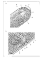
- FIG. 1 is a partially cutaway perspective sectional view showing a schematic configuration of a structure according to an embodiment (Embodiment 1) of the present invention, and (b) is the vicinity of a through hole and a protrusion provided in the structure.
- FIG. It is a side sectional view showing a schematic structure of a structure concerning one embodiment (embodiment 1) of the present invention. It is a figure which shows typically the outline
- (A) is side sectional drawing
- (b) is a perspective view. It is side sectional drawing which shows schematic structure of the structure which concerns on one Embodiment (Embodiment 2) of this invention.
- the structure according to the present invention is a structure formed by forming a second resin layer on a first resin layer having a conductive pattern formed on the surface thereof so as to sandwich the conductive pattern. Is provided with a first through-hole, and the conductive pattern passes through the first through-hole, and the second resin in the first resin layer from the first surface on the second resin layer side in the first resin layer. It extends to the second surface opposite to the layer, and the second resin layer has a first protrusion that fills at least a part of the first through hole.
- the wireless communication device is configured to include a housing including the structure according to the present invention and an antenna including the conductive pattern.
- the structure according to the present invention is incorporated in a general electronic device that requires a conductive pattern as an antenna element, a signal transmission path, a power transmission path, and the like, thereby providing the conductive pattern to the electronic device.
- a structure according to the present invention is incorporated in a wireless communication device and provides an antenna element of an antenna included in the wireless communication device.
- the structure according to the present invention may be incorporated in an electronic device, for example, to provide a signal transmission path, a power transmission path, and the like that connect a circuit board and other electronic components, or a circuit. A path for connecting the substrate and the ground may be provided.
- the structure according to the present invention may be fixed to the electronic device or may be detachably attached.
- the structure according to an embodiment of the present invention may constitute at least a part of a housing of the electronic device.
- the structure according to the present invention can constitute a conductive pattern forming housing.
- the casing refers to a member that stores an electronic component included in the electronic device
- the conductive pattern forming casing refers to a casing in which a conductive pattern is formed.
- the structure according to the present invention is not limited to this, and may be a member other than the casing included in the electronic device.
- the conductive pattern is sandwiched between the first resin layer and the second resin layer, exposure of the conductive pattern to the outside can be suppressed. Thereby, aesthetics can be secured and damage, deformation, deterioration, etc. of the conductive pattern can be prevented.
- Both the first resin layer and the second resin layer are injection molded products, and may be made of the same resin or different resins.
- the resin constituting the first resin layer and the second resin layer is not limited to these.
- acrylonitrile-butadiene-styrene resin ABS
- polycarbonate-acrylonitrile-butadiene-styrene resin PC-ABS
- One or more resins selected from polycarbonate (PC), acrylonitrile-styrene resin (AS), polyethylene (PE), polypropylene (PP), polystyrene (PS), methacrylic resin (PMMA) and the like can be used. These resins may be mixed with other materials such as glass in order to increase the strength.
- a resin having higher heat resistance than the resin constituting the second resin layer may be used as the resin constituting the first resin layer.
- a resin having higher heat resistance than the resin constituting the second resin layer may be used as the resin constituting the first resin layer.
- PC can be used as the resin constituting the first resin layer
- ABS can be used as the resin constituting the second resin layer.
- the conductive pattern is a pattern made of a conductor formed on the surface of the first resin layer.
- the kind of the conductor is not particularly limited as long as it has conductivity, and metals such as copper, iron, nickel, and gold, conductive polymers, conductive carbon, and the like can be used.
- the method for forming the conductive pattern is not particularly limited.
- the conductive pattern may be formed by plating a metal on the surface of the first resin layer, or a conductive paste containing a conductor
- a conductive pattern may be formed by printing on the surface of one resin layer, or a conductive pattern by sticking a flexible thin film conductive material such as copper foil to the surface of the first resin layer. May be formed.
- the conductor used for forming the conductive pattern is not limited to one type.
- a conductive pattern may be formed by combining a plurality of conductors such as gold plating on a copper pattern.
- the conductive pattern can be formed using an LDS (Laser Direct Structure) method. That is, an organic metal is mixed with the resin constituting the first resin layer, and the region on the surface of the first resin layer where the conductive pattern is formed is irradiated with laser. Thereby, an organic metal is deposited on the laser irradiation portion, and the laser irradiation portion is finely roughened (unevenness is formed), and the organic metal is bonded to the laser irradiation portion, thereby suitably forming a conductive pattern. be able to.
- the conductive pattern may be formed using a DPA (Direct Printed Antenna) method.
- the DPA method is a method in which a printing plate for preparing a conductive pattern is prepared in advance, and the shape of the conductive pattern is transferred from the plate to a resin surface with a pad or the like.
- the conductive pattern is generated on the surface of the first resin layer by laser irradiation, the first resin layer and the conductive pattern adhere very strongly.
- the structure according to the present invention can be manufactured, for example, as follows. First, using a known injection molding technique, a first resin layer having a penetrating through hole is formed into a desired shape (first resin layer forming step). Next, a conductive pattern is formed on the surface of the first resin layer using the method described above (conductive pattern forming step). Thereafter, a second resin layer is laminated on the first resin layer so as to sandwich the conductive pattern (lamination process). In the laminating step, it is preferable to insert-mold the second resin layer so as to be integrally molded with the already formed first resin layer.
- the second resin layer insert molding
- the first resin layer and the second resin layer are formed into the missing portion. It is possible to satisfactorily adhere (adhere) in a region where there is no conductive pattern containing.
- FIG. 1A is a partially cutaway perspective sectional view showing a schematic configuration of a structure 10 according to the present embodiment.
- the structure 10 includes a first resin layer 11, a second resin layer 21, a conductive pattern 31, and a conductive pattern 41.
- the conductive pattern 41 is provided between the first resin layer 11 and the second resin layer 21 and is electrically connected to the conductive pattern 31.
- a portion where the conductive pattern 41 is not formed is referred to as an interface 23 between the first resin layer 11 and the second resin layer 21.
- FIG. 1B is an enlarged view of the vicinity of the through hole 12 of the first resin layer 11 and the protrusion 22 of the second resin layer 21.
- the through hole 12 is a first through hole.
- a surface on the side in contact with the second resin layer 21 is defined as a first surface, and is a surface facing the first surface, which is an inner surface of the casing formed by the structure 10. Is defined as the second side.
- the through hole 12 is provided so as to penetrate the first surface and the second surface of the first resin layer 11. That is, the opening part of the through-hole 12 is formed in the 1st surface and the 2nd surface of the 1st resin layer 11, respectively.
- the conductive pattern 31 is formed on the through hole 12 and the outer edge of the opening of the through hole 12 formed in each of the first surface and the second surface of the first resin layer 11. Is provided.
- the conductive pattern 31 is formed along the shape of the through hole 12 and preferably penetrates in the same manner as the through hole 12.
- the conductive pattern 31 is configured to conduct the conductive pattern 51 provided on the second surface side of the first resin layer 11 and the conductive pattern 41 provided on the first surface side through the through hole 12. Can express.
- the conductive pattern 41 and the conductive pattern 51 are both formed in the same manufacturing process as the conductive pattern 31. That is, the conductive pattern 31, the conductive pattern 41, and the conductive pattern 51 are integrally formed. In this embodiment, since each member has a different function, the conductive pattern 31, the conductive pattern 41, and the conductive pattern 51 are divided into three parts, but the boundary of each member is not clearly defined. . Since each of the three members is electrically connected, the power supplied to the conductive pattern 51 is supplied to the conductive pattern 41.
- the second resin layer 21 is formed by laminating a resin on the first surface of the first resin layer 11 on which the conductive pattern 41 is provided. At this time, a part of the resin forming the second resin layer 21 is filled into the conductive pattern 31 formed along the shape of the through hole 12. That is, the second resin layer 21 includes a protrusion 22 having a shape that matches the through hole 12. The protrusion 22 is a first protrusion.
- the through-hole 12 is configured such that the area of the cross section perpendicular to the penetration direction becomes smaller as the distance from the second resin layer 21 increases in the penetration direction.
- the shape of the through hole 12 is a truncated cone whose tip is thinner than the root. Since the conductive pattern 31 is formed along the through-hole 12 having such a shape and the conductive pattern 31 penetrates, the resin that forms the through-hole 12 and the second resin layer 21 is the through-hole 12. Can be filled easily and uniformly.
- the shape of the through hole provided in the first resin layer is not limited to the above.
- vertical with respect to the penetration direction of a through-hole is not limited to circular, It can be made into arbitrary shapes.
- the angle formed by the through direction of the through hole 12 that is a truncated cone and the side surface of the through hole 12 is generally 10 degrees so that laser irradiation is easy. It is preferable that it is above, and it is more preferable that it is 30 degrees or more. According to the said structure, LDS method can be implemented successfully.
- the conductive pattern 31 integrally formed with the conductive pattern 41 is drawn from the first surface side of the first resin layer 11 to the second surface side.
- the conductive pattern 41 is brought into close contact with the first resin layer 11 and has an effect of being difficult to peel from the first resin layer 11.
- the second resin layer 21 is filled with at least a part of the through hole 12 by providing the second resin layer 21 with the protrusion 22 having a shape matching the through hole 12.
- the first resin layer 11 and the second resin layer 21 are in a state where they are tightly fitted.
- the first resin layer 11 and the second resin layer 21 are in close contact with each other, and the first resin layer and the second resin layer are unlikely to peel off at the portions where the conductive patterns 31 and 41 are provided.
- the structure 10 configured as described above is a portion in which the conductive pattern 41 is provided in the structure in which the conductive pattern 41 is provided between the first resin layer 11 and the second resin layer 21. The effect which suppresses peeling with the 1st resin layer 11 and the 2nd resin layer 21 in is produced.
- the first resin layer 11 and the second resin layer 21 can be prevented from being separated.
- the peeling between the conductive pattern 41 and the first resin layer 11 and the peeling between the first resin layer 11 and the second resin layer 21 have a great influence on the antenna characteristics.
- the designer designs the antenna on the assumption that the positional relationship between the antenna conductor circuit and the dielectric package material is constant.
- the antenna conductor circuit and the package material are separated, a gap is formed between the antenna conductor circuit and the package material, and the positional relationship between the antenna conductor circuit and the package material becomes unstable, resulting in variations in antenna characteristics. Since the structure 10 can suppress the peeling between the conductive pattern 41 and the first resin layer 11 and the peeling between the first resin layer 11 and the second resin layer 21, the above-described variation in antenna characteristics can be suppressed. it can.
- the structure 10 is configured to fix the conductive pattern 31 by sandwiching the through hole 12 and the protruding portion 22. Since this fixing is strong, the strength of the power supply spring for supplying power to the conductive pattern 51 can be set strongly. As a result, the adhesion between the second resin layer 21 and the conductive pattern 41 can be made uniform, and as a result, variations in the resonance frequency of the antenna characteristics in the conductive pattern 41 can be suppressed.
- the structure 10 does not require a reserved area as compared with the technique described in Patent Document 1. Therefore, the thickness of the structure can be further reduced. Furthermore, the reserved area is often made of a highly conductive resin and a metal material. There is a possibility that the surface resistance of the holding area configured as described above is increased. This is because, as described above, the material constituting the reserved area includes a material that is not a conductor. When the resistance value of the reserved area including the surface resistance is increased, the power efficiency when supplying power is deteriorated. Since the structure 10 connects the conductive pattern 51 and the conductive pattern 41 with the conductive pattern 31 made of a material having a low resistivity, it is possible to suppress deterioration in power efficiency caused by power supply.
- the structure 10 including the conductive pattern 31 that connects the conductive pattern 51 and the conductive pattern 41 that is a rectangle 40 mm long ⁇ 1 mm wide has a resistance value of about 1 ⁇ at the conductive pattern 51 and the tip of the conductive pattern 41. Can be suppressed.
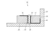
- FIG. 2 is a side sectional view showing a schematic configuration of a structure 10 ′ according to a modification of the present embodiment.
- the conductive pattern 31 and the conductive pattern 41 are not continuous. However, actually, the conductive pattern 31 and the conductive pattern 41 are integrally formed and continuous members.
- the conductive pattern 31 ′ and the conductive pattern 41 included in the structure 10 ′ are also integrally formed and continuous members. In order to clarify this, in FIG. 2, the conductive pattern 31 ′ and the conductive pattern 41 are illustrated so as to be continuous. The same applies to FIGS. 4 to 7 described later.
- a cylindrical through hole 12 ′ is provided in the first resin layer 11 ′.
- the shape of the through hole 12 ′ is a cylinder whose cross-sectional area perpendicular to the penetrating direction does not depend on the distance from the second resin layer 21 ′.
- a surface corresponding to the side surface of the cylinder is expressed as a side surface of the through hole 12 ′.
- the side surface of protrusion part 22 'corresponding to the side surface of through-hole 12' is formed so that it may become substantially perpendicular
- the side surfaces of the through hole 12 ′ and the protrusion 22 ′ do not have an inclination that makes it easy for the protrusion 22 ′ to come out of the conductive pattern 31 ′. Therefore, the structure 10 ′ more effectively suppresses the separation between the first resin layer 11 ′ and the second resin layer 21 ′ at the portion where the conductive pattern 41 is provided, compared to the structure 10. The effect to do.
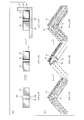
- FIG. 3 is a diagram schematically showing an outline of the manufacturing process of the structure 10 ′.
- 3A is a side cross-sectional view of a region near the through hole 12 in the structure 10 ′
- FIG. 3B is a region including the conductive pattern 41 and the conductive pattern 51 in the structure 10 ′.
- FIG. 3A is a side cross-sectional view of a region near the through hole 12 in the structure 10 ′
- FIG. 3B is a region including the conductive pattern 41 and the conductive pattern 51 in the structure 10 ′.
- a first resin layer 11 ' having a through-hole 12' passing therethrough is formed.
- the first resin layer has two through holes.
- the manufacturing process will be described taking the through hole 12 'as an example.
- openings 12a ′ and formed on the first surface This is referred to as an opening 12b ′.
- the conductive pattern 31 ', the conductive pattern 41, and the conductive pattern 51 are formed on the first resin layer 11' by using, for example, plating. More specifically, the conductive pattern 51 is formed on the second surface of the first resin layer 11 ′, the conductive pattern 41 is formed on the first surface, and the conductive pattern 31 ′ is the side surface of the through-hole 12 ′ and the opening 12a. The outer edge of 'and the outer edge of the opening 12b' are formed.
- the second resin layer 21 ' is formed so as to sandwich the conductive pattern 41 together with the first resin layer 11'.
- the resin that forms the second resin layer 21 ′ is injected into the mold, the resin is also filled into the penetrating portion of the conductive pattern 31 ′ that passes therethrough. At this time, a gas such as air existing in the vicinity of the conductive pattern 31 ′ is discharged through the through portion of the conductive pattern 31 ′. Therefore, the resin forming the second resin layer 21 ′ is easily and uniformly filled in the through portions of the conductive pattern 31.
- the upper end of the conductive pattern 31 ′ is closed if the resin can be filled without leaving a gas such as air inside the conductive pattern 31 ′. May be.
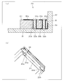
- FIG. 4 is a side sectional view showing a schematic configuration of the structure 110 according to the present embodiment.
- symbol is attached and the description is abbreviate
- the structure 110 differs in the shape of the through-hole 112 provided in the 1st resin layer 111 compared with the structure 10 and structure 10 'which concern on Embodiment 1.
- the through hole 112 is configured such that an area of a cross section perpendicular to the penetrating direction increases as the distance from the second resin layer 121 increases in the penetrating direction.
- the through hole 112 and the tip of the protrusion are configured to be thicker than the root of the through hole 112. Therefore, the through hole 112 and the protrusion 122 in the structure 110 are configured such that the protrusion 122 does not come off from the conductive portion 131.
- the structural body 110 has the protrusions 122 provided in the second resin layer 121 further removed from the through holes 112 and the conductive portions 131. It is configured so that it is difficult and firmly fixed. According to this configuration, the strength of the power supply spring for supplying power to the conductive pattern 51 can be set more strongly. That is, the adhesion between the second resin layer 121 and the conductive pattern 41 can be made more uniform, and as a result, variations in the resonance frequency of the antenna characteristics in the conductive pattern 41 can be further suppressed.
- FIG. 5 is a diagram illustrating a schematic configuration of the structure 210 according to the present embodiment.
- (A) of FIG. 5 is a figure which shows a mode that each member with which the structure 210 is provided on the side cross section is projected,
- (b) of FIG. 5 is a perspective view.
- the structure 210 includes a first resin layer 211 provided with a first through hole 212a and a second through hole 212b, and a second resin layer 221 provided with a first protrusion 222a and a second protrusion 222b. It has. Conductive patterns 231a are provided on the outer edges of the first through holes 212a and the first through holes 212a, and conductive patterns 231b are provided on the outer edges of the second through holes 212b and the second through holes 212b. It has been.
- the first protrusion 222a is a protrusion having a shape matching the first through hole 212a
- the second protrusion 222b is a protrusion having a shape matching the second through hole 212b.
- the conductive pattern 241 provided between the first resin layer 211 and the second resin layer 221 electrically connects the conductive pattern 231a and the conductive pattern 231b and is conductive.
- a conductive pattern 251a that is conductive with the conductive pattern 231a and a conductive pattern 251b that is conductive with the conductive pattern 231b are formed.
- the structure 210 is different in that both ends of the conductive pattern 241 are fixed to the first resin layer 211 and the second resin layer 221.
- One end of the conductive pattern 241 is connected to the conductive pattern 231a, and the other end is connected to the conductive pattern 231b.
- the conductive pattern 231a is firmly fixed to the first resin layer 211 and the second resin layer 221 by being sandwiched between the first through hole 212a and the first protrusion 222a.
- the conductive pattern 231b is also firmly fixed to the first resin layer 211 and the second resin layer 221.
- both ends of the conductive pattern 241 included in the structure 210 are firmly fixed to the first resin layer 211 and the second resin layer 221.
- the conductive pattern 241 is used as an antenna, it is possible to firmly fix not only the power feeding unit that supplies power but also the tip of the antenna, so that the adhesion between the conductive pattern 241 and the second resin layer 221 is further improved. It is possible to make it uniform.
- the tip of the antenna is often disposed in the outer edge region of the structure 210.
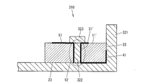
- FIG. 6 is a side sectional view showing a schematic configuration of the structure 310 according to the present embodiment.
- the structure 310 has a configuration similar to the structure 10 ′ according to the modification of the first embodiment.
- the structure 310 includes a plug-shaped portion 323 that is in close contact with the outer edge of the opening of the through hole 12 ′ via at least the conductive pattern 31 ′ and is provided so as to close the through hole 12 ′.
- the outer edge of the opening refers to the outer edge of the opening formed on the second surface of the first resin layer 11 ′.
- the plug-shaped portion 323 can be formed, for example, by causing the resin to overflow from the penetrating portion penetrating the conductive pattern 31 ′ in the step of forming the second resin layer 321.
- the shape of the plug-shaped portion 323 is not limited, and may be configured so as to at least close the through hole 12 ′.
- the conductive pattern 31 ′ of the structure 310 is more firmly fixed to the first resin layer 11 ′ and the second resin layer 321 by the plug-shaped portion 323.
- the plug-shaped portion 323 prevents the adhesiveness between the conductive pattern 31 ′ and the first resin layer 11 ′ and the protrusion 322 from being lowered, and the mutual fixation is prevented from being relaxed.
- the conductive pattern 41 is used as an antenna, it is possible to more firmly fix the power supply unit that supplies power, so that the adhesion between the conductive pattern 41 and the second resin layer 221 can be made more uniform. is there. Therefore, variation in the resonance frequency of the antenna characteristics in the conductive pattern 41 can be further suppressed, and the antenna characteristics of the conductive pattern 41 can be further stabilized.
- the plug-shaped portion 323 may be formed in a region wider than a region where the conductive pattern 31 'is formed. According to this configuration, the plug-shaped portion 323 made of resin and the first resin layer 11 ′ are in direct contact without interposing the conductive pattern 31 ′. Therefore, according to the configuration, the effect produced by the structure 310 can be further enhanced.
- FIG. 7 is a schematic diagram schematically showing the configuration of the wireless communication device 1.
- the wireless communication device 1 has a structure 10 ′ and an internal device 5, and the structure (lower housing) 10 ′ together with the upper housing 7 constitutes a housing of the wireless communication device 1.
- the internal device 5 includes an electronic circuit unit 2, an internal substrate 3, and a mounting component 4.
- the internal substrate 3 is a substrate for mounting the mounting component 4 and the electronic circuit unit 2 for realizing various functions of the wireless communication device 1.
- the electronic circuit unit 2 is connected to the conductive pattern 41 via the power supply spring 6, the conductive pattern 51, and the like.
- the conductive pattern 31 ′ is firmly fixed to the first resin layer 11 ′ and the second resin layer 21 ′. Therefore, the power supply spring 6 that supplies power to the conductive pattern 41 can be configured to be more firmly fixed to the conductive pattern 51. That is, the adhesion between the conductive pattern 41 and the second resin layer 21 ′ can be made more uniform. Therefore, variation in the resonance frequency of the antenna characteristics in the conductive pattern 41 can be further suppressed, and the antenna characteristics of the conductive pattern 41 can be further stabilized.
- the conductive pattern 51 is a connection portion for connecting the conductive pattern 41 to the internal substrate 3. Variations in adhesion between the conductive pattern 51 and the first resin layer 11 ′, which are connection parts, cause variations in antenna performance.
- the antenna is preferably arranged as far as possible from the internal device 5.
- the conductive pattern 41 can be disposed on the outer side.
- the conductive pattern 51 is often designed as a circle having a diameter of about 2 mm with the contact point with the power supply spring 6 as the center. Therefore, in the wireless communication device 1, the conductive pattern 31 ′ can be disposed at a distance of about 1-3 mm from the contact center of the power supply spring 6.
- the structure (10) according to the first aspect of the present invention has a second resin layer (21) that sandwiches the conductive pattern on the first resin layer (11) having the conductive pattern (41) formed on the surface thereof.
- the first resin layer (11) has a first through hole (12)
- the conductive pattern (31, 41, 51) has a first through hole ( 12), extending from the first surface of the first resin layer on the second resin layer side to the second surface of the first resin layer opposite to the second resin layer, (21) includes a first protrusion (22) that fills at least a portion of the first through hole (12).
- At least one part of the through-hole provided in the 1st resin layer is by the protrusion part of the 2nd resin layer shape
- the first resin layer and the second resin layer are in close contact with each other. Therefore, there exists an effect which suppresses peeling with a 1st resin layer and a 2nd resin layer in the part in which the conductive pattern is provided.
- the tip of the first protrusion (122) is thicker than the root of the first protrusion.
- the first protrusion is configured to be more firmly fixed from the first through hole and the conductive pattern.
- the strength of the power supply spring can be set more strongly. Therefore, variation in the resonance frequency of the antenna characteristics in the conductive pattern can be further suppressed.
- the first resin layer (211) is further provided with a second through hole (212b), and the conductive pattern (241). Is extended from the first surface to the second surface through the first through hole (212a) on one end side, and the first through the second through hole (212b) on the other end side.
- the second resin layer (221) may further include a second protrusion (222b) that fills at least part of the second through hole (212b).
- both ends of the conductive pattern included in the structure are firmly fixed to the first resin layer and the second resin layer. Therefore, the antenna characteristics of the conductive pattern can be further stabilized.
- the structure according to Aspect 4 of the present invention is the plug according to any one of Aspects 1 to 3, wherein the first protrusion (322) is provided on the second surface so as to close the through hole.
- a portion (323) may be provided.
- the conductive pattern 31 ′ is more firmly fixed to the first resin layer 11 ′ and the second resin layer 321 by the plug-shaped portion 323.
- the plug-shaped portion 323 prevents the adhesion between the conductive pattern 31 ′ and the first resin layer 11 ′ and the protrusion 322 from being lowered. Therefore, the antenna characteristics of the conductive pattern can be further stabilized.
- a wireless communication device (1) according to aspect 5 of the present invention includes a housing including the structure according to any one of aspects 1 to 4, and an antenna including the conductive pattern. It is preferable.
- the present invention can be widely applied to various electronic components using a conductive pattern. Although not particularly limited to this, the present invention can be suitably applied to a wireless communication apparatus that uses a conductive pattern as an antenna element.
Landscapes
- Engineering & Computer Science (AREA)
- Microelectronics & Electronic Packaging (AREA)
- Computer Networks & Wireless Communication (AREA)
- Details Of Aerials (AREA)
- Support Of Aerials (AREA)
Abstract
第一樹脂層(11)には第一貫通孔(12)が設けられており、導電パターン(31、41、51)は、第一貫通孔(12)を通って、第一樹脂層(11)の第一面から、第一樹脂層(11)の第二面まで延在しており、第二樹脂層(21)は、第一貫通孔(12)の少なくとも一部を充填する第一突起部(22)を備えている。
Description
本発明は、導電パターンを備える構造体、および当該構造体を備える無線通信装置に関する。
近年、電子装置の薄型化、およびその構成の簡素化のために、導電パターンを筺体と一体的に形成する技術が開発されている。例えば、特許文献1には、アンテナ導体回路を備えている無線通信製品のケーシングが記載されている。ケーシングは、アンテナ導体回路と形状が相合わせられ導電性を有する保留エリアを備えている。アンテナ導体回路は、保留エリアにメッキまたは電気鋳造方式によって形成された後に、パッケージ材によって覆われる。
上述の技術において、ケーシングおよびパッケージ材の界面は、互いに溶け合うことによって密着可能である。一方、アンテナ導体回路およびパッケージ材の界面は、互いに溶け合いにくく密着することが難しい。この密着の難しさは、アンテナ導体回路がメッキによって覆われており、このメッキからなる部分が溶けないことに起因する。したがって、アンテナ導体回路およびパッケージ材は、その界面において剥離する虞がある。
本発明は、上記の課題に鑑みてなされたものであり、その主たる目的は、第一樹脂層および第二樹脂層の層間に導電パターンが設けられている構造体において、導電パターンが設けられている部分での第一樹脂層と第二樹脂層との剥離を抑制するための技術を提供することを主たる目的とする。
上記の課題を解決するために、本発明の一態様に係る構造体は、その表面に導電パターンが形成された第一樹脂層上に、当該導電パターンを挟むように第二樹脂層を成形してなる構造体であって、第一樹脂層には、第一貫通孔が設けられており、上記導電パターンは、第一貫通孔を通って、第一樹脂層における第二樹脂層側の第一面から、第一樹脂層における第二樹脂層とは反対側の第二面まで延在しており、第二樹脂層は、第一貫通孔の少なくとも一部を充填する第一突起部を備えている。
本発明の一態様によれば、第一樹脂層に設けられている第一貫通孔の少なくとも一部が、第一樹脂層上に成形される第二樹脂層の第一突起部によって充填され、あたかも強嵌合しているような状態となる。これによって、第一樹脂層と第二樹脂層とが強く密着し、導電パターンが設けられている部分において第一樹脂層と第二樹脂層との剥離を抑制する効果を奏する。
本発明に係る構造体は、その表面に導電パターンが形成された第一樹脂層上に、当該導電パターンを挟むように第二樹脂層を成形してなる構造体であって、第一樹脂層には、第一貫通孔が設けられており、上記導電パターンは、第一貫通孔を通って、第一樹脂層における第二樹脂層側の第一面から、第一樹脂層における第二樹脂層とは反対側の第二面まで延在しており、第二樹脂層は、第一貫通孔の少なくとも一部を充填する第一突起部を備えている構成である。
また、本発明に係る無線通信装置は、本発明に係る構造体を含んでなる筐体と、上記導電パターンを含んでなるアンテナと、を備えている構成である。
(構造体の概要)
本発明に係る構造体は、アンテナエレメント、信号伝送経路、電力伝送経路等としての導電パターンを必要とする電子装置一般に組み込まれることで、当該電子装置に当該導電パターンを提供するものである。例えば、一実施形態において、本発明に係る構造体は、無線通信装置に組み込まれ、当該無線通信装置が備えるアンテナのアンテナエレメントを提供するようになっている。本発明に係る構造体は、また、例えば、電子装置に組み込まれ、回路基板と他の電子部品とを接続する信号伝送経路、電力伝送経路等を提供するようになっていてもよいし、回路基板とグランドとを接続する経路を提供するようになっていてもよい。
本発明に係る構造体は、アンテナエレメント、信号伝送経路、電力伝送経路等としての導電パターンを必要とする電子装置一般に組み込まれることで、当該電子装置に当該導電パターンを提供するものである。例えば、一実施形態において、本発明に係る構造体は、無線通信装置に組み込まれ、当該無線通信装置が備えるアンテナのアンテナエレメントを提供するようになっている。本発明に係る構造体は、また、例えば、電子装置に組み込まれ、回路基板と他の電子部品とを接続する信号伝送経路、電力伝送経路等を提供するようになっていてもよいし、回路基板とグランドとを接続する経路を提供するようになっていてもよい。
なお、本発明に係る構造体は、電子装置に固定されていてもよいし、着脱可能に装着されていてもよい。本発明の一実施形態に係る構造体は、電子装置の筐体の少なくとも一部を構成してもよい。言い換えれば、本発明に係る構造体は、導電パターン形成筐体を構成し得る。なお、筐体とは、電子装置が備える電子部品を格納する部材を指し、導電パターン形成筐体とは、導電パターンが形成されている筐体を指す。但し、本発明に係る構造体は、これに限定されず、電子装置が備える筐体以外の部材であってもよい。
本発明に係る構造体では、導電パターンが第一樹脂層および第二樹脂層によって挟まれているために、導電パターンの外部への露出を抑制することができる。これにより、美観を確保し、導電パターンの損傷、変形、劣化等を防ぐことができる。
第一樹脂層および第二樹脂層は、ともに射出成形物であり、同じ樹脂から構成されていても、異なる樹脂から構成されていてもよい。第一樹脂層および第二樹脂層を構成する樹脂としては、これらに限定するものではないが、例えば、アクリロニトリル-ブタジエン-スチレン樹脂(ABS)、ポリカーボネート-アクリロニトリル-ブタジエン-スチレン樹脂(PC-ABS)、ポリカーボネート(PC)、アクリロニトリル-スチレン樹脂(AS)、ポリエチレン(PE)、ポリプロピレン(PP)、ポリスチレン(PS)、メタクリル樹脂(PMMA)等から選択される一種類以上の樹脂を用いることができる。また、これらの樹脂には、強度を上げるためにガラス等の他の材料を混合してもよい。
また、一つの局面において、第一樹脂層を構成する樹脂として、第二樹脂層を構成する樹脂よりも耐熱性を有する樹脂を用いてもよい。これにより、第二樹脂層を成形するときに、第一樹脂層および第二樹脂層を形成する樹脂が過度に溶け合うことを抑制できる。例えば、第一樹脂層を構成する樹脂としてPC、第二樹脂層を構成する樹脂としてABSを用いることができる。
導電パターンは、第一樹脂層の表面に形成された導電体からなるパターンである。導電体の種類は、導電性を有するものであれば特に限定されず、銅、鉄、ニッケル、金等の金属、導電性ポリマー、導電性カーボン等を用いることができる。また、導電パターンの形成方法は、特に限定されないが、例えば、金属を、第一樹脂層の表面にメッキすることによって導電パターンを形成してもよいし、導電体を含有する導電ペーストを、第一樹脂層の表面に印刷することによって導電パターンを形成してもよいし、銅箔などの可撓性を有する薄膜状の導電性体を、第一樹脂層の表面に貼付することによって導電パターンを形成してもよい。また、導電パターンの形成に用いる導電体は一種類に限定されない。例えば、銅パターンの上に金メッキを施すなど、複数の導電体を組み合わせて導電パターンを形成してもよい。
例えば、一実施形態において、LDS(Laser Direct Structuring)法を用いて導電パターンを形成することができる。すなわち、第一樹脂層を構成する樹脂に有機金属を混合しておき、第一樹脂層の表面の導電パターンを形成する領域にレーザ照射する。これによって、レーザ照射部へ有機金属を析出させ、また、レーザ照射部を微細に荒らして(凹凸を作り)、当該有機金属をそのレーザ照射部に結合させることにより、導電パターンを好適に形成することができる。また、他の実施形態において、DPA(Direct Printed Antenna)法を用いて導電パターンを形成してもよい。DPA法とは、あらかじめ導電パターンを作成するための印刷版を用意し、その版から導電パターン形状をパットなどにより樹脂面へ転写する方法である。
上述の方法、特にLDS法では、レーザ照射により第一樹脂層の表面に導電パターンを生成しているため、第一樹脂層と導電パターンとが非常に強く密着する。
また、本発明に係る構造体は、例えば、以下のようにして製造することができる。まず、公知の射出成形技術を用いて、貫通している貫通孔を備える第一樹脂層を所望の形状に形成する(第一樹脂層形成工程)。次いで、上述した手法を用いて、第一樹脂層の表面に導電パターンを形成する(導電パターン形成工程)。その後、第一樹脂層上に、導電パターンを挟むように第二樹脂層を積層する(積層工程)。積層工程では、既に形成した第一樹脂層と一体に成形されるように第二樹脂層にインサート成型することが好ましい。すなわち、成形型に導電パターンを備えている第一樹脂層を配置した状態で、第二樹脂層を成形することにより(インサート成型)、第一樹脂層と第二樹脂層とを、上記欠落部位を含む導電パターンが存在していない領域において良好に密着(接着)することができる。
〔実施形態1〕
図1の(a)は、本実施形態に係る構造体10の概略構成を示す一部切欠き斜視断面図である。図1の(a)に示すように、構造体10は、第一樹脂層11、第二樹脂層21、導電パターン31および導電パターン41を備えている。導電パターン41は、第一樹脂層11および第二樹脂層21の層間に設けられており、導電パターン31と導通している。第一樹脂層11および第二樹脂層21の境界部分のうち、導電パターン41が形成されていない部分を、第一樹脂層11および第二樹脂層21の界面23と記載する。
図1の(a)は、本実施形態に係る構造体10の概略構成を示す一部切欠き斜視断面図である。図1の(a)に示すように、構造体10は、第一樹脂層11、第二樹脂層21、導電パターン31および導電パターン41を備えている。導電パターン41は、第一樹脂層11および第二樹脂層21の層間に設けられており、導電パターン31と導通している。第一樹脂層11および第二樹脂層21の境界部分のうち、導電パターン41が形成されていない部分を、第一樹脂層11および第二樹脂層21の界面23と記載する。
図1の(b)は、第一樹脂層11の貫通孔12および第二樹脂層21の突起部22の近傍を拡大した図である。貫通孔12は、第一貫通孔である。第一樹脂層11において、第二樹脂層21と接触する側の面を第一面と定義し、第一面に対向する面であって、構造体10が構成する筐体の内側となる面を第二面と定義する。貫通孔12は、第一樹脂層11の第一面と第二面とを貫通するように設けられている。すなわち、第一樹脂層11の第一面および第二面には、貫通孔12の開口部がそれぞれ形成されている。
図1の(b)に示すように、導電パターン31は、貫通孔12と、第一樹脂層11の第一表面および第二表面のそれぞれに形成されている貫通孔12の開口部外縁とに設けられている。導電パターン31は、貫通孔12の形状に沿って形成されており、貫通孔12と同様に貫通していることが好ましい。導電パターン31は、貫通孔12を介して、第一樹脂層11の第二面側に設けられている導電パターン51と、第一面側に設けられている導電パターン41とを導通させるものとも表現できる。
導電パターン41および導電パターン51は、いずれも導電パターン31と同じ製造工程において形成されるものである。すなわち、導電パターン31、導電パターン41および導電パターン51は、一体に形成されているものである。本実施形態では、各部材が異なる機能を備えるため導電パターン31、導電パターン41および導電パターン51の3つに分割して表現しているが、各部材の境界は明確に定義されるものではない。上記3つの各部材は電気的に導通しているため、導電パターン51に供給された電力は、導電パターン41に供給される。
第二樹脂層21は、導電パターン41が設けられている第一樹脂層11の第一面に樹脂を積層することによって形成される。この際、第二樹脂層21を形成する樹脂の一部は、貫通孔12の形状に沿って形成されている導電パターン31の内部へ充填される。すなわち、第二樹脂層21は、貫通孔12に合致する形状の突起部22を備えている。突起部22は、第一突起部である。
本実施形態において、貫通孔12は、その貫通方向に対して垂直な断面の面積が、貫通方向において第二樹脂層21から離れるほど小さくなるように構成されている。言い換えれば、貫通孔12の形状は、その先端が根本よりも細い円錐台である。このような形状の貫通孔12に沿って導電パターン31は形成されており、かつ、導電パターン31は貫通しているため、貫通孔12および第二樹脂層21を形成する樹脂は、貫通孔12の全体に容易かつ均一に充填される。なお、構造体10において、第一樹脂層に設けられている貫通孔の形状は、上記のものに限定されるものではない。また、貫通孔の貫通方向に対して垂直な断面の形状は、円形に限定されるものではなく任意の形状とすることができる。また、LDS法を用いて導電パターン31を形成する場合には、円錐台である貫通孔12の貫通方向と、貫通孔12の側面とのなす角は、一般にレーザ照射がしやすいように10度以上であることが好ましく、30度以上であることがより好ましい。当該構成によれば、首尾よくLDS法を実施することができる。
(実施形態1の利点)
構造体10において、導電パターン41と一体成形されている導電パターン31は、第一樹脂層11の第一面側から第二面側へ引き込まれている。このように導電パターン31および導電パターン41が形成されていることによって、導電パターン41は第一樹脂層11に密着し、第一樹脂層11から剥離しにくくなる効果を奏する。
構造体10において、導電パターン41と一体成形されている導電パターン31は、第一樹脂層11の第一面側から第二面側へ引き込まれている。このように導電パターン31および導電パターン41が形成されていることによって、導電パターン41は第一樹脂層11に密着し、第一樹脂層11から剥離しにくくなる効果を奏する。
そして、貫通孔12に合致する形状の突起部22が第二樹脂層21に設けられていることによって、第二樹脂層21は、貫通孔12の少なくとも一部を充填している。この構成によれば、第一樹脂層11と第二樹脂層21とが、あたかも強嵌合しているような状態となる。これによって、第一樹脂層11と第二樹脂層21とが強く密着し、導電パターン31および41が設けられている部分において第一樹脂層と第二樹脂層との剥離が起こり難くなる。
以上のように、導電パターン31を介しているものの、第一樹脂層11の貫通孔12と、第二樹脂層21の突起部22とは、形状が合致しているために良好に密着することができる。したがって、上述のように構成されている構造体10は、第一樹脂層11および第二樹脂層21の層間に導電パターン41が設けられている構造体において、導電パターン41が設けられている部分での第一樹脂層11と第二樹脂層21との剥離を抑制する効果を奏する。
また、例え導電パターン41が第二樹脂層21の広範囲に渡って形成されていても、第一樹脂層11と第二樹脂層21とが分離しないようにすることができる。
導電パターン41と第一樹脂層11との剥離、および、第一樹脂層11と第二樹脂層21との剥離は、アンテナ特性に対して大きな影響を与える。一般的に、アンテナ近くに誘電体を配置すると、その誘電体の誘電率および誘電正接によってアンテナの共振周波数がズレたり、性能としてロスすることが知られている。したがって、設計者は、アンテナ導体回路と誘電体からなるパッケージ材との位置関係が一定であることを前提にしてアンテナを設計する。アンテナ導体回路とパッケージ材とが剥離すると、アンテナ導体回路とパッケージ材との間に空隙が形成され、アンテナ導体回路とパッケージ材との位置関係が不安定になるため、アンテナ特性にばらつきが生じる。構造体10は、導電パターン41と第一樹脂層11との剥離、および、第一樹脂層11と第二樹脂層21との剥離を抑制可能なので、上述のアンテナ特性のばらつきを抑制することができる。
また、構造体10は、導電パターン31を、貫通孔12と突起部22とが挟むことによって固定する構成である。この固定は強固であるため、導電パターン51に電力を供給するための給電バネの強さを強く設定することができる。
このことにより、第二樹脂層21と導電パターン41との密着性を均一にすることが可能であり、ひいては、導電パターン41におけるアンテナ特性の共振周波数のばらつきを抑制することができる。
このことにより、第二樹脂層21と導電パターン41との密着性を均一にすることが可能であり、ひいては、導電パターン41におけるアンテナ特性の共振周波数のばらつきを抑制することができる。
また、構造体10は、特許文献1に記載されている技術と比較して、保留エリアを必要としない。したがって、構造体の厚みを、より薄型化することが可能である。さらに、保留エリアは、高導電性樹脂および金属材料からなる場合が多い。このように構成された保留エリアの表面抵抗は高くなる虞がある。これは、上述の通り、保留エリアの構成材料には導体でない材料も含まれているためである。表面抵抗を含めて保留エリアの抵抗値が高くなると、電力を給電する際の電力効率が悪化する。構造体10は、抵抗率の低い材料からなる導電パターン31によって導電パターン51と導電パターン41とを接続しているため、電力の給電に伴う電力効率の悪化を抑制可能である。たとえば、導電パターン51と、長さ40mm×幅1mmの長方形である導電パターン41とを接続する導電パターン31を備える構造体10は、導電パターン51と導電パターン41の先端とにおける抵抗値を1Ω程度に抑制することができる。
(変形例)
構造体10の変形例である構造体10’について、図2を参照しながら説明する。図2は、本実施形態の変形例に係る構造体10’の概略構成を示す側方断面図である。構造体10の導電パターン31を通る断面(図1の(a)参照)において、導電パターン31と導電パターン41とは連続していない。しかし、実際には、導電パターン31および導電パターン41は、一体形成され連続している部材である。構造体10’が備えている導電パターン31’および導電パターン41も、一体形成され連続している部材である。このことを明示するために、図2では、導電パターン31’と導電パターン41とが連続するように図示している。この点に関しては、後述する図4~7についても同様である。
構造体10の変形例である構造体10’について、図2を参照しながら説明する。図2は、本実施形態の変形例に係る構造体10’の概略構成を示す側方断面図である。構造体10の導電パターン31を通る断面(図1の(a)参照)において、導電パターン31と導電パターン41とは連続していない。しかし、実際には、導電パターン31および導電パターン41は、一体形成され連続している部材である。構造体10’が備えている導電パターン31’および導電パターン41も、一体形成され連続している部材である。このことを明示するために、図2では、導電パターン31’と導電パターン41とが連続するように図示している。この点に関しては、後述する図4~7についても同様である。
変形例に係る構造体10’において、筒状の貫通孔12’が第一樹脂層11’に設けられている。言い換えれば、貫通孔12’の形状は、その貫通方向に対して垂直な断面の面積が、第二樹脂層21’からの距離に依存しない円筒である。以下において、円筒の側面に相当する面を、貫通孔12’の側面と表現する。
上記の構成によれば、貫通孔12’の側面に対応する突起部22’の側面は、第一樹脂層11’の第一面および第二面に対して略垂直になるように形成されている。すなわち、貫通孔12’および突起部22’の側面は、突起部22’が導電パターン31’から抜けやすくなるような傾斜を有していない。したがって、構造体10’は、構造体10と比較して、導電パターン41が設けられている部分での第一樹脂層11’と第二樹脂層21’との剥離を、より効果的に抑制する効果を奏する。
(製造方法)
構造体10’の製造方法について、図3を参照しながら説明する。図3は、構造体10’の製造工程の概要を模式的に表す図である。図3の(a)は、構造体10’における貫通孔12の近傍領域の側方断面図であり、図3の(b)は、構造体10’における導電パターン41および導電パターン51を含む領域の斜視図である。
構造体10’の製造方法について、図3を参照しながら説明する。図3は、構造体10’の製造工程の概要を模式的に表す図である。図3の(a)は、構造体10’における貫通孔12の近傍領域の側方断面図であり、図3の(b)は、構造体10’における導電パターン41および導電パターン51を含む領域の斜視図である。
製造のステップ1では、貫通している貫通孔12’を備えている第一樹脂層11’が形成される。図3の(b)において、第一樹脂層は2つの貫通孔を備えているが、ここでは貫通孔12’を例に製造工程を説明する。なお、貫通孔12’が第一樹脂層11’に形成する開口部のうち、第一樹脂層11’の第二面に形成されるものを開口部12a’と記載し、第一面に形成されるものを開口部12b’と記載する。
製造のステップ2では、たとえばメッキを用いて導電パターン31’、導電パターン41および導電パターン51が、第一樹脂層11’に形成される。より具体的には、導電パターン51は第一樹脂層11’の第二面に形成され、導電パターン41は第一面に形成され、導電パターン31’は貫通孔12’の側面ならびに開口部12a’の外縁および開口部12b’の外縁に形成される。
製造のステップ3では、導電パターン41を、第一樹脂層11’とともに挟むように第二樹脂層21’が形成される。第二樹脂層21’を形成する樹脂が成形型に射出されると、当該樹脂は、貫通している導電パターン31’の貫通部にも充填される。この際、導電パターン31’の近傍に存在している空気などのガスは、導電パターン31’の貫通部を介して排出される。したがって、第二樹脂層21’を形成する樹脂は、導電パターン31の貫通部に容易に、かつ、均一に充填される。第二樹脂層21’を形成する際に、導電パターン31’の内部に空気などのガスが残留することなく樹脂を充填可能であるならば、導電パターン31’の上端は閉じているように構成されていてもよい。
〔実施形態2〕
図4は、本実施形態に係る構造体110の概略構成を示す側方断面図である。なお、以下の各実施形態の説明において、上記実施形態にて説明した部材と同じ機能を有する部材については、同じ符号を付記し、その説明を省略する。
図4は、本実施形態に係る構造体110の概略構成を示す側方断面図である。なお、以下の各実施形態の説明において、上記実施形態にて説明した部材と同じ機能を有する部材については、同じ符号を付記し、その説明を省略する。
構造体110は、実施形態1に係る構造体10および構造体10’と比較して、第一樹脂層111に設けられている貫通孔112の形状が異なる。より具体的には、貫通孔112は、その貫通方向に対して垂直な断面の面積が、貫通方向において第二樹脂層121から離れるほど大きくなるように構成されている。言い換えれば、貫通孔112および突起部の先端は、貫通孔112の根本よりも太いように構成されている。したがって、構造体110における貫通孔112および突起部122は、突起部122が導電部131から抜けないように構成されている。
(実施形態2の利点)
実施形態1に係る構造体10および構造体10’と比較して、構造体110は、第二樹脂層121に設けられている突起部122が、貫通孔112および導電部131から、より一層抜けにくく強固に固定されるように構成されている。この構成によれば、導電パターン51に電力を供給するための給電バネの強さをより強く設定することができる。すなわち、第二樹脂層121と導電パターン41との密着性をより均一にすることが可能であり、ひいては、導電パターン41におけるアンテナ特性の共振周波数のばらつきをより抑制することができる。
実施形態1に係る構造体10および構造体10’と比較して、構造体110は、第二樹脂層121に設けられている突起部122が、貫通孔112および導電部131から、より一層抜けにくく強固に固定されるように構成されている。この構成によれば、導電パターン51に電力を供給するための給電バネの強さをより強く設定することができる。すなわち、第二樹脂層121と導電パターン41との密着性をより均一にすることが可能であり、ひいては、導電パターン41におけるアンテナ特性の共振周波数のばらつきをより抑制することができる。
〔実施形態3〕
図5は、本実施形態に係る構造体210の概略構成を示す図である。図5の(a)は、側方断面に構造体210が備えている各部材を投影した様子を示す図であり、図5の(b)は、斜視図である。
図5は、本実施形態に係る構造体210の概略構成を示す図である。図5の(a)は、側方断面に構造体210が備えている各部材を投影した様子を示す図であり、図5の(b)は、斜視図である。
構造体210は、第一貫通孔212aおよび第二貫通孔212bが設けられている第一樹脂層211と、第一突起部222aおよび第二突起部222bが設けられている第二樹脂層221とを備えている。第一貫通孔212aおよび第一貫通孔212aの開口部外縁には、導電パターン231aが設けられており、第二貫通孔212bおよび第二貫通孔212bの開口部外縁には、導電パターン231bが設けられている。第一突起部222aは、第一貫通孔212aに合致する形状の突起部であり、第二突起部222bは、第二貫通孔212bに合致する形状の突起部である。さらに、第一樹脂層211および第二樹脂層221の層間に設けられている導電パターン241は、導電パターン231aと導電パターン231bとを電気的に接続し導通している。また、第一樹脂層211の第二面には、導電パターン231aと導通する導電パターン251a、および、導電パターン231bと導通する導電パターン251bが形成されている。
上述の各実施形態に係る構造体と比較して、構造体210は、導電パターン241の両端が、第一樹脂層211および第二樹脂層221に固定されている点が異なる。導電パターン241の一端は導電パターン231aに接続されており、他方の一端は導電パターン231bに接続されている。導電パターン231aは、第一貫通孔212aおよび第一突起部222aに挟まれることによって、第一樹脂層211および第二樹脂層221に対して強固に固定されている。同様に、導電パターン231bも、第一樹脂層211および第二樹脂層221に対して強固に固定されている。
(実施形態3の利点)
上述のように、構造体210が備えている導電パターン241は、その両端が第一樹脂層211および第二樹脂層221に対して強固に固定されている。導電パターン241をアンテナとして使用する場合、電力を供給する給電部のみならずアンテナの先端部をも強固に固定することが可能なため、導電パターン241と第二樹脂層221との密着性をより均一にすることが可能である。また、通常、アンテナの先端は、構造体210の外縁領域に配置されることが多い。そのアンテナの先端部を強固に固定することによって、導電パターン241におけるアンテナ特性の共振周波数のばらつきをより抑制することができ、導電パターン241のアンテナ特性をより安定化することができる。
上述のように、構造体210が備えている導電パターン241は、その両端が第一樹脂層211および第二樹脂層221に対して強固に固定されている。導電パターン241をアンテナとして使用する場合、電力を供給する給電部のみならずアンテナの先端部をも強固に固定することが可能なため、導電パターン241と第二樹脂層221との密着性をより均一にすることが可能である。また、通常、アンテナの先端は、構造体210の外縁領域に配置されることが多い。そのアンテナの先端部を強固に固定することによって、導電パターン241におけるアンテナ特性の共振周波数のばらつきをより抑制することができ、導電パターン241のアンテナ特性をより安定化することができる。
〔実施形態4〕
図6は、本実施形態に係る構造体310の概略構成を示す側方断面図である。構造体310は、実施形態1の変形例に係る構造体10’に類似する構成である。しかし、構造体310は、少なくとも導電パターン31’を介して貫通孔12’の開口部外縁に密着し、貫通孔12’を塞ぐように設けられた栓形状部323を備えている点において、構造体10’とは異なる。当該開口部外縁は、第一樹脂層11’の第二面に形成されている開口部の外縁のことを指す。栓形状部323は、たとえば、第二樹脂層321を形成するステップにおいて、導電パターン31’を貫通している貫通部から樹脂をあふれ出させることによって形成可能である。なお、栓形状部323の形状は限定されるものでなく、少なくとも貫通孔12’を塞ぐように構成されていればよい。
図6は、本実施形態に係る構造体310の概略構成を示す側方断面図である。構造体310は、実施形態1の変形例に係る構造体10’に類似する構成である。しかし、構造体310は、少なくとも導電パターン31’を介して貫通孔12’の開口部外縁に密着し、貫通孔12’を塞ぐように設けられた栓形状部323を備えている点において、構造体10’とは異なる。当該開口部外縁は、第一樹脂層11’の第二面に形成されている開口部の外縁のことを指す。栓形状部323は、たとえば、第二樹脂層321を形成するステップにおいて、導電パターン31’を貫通している貫通部から樹脂をあふれ出させることによって形成可能である。なお、栓形状部323の形状は限定されるものでなく、少なくとも貫通孔12’を塞ぐように構成されていればよい。
(実施形態4の利点)
上記の構成によれば、構造体310の導電パターン31’は、栓形状部323によって、第一樹脂層11’および第二樹脂層321に対してさらに強固に固定されている。また、栓形状部323は、導電パターン31’および第一樹脂層11’と、突起部322との密着性が低下し、互いの固定が弛緩することを防止する。導電パターン41をアンテナとして使用する場合、電力を供給する給電部をさらに強固に固定することが可能なため、導電パターン41と第二樹脂層221との密着性をさらに均一にすることが可能である。したがって、導電パターン41におけるアンテナ特性の共振周波数のばらつきをさらに抑制することができ、導電パターン41のアンテナ特性をさらに安定化することができる。
上記の構成によれば、構造体310の導電パターン31’は、栓形状部323によって、第一樹脂層11’および第二樹脂層321に対してさらに強固に固定されている。また、栓形状部323は、導電パターン31’および第一樹脂層11’と、突起部322との密着性が低下し、互いの固定が弛緩することを防止する。導電パターン41をアンテナとして使用する場合、電力を供給する給電部をさらに強固に固定することが可能なため、導電パターン41と第二樹脂層221との密着性をさらに均一にすることが可能である。したがって、導電パターン41におけるアンテナ特性の共振周波数のばらつきをさらに抑制することができ、導電パターン41のアンテナ特性をさらに安定化することができる。
また、栓形状部323は、導電パターン31’が形成されている領域より広い領域に形成されていてもよい。この構成によれば、樹脂である栓形状部323と、第一樹脂層11’とが導電パターン31’を介することなく直接密着する。したがって、当該構成によれば、構造体310が奏する効果を、さらに高めることができる。
〔実施形態5〕
上記各実施形態に記載の構造体のいずれかが電子装置に組み込まれている構成について説明する。本実施形態では、その一例として、構造体10’が組み込まれている無線通信装置1の構成について、図7を参照して説明する。図7は、無線通信装置1の構成を概略的に示す模式図である。無線通信装置1は、構造体10’および内部装置5を有しており、構造体(下部筐体)10’は、上部筐体7とともに、無線通信装置1の筐体を構成している。また、内部装置5は、電子回路部2、内部基板3および実装部品4を有している。内部基板3は、無線通信装置1の各種機能を実現するための実装部品4および電子回路部2を実装するための基板である。なお、電子回路部2は、給電バネ6、導電パターン51などを介して導電パターン41に接続されている。
上記各実施形態に記載の構造体のいずれかが電子装置に組み込まれている構成について説明する。本実施形態では、その一例として、構造体10’が組み込まれている無線通信装置1の構成について、図7を参照して説明する。図7は、無線通信装置1の構成を概略的に示す模式図である。無線通信装置1は、構造体10’および内部装置5を有しており、構造体(下部筐体)10’は、上部筐体7とともに、無線通信装置1の筐体を構成している。また、内部装置5は、電子回路部2、内部基板3および実装部品4を有している。内部基板3は、無線通信装置1の各種機能を実現するための実装部品4および電子回路部2を実装するための基板である。なお、電子回路部2は、給電バネ6、導電パターン51などを介して導電パターン41に接続されている。
(実施形態5の利点)
この構成によれば、導電パターン31’は、第一樹脂層11’および第二樹脂層21’に対して強固に固定されている。そのため、導電パターン41に電力を供給する給電バネ6を、導電パターン51に対してより強固に固定するように構成することが可能である。すなわち、導電パターン41と第二樹脂層21’との密着性をより均一にすることが可能である。したがって、導電パターン41におけるアンテナ特性の共振周波数のばらつきをより抑制することができ、導電パターン41のアンテナ特性をより安定化することができる。特に図7に示すとおり、導電パターン51は、導電パターン41を内部基板3接続するための接続部分である。接続部分である導電パターン51および第一樹脂層11’の密着性のばらつきは、アンテナ性能をばらつかせる原因になる。
この構成によれば、導電パターン31’は、第一樹脂層11’および第二樹脂層21’に対して強固に固定されている。そのため、導電パターン41に電力を供給する給電バネ6を、導電パターン51に対してより強固に固定するように構成することが可能である。すなわち、導電パターン41と第二樹脂層21’との密着性をより均一にすることが可能である。したがって、導電パターン41におけるアンテナ特性の共振周波数のばらつきをより抑制することができ、導電パターン41のアンテナ特性をより安定化することができる。特に図7に示すとおり、導電パターン51は、導電パターン41を内部基板3接続するための接続部分である。接続部分である導電パターン51および第一樹脂層11’の密着性のばらつきは、アンテナ性能をばらつかせる原因になる。
また、図7に示すとおり、通常のアンテナ設計において、アンテナは、内部装置5からできるだけ離れた箇所に配置するのが好ましい。導電パターン31’を可能な限り内部装置5の近くに配置することによって、導電パターン41をより外側に配置することができる。通常、導電パターン51は、給電バネ6との接点を中心とする直径2mm程度の円で設計することが多い。したがって、無線通信装置1において、導電パターン31’は、給電バネ6の接点中心から1-3mm程度の距離に配置可能である。
〔まとめ〕
本発明の態様1に係る構造体(10)は、その表面に導電パターン(41)が形成された第一樹脂層(11)上に、当該導電パターンを挟むように第二樹脂層(21)を成形してなる構造体であって、第一樹脂層(11)には、第一貫通孔(12)が設けられており、導電パターン(31、41、51)は、第一貫通孔(12)を通って、第一樹脂層における第二樹脂層側の第一面から、第一樹脂層における第二樹脂層とは反対側の第二面まで延在しており、第二樹脂層(21)は、第一貫通孔(12)の少なくとも一部を充填する第一突起部(22)を備えている。
本発明の態様1に係る構造体(10)は、その表面に導電パターン(41)が形成された第一樹脂層(11)上に、当該導電パターンを挟むように第二樹脂層(21)を成形してなる構造体であって、第一樹脂層(11)には、第一貫通孔(12)が設けられており、導電パターン(31、41、51)は、第一貫通孔(12)を通って、第一樹脂層における第二樹脂層側の第一面から、第一樹脂層における第二樹脂層とは反対側の第二面まで延在しており、第二樹脂層(21)は、第一貫通孔(12)の少なくとも一部を充填する第一突起部(22)を備えている。
上記の構成によれば、本発明の一態様によれば、第一樹脂層に設けられている貫通孔の少なくとも一部が、第一樹脂層上に成形される第二樹脂層の突起部によって充填される。これによって、第一樹脂層と第二樹脂層とが強く密着する。よって、導電パターンが設けられている部分において第一樹脂層と第二樹脂層との剥離を抑制する効果を奏する。
本発明の態様2に係る構造体(110)は、上記態様1において、第一突起部(122)の先端は、第一突起部の根元よりも太いことが好ましい。
上記の構成によれば、第一突起部が、第一貫通孔および導電パターンから、より一層抜けにくく強固に固定されるように構成されている。この構成によれば、例えば、導電パターンに電力を供給するために給電バネを使用する際に、給電バネの強さをより強く設定することができる。したがって、導電パターンにおけるアンテナ特性の共振周波数のばらつきをより抑制することができる。
本発明の態様3に係る構造体(210)は、上記態様1または2において、第一樹脂層(211)には、第二貫通孔(212b)がさらに設けられており、導電パターン(241)は、一方の端部側では、第一貫通孔(212a)を通って第一面から第二面まで延在し、他方の端部側では、第二貫通孔(212b)を通って第一面から第二面まで延在しており、第二樹脂層(221)は、第二貫通孔(212b)の少なくとも一部を充填する第二突起部(222b)をさらに備えていてもよい。
上記の構成によれば、構造体が備えている導電パターンは、その両端が第一樹脂層および第二樹脂層に対して強固に固定されている。したがって、導電パターンのアンテナ特性をより安定化することができる。
本発明の態様4に係る構造体は、上記態様1から3のいずれか一態様において、第一突起部(322)は、第二面上に、上記貫通孔を塞ぐように設けられた栓形状部(323)を備えていてもよい。
上記の構成によれば、導電パターン31’は、栓形状部323によって、第一樹脂層11’および第二樹脂層321に対してさらに強固に固定されている。また、栓形状部323は、導電パターン31’および第一樹脂層11’と、突起部322との密着性が低下することを防止する。したがって、導電パターンのアンテナ特性をさらに安定化することができる。
本発明の態様5に係る無線通信装置(1)は、上記態様1から4のいずれか一態様に記載の構造体を含んでなる筐体と、上記導電パターンを含んでなるアンテナと、を備えていることが好ましい。
上記の構成によれば、上記態様1から4のいずれか一態様に記載の構造体と同様の効果を奏する。
本発明は上述した各実施形態に限定されるものではなく、請求項に示した範囲で種々の変更が可能であり、異なる実施形態にそれぞれ開示された技術的手段を適宜組み合わせて得られる実施形態についても本発明の技術的範囲に含まれる。さらに、各実施形態にそれぞれ開示された技術的手段を組み合わせることにより、新しい技術的特徴を形成することができる。
本発明は、導電パターンを利用する各種電子部品に幅広く適用することができる。特に、これに限定するものではないが、導電パターンをアンテナエレメントとして利用する無線通信装置に好適に適用することができる。
1 無線通信装置
10、110、210、310 構造体
11、111、211 第一樹脂層
12、111、212 貫通孔
21、121、221、321 第二樹脂層
22 突起部
23 界面
31、41、51 導電パターン
10、110、210、310 構造体
11、111、211 第一樹脂層
12、111、212 貫通孔
21、121、221、321 第二樹脂層
22 突起部
23 界面
31、41、51 導電パターン
Claims (5)
- その表面に導電パターンが形成された第一樹脂層上に、当該導電パターンを挟むように第二樹脂層を成形してなる構造体であって、
第一樹脂層には、第一貫通孔が設けられており、
上記導電パターンは、第一貫通孔を通って、第一樹脂層における第二樹脂層側の第一面から、第一樹脂層における第二樹脂層とは反対側の第二面まで延在しており、
第二樹脂層は、第一貫通孔の少なくとも一部を充填する第一突起部を備えていることを特徴とする構造体。 - 第一突起部の先端は、第一突起部の根元よりも太いことを特徴とする請求項1に記載の構造体。
- 第一樹脂層には、第二貫通孔がさらに設けられており、
上記導電パターンは、一方の端部側では、第一貫通孔を通って第一面から第二面まで延在し、他方の端部側では、第二貫通孔を通って第一面から第二面まで延在しており、
第二樹脂層は、第二貫通孔の少なくとも一部を充填する第二突起部をさらに備えていることを特徴とする請求項1または2に記載の構造体。 - 第一突起部は、第二面上に、上記第一貫通孔を塞ぐように設けられた栓形状部を備えていることを特徴とする請求項1から3のいずれか1項に記載の構造体。
- 請求項1から4のいずれか1項に記載の構造体を含んでなる筐体と、
上記導電パターンを含んでなるアンテナと、を備えていることを特徴とする無線通信装置。
Priority Applications (2)
| Application Number | Priority Date | Filing Date | Title |
|---|---|---|---|
| US14/437,408 US9698475B2 (en) | 2013-03-21 | 2014-01-23 | Structural body and wireless communication apparatus |
| CN201480002772.7A CN104737368B (zh) | 2013-03-21 | 2014-01-23 | 结构体和无线通信装置 |
Applications Claiming Priority (2)
| Application Number | Priority Date | Filing Date | Title |
|---|---|---|---|
| JP2013059153A JP5936570B2 (ja) | 2013-03-21 | 2013-03-21 | 構造体および無線通信装置 |
| JP2013-059153 | 2013-03-21 |
Publications (1)
| Publication Number | Publication Date |
|---|---|
| WO2014148102A1 true WO2014148102A1 (ja) | 2014-09-25 |
Family
ID=51579798
Family Applications (1)
| Application Number | Title | Priority Date | Filing Date |
|---|---|---|---|
| PCT/JP2014/051404 Ceased WO2014148102A1 (ja) | 2013-03-21 | 2014-01-23 | 構造体および無線通信装置 |
Country Status (4)
| Country | Link |
|---|---|
| US (1) | US9698475B2 (ja) |
| JP (1) | JP5936570B2 (ja) |
| CN (1) | CN104737368B (ja) |
| WO (1) | WO2014148102A1 (ja) |
Families Citing this family (1)
| Publication number | Priority date | Publication date | Assignee | Title |
|---|---|---|---|---|
| KR102294019B1 (ko) * | 2015-01-28 | 2021-08-26 | 삼성전자주식회사 | 안테나 장치 및 그것을 포함하는 전자 장치 |
Citations (3)
| Publication number | Priority date | Publication date | Assignee | Title |
|---|---|---|---|---|
| JP2002151931A (ja) * | 2000-11-09 | 2002-05-24 | Hitachi Cable Ltd | 携帯電話用内蔵アンテナ |
| JP2007288360A (ja) * | 2006-04-13 | 2007-11-01 | Toshiba Corp | 移動通信端末 |
| JP2009065315A (ja) * | 2007-09-05 | 2009-03-26 | Murata Mfg Co Ltd | アンテナおよびそのアンテナを備えた通信モジュール |
Family Cites Families (12)
| Publication number | Priority date | Publication date | Assignee | Title |
|---|---|---|---|---|
| DE3737889A1 (de) * | 1987-11-07 | 1989-05-18 | Basf Ag | Leiterplattensubstrate mit verbesserter waermeleitfaehigkeit |
| JP4129971B2 (ja) * | 2000-12-01 | 2008-08-06 | 新光電気工業株式会社 | 配線基板の製造方法 |
| JP2003158415A (ja) * | 2001-11-20 | 2003-05-30 | Ntn Corp | 無線通信機能付き機器 |
| JP2003318545A (ja) | 2002-04-22 | 2003-11-07 | Sony Corp | 多層型プリント配線基板及び多層型プリント配線基板の製造方法 |
| JP2007221513A (ja) | 2006-02-17 | 2007-08-30 | Chant Sincere Co Ltd | 共通アンテナのある無線通信製品のケーシング |
| KR20090006336A (ko) * | 2007-07-11 | 2009-01-15 | 삼성전기주식회사 | 케이스 일체형 안테나 및 그 제조방법 |
| JP4917525B2 (ja) * | 2007-12-19 | 2012-04-18 | 株式会社東海理化電機製作所 | 樹脂部材の嵌合構造及び車室内アンテナ装置 |
| TWI384931B (zh) * | 2008-06-27 | 2013-02-01 | Asustek Comp Inc | 應用於通訊裝置之外蓋以及製造該外蓋之方法 |
| KR100910161B1 (ko) | 2009-02-25 | 2009-07-30 | 주식회사 에이티앤씨 | 내장형 안테나 일체형 휴대단말기 케이스 및 그 제조 방법 |
| JP5870493B2 (ja) * | 2011-02-24 | 2016-03-01 | セイコーエプソン株式会社 | 半導体装置、センサーおよび電子デバイス |
| KR101219004B1 (ko) * | 2011-05-09 | 2013-01-21 | 삼성전기주식회사 | 통신 단말기 및 그 제조 방법 |
| CN102480038B (zh) * | 2011-07-29 | 2013-03-27 | 深圳光启高等理工研究院 | 一种复合材料的制备方法 |
-
2013
- 2013-03-21 JP JP2013059153A patent/JP5936570B2/ja not_active Expired - Fee Related
-
2014
- 2014-01-23 WO PCT/JP2014/051404 patent/WO2014148102A1/ja not_active Ceased
- 2014-01-23 US US14/437,408 patent/US9698475B2/en not_active Expired - Fee Related
- 2014-01-23 CN CN201480002772.7A patent/CN104737368B/zh not_active Expired - Fee Related
Patent Citations (3)
| Publication number | Priority date | Publication date | Assignee | Title |
|---|---|---|---|---|
| JP2002151931A (ja) * | 2000-11-09 | 2002-05-24 | Hitachi Cable Ltd | 携帯電話用内蔵アンテナ |
| JP2007288360A (ja) * | 2006-04-13 | 2007-11-01 | Toshiba Corp | 移動通信端末 |
| JP2009065315A (ja) * | 2007-09-05 | 2009-03-26 | Murata Mfg Co Ltd | アンテナおよびそのアンテナを備えた通信モジュール |
Also Published As
| Publication number | Publication date |
|---|---|
| US20150288058A1 (en) | 2015-10-08 |
| CN104737368A (zh) | 2015-06-24 |
| CN104737368B (zh) | 2017-12-19 |
| JP2014187433A (ja) | 2014-10-02 |
| JP5936570B2 (ja) | 2016-06-22 |
| US9698475B2 (en) | 2017-07-04 |
Similar Documents
| Publication | Publication Date | Title |
|---|---|---|
| TWI565387B (zh) | 殼體、應用該殼體的電子裝置及其製作方法 | |
| JP2010187361A (ja) | 機構物一体型ルーフアンテナ及びその製造方法 | |
| US9736944B2 (en) | Structure, wireless communication device and method for manufacturing structure | |
| US9854663B2 (en) | Radio frequency module | |
| CN104704675A (zh) | 具有合并的后壳和天线的便携式电子设备 | |
| CN103608969B (zh) | 导电构件以及具备该导电构件的电子设备 | |
| TW200929690A (en) | Patch antenna and method of making same | |
| CN104041196A (zh) | 双面印刷线路板及其制造方法 | |
| JP6038695B2 (ja) | 構造体およびその製造方法 | |
| JP5931784B2 (ja) | 構造体および無線通信装置 | |
| JP5936570B2 (ja) | 構造体および無線通信装置 | |
| JP6117492B2 (ja) | 構造体 | |
| US20070216583A1 (en) | Antenna structure for electronic device | |
| JP2016033975A (ja) | 電子部品内蔵配線板およびその製造方法 | |
| JP2012015578A (ja) | アンテナ装置及びその製造方法 | |
| JP7170010B2 (ja) | 導電回路シート一体化成形品及びその製造方法 | |
| CN105026144A (zh) | 结构体和无线通信装置 | |
| JP6310104B2 (ja) | 電子装置の筐体およびその製造方法 | |
| CN112913341A (zh) | 电子部件模块以及电子部件模块的制造方法 | |
| TWI578610B (zh) | 天線系統 | |
| WO2021121559A1 (en) | A housing for an electronic device | |
| JP2015204336A (ja) | 電子機器の筐体、電子機器、電子機器の筐体の製造方法 |
Legal Events
| Date | Code | Title | Description |
|---|---|---|---|
| 121 | Ep: the epo has been informed by wipo that ep was designated in this application |
Ref document number: 14769240 Country of ref document: EP Kind code of ref document: A1 |
|
| WWE | Wipo information: entry into national phase |
Ref document number: 14437408 Country of ref document: US |
|
| NENP | Non-entry into the national phase |
Ref country code: DE |
|
| 122 | Ep: pct application non-entry in european phase |
Ref document number: 14769240 Country of ref document: EP Kind code of ref document: A1 |