WO2014126147A1 - 電子部品封止用樹脂シート、樹脂封止型半導体装置、及び、樹脂封止型半導体装置の製造方法 - Google Patents
電子部品封止用樹脂シート、樹脂封止型半導体装置、及び、樹脂封止型半導体装置の製造方法 Download PDFInfo
- Publication number
- WO2014126147A1 WO2014126147A1 PCT/JP2014/053318 JP2014053318W WO2014126147A1 WO 2014126147 A1 WO2014126147 A1 WO 2014126147A1 JP 2014053318 W JP2014053318 W JP 2014053318W WO 2014126147 A1 WO2014126147 A1 WO 2014126147A1
- Authority
- WO
- WIPO (PCT)
- Prior art keywords
- resin
- sealing
- resin sheet
- electronic component
- semiconductor device
- Prior art date
- Legal status (The legal status is an assumption and is not a legal conclusion. Google has not performed a legal analysis and makes no representation as to the accuracy of the status listed.)
- Ceased
Links
Images





Classifications
-
- H—ELECTRICITY
- H10—SEMICONDUCTOR DEVICES; ELECTRIC SOLID-STATE DEVICES NOT OTHERWISE PROVIDED FOR
- H10W—GENERIC PACKAGES, INTERCONNECTIONS, CONNECTORS OR OTHER CONSTRUCTIONAL DETAILS OF DEVICES COVERED BY CLASS H10
- H10W74/00—Encapsulations, e.g. protective coatings
- H10W74/40—Encapsulations, e.g. protective coatings characterised by their materials
- H10W74/47—Encapsulations, e.g. protective coatings characterised by their materials comprising organic materials, e.g. plastics or resins
- H10W74/473—Encapsulations, e.g. protective coatings characterised by their materials comprising organic materials, e.g. plastics or resins containing a filler
-
- C—CHEMISTRY; METALLURGY
- C09—DYES; PAINTS; POLISHES; NATURAL RESINS; ADHESIVES; COMPOSITIONS NOT OTHERWISE PROVIDED FOR; APPLICATIONS OF MATERIALS NOT OTHERWISE PROVIDED FOR
- C09J—ADHESIVES; NON-MECHANICAL ASPECTS OF ADHESIVE PROCESSES IN GENERAL; ADHESIVE PROCESSES NOT PROVIDED FOR ELSEWHERE; USE OF MATERIALS AS ADHESIVES
- C09J11/00—Features of adhesives not provided for in group C09J9/00, e.g. additives
- C09J11/02—Non-macromolecular additives
- C09J11/04—Non-macromolecular additives inorganic
-
- C—CHEMISTRY; METALLURGY
- C09—DYES; PAINTS; POLISHES; NATURAL RESINS; ADHESIVES; COMPOSITIONS NOT OTHERWISE PROVIDED FOR; APPLICATIONS OF MATERIALS NOT OTHERWISE PROVIDED FOR
- C09J—ADHESIVES; NON-MECHANICAL ASPECTS OF ADHESIVE PROCESSES IN GENERAL; ADHESIVE PROCESSES NOT PROVIDED FOR ELSEWHERE; USE OF MATERIALS AS ADHESIVES
- C09J7/00—Adhesives in the form of films or foils
- C09J7/10—Adhesives in the form of films or foils without carriers
-
- H—ELECTRICITY
- H10—SEMICONDUCTOR DEVICES; ELECTRIC SOLID-STATE DEVICES NOT OTHERWISE PROVIDED FOR
- H10P—GENERIC PROCESSES OR APPARATUS FOR THE MANUFACTURE OR TREATMENT OF DEVICES COVERED BY CLASS H10
- H10P72/00—Handling or holding of wafers, substrates or devices during manufacture or treatment thereof
- H10P72/70—Handling or holding of wafers, substrates or devices during manufacture or treatment thereof for supporting or gripping
- H10P72/74—Handling or holding of wafers, substrates or devices during manufacture or treatment thereof for supporting or gripping using temporarily an auxiliary support
- H10P72/7402—Wafer tapes, e.g. grinding or dicing support tapes
-
- H—ELECTRICITY
- H10—SEMICONDUCTOR DEVICES; ELECTRIC SOLID-STATE DEVICES NOT OTHERWISE PROVIDED FOR
- H10W—GENERIC PACKAGES, INTERCONNECTIONS, CONNECTORS OR OTHER CONSTRUCTIONAL DETAILS OF DEVICES COVERED BY CLASS H10
- H10W74/00—Encapsulations, e.g. protective coatings
- H10W74/01—Manufacture or treatment
- H10W74/012—Manufacture or treatment of encapsulations on active surfaces of flip-chip devices, e.g. forming underfills
-
- H—ELECTRICITY
- H10—SEMICONDUCTOR DEVICES; ELECTRIC SOLID-STATE DEVICES NOT OTHERWISE PROVIDED FOR
- H10W—GENERIC PACKAGES, INTERCONNECTIONS, CONNECTORS OR OTHER CONSTRUCTIONAL DETAILS OF DEVICES COVERED BY CLASS H10
- H10W74/00—Encapsulations, e.g. protective coatings
- H10W74/01—Manufacture or treatment
- H10W74/016—Manufacture or treatment using moulds
-
- H—ELECTRICITY
- H10—SEMICONDUCTOR DEVICES; ELECTRIC SOLID-STATE DEVICES NOT OTHERWISE PROVIDED FOR
- H10W—GENERIC PACKAGES, INTERCONNECTIONS, CONNECTORS OR OTHER CONSTRUCTIONAL DETAILS OF DEVICES COVERED BY CLASS H10
- H10W74/00—Encapsulations, e.g. protective coatings
- H10W74/10—Encapsulations, e.g. protective coatings characterised by their shape or disposition
- H10W74/111—Encapsulations, e.g. protective coatings characterised by their shape or disposition the semiconductor body being completely enclosed
- H10W74/114—Encapsulations, e.g. protective coatings characterised by their shape or disposition the semiconductor body being completely enclosed by a substrate and the encapsulations
-
- H—ELECTRICITY
- H10—SEMICONDUCTOR DEVICES; ELECTRIC SOLID-STATE DEVICES NOT OTHERWISE PROVIDED FOR
- H10W—GENERIC PACKAGES, INTERCONNECTIONS, CONNECTORS OR OTHER CONSTRUCTIONAL DETAILS OF DEVICES COVERED BY CLASS H10
- H10W74/00—Encapsulations, e.g. protective coatings
- H10W74/10—Encapsulations, e.g. protective coatings characterised by their shape or disposition
- H10W74/15—Encapsulations, e.g. protective coatings characterised by their shape or disposition on active surfaces of flip-chip devices, e.g. underfills
-
- C—CHEMISTRY; METALLURGY
- C08—ORGANIC MACROMOLECULAR COMPOUNDS; THEIR PREPARATION OR CHEMICAL WORKING-UP; COMPOSITIONS BASED THEREON
- C08K—Use of inorganic or non-macromolecular organic substances as compounding ingredients
- C08K3/00—Use of inorganic substances as compounding ingredients
- C08K3/01—Use of inorganic substances as compounding ingredients characterized by their specific function
- C08K3/013—Fillers, pigments or reinforcing additives
-
- C—CHEMISTRY; METALLURGY
- C09—DYES; PAINTS; POLISHES; NATURAL RESINS; ADHESIVES; COMPOSITIONS NOT OTHERWISE PROVIDED FOR; APPLICATIONS OF MATERIALS NOT OTHERWISE PROVIDED FOR
- C09J—ADHESIVES; NON-MECHANICAL ASPECTS OF ADHESIVE PROCESSES IN GENERAL; ADHESIVE PROCESSES NOT PROVIDED FOR ELSEWHERE; USE OF MATERIALS AS ADHESIVES
- C09J2203/00—Applications of adhesives in processes or use of adhesives in the form of films or foils
- C09J2203/326—Applications of adhesives in processes or use of adhesives in the form of films or foils for bonding electronic components such as wafers, chips or semiconductors
-
- C—CHEMISTRY; METALLURGY
- C09—DYES; PAINTS; POLISHES; NATURAL RESINS; ADHESIVES; COMPOSITIONS NOT OTHERWISE PROVIDED FOR; APPLICATIONS OF MATERIALS NOT OTHERWISE PROVIDED FOR
- C09J—ADHESIVES; NON-MECHANICAL ASPECTS OF ADHESIVE PROCESSES IN GENERAL; ADHESIVE PROCESSES NOT PROVIDED FOR ELSEWHERE; USE OF MATERIALS AS ADHESIVES
- C09J2301/00—Additional features of adhesives in the form of films or foils
- C09J2301/30—Additional features of adhesives in the form of films or foils characterized by the chemical, physicochemical or physical properties of the adhesive or the carrier
- C09J2301/312—Additional features of adhesives in the form of films or foils characterized by the chemical, physicochemical or physical properties of the adhesive or the carrier parameters being the characterizing feature
-
- C—CHEMISTRY; METALLURGY
- C09—DYES; PAINTS; POLISHES; NATURAL RESINS; ADHESIVES; COMPOSITIONS NOT OTHERWISE PROVIDED FOR; APPLICATIONS OF MATERIALS NOT OTHERWISE PROVIDED FOR
- C09J—ADHESIVES; NON-MECHANICAL ASPECTS OF ADHESIVE PROCESSES IN GENERAL; ADHESIVE PROCESSES NOT PROVIDED FOR ELSEWHERE; USE OF MATERIALS AS ADHESIVES
- C09J2301/00—Additional features of adhesives in the form of films or foils
- C09J2301/40—Additional features of adhesives in the form of films or foils characterized by the presence of essential components
- C09J2301/408—Additional features of adhesives in the form of films or foils characterized by the presence of essential components additives as essential feature of the adhesive layer
-
- H—ELECTRICITY
- H10—SEMICONDUCTOR DEVICES; ELECTRIC SOLID-STATE DEVICES NOT OTHERWISE PROVIDED FOR
- H10P—GENERIC PROCESSES OR APPARATUS FOR THE MANUFACTURE OR TREATMENT OF DEVICES COVERED BY CLASS H10
- H10P72/00—Handling or holding of wafers, substrates or devices during manufacture or treatment thereof
- H10P72/70—Handling or holding of wafers, substrates or devices during manufacture or treatment thereof for supporting or gripping
- H10P72/74—Handling or holding of wafers, substrates or devices during manufacture or treatment thereof for supporting or gripping using temporarily an auxiliary support
- H10P72/7416—Handling or holding of wafers, substrates or devices during manufacture or treatment thereof for supporting or gripping using temporarily an auxiliary support used during dicing or grinding
-
- H—ELECTRICITY
- H10—SEMICONDUCTOR DEVICES; ELECTRIC SOLID-STATE DEVICES NOT OTHERWISE PROVIDED FOR
- H10P—GENERIC PROCESSES OR APPARATUS FOR THE MANUFACTURE OR TREATMENT OF DEVICES COVERED BY CLASS H10
- H10P72/00—Handling or holding of wafers, substrates or devices during manufacture or treatment thereof
- H10P72/70—Handling or holding of wafers, substrates or devices during manufacture or treatment thereof for supporting or gripping
- H10P72/74—Handling or holding of wafers, substrates or devices during manufacture or treatment thereof for supporting or gripping using temporarily an auxiliary support
- H10P72/7416—Handling or holding of wafers, substrates or devices during manufacture or treatment thereof for supporting or gripping using temporarily an auxiliary support used during dicing or grinding
- H10P72/742—Handling or holding of wafers, substrates or devices during manufacture or treatment thereof for supporting or gripping using temporarily an auxiliary support used during dicing or grinding involving stretching of the auxiliary support post dicing
-
- H—ELECTRICITY
- H10—SEMICONDUCTOR DEVICES; ELECTRIC SOLID-STATE DEVICES NOT OTHERWISE PROVIDED FOR
- H10P—GENERIC PROCESSES OR APPARATUS FOR THE MANUFACTURE OR TREATMENT OF DEVICES COVERED BY CLASS H10
- H10P72/00—Handling or holding of wafers, substrates or devices during manufacture or treatment thereof
- H10P72/70—Handling or holding of wafers, substrates or devices during manufacture or treatment thereof for supporting or gripping
- H10P72/74—Handling or holding of wafers, substrates or devices during manufacture or treatment thereof for supporting or gripping using temporarily an auxiliary support
- H10P72/744—Details of chemical or physical process used for separating the auxiliary support from a device or a wafer
-
- H—ELECTRICITY
- H10—SEMICONDUCTOR DEVICES; ELECTRIC SOLID-STATE DEVICES NOT OTHERWISE PROVIDED FOR
- H10W—GENERIC PACKAGES, INTERCONNECTIONS, CONNECTORS OR OTHER CONSTRUCTIONAL DETAILS OF DEVICES COVERED BY CLASS H10
- H10W72/00—Interconnections or connectors in packages
- H10W72/01—Manufacture or treatment
- H10W72/012—Manufacture or treatment of bump connectors, dummy bumps or thermal bumps
- H10W72/01271—Cleaning, e.g. oxide removal or de-smearing
-
- H—ELECTRICITY
- H10—SEMICONDUCTOR DEVICES; ELECTRIC SOLID-STATE DEVICES NOT OTHERWISE PROVIDED FOR
- H10W—GENERIC PACKAGES, INTERCONNECTIONS, CONNECTORS OR OTHER CONSTRUCTIONAL DETAILS OF DEVICES COVERED BY CLASS H10
- H10W72/00—Interconnections or connectors in packages
- H10W72/01—Manufacture or treatment
- H10W72/0198—Manufacture or treatment batch processes
-
- H—ELECTRICITY
- H10—SEMICONDUCTOR DEVICES; ELECTRIC SOLID-STATE DEVICES NOT OTHERWISE PROVIDED FOR
- H10W—GENERIC PACKAGES, INTERCONNECTIONS, CONNECTORS OR OTHER CONSTRUCTIONAL DETAILS OF DEVICES COVERED BY CLASS H10
- H10W72/00—Interconnections or connectors in packages
- H10W72/071—Connecting or disconnecting
- H10W72/072—Connecting or disconnecting of bump connectors
-
- H—ELECTRICITY
- H10—SEMICONDUCTOR DEVICES; ELECTRIC SOLID-STATE DEVICES NOT OTHERWISE PROVIDED FOR
- H10W—GENERIC PACKAGES, INTERCONNECTIONS, CONNECTORS OR OTHER CONSTRUCTIONAL DETAILS OF DEVICES COVERED BY CLASS H10
- H10W72/00—Interconnections or connectors in packages
- H10W72/071—Connecting or disconnecting
- H10W72/072—Connecting or disconnecting of bump connectors
- H10W72/07231—Techniques
- H10W72/07236—Soldering or alloying
-
- H—ELECTRICITY
- H10—SEMICONDUCTOR DEVICES; ELECTRIC SOLID-STATE DEVICES NOT OTHERWISE PROVIDED FOR
- H10W—GENERIC PACKAGES, INTERCONNECTIONS, CONNECTORS OR OTHER CONSTRUCTIONAL DETAILS OF DEVICES COVERED BY CLASS H10
- H10W72/00—Interconnections or connectors in packages
- H10W72/20—Bump connectors, e.g. solder bumps or copper pillars; Dummy bumps; Thermal bumps
- H10W72/251—Materials
- H10W72/252—Materials comprising solid metals or solid metalloids, e.g. PbSn, Ag or Cu
-
- H—ELECTRICITY
- H10—SEMICONDUCTOR DEVICES; ELECTRIC SOLID-STATE DEVICES NOT OTHERWISE PROVIDED FOR
- H10W—GENERIC PACKAGES, INTERCONNECTIONS, CONNECTORS OR OTHER CONSTRUCTIONAL DETAILS OF DEVICES COVERED BY CLASS H10
- H10W74/00—Encapsulations, e.g. protective coatings
-
- H—ELECTRICITY
- H10—SEMICONDUCTOR DEVICES; ELECTRIC SOLID-STATE DEVICES NOT OTHERWISE PROVIDED FOR
- H10W—GENERIC PACKAGES, INTERCONNECTIONS, CONNECTORS OR OTHER CONSTRUCTIONAL DETAILS OF DEVICES COVERED BY CLASS H10
- H10W90/00—Package configurations
- H10W90/701—Package configurations characterised by the relative positions of pads or connectors relative to package parts
- H10W90/721—Package configurations characterised by the relative positions of pads or connectors relative to package parts of bump connectors
- H10W90/724—Package configurations characterised by the relative positions of pads or connectors relative to package parts of bump connectors between a chip and a stacked insulating package substrate, interposer or RDL
-
- H—ELECTRICITY
- H10—SEMICONDUCTOR DEVICES; ELECTRIC SOLID-STATE DEVICES NOT OTHERWISE PROVIDED FOR
- H10W—GENERIC PACKAGES, INTERCONNECTIONS, CONNECTORS OR OTHER CONSTRUCTIONAL DETAILS OF DEVICES COVERED BY CLASS H10
- H10W90/00—Package configurations
- H10W90/701—Package configurations characterised by the relative positions of pads or connectors relative to package parts
- H10W90/721—Package configurations characterised by the relative positions of pads or connectors relative to package parts of bump connectors
- H10W90/726—Package configurations characterised by the relative positions of pads or connectors relative to package parts of bump connectors between a chip and a stacked lead frame, conducting package substrate or heat sink
-
- H—ELECTRICITY
- H10—SEMICONDUCTOR DEVICES; ELECTRIC SOLID-STATE DEVICES NOT OTHERWISE PROVIDED FOR
- H10W—GENERIC PACKAGES, INTERCONNECTIONS, CONNECTORS OR OTHER CONSTRUCTIONAL DETAILS OF DEVICES COVERED BY CLASS H10
- H10W90/00—Package configurations
- H10W90/701—Package configurations characterised by the relative positions of pads or connectors relative to package parts
- H10W90/731—Package configurations characterised by the relative positions of pads or connectors relative to package parts of die-attach connectors
- H10W90/734—Package configurations characterised by the relative positions of pads or connectors relative to package parts of die-attach connectors between a chip and a stacked insulating package substrate, interposer or RDL
-
- H—ELECTRICITY
- H10—SEMICONDUCTOR DEVICES; ELECTRIC SOLID-STATE DEVICES NOT OTHERWISE PROVIDED FOR
- H10W—GENERIC PACKAGES, INTERCONNECTIONS, CONNECTORS OR OTHER CONSTRUCTIONAL DETAILS OF DEVICES COVERED BY CLASS H10
- H10W90/00—Package configurations
- H10W90/701—Package configurations characterised by the relative positions of pads or connectors relative to package parts
- H10W90/731—Package configurations characterised by the relative positions of pads or connectors relative to package parts of die-attach connectors
- H10W90/736—Package configurations characterised by the relative positions of pads or connectors relative to package parts of die-attach connectors between a chip and a stacked lead frame, conducting package substrate or heat sink
Definitions
- the present invention relates to a resin sheet for encapsulating electronic components, a resin-encapsulated semiconductor device, and a method for producing a resin-encapsulated semiconductor device.
- Patent Document 1 a polypropylene resin sheet having moisture permeability resistance is known (for example, see Patent Document 1).
- the polypropylene resin sheet described in Patent Document 1 is used for various packaging and containers.
- the present invention has been made in view of the above problems, and an object thereof is to provide an electronic component sealing resin sheet capable of improving the reliability of a resin-encapsulated semiconductor device, and a highly reliable resin encapsulation.
- the object is to provide a stationary semiconductor device.
- the resin sheet for encapsulating an electronic component according to the present invention is an electronic component encapsulating resin sheet used for manufacturing a resin-encapsulated semiconductor device, and an inorganic filler is added to the entire resin sheet for encapsulating an electronic component.
- the moisture permeability after thermosetting when it is 70 to 93% by weight and the thickness is 250 ⁇ m is 300 g / m 2 ⁇ 24 hours or less under the conditions of temperature 85 ° C., humidity 85%, 168 hours. It is characterized by being.
- the reliability of a resin-encapsulated semiconductor device is considered to depend on the water absorption of the encapsulating resin, and moisture permeability has not been studied. Therefore, there has been a situation in which the reliability of the resin-encapsulated semiconductor device cannot be ensured despite the low water absorption of the encapsulating resin.
- the inventors have found that the reliability of the resin-encapsulated semiconductor device is improved when the moisture permeability of the encapsulating resin is low.
- the present inventors presume that when the moisture permeability of the sealing resin is low, it is difficult for water to reach the electronic component from the outside. In other words, even when a sealing resin with high moisture permeability is used even if water absorption is low, the reliability of the resin-encapsulated semiconductor device decreases because water eventually reaches the electronic component. I guess it will be.
- the inorganic filler is contained in an amount of 70 to 93% by weight based on the entire electronic component sealing resin sheet, and the moisture permeability after thermosetting when the thickness is 250 ⁇ m is 85 ° C. Since it is 300 g / m 2 ⁇ 24 hours or less under the conditions of 85% humidity and 168 hours, water hardly reaches the electronic parts from the outside. As a result, the reliability of the resin-encapsulated semiconductor device can be improved.
- the evaluation conditions of the moisture permeability were set to a temperature of 85 ° C., a humidity of 85%, and a duration of 168 hours in order to meet the Level 1 condition which is the most severe moisture absorption condition in the solder resistance test (MSL test) of the semiconductor package.
- the water vapor transmission rate after thermosetting when it is 250 micrometers in thickness is 100 g / m ⁇ 2 > * 24 hours or less on the conditions of temperature 60 degreeC, humidity 90%, and 168 hours.
- the moisture permeability after thermosetting is 100 g / m 2 ⁇ 24 hours or less under the conditions of a temperature of 60 ° C., a humidity of 90%, and 168 hours.
- the sex can be further improved.
- the evaluation condition of moisture permeability is set to a temperature of 60 ° C., a humidity of 90%, and 168 hours because this condition is one of the most severe conditions in a high temperature and high humidity leaving test of a semiconductor package.
- the thickness is not 250 ⁇ m, it is converted to the moisture permeability when the thickness is 250 ⁇ m under the conditions of a temperature of 60 ° C., a humidity of 90%, and 168 hours, converted according to the following formula 2.
- A- (250-D) ⁇ 0.010 A: moisture permeability, D: sample thickness ( ⁇ m)
- the resin sheet for encapsulating an electronic component of the present invention contains 70 to 93% by weight of an inorganic filler with respect to the entire resin sheet for encapsulating an electronic component, and is thus difficult to be molded into a sheet. Therefore, by producing by kneading extrusion, a uniform sheet with few voids (bubbles) can be obtained. As a result, low moisture permeability can be realized.
- the resin-encapsulated semiconductor device includes an adherend, a semiconductor chip flip-chip connected to the adherend, and an electronic component sealing resin sheet for sealing the semiconductor chip
- the resin sheet for encapsulating electronic parts contains an inorganic filler in an amount of 70 to 93% by weight with respect to the entire resin sheet for encapsulating electronic parts, and the moisture permeability after thermosetting when the thickness is 250 ⁇ m has a temperature of 85. It is 300 g / m 2 ⁇ 24 hours or less under the conditions of ° C., humidity 85%, 168 hours, and a gap is formed between the adherend and the semiconductor chip.
- the resin sheet for encapsulating electronic components contains 70 to 93% by weight of the inorganic filler with respect to the entire resin sheet for encapsulating electronic components, and after thermosetting when the thickness is 250 ⁇ m. Since the water vapor permeability is 300 g / m 2 ⁇ 24 hours or less under the conditions of a temperature of 85 ° C., a humidity of 85% and 168 hours, water enters the gap between the adherend and the semiconductor chip from the outside. It is hard to do. As a result, the reliability of the resin-encapsulated semiconductor device can be improved.
- a resin-encapsulated semiconductor device is characterized by having the above-described resin sheet for encapsulating electronic components.
- the resin sheet for encapsulating electronic parts contains an inorganic filler in an amount of 70 to 93% by weight with respect to the entire resin sheet for encapsulating electronic parts, and after thermosetting when the thickness is 250 ⁇ m. Since the water vapor transmission rate is 300 g / m 2 ⁇ 24 hours or less under conditions of a temperature of 85 ° C., a humidity of 85%, and 168 hours, water hardly reaches the electronic component from the outside. As a result, the reliability of the resin-encapsulated semiconductor device can be improved.
- the method for manufacturing a resin-encapsulated semiconductor device includes a step of laminating a resin sheet for encapsulating electronic components from the semiconductor chip side so as to cover the semiconductor chip flip-chip connected on the adherend.
- the electronic component sealing resin sheet comprises 70 to 93% by weight of an inorganic filler with respect to the entire electronic component sealing resin sheet, and has a moisture permeability after thermosetting when the thickness is 250 ⁇ m.
- the temperature is 300 g / m 2 ⁇ 24 hours or less under the conditions of 85 ° C., 85% humidity and 168 hours.
- the resin sheet for encapsulating electronic parts contains an inorganic filler in an amount of 70 to 93% by weight based on the entire resin sheet for encapsulating electronic parts, and after thermosetting when the thickness is 250 ⁇ m. Is 300 g / m 2 ⁇ 24 hours or less under the conditions of a temperature of 85 ° C., a humidity of 85%, and 168 hours, the manufactured resin-encapsulated semiconductor device has water from the outside to the electronic components. Is hard to reach. As a result, the reliability of the resin-encapsulated semiconductor device can be improved.
- FIG. 1 is a schematic cross-sectional view showing an example of an electronic component sealing resin sheet according to the present embodiment. Note that in this specification, parts unnecessary for description are omitted in the drawings, and there are parts illustrated in an enlarged or reduced manner for ease of description.
- the electronic component sealing resin sheet 2 has a sheet-like form.
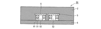
- the resin sheet 2 for electronic component sealing is used for manufacturing a resin-sealed semiconductor device (for example, the resin-sealed semiconductor device 50 shown in FIG. 6).
- the resin sheet 2 for sealing an electronic component has a moisture permeability of 300 g / m 2 ⁇ 24 hours or less under conditions of a temperature of 85 ° C., a humidity of 85%, and 168 hours when the thickness is 250 ⁇ m. 200 g / m 2 ⁇ 24 hours or less is preferable, and 100 g / m 2 ⁇ 24 hours or less is more preferable. Moreover, although the said water vapor transmission rate is so preferable that it is small, it is 1 g / m ⁇ 2 > * 24 hours or more, for example.
- the moisture permeability after thermosetting when the thickness is 250 ⁇ m is 300 g / m 2 ⁇ 24 hours or less under the conditions of a temperature of 85 ° C., a humidity of 85%, and 168 hours. Hard to reach. As a result, the reliability of the resin-encapsulated semiconductor device having the electronic component encapsulating resin sheet 2 can be improved.
- the resin sheet 2 for sealing an electronic component has a moisture permeability of 100 g / m 2 ⁇ 24 hours or less under conditions of a temperature of 60 ° C., a humidity of 90%, and 168 hours when the thickness is 250 ⁇ m. It is preferably 50 g / m 2 ⁇ 24 hours or less, and more preferably 20 g / m 2 ⁇ 24 hours or less. Moreover, although the said water vapor transmission rate is so preferable that it is small, it is 0.5 g / m ⁇ 2 > * 24 hours or more, for example.
- the moisture permeability after thermosetting is 100 g / m 2 ⁇ 24 hours or less under the conditions of a temperature of 60 ° C., a humidity of 90%, and 168 hours.
- the reliability of the resin-encapsulated semiconductor device having can be further improved.
- the resin composition for forming the resin sheet 2 for sealing an electronic component is not particularly limited as long as it can be used for sealing an electronic component (for example, the semiconductor chip 5).
- a component to E component The resin composition containing is mentioned as a preferable thing.
- the epoxy resin (component A) is not particularly limited.
- Various epoxy resins such as an epoxy resin, a phenol novolac type epoxy resin, and a phenoxy resin can be used. These epoxy resins may be used alone or in combination of two or more.
- a modified bisphenol A type epoxy resin having a flexible skeleton such as an acetal group or a polyoxyalkylene group is preferable, and a modified bisphenol A type epoxy resin having an acetal group is in a liquid state and is easy to handle. Therefore, it can be particularly preferably used.
- the content of the epoxy resin (component A) is preferably 1 to 10% by weight, and more preferably 2 to 5% by weight, based on the entire resin sheet for sealing electronic parts.
- the phenol resin (component B) is not particularly limited as long as it causes a curing reaction with the epoxy resin (component A).
- a phenol novolak resin, a phenol aralkyl resin, a biphenyl aralkyl resin, a dicyclopentadiene type phenol resin, a cresol novolak resin, a resole resin, or the like is used. These phenolic resins may be used alone or in combination of two or more.
- phenol resin those having a hydroxyl equivalent weight of 70 to 250 and a softening point of 50 to 110 ° C. are preferably used from the viewpoint of reactivity with the epoxy resin (component A), and above all, from the viewpoint of high curing reactivity.
- a phenol novolac resin can be preferably used. From the viewpoint of reliability, low hygroscopic materials such as phenol aralkyl resins and biphenyl aralkyl resins can also be suitably used.
- the blending ratio of the epoxy resin (component A) and the phenol resin (component B) is a hydroxyl group in the phenol resin (component B) with respect to 1 equivalent of the epoxy group in the epoxy resin (component A). It is preferable to blend so that the total amount becomes 0.7 to 1.5 equivalents, more preferably 0.9 to 1.2 equivalents.
- the elastomer (C component) used together with the epoxy resin (A component) and the phenol resin (B component) provides flexibility necessary for sealing the semiconductor chip 5 when the resin sheet for sealing electronic components is formed into a sheet shape.
- the structure is not particularly limited as long as it is imparted to the resin composition and exhibits such an action.
- various acrylic copolymers such as polyacrylates, styrene acrylate copolymers, butadiene rubber, styrene-butadiene rubber (SBR), ethylene-vinyl acetate copolymer (EVA), isoprene rubber, acrylonitrile rubber, etc. Polymers can be used.
- the epoxy resin (component A) it is easy to disperse in the epoxy resin (component A), and because the reactivity with the epoxy resin (component A) is high, the heat resistance and strength of the resulting resin sheet for sealing electronic components can be improved. From the viewpoint, it is preferable to use an acrylic copolymer. These may be used alone or in combination of two or more.
- the acrylic copolymer can be synthesized, for example, by radical polymerization of an acrylic monomer mixture having a predetermined mixing ratio by a conventional method.
- a method for radical polymerization a solution polymerization method in which an organic solvent is used as a solvent or a suspension polymerization method in which polymerization is performed while dispersing raw material monomers in water are used.
- polymerization initiator used in this case examples include 2,2′-azobisisobutyronitrile, 2,2′-azobis- (2,4-dimethylvaleronitrile), and 2,2′-azobis-4- Methoxy-2,4-dimethylvaleronitrile, other azo or diazo polymerization initiators, peroxide polymerization initiators such as benzoyl peroxide and methyl ethyl ketone peroxide are used.
- a dispersing agent such as polyacrylamide or polyvinyl alcohol.
- the content of the elastomer (component C) is preferably 1 to 10% by weight, and more preferably 2 to 5% by weight, based on the entire resin sheet for sealing electronic parts.
- the sheet can have flexibility and toughness.
- strength of a molded object required as a package can be expressed by content of an elastomer (C component) being 10 weight% or less.
- the weight ratio of the elastomer (component C) to the epoxy resin (component A) is preferably 0.3 to 2, and preferably 0.7 to 1.5. It is more preferable. By setting the weight ratio to 0.3 or more, toughness and flexibility can be imparted to the sheet. On the other hand, by setting the weight ratio to 2 or less, the reliability of the package after curing can be maintained.
- the inorganic filler (component D) is not particularly limited, and various conventionally known fillers can be used.
- various conventionally known fillers can be used.
- powders such as aluminum and silicon nitride. These may be used alone or in combination of two or more.
- silica powder from the viewpoint of low moisture permeability, and it is more preferable to use fused silica powder among silica powders.
- the fused silica powder include spherical fused silica powder and crushed fused silica powder. From the viewpoint of fluidity, it is particularly preferable to use a spherical fused silica powder.
- those having an average particle diameter in the range of 0.1 to 50 ⁇ m are preferably used, and those having a range of 0.3 to 25 ⁇ m are particularly preferable.
- the average particle diameter can be derived by, for example, using a sample arbitrarily extracted from the population and measuring it using a laser diffraction / scattering particle size distribution measuring apparatus.
- the content of the inorganic filler (component D) is preferably 70 to 93% by weight, more preferably 75 to 90% by weight, and more preferably 80 to 88% with respect to the entire resin sheet for sealing electronic parts. More preferably, it is% by weight. Since the inorganic filler has low moisture permeability, the moisture permeability of the electronic component sealing resin sheet 2 can be lowered by setting the content to 70% by weight or more. On the other hand, by setting the content of the inorganic filler to 93% by weight or less, the resin sheet 2 for sealing an electronic component can be easily formed into a sheet shape.
- the curing accelerator (component E) is not particularly limited as long as it allows curing of the epoxy resin and the phenol resin, but from the viewpoint of curability and storage stability, triphenylphosphine or tetraphenylphosphonium tetraphenyl. Organic phosphorus compounds such as borates and imidazole compounds are preferably used. These curing accelerators may be used alone or in combination with other curing accelerators.
- the content of the curing accelerator (component E) is preferably 0.1 to 5 parts by weight with respect to a total of 100 parts by weight of the epoxy resin (component A) and the phenol resin (component B).
- a flame retardant component may be added to the resin composition.
- the flame retardant composition include organophosphorus flame retardants such as phosphazene, various metal hydroxides such as aluminum hydroxide, magnesium hydroxide, iron hydroxide, calcium hydroxide, tin hydroxide, and complex metal hydroxides. Etc. can be used.
- Organophosphorous flame retardants are preferred from the viewpoint of dispersibility in the resin composition, but depending on the case, aluminum hydroxide or hydroxide may be used from the viewpoint of exhibiting flame retardancy with a relatively small addition amount or from a cost viewpoint. Sometimes magnesium is used. These may be used alone or in combination.
- the resin composition can contain other additives such as pigments such as carbon black as needed in addition to the above components.
- a resin composition is prepared by mixing the above-described components.
- the mixing method is not particularly limited as long as each component is uniformly dispersed and mixed. Thereafter, for example, a varnish in which each component is dissolved or dispersed in an organic solvent or the like is applied to form a sheet.
- a kneaded material may be prepared by directly kneading each compounding component with a kneader or the like, and the kneaded material thus obtained may be extruded to form a sheet.
- the above components A to E and other additives as necessary are mixed as appropriate according to a conventional method, and uniformly dissolved or dispersed in an organic solvent to prepare a varnish.
- the resin sheet 2 for electronic component sealing can be obtained by apply
- peeling sheets such as a polyester film. The release sheet peels at the time of sealing.
- the organic solvent is not particularly limited, and various conventionally known organic solvents such as methyl ethyl ketone, acetone, cyclohexanone, dioxane, diethyl ketone, toluene, and ethyl acetate can be used. These may be used alone or in combination of two or more. Usually, it is preferable to use an organic solvent so that the solid content concentration of the varnish is in the range of 30 to 60% by weight.
- the thickness of the sheet after drying the organic solvent is not particularly limited, but is usually preferably set to 5 to 100 ⁇ m, more preferably 20 to 70 ⁇ m, from the viewpoint of thickness uniformity and the amount of residual solvent. is there.
- the above components A to E and, if necessary, each component of other additives are mixed using a known method such as a mixer, and then kneaded to prepare a kneaded product.
- the method of melt kneading is not particularly limited, and examples thereof include a method of melt kneading with a known kneader such as a mixing roll, a pressure kneader, or an extruder.
- the kneading conditions are not particularly limited as long as the temperature is equal to or higher than the softening point of each component described above.
- thermosetting property of the epoxy resin it is preferably 40 to 140 ° C., more preferably The temperature is 60 to 120 ° C., and the time is, for example, 1 to 30 minutes, preferably 5 to 15 minutes. Thereby, a kneaded material can be prepared.
- the resin sheet 2 for electronic component sealing can be obtained by shape
- the resin sheet 2 for sealing an electronic component can be formed by extrusion molding without cooling the kneaded product after melt-kneading.
- Such an extrusion method is not particularly limited, and examples thereof include a T-die extrusion method, a roll rolling method, a roll kneading method, a co-extrusion method, and a calendar molding method.
- the extrusion temperature is not particularly limited as long as it is equal to or higher than the softening point of each component described above. However, considering the thermosetting property and moldability of the epoxy resin, for example, 40 to 150 ° C., preferably 50 to 140 ° C. Preferably, it is 70 to 120 ° C.
- the resin sheet 2 for electronic component sealing can be formed by the above.
- the inorganic filler is contained in an amount of 70 to 93% by weight based on the entire electronic component sealing resin sheet 2, it is preferably manufactured by kneading extrusion from the viewpoint of formability into a sheet. By producing by kneading extrusion, a uniform sheet with less voids (bubbles) can be obtained. As a result, low moisture permeability can be realized.
- the resin sheet 2 for encapsulating electronic parts obtained in this way may be laminated and used so as to have a desired thickness if necessary. That is, the sheet-like resin composition may be used in a single layer structure, or may be used as a laminate formed by laminating two or more multilayer structures.
- FIGS. 2 to 6 are schematic cross-sectional views for explaining the method for manufacturing the resin-encapsulated semiconductor device according to this embodiment.
- the manufacturing method of the semiconductor device includes at least a step of laminating a resin sheet for encapsulating electronic components from the semiconductor chip side so as to cover the semiconductor chip flip-chip connected on the adherend.
- the semiconductor wafer 4 is stuck on the pressure-sensitive adhesive layer 32 of the dicing tape 3 in which the pressure-sensitive adhesive layer 32 is laminated on the base material 31, and this is adhered and held and fixed ( Mounting process).
- the pressure-sensitive adhesive layer 32 is attached to the back surface of the semiconductor wafer 4.
- the back surface of the semiconductor wafer 4 means a surface opposite to the circuit surface (also referred to as a non-circuit surface or a non-electrode forming surface).
- the sticking method is not specifically limited, the method by pressure bonding is preferable.
- the crimping is usually performed while pressing with a pressing means such as a crimping roll.
- a dicing tape 3 a conventionally well-known thing can be used.
- Examples of the base material 31 include, for example, low density polyethylene, linear polyethylene, medium density polyethylene, high density polyethylene, very low density polyethylene, random copolymer polypropylene, block copolymer polypropylene, homopolyprolene, polybutene, and polymethyl.
- Polyolefin such as pentene, ethylene-vinyl acetate copolymer, ionomer resin, ethylene- (meth) acrylic acid copolymer, ethylene- (meth) acrylic acid ester (random, alternating) copolymer, ethylene-butene copolymer , Ethylene-hexene copolymer, polyurethane, polyester such as polyethylene terephthalate, polyethylene naphthalate, polycarbonate, polyimide, polyetheretherketone, polyimide, polyetherimide, polyamide, wholly aromatic polymer Amides, polyphenyl sulfide, aramid (paper), glass, glass cloth, fluorine resin, polyvinyl chloride, polyvinylidene chloride, cellulose resin, silicone resin, metal (foil) can also be used such as paper.
- polyester such as polyethylene terephthalate, polyethylene naphthalate, polycarbonate, polyimide, polyetheretherketone, polyimide
- the pressure-sensitive adhesive used for forming the pressure-sensitive adhesive layer 32 for example, a general pressure-sensitive pressure-sensitive adhesive such as an acrylic pressure-sensitive adhesive or a rubber-based pressure-sensitive adhesive can be used.
- the pressure-sensitive adhesive layer 32 can be formed of an ultraviolet curable pressure-sensitive adhesive.
- the ultraviolet curable pressure-sensitive adhesive can increase the degree of crosslinking by irradiation with ultraviolet rays and easily reduce its adhesive strength, and can be easily picked up when irradiated with ultraviolet rays after the dicing step.
- the semiconductor wafer 4 is diced. As a result, the semiconductor wafer 4 is cut into a predetermined size and divided into pieces (small pieces), whereby the semiconductor chip 5 is manufactured. Dicing is performed according to a conventional method from the circuit surface side of the semiconductor wafer 4, for example. It does not specifically limit as a dicing apparatus used at this process, A conventionally well-known thing can be used.
- the expanding can be performed using a conventionally known expanding apparatus.
- the expanding device has a donut-shaped outer ring that can push down the dicing tape 3 through the dicing ring, and an inner ring that has a smaller diameter than the outer ring and supports the dicing tape 3.
- the semiconductor chip 5 is picked up and peeled off from the dicing tape 3 as shown in FIG. 4.
- the pickup method is not particularly limited, and various conventionally known methods can be employed. For example, a method of pushing up the individual semiconductor chips 5 from the base 31 side with a needle and picking up the pushed-up semiconductor chips 5 with a pick-up device may be mentioned.
- the picked-up semiconductor chip 5 is fixed to an adherend such as a substrate by a flip chip bonding method (flip chip mounting method).
- the semiconductor chip 5 is always placed on the adherend 6 such that the circuit surface (also referred to as a surface, a circuit pattern formation surface, an electrode formation surface, etc.) of the semiconductor chip 5 faces the adherend 6.
- the circuit surface also referred to as a surface, a circuit pattern formation surface, an electrode formation surface, etc.
- the bump 51 formed on the circuit surface side of the semiconductor chip 5 is brought into contact with a bonding conductive material (solder or the like) 61 attached to the connection pad of the adherend 6 while pressing the conductive material.
- the semiconductor chip 5 By melting, it is possible to secure electrical continuity between the semiconductor chip 5 and the adherend 6 and fix the semiconductor chip 5 to the adherend 6 (flip chip bonding step). At this time, a gap is formed between the semiconductor chip 5 and the adherend 6, and the gap distance is generally about 15 ⁇ m to 300 ⁇ m. Note that after the semiconductor chip 5 is flip-chip bonded (flip chip connection) on the adherend 6, the facing surface and the gap between the semiconductor chip 5 and the adherend 6 may be cleaned. Further, the gap may be sealed by being filled with a sealing material (such as a sealing resin) depending on the use of the semiconductor device, or may be left as it is.
- a sealing material such as a sealing resin
- MEMS and surface acoustic wave filters such as acceleration sensors, pressure sensors, and gyro sensors
- SAW filters surface acoustic wave filters
- various substrates such as a lead frame and a circuit substrate (such as a wiring circuit substrate) can be used.
- the material of such a substrate is not particularly limited, and examples thereof include a ceramic substrate and a plastic substrate.
- the plastic substrate include an epoxy substrate, a bismaleimide triazine substrate, and a polyimide substrate.
- the material of the bump or the conductive material is not particularly limited, and for example, a tin-lead metal material, a tin-silver metal material, a tin-silver-copper metal material, a tin-zinc metal Materials, solders (alloys) such as tin-zinc-bismuth metal materials, gold metal materials, copper metal materials, and the like.
- the conductive material is melted to connect the bumps on the circuit surface side of the semiconductor chip 5 and the conductive material on the surface of the adherend 6.
- the temperature is usually about 260 ° C. (for example, 250 ° C. to 300 ° C.).
- a sealing step for sealing the gap between the flip chip bonded semiconductor chip 5 and the adherend 6 is performed.
- the sealing step is performed using an underfill sealing resin.
- the sealing conditions at this time are not particularly limited.
- the sealing resin is thermally cured by heating at 175 ° C. for 60 seconds to 90 seconds, but the present invention is not limited to this. For example, it can be cured at 165 ° C. to 185 ° C. for several minutes.
- the underfill sealing resin is not particularly limited as long as it is an insulating resin (insulating resin), and can be appropriately selected from sealing materials such as known sealing resins. An insulating resin is more preferable.
- the underfill sealing resin include a resin composition containing an epoxy resin.
- the epoxy resin include the epoxy resins exemplified above.
- the sealing resin for underfill using a resin composition containing an epoxy resin includes, as a resin component, a thermosetting resin other than an epoxy resin (such as a phenol resin) or a thermoplastic resin. It may be.
- a phenol resin it can utilize also as a hardening
- the electronic component sealing resin sheet 2 is stacked on the adherend 6 from the semiconductor chip 5 side so as to cover the semiconductor chip 5 (see FIG. 6).
- the electronic component sealing resin sheet 2 functions as a sealing resin for protecting the semiconductor chip 5 and its accompanying elements from the external environment.
- the method for laminating the resin sheet 2 for sealing an electronic component is not particularly limited, and a melt-kneaded product of a resin composition for forming the resin sheet for sealing an electronic component is extruded, and the extruded product is formed on the semiconductor chip 5 side.
- a method for forming and laminating a resin sheet for encapsulating electronic parts in a lump by placing and pressing on an adherend 6 from the substrate, and a resin composition for forming a resin sheet for encapsulating electronic parts Is applied to the adherend 6 from the semiconductor chip 5 side, and then dried, the resin composition is applied onto the release treatment sheet, and the coating film is dried to form the resin sheet 2 for sealing an electronic component.
- a method of transferring the resin sheet 2 for sealing an electronic component from the semiconductor chip 5 side onto the adherend 6 is exemplified.
- the resin sheet 2 for electronic component sealing can be laminated on the adherend 6 by a known method such as hot press or laminator.
- hot press conditions the temperature is, for example, 40 to 120 ° C., preferably 50 to 100 ° C.
- the pressure is, for example, 50 to 2500 kPa, preferably 100 to 2000 kPa
- the time is, for example, 0 3 to 10 minutes, preferably 0.5 to 5 minutes.
- it is preferable to press under reduced pressure conditions for example, 10 to 2000 Pa).
- the electronic component sealing resin sheet 2 is cured.
- the electronic component sealing resin sheet 2 is cured in a temperature range of 120 ° C. to 190 ° C., a heating time of 1 minute to 60 minutes, and a pressure of 0.1 MPa to 10 MPa.
- the resin-encapsulated semiconductor device 50 is obtained.
- the stationary semiconductor device 50 can be manufactured.
- the resin sheet for sealing an electronic component is used for manufacturing a flip-chip type semiconductor device.
- the resin sheet for sealing an electronic component of the present invention is not limited to this example, and can be used for manufacturing a semiconductor device in which the back surface of a semiconductor chip is attached to an adherend.
- the present invention is not limited to this example, and a flip chip type semiconductor back film is attached to the back surface of the semiconductor chip. May be attached.
- the flip chip type film for semiconductor back surface is used to protect the back surface (exposed back surface) of the semiconductor chip when the semiconductor chip is mounted on the substrate by flip chip bonding. Can be adopted.
- the resin sheet for sealing an electronic component is laminated from the semiconductor chip side so as to cover the semiconductor chip flip-chip connected to the adherend.
- the resin sheet for use may be laminated so as to cover not only the semiconductor chip but also other electronic components (for example, a capacitor, a resistor, etc.). That is, the resin sheet for encapsulating electronic components of the present invention is not limited to embedding semiconductor chips, and may be used for embedding other electronic components.
- Example 1 ⁇ Preparation of kneaded product of resin sheet for sealing electronic parts> (Example 1) The following components were kneaded with a biaxial kneader at 120 ° C. for 5 minutes to prepare a kneaded product.
- Component A epoxy resin: bisphenol F type epoxy resin (manufactured by Toto Kasei Co., Ltd., YSLV-80XY) 3.38 parts
- Component B phenol resin: phenol resin having a biphenylaralkyl skeleton (manufactured by Meiwa Kasei Co., Ltd., MEH7851SS) 3.58 parts
- Other components 1 Carbon black ( Made by Mitsubishi Chemical
- the kneaded product was extrusion-molded, and the extrusion-molded product was set to a certain thickness (250 ⁇ m in Example 1) by a vacuum press.
- the vacuum pressing was performed under the condition of pressing the inside of the chamber heated to 90 ° C. for 5 minutes (pressing pressure: 2 MPa). Thereby, the resin sheet for electronic component sealing which concerns on Example 1 was obtained. Then, it heated at 150 degreeC for 1 hour, and was hardened.
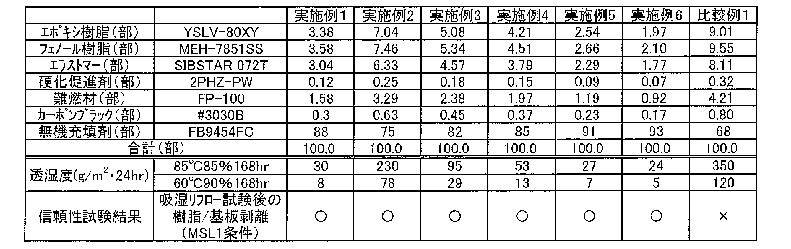
- Example 2 to 6 and Comparative Example 1 Resin sheets for electronic component sealing according to Examples 2 to 6 and Comparative Example 1 were obtained in the same manner as Example 1 except that the blending amount was changed as shown in Table 1. Then, it heated at 150 degreeC for 1 hour, and was hardened.
- Example 7 The following components were dissolved in 400 parts by weight of methyl ethyl ketone and blended so as to be uniform with a homogenizer.
- a component 1 (epoxy resin 1): (DIC, EXA-4850-150) 3.62 parts
- a component 2 (epoxy resin 2): novolac epoxy resin (Dainippon Ink, EPPN501HY) 1.53 parts
- B component phenol resin: (Gunei Chemical Co., Ltd., GS-200) 1.84 parts
- C component (elastomer) weight average molecular weight 750,000 consisting of 86 parts butyl acrylate, 7 parts acrylonitrile, 7 parts glycidyl methacrylate Acrylic copolymer 17.02 parts
- Other ingredients carbon black (manufactured by Mitsubishi Chemical Corporation, # 20) 0.74
- the compound was coated using a comma coater and dried with a solvent to obtain a resin sheet having a thickness of 50 ⁇ m.
- the resin sheet for electronic component sealing which concerns on Example 7 with a thickness of 250 micrometers was obtained by laminating
Landscapes
- Chemical & Material Sciences (AREA)
- Organic Chemistry (AREA)
- Inorganic Chemistry (AREA)
- Structures Or Materials For Encapsulating Or Coating Semiconductor Devices Or Solid State Devices (AREA)
- Engineering & Computer Science (AREA)
- Manufacturing & Machinery (AREA)
- Manufacture Of Macromolecular Shaped Articles (AREA)
- Microelectronics & Electronic Packaging (AREA)
- Materials Engineering (AREA)
- Health & Medical Sciences (AREA)
- Chemical Kinetics & Catalysis (AREA)
- Medicinal Chemistry (AREA)
- Polymers & Plastics (AREA)
Abstract
Description
なお、厚さが250μmではない場合には、下記式1により換算して、温度85℃、湿度85%、168時間の条件下における、厚さ250μmにした際の透湿度とする。
(式1) A-(250-D)×0.101
(A:透湿度、D:サンプル厚み(μm))
なお、厚さが250μmではない場合には、下記式2により換算して、温度60℃、湿度90%、168時間の条件下における、厚さ250μmにした際の透湿度とする。
(式2) A-(250-D)×0.010
(A:透湿度、D:サンプル厚み(μm)
図1で示されるように、電子部品封止用樹脂シート2は、シート状の形態を有している。電子部品封止用樹脂シート2は、樹脂封止型半導体装置(例えば、図6に示す樹脂封止型半導体装置50)の製造に使用される。
A成分:エポキシ樹脂
B成分:フェノール樹脂
C成分:エラストマー
D成分:無機充填剤
E成分:硬化促進剤
エポキシ樹脂(A成分)としては、特に限定されるものではない。例えば、トリフェニルメタン型エポキシ樹脂、クレゾールノボラック型エポキシ樹脂、ビフェニル型エポキシ樹脂、変性ビスフェノールA型エポキシ樹脂、ビスフェノールA型エポキシ樹脂、ビスフェノールF型エポキシ樹脂、変性ビスフェノールF型エポキシ樹脂、ジシクロペンタジエン型エポキシ樹脂、フェノールノボラック型エポキシ樹脂、フェノキシ樹脂等の各種のエポキシ樹脂を用いることができる。これらエポキシ樹脂は単独で用いてもよいし2種以上併用してもよい。
フェノール樹脂(B成分)は、エポキシ樹脂(A成分)との間で硬化反応を生起するものであれば特に限定されるものではない。例えば、フェノールノボラック樹脂、フェノールアラルキル樹脂、ビフェニルアラルキル樹脂、ジシクロペンタジエン型フェノール樹脂、クレゾールノボラック樹脂、レゾール樹脂、等が用いられる。これらフェノール樹脂は単独で用いてもよいし、2種以上併用してもよい。
エポキシ樹脂(A成分)及びフェノール樹脂(B成分)とともに用いられるエラストマー(C成分)は、電子部品封止用樹脂シートをシート状にした場合の半導体チップ5の封止に必要な可撓性を樹脂組成物に付与するものであり、このような作用を奏するものであれば特にその構造を限定するものではない。例えば、ポリアクリル酸エステル等の各種アクリル系共重合体、スチレンアクリレート系共重合体、ブタジエンゴム、スチレン-ブタジエンゴム(SBR)、エチレン-酢酸ビニルコポリマー(EVA)、イソプレンゴム、アクリロニトリルゴム等のゴム質重合体を用いることができる。中でも、エポキシ樹脂(A成分)へ分散させやすく、またエポキシ樹脂(A成分)との反応性も高いために、得られる電子部品封止用樹脂シートの耐熱性や強度を向上させることができるという観点から、アクリル系共重合体を用いることが好ましい。これらは単独で用いてもよいし、2種以上併せて用いてもよい。
無機質充填剤(D成分)は、特に限定されるものではなく、従来公知の各種充填剤を用いることができ、例えば、石英ガラス、タルク、シリカ(溶融シリカや結晶性シリカ等)、アルミナ、窒化アルミニウム、窒化珪素等の粉末が挙げられる。これらは単独で用いてもよいし、2種以上併用してもよい。
硬化促進剤(E成分)は、エポキシ樹脂とフェノール樹脂の硬化を進行させるものであれば特に限定されるものではないが、硬化性と保存性の観点から、トリフェニルホスフィンやテトラフェニルホスホニウムテトラフェニルボレート等の有機リン系化合物や、イミダゾール系化合物が好適に用いられる。これら硬化促進剤は、単独で用いても良いし、他の硬化促進剤と併用しても構わない。
また、樹脂組成物には、A成分からE成分に加えて、難燃剤成分を加えてもよい。難燃剤組成分としては、例えばホスファゼンなどの有機リン系難燃剤、水酸化アルミニウム、水酸化マグネシウム、水酸化鉄、水酸化カルシウム、水酸化スズ、複合化金属水酸化物等の各種金属水酸化物などを用いることができる。樹脂組成物中での分散性の観点から有機リン系難燃剤が好ましいが、場合によっては、比較的少ない添加量で難燃性を発揮できる観点や、コスト的な観点から水酸化アルミニウム又は水酸化マグネシウムを用いる場合もある。これらは単独で用いても、組合せで用いても良い。
電子部品封止用樹脂シート2の作製方法について、電子部品封止用樹脂シート2がシート状熱硬化型樹脂層である場合の手順を以下に説明する。
次に、本実施形態に係る樹脂封止型半導体装置の製造方法について、図2~図6を参照しながら以下に説明する。図2~図6は、本実施形態に係る樹脂封止型半導体装置の製造方法を説明するための断面模式図である。
先ず、図2で示されるように、基材31上に粘着剤層32が積層されたダイシングテープ3の粘着剤層32上に半導体ウエハ4を貼着して、これを接着保持させ固定する(マウント工程)。粘着剤層32は、半導体ウエハ4の裏面に貼着される。半導体ウエハ4の裏面とは、回路面とは反対側の面(非回路面、非電極形成面などとも称される)を意味する。貼着方法は特に限定されないが、圧着による方法が好ましい。圧着は、通常、圧着ロール等の押圧手段により押圧しながら行われる。なお、ダイシングテープ3としては、従来公知のものを使用することができる。
次に、図3で示されるように、半導体ウエハ4のダイシングを行う。これにより、半導体ウエハ4を所定のサイズに切断して個片化(小片化)し、半導体チップ5を製造する。ダイシングは、例えば、半導体ウエハ4の回路面側から常法に従い行われる。本工程で用いるダイシング装置としては特に限定されず、従来公知のものを用いることができる。
ダイシングテープ3に接着固定された半導体チップ5を回収する為に、図4で示されるように、半導体チップ5のピックアップを行って、半導体チップ5をダイシングテープ3より剥離させる。ピックアップの方法としては特に限定されず、従来公知の種々の方法を採用できる。例えば、個々の半導体チップ5を基材31側からニードルによって突き上げ、突き上げられた半導体チップ5をピックアップ装置によってピックアップする方法等が挙げられる。
ピックアップした半導体チップ5は、図5で示されるように、基板等の被着体に、フリップチップボンディング方式(フリップチップ実装方式)により固定させる。具体的には、半導体チップ5を、半導体チップ5の回路面(表面、回路パターン形成面、電極形成面などとも称される)が被着体6と対向する形態で、被着体6に常法に従い固定させる。例えば、半導体チップ5の回路面側に形成されているバンプ51を、被着体6の接続パッドに被着された接合用の導電材(半田など)61に接触させて押圧しながら導電材を溶融させることにより、半導体チップ5と被着体6との電気的導通を確保し、半導体チップ5を被着体6に固定させることができる(フリップチップボンディング工程)。このとき、半導体チップ5と被着体6との間には空隙が形成されており、その空隙間距離は、一般的に15μm~300μm程度である。尚、半導体チップ5を被着体6上にフリップチップボンディング(フリップチップ接続)した後は、半導体チップ5と被着体6との対向面や間隙を洗浄してもよい。また、該空隙は、半導体装置の用途に応じて封止材(封止樹脂など)を充填させて封止してもよく、空隙のままとしておいてもよい。ただし、加速度センサ、圧力センサ、ジャイロセンサ等のMEMSや表面弾性波フィルター(SAWフィルター)においては、構造上、被着体と半導体チップとの間に空隙が形成されている必要があるため、このような用途においては、空隙のままとしておく。
電子部品封止用樹脂シートの積層工程では、半導体チップ5を覆うように半導体チップ5側から電子部品封止用樹脂シート2を被着体6上に積層する(図6参照)。この電子部品封止用樹脂シート2は、半導体チップ5及びそれに付随する要素を外部環境から保護するための封止樹脂として機能する。
(実施例1)
以下の成分を2軸混練り機により、120℃で5分間混練し、混練物を調製した。
B成分(フェノール樹脂):ビフェニルアラルキル骨格を有するフェノール樹脂(明和化成社製、MEH7851SS) 3.58部
C成分(エラストマー):熱可塑性エラストマー((株)カネカ社製、製品名:SIBSTER 072T) 3.04部
D成分(無機充填剤):球状シリカ(電気化学工業社製、製品名FB-9454FC、平均粒子径20μm) 88部
E成分(硬化促進剤):硬化触媒としてのイミダゾール系触媒(四国化成工業(株)製2PHZ-PW) 0.119部
その他成分1:カーボンブラック(三菱化学社製、#3030B) 0.3部
その他成分2:難燃剤(フェノキシホスファゼンオリゴマー、製品名:FP-100、伏見製薬所製) 1.58部
配合量を表1の通りに変更した以外は、実施例1と同様にして実施例2~6、及び、比較例1に係るに電子部品封止用樹脂シートを得た。その後、150℃で1時間加熱し、硬化させた。
以下の成分を400重量部のメチルエチルケトンに溶解し、ホモジナイザーにて均一になるように配合した。
A成分2(エポキシ樹脂2):ノボラック型エポキシ樹脂(大日本インキ社製、EPPN501HY) 1.53部
B成分(フェノール樹脂):(群栄化学製、GS-200) 1.84部
C成分(エラストマー):アクリル酸ブチル86部、アクリロニトリル7部、メタクリル酸グリシジル7部からなる重量平均分子量75万のアクリル系共重合体
17.02部
D成分(無機充填剤):球状シリカ(アドマテックス社製、SO-E2、平均粒子径0.5μm) 75部
E成分(硬化促進剤):硬化触媒としてのイミダゾール系触媒(四国化成工業(株)製2PHZ-PW) 0.25部
その他成分:カーボンブラック(三菱化学社製、#20) 0.74部
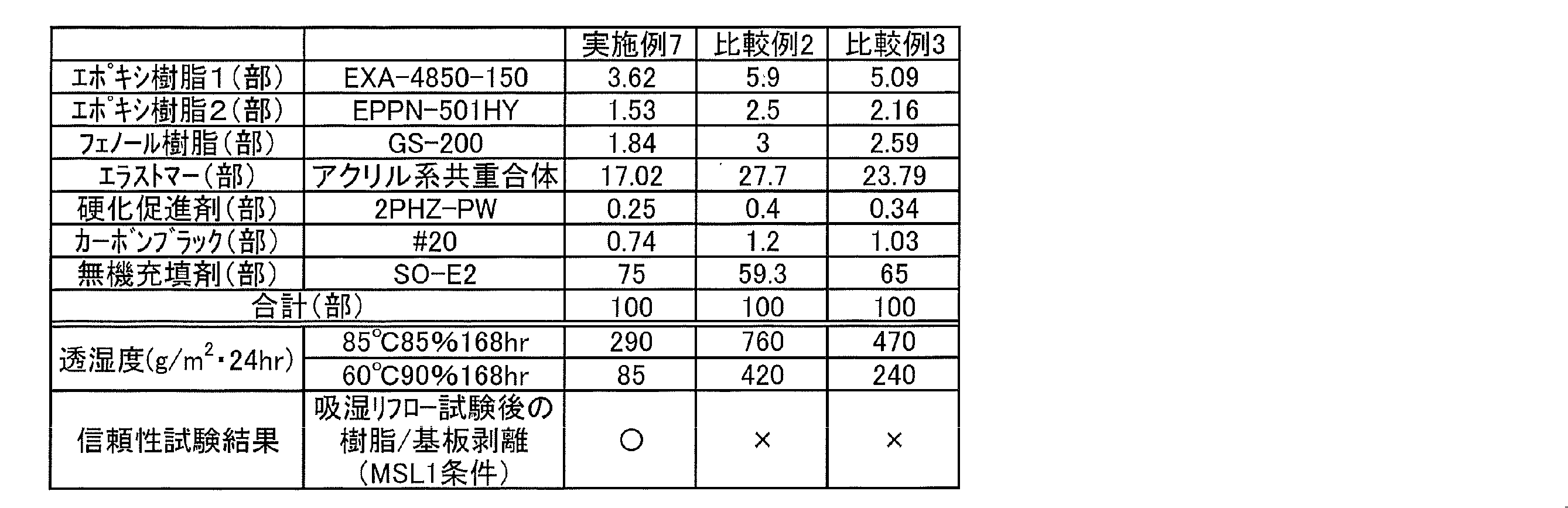
配合量を表2の通りに変更した以外は、実施例7と同様にして比較例2、及び、比較例3に係るに電子部品封止用樹脂シートを得た。その後、150℃で1時間加熱し、硬化させた。
JIS Z 0208(カップ法)の規定に準じて、実施例、比較例で作成した電子部品封止用樹脂シート(熱硬化後)の透湿度を測定した。測定条件は下記の通りとした。結果を表1、及び、表2に示す。
(測定条件1)
温度85℃、湿度85%、168時間、電子部品封止用樹脂シートの厚さ:250μm
(測定条件2)
温度60℃、湿度90%、168時間、電子部品封止用樹脂シートの厚さ:250μm
厚さ0.5mmのアルミナ基板に、1mmx1mmx0.2mmtサイズのSiチップ25個(5列×5列、チップ間隔は0.5mmとした)が、金バンプによって超音波接続されたもの(チップ下面と基板とのギャップ:20μm)を準備した。
次に、実施例、及び、比較例にて作製した電子部品封止用樹脂シートを用いて、真空プレスにより上記Siチップの封止を行い(封止条件:50℃、1MPa、1分、真空度1000Pa)、150℃で1時間硬化させた。これにより各チップの下部に空隙が形成された状態の硬化物を得た。その後、ダイシングにより個別のパッケージに分割した。これをJEDECのMSL1(Moisture Sensitivity Level)試験に準拠した手法で、85℃、85%、168時間の条件にて吸湿させた。その後、IRリフロー装置にて260℃×3回の吸湿リフロー試験を行った。試験後のパッケージを超音波顕微鏡で観察し、基板、樹脂間に剥離が観察されたものを×、観察されなかったものを○とした。結果を表1、及び、表2に示す。
3 ダイシングテープ
31 基材
32 粘着剤層
4 半導体ウエハ
5 半導体チップ
51 半導体チップ5の回路面側に形成されているバンプ
52 空隙
6 被着体
61 被着体6の接続パッドに被着された接合用の導電材
Claims (6)
- 樹脂封止型半導体装置の製造に使用される電子部品封止用樹脂シートであって、
無機充填剤を電子部品封止用樹脂シート全体に対して、70~93重量%含み、
厚さ250μmにした際の熱硬化後の透湿度が、温度85℃、湿度85%、168時間の条件下において、300g/m2・24時間以下であることを特徴とする電子部品封止用樹脂シート。 - 厚さ250μmにした際の熱硬化後の透湿度が、温度60℃、湿度90%、168時間の条件下において、100g/m2・24時間以下であることを特徴とする請求項1に記載の電子部品封止用樹脂シート。
- 混練押出により製造されていることを特徴とする請求項1又は2に記載の電子部品封止用樹脂シート。
- 被着体と、
前記被着体にフリップチップ接続された半導体チップと、
前記半導体チップを封止する電子部品封止用樹脂シートと
を備え、
前記電子部品封止用樹脂シートは、
無機充填剤を電子部品封止用樹脂シート全体に対して、70~93重量%含み、厚さ250μmにした際の熱硬化後の透湿度が、温度85℃、湿度85%、168時間の条件下において、300g/m2・24時間以下であり、
前記被着体と前記半導体チップとの間には、空隙が形成されていることを特徴とする樹脂封止型半導体装置。 - 請求項1~3のいずれか1に記載の電子部品封止用樹脂シートを有する樹脂封止型半導体装置。
- 樹脂封止型半導体装置の製造方法であって、
被着体上にフリップチップ接続された半導体チップを覆うように、半導体チップ側から電子部品封止用樹脂シートを積層する工程を具備し、
前記電子部品封止用樹脂シートは、
無機充填剤を電子部品封止用樹脂シート全体に対して、70~93重量%含み、
厚さ250μmにした際の熱硬化後の透湿度が、温度85℃、湿度85%、168時間の条件下において、300g/m2・24時間以下であることを特徴とする樹脂封止型半導体装置の製造方法。
Priority Applications (3)
| Application Number | Priority Date | Filing Date | Title |
|---|---|---|---|
| CN201480008390.5A CN105190867A (zh) | 2013-02-14 | 2014-02-13 | 电子部件密封用树脂片、树脂密封型半导体装置及树脂密封型半导体装置的制造方法 |
| SG11201505837RA SG11201505837RA (en) | 2013-02-14 | 2014-02-13 | Resin sheet for sealing electronic component, resin-sealed semiconductor device, and production method for resin-sealed semiconductor device |
| KR1020157025085A KR20150119265A (ko) | 2013-02-14 | 2014-02-13 | 전자 부품 봉지용 수지 시트, 수지 봉지형 반도체 장치, 및 수지 봉지형 반도체 장치의 제조 방법 |
Applications Claiming Priority (2)
| Application Number | Priority Date | Filing Date | Title |
|---|---|---|---|
| JP2013026935A JP6228734B2 (ja) | 2013-02-14 | 2013-02-14 | 電子部品封止用樹脂シート、樹脂封止型半導体装置、及び、樹脂封止型半導体装置の製造方法 |
| JP2013-026935 | 2013-02-14 |
Publications (1)
| Publication Number | Publication Date |
|---|---|
| WO2014126147A1 true WO2014126147A1 (ja) | 2014-08-21 |
Family
ID=51354146
Family Applications (1)
| Application Number | Title | Priority Date | Filing Date |
|---|---|---|---|
| PCT/JP2014/053318 Ceased WO2014126147A1 (ja) | 2013-02-14 | 2014-02-13 | 電子部品封止用樹脂シート、樹脂封止型半導体装置、及び、樹脂封止型半導体装置の製造方法 |
Country Status (6)
| Country | Link |
|---|---|
| JP (1) | JP6228734B2 (ja) |
| KR (1) | KR20150119265A (ja) |
| CN (1) | CN105190867A (ja) |
| SG (1) | SG11201505837RA (ja) |
| TW (1) | TWI624914B (ja) |
| WO (1) | WO2014126147A1 (ja) |
Cited By (2)
| Publication number | Priority date | Publication date | Assignee | Title |
|---|---|---|---|---|
| JPWO2016158760A1 (ja) * | 2015-03-31 | 2017-06-22 | 東レ株式会社 | 電子部品用樹脂シート、保護フィルム付電子部品用樹脂シートならびに半導体装置およびその製造方法 |
| US20210403765A1 (en) * | 2018-11-14 | 2021-12-30 | Nagase Chemtex Corporation | Curable resin composition and curable sheet |
Families Citing this family (3)
| Publication number | Priority date | Publication date | Assignee | Title |
|---|---|---|---|---|
| JP5976073B2 (ja) * | 2014-11-07 | 2016-08-23 | 日東電工株式会社 | 半導体装置の製造方法 |
| JP7257731B2 (ja) * | 2016-12-28 | 2023-04-14 | 日東電工株式会社 | 樹脂シート |
| CN107403771A (zh) * | 2017-08-21 | 2017-11-28 | 嘉盛半导体(苏州)有限公司 | 半导体封装结构及其封装方法 |
Citations (4)
| Publication number | Priority date | Publication date | Assignee | Title |
|---|---|---|---|---|
| JPH08255806A (ja) * | 1995-03-17 | 1996-10-01 | Toshiba Corp | 樹脂封止型半導体装置の製造方法 |
| JP2006032478A (ja) * | 2004-07-13 | 2006-02-02 | Nippon Steel Chem Co Ltd | 半導体装置の製造方法 |
| WO2007097022A1 (ja) * | 2006-02-27 | 2007-08-30 | Sumitomo Bakelite Co., Ltd. | 接着フィルム |
| WO2012020688A1 (ja) * | 2010-08-12 | 2012-02-16 | ダイセル化学工業株式会社 | 低透湿性樹脂組成物及びその硬化物 |
Family Cites Families (6)
| Publication number | Priority date | Publication date | Assignee | Title |
|---|---|---|---|---|
| JP3022135B2 (ja) * | 1994-01-26 | 2000-03-15 | 信越化学工業株式会社 | エポキシ樹脂組成物 |
| JP4150466B2 (ja) * | 1998-06-02 | 2008-09-17 | 日東電工株式会社 | 半導体封止用樹脂組成物およびそれを用いた半導体装置ならびに半導体装置の製法 |
| JP5426511B2 (ja) * | 2009-11-30 | 2014-02-26 | パナソニック株式会社 | 封止用エポキシ樹脂組成物シート及びこれを用いて封止した中空型デバイス |
| JP5861838B2 (ja) * | 2010-06-24 | 2016-02-16 | 日産化学工業株式会社 | 結晶化促進方法及び成形物の製造方法 |
| JP2012046657A (ja) * | 2010-08-27 | 2012-03-08 | Idemitsu Kosan Co Ltd | 半導体封止用エポキシ樹脂成形材料及び蓄熱性成形体 |
| JP2013007028A (ja) * | 2011-05-20 | 2013-01-10 | Nitto Denko Corp | 封止用シートおよび電子部品装置 |
-
2013
- 2013-02-14 JP JP2013026935A patent/JP6228734B2/ja not_active Ceased
-
2014
- 2014-02-13 SG SG11201505837RA patent/SG11201505837RA/en unknown
- 2014-02-13 WO PCT/JP2014/053318 patent/WO2014126147A1/ja not_active Ceased
- 2014-02-13 KR KR1020157025085A patent/KR20150119265A/ko not_active Withdrawn
- 2014-02-13 CN CN201480008390.5A patent/CN105190867A/zh active Pending
- 2014-02-14 TW TW103104995A patent/TWI624914B/zh active
Patent Citations (4)
| Publication number | Priority date | Publication date | Assignee | Title |
|---|---|---|---|---|
| JPH08255806A (ja) * | 1995-03-17 | 1996-10-01 | Toshiba Corp | 樹脂封止型半導体装置の製造方法 |
| JP2006032478A (ja) * | 2004-07-13 | 2006-02-02 | Nippon Steel Chem Co Ltd | 半導体装置の製造方法 |
| WO2007097022A1 (ja) * | 2006-02-27 | 2007-08-30 | Sumitomo Bakelite Co., Ltd. | 接着フィルム |
| WO2012020688A1 (ja) * | 2010-08-12 | 2012-02-16 | ダイセル化学工業株式会社 | 低透湿性樹脂組成物及びその硬化物 |
Cited By (3)
| Publication number | Priority date | Publication date | Assignee | Title |
|---|---|---|---|---|
| JPWO2016158760A1 (ja) * | 2015-03-31 | 2017-06-22 | 東レ株式会社 | 電子部品用樹脂シート、保護フィルム付電子部品用樹脂シートならびに半導体装置およびその製造方法 |
| US20210403765A1 (en) * | 2018-11-14 | 2021-12-30 | Nagase Chemtex Corporation | Curable resin composition and curable sheet |
| US11718770B2 (en) * | 2018-11-14 | 2023-08-08 | Nagase Chemtex Corporation | Curable resin composition and curable sheet |
Also Published As
| Publication number | Publication date |
|---|---|
| TWI624914B (zh) | 2018-05-21 |
| JP2014156516A (ja) | 2014-08-28 |
| KR20150119265A (ko) | 2015-10-23 |
| SG11201505837RA (en) | 2015-09-29 |
| JP6228734B2 (ja) | 2017-11-08 |
| TW201442166A (zh) | 2014-11-01 |
| CN105190867A (zh) | 2015-12-23 |
Similar Documents
| Publication | Publication Date | Title |
|---|---|---|
| TWI849115B (zh) | 接著劑用組成物、膜狀接著劑及其製造方法、以及使用膜狀接著劑之半導體封裝及其製造方法 | |
| JP6018967B2 (ja) | 熱硬化性封止樹脂シート及び電子部品パッケージの製造方法 | |
| TWI824195B (zh) | 切晶黏晶膜與使用其之半導體封裝及其製造方法 | |
| JP2009091389A (ja) | 中空型デバイス封止用樹脂組成物シートおよびそれを用いて封止した中空型デバイス | |
| KR102750581B1 (ko) | 열전도성 필름형 접착제, 반도체 패키지 및 그 제조 방법 | |
| JP6282626B2 (ja) | 中空型電子デバイス封止用シート、及び、中空型電子デバイスパッケージの製造方法 | |
| TWI828076B (zh) | 切晶黏晶膜及其製造方法、以及半導體封裝及其製造方法 | |
| JP6228734B2 (ja) | 電子部品封止用樹脂シート、樹脂封止型半導体装置、及び、樹脂封止型半導体装置の製造方法 | |
| US20240084172A1 (en) | Adhesive composition, film adhesive, and semiconductor package using film adhesive and producing method thereof | |
| WO2015060106A1 (ja) | 半導体パッケージの製造方法 | |
| TWI906612B (zh) | 接著劑用組成物及膜狀接著劑、以及使用了膜狀接著劑之半導體封裝及其製造方法 | |
| TWI844320B (zh) | 導熱性膜狀接著劑用組成物及導熱性膜狀接著劑、以及使用導熱性膜狀接著劑之半導體封裝之製造方法 | |
| JP2016096308A (ja) | 半導体装置の製造方法 | |
| CN112885790B (zh) | 电子器件密封用片和电子器件封装件的制造方法 | |
| US20240150622A1 (en) | Adhesive composition and film adhesive, and semiconductor package using film adhesive and producing method thereof | |
| CN115413363B (zh) | 切晶粘晶膜及其制造方法、以及半导体封装及其制造方法 | |
| JP2016136566A (ja) | 中空型電子デバイス封止用シート | |
| JP6283624B2 (ja) | 中空型電子デバイス封止用シート、中空型電子デバイスパッケージの製造方法、及び、中空型電子デバイスパッケージ | |
| JP2018104649A (ja) | 樹脂シート | |
| TWI828455B (zh) | 接著劑用組成物及膜狀接著劑、以及使用膜狀接著劑之半導體封裝及其製造方法 | |
| HK40059508A (en) | Dicing die attach film, semiconductor package using dicing die attach film, and method for manufacturing semiconductor package | |
| JP7257731B2 (ja) | 樹脂シート | |
| TW202302799A (zh) | 熱傳導性膜狀接著劑、半導體封裝及其製造方法 | |
| HK40077350A (en) | Dicing die attach film and method for producing same, and semiconductor package and method for producing same | |
| HK40097888A (zh) | 导热性膜状粘接剂、半导体封装及其制造方法 |
Legal Events
| Date | Code | Title | Description |
|---|---|---|---|
| WWE | Wipo information: entry into national phase |
Ref document number: 201480008390.5 Country of ref document: CN |
|
| 121 | Ep: the epo has been informed by wipo that ep was designated in this application |
Ref document number: 14752023 Country of ref document: EP Kind code of ref document: A1 |
|
| NENP | Non-entry into the national phase |
Ref country code: DE |
|
| ENP | Entry into the national phase |
Ref document number: 20157025085 Country of ref document: KR Kind code of ref document: A |
|
| 122 | Ep: pct application non-entry in european phase |
Ref document number: 14752023 Country of ref document: EP Kind code of ref document: A1 |