WO2014125943A1 - 光学センサヘッド、および光学センサシステム - Google Patents
光学センサヘッド、および光学センサシステム Download PDFInfo
- Publication number
- WO2014125943A1 WO2014125943A1 PCT/JP2014/052304 JP2014052304W WO2014125943A1 WO 2014125943 A1 WO2014125943 A1 WO 2014125943A1 JP 2014052304 W JP2014052304 W JP 2014052304W WO 2014125943 A1 WO2014125943 A1 WO 2014125943A1
- Authority
- WO
- WIPO (PCT)
- Prior art keywords
- light
- reflecting surface
- optical sensor
- hole
- detector
- Prior art date
- Legal status (The legal status is an assumption and is not a legal conclusion. Google has not performed a legal analysis and makes no representation as to the accuracy of the status listed.)
- Ceased
Links
Images





Classifications
-
- G—PHYSICS
- G01—MEASURING; TESTING
- G01N—INVESTIGATING OR ANALYSING MATERIALS BY DETERMINING THEIR CHEMICAL OR PHYSICAL PROPERTIES
- G01N21/00—Investigating or analysing materials by the use of optical means, i.e. using sub-millimetre waves, infrared, visible or ultraviolet light
- G01N21/62—Systems in which the material investigated is excited whereby it emits light or causes a change in wavelength of the incident light
- G01N21/63—Systems in which the material investigated is excited whereby it emits light or causes a change in wavelength of the incident light optically excited
- G01N21/65—Raman scattering
- G01N21/658—Raman scattering enhancement Raman, e.g. surface plasmons
-
- G—PHYSICS
- G01—MEASURING; TESTING
- G01N—INVESTIGATING OR ANALYSING MATERIALS BY DETERMINING THEIR CHEMICAL OR PHYSICAL PROPERTIES
- G01N21/00—Investigating or analysing materials by the use of optical means, i.e. using sub-millimetre waves, infrared, visible or ultraviolet light
- G01N21/75—Systems in which material is subjected to a chemical reaction, the progress or the result of the reaction being investigated
- G01N21/77—Systems in which material is subjected to a chemical reaction, the progress or the result of the reaction being investigated by observing the effect on a chemical indicator
- G01N21/7703—Systems in which material is subjected to a chemical reaction, the progress or the result of the reaction being investigated by observing the effect on a chemical indicator using reagent-clad optical fibres or optical waveguides
- G01N21/7746—Systems in which material is subjected to a chemical reaction, the progress or the result of the reaction being investigated by observing the effect on a chemical indicator using reagent-clad optical fibres or optical waveguides the waveguide coupled to a cavity resonator
-
- G—PHYSICS
- G01—MEASURING; TESTING
- G01N—INVESTIGATING OR ANALYSING MATERIALS BY DETERMINING THEIR CHEMICAL OR PHYSICAL PROPERTIES
- G01N21/00—Investigating or analysing materials by the use of optical means, i.e. using sub-millimetre waves, infrared, visible or ultraviolet light
- G01N21/17—Systems in which incident light is modified in accordance with the properties of the material investigated
- G01N21/41—Refractivity; Phase-affecting properties, e.g. optical path length
-
- G—PHYSICS
- G01—MEASURING; TESTING
- G01N—INVESTIGATING OR ANALYSING MATERIALS BY DETERMINING THEIR CHEMICAL OR PHYSICAL PROPERTIES
- G01N21/00—Investigating or analysing materials by the use of optical means, i.e. using sub-millimetre waves, infrared, visible or ultraviolet light
- G01N21/75—Systems in which material is subjected to a chemical reaction, the progress or the result of the reaction being investigated
- G01N21/77—Systems in which material is subjected to a chemical reaction, the progress or the result of the reaction being investigated by observing the effect on a chemical indicator
- G01N2021/7769—Measurement method of reaction-produced change in sensor
- G01N2021/7776—Index
-
- G—PHYSICS
- G01—MEASURING; TESTING
- G01N—INVESTIGATING OR ANALYSING MATERIALS BY DETERMINING THEIR CHEMICAL OR PHYSICAL PROPERTIES
- G01N21/00—Investigating or analysing materials by the use of optical means, i.e. using sub-millimetre waves, infrared, visible or ultraviolet light
- G01N21/17—Systems in which incident light is modified in accordance with the properties of the material investigated
- G01N21/55—Specular reflectivity
- G01N21/552—Attenuated total reflection
- G01N21/553—Attenuated total reflection and using surface plasmons
-
- G—PHYSICS
- G01—MEASURING; TESTING
- G01N—INVESTIGATING OR ANALYSING MATERIALS BY DETERMINING THEIR CHEMICAL OR PHYSICAL PROPERTIES
- G01N2201/00—Features of devices classified in G01N21/00
- G01N2201/06—Illumination; Optics
- G01N2201/061—Sources
- G01N2201/06113—Coherent sources; lasers
-
- G—PHYSICS
- G01—MEASURING; TESTING
- G01N—INVESTIGATING OR ANALYSING MATERIALS BY DETERMINING THEIR CHEMICAL OR PHYSICAL PROPERTIES
- G01N2201/00—Features of devices classified in G01N21/00
- G01N2201/06—Illumination; Optics
- G01N2201/068—Optics, miscellaneous
-
- G—PHYSICS
- G01—MEASURING; TESTING
- G01N—INVESTIGATING OR ANALYSING MATERIALS BY DETERMINING THEIR CHEMICAL OR PHYSICAL PROPERTIES
- G01N2201/00—Features of devices classified in G01N21/00
- G01N2201/08—Optical fibres; light guides
Definitions
- the present invention relates to an optical sensor head and an optical sensor system.
- a method of detecting a change in the resonance state of an optical resonator is used in various fields because it has high sensitivity and does not require a marker.
- the return light from the optical recording medium is returned to the semiconductor laser, the oscillation state of the semiconductor laser is changed, and this change is detected by a monitor PD (Photodetector).
- Patent Document 2 as a vibration detector, a vibrator is formed integrally with a semiconductor laser and a monitor PD, intensity modulation is applied to the oscillation state of the semiconductor laser by return light from the vibrator, and a signal detected by the monitor PD is detected. By analyzing this modulation, the change in the natural frequency of the vibrator and the pressure, temperature, displacement, flow rate, and the like, which are the causes, are measured.
- Patent Document 3 in a recording apparatus that uses a semiconductor laser element provided with a metal film having an exit window on an end face and records with near-field light generated at the exit window, reflected light from the recording medium of near-field light. Recording medium using the change in voltage generated between the current injection electrodes to the semiconductor laser element or the change in light intensity of the semiconductor laser element emitted from the side opposite to the end face provided with the metal film due to the return to the semiconductor laser element Is playing.
- the surface plasmon sensor that detects the refractive index of the metal film surface by surface plasmon resonance (resonance of incident light and vibration of electrons in the metal) mainly has high sensitivity and does not require a marker. It is used for research purposes in the bio field.
- a method using a resonator has been proposed in order to perform detection with a small size and high sensitivity.
- a microresonator is incorporated in a part of a planar waveguide, and a change in spectral response due to a change in refractive index on the surface of the microresonator is detected.
- This microresonator is made of a metal thin film, and the reflection part uses DBR (Distributed Bragg Reflector) reflection by a periodic structure, and is a resonator for surface plasmon waves.
- DBR Distributed Bragg Reflector
- a metal fine particle layer having a size capable of exciting localized surface plasmon resonance is formed on an end face of an optical fiber, and a molecule complementary to a detection target molecule is formed on the surface of the metal fine particle layer.
- a localized surface plasmon sensor having a molecular layer formed thereon is disclosed. This localized surface plasmon sensor detects a molecule to be detected that is adsorbed or bound to the complementary molecule using a change in light reflected or scattered from the end face of the optical fiber.
- Patent Document 1 since the optical recording medium is separated from the semiconductor laser, high-precision adjustment is required to return the light amount necessary for reproduction to the semiconductor laser, and the position due to change with time is also required. Since it must be structured to prevent deviation, it leads to higher costs.
- Patent Document 2 an oscillator having a high aspect ratio must be formed on the same substrate close to the semiconductor laser, and accuracy is required in masking and etching. Further, since the natural frequency must be detected, signal processing after detection is complicated.
- Patent Document 4 since a resonator having a length of 2 to 10 microns is used, a surface plasmon wave that is a damped wave is lost inside the resonator, and an improvement in sensitivity cannot be expected. In addition, there is a limit to downsizing as a separate light source is required.
- Patent Document 3 is for reproducing a change in reflectance of near-field light on a recording medium located away from a metal film having an exit window, and uses near-field light spreading outward from the exit window. is doing.
- This system is configured to be influenced by the outside of the through hole.
- the detection range is too wide for molecular level detection.
- Patent Document 5 has low sensitivity because it does not use a resonator. Further, in this sensor, a loss of light intensity occurs when the light from the light source is coupled to the optical fiber.
- An object of the present invention is to provide an optical sensor system capable of high sensitivity and miniaturization, as well as high sensitivity and miniaturization, being hardly affected by the outside of the through hole, and having a detection range that is not too wide.
- An optical sensor head and an optical sensor system including the same are provided.
- the optical sensor system of the present invention includes a first reflecting surface, a second reflecting surface facing the first reflecting surface, and the first reflecting surface and the second reflecting surface.
- a light emitting device having a waveguide provided between, a reactant formed on the first reflecting surface, and light emitted from one of the first reflecting surface and the second reflecting surface.
- An optical sensor system comprising: a first detector that detects light intensity; and a calculation unit that calculates an environmental parameter on the first reflection surface based on the light intensity detected by the first detector. , The reflectance R 1 of the first reflecting surface and the light intensity P (R 1 ) detected by the detector, Satisfy the relationship.
- the optical sensor head of the present invention includes a first reflecting surface, a second reflecting surface facing the first reflecting surface, and the first reflecting surface and the second reflecting surface.
- a light-emitting device provided with a waveguide provided between, a light-shielding film provided on the first reflecting surface, provided with a through-hole for generating near-field light, and the first or
- An optical sensor head comprising a detector that detects a light intensity of light emitted from the light emitting device through a second reflecting surface, wherein the opening area of the through hole on the light emitting surface of the light shielding film Is larger than the opening area of the through hole on the facing surface of the light shielding film facing the first reflecting surface.
- the conventional optical sensor system here means “a system that detects the amount of change in environmental parameters from reflected light or transmitted light when a reactant is irradiated with light”, details of which will be described later. To do.
- the light intensity distribution in the through hole is weak in the vicinity of the light exit surface and strong in the vicinity of the opposing surface, so that it is not easily affected by the outside of the through hole, and the through hole Only the refractive index change inside the hole can be detected with good sensitivity. For this reason, if the opening size on the opposing surface of the through hole is made sufficiently small, detection at the molecular level can be performed. In addition, since only the detection target that can enter into the opening on the opposing surface of the through hole is detected, it is possible to detect the detection target after selecting it according to the opening size. Furthermore, since the detection target only needs to exist inside the through hole, the sample volume can be reduced. Further, since a separate light source is not required, the size can be reduced.
- FIG. 3 is a graph showing light emission characteristics (relationship between reflectance of a reflecting surface, differential efficiency, and threshold current) of a light emitting device included in the optical sensor system depicted in FIG. 1.
- 2 is a graph showing light emission characteristics (relationship between reflectance of a reflection surface and light intensity emitted from two reflection surfaces) of a light-emitting device included in the optical sensor system depicted in FIG. 1.
- FIG. 3 is a graph showing the light emission characteristics of the light emitting device included in the optical sensor system depicted in FIG. 1 (relation between the reflectance of the reflecting surface and the value obtained by differentiating the light intensity radiated from the two reflecting surfaces by the reflectance).
- FIG. 6 is a cross-sectional view showing a through hole formed in a light shielding film in the optical sensor head shown in FIG. It is a photograph which shows the FDTD simulation result in three types of optical sensor heads including the optical sensor head shown in FIG. It is a photograph which shows the FDTD simulation result in case the polarization direction of the light radiate
- 8 is a graph showing the intensity distribution from the facing surface toward the exit surface in each example of FIGS. 7 (d)-(f). It is a figure which shows the characteristic of the optical sensor head shown in FIG. FIG.
- FIG. 6 is a schematic perspective view of a flow path member that can be attached to the optical sensor head shown in FIG. 5. It is sectional drawing equivalent to FIG. 6 of the optical sensor head which concerns on the modification of Embodiment 2 of this invention. It is a perspective view of the optical sensor head concerning another modification of Embodiment 2 of the present invention. It is a perspective view of the optical sensor system which concerns on Embodiment 3 of this invention.
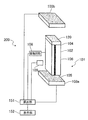
- the optical sensor system 200 includes a light emitting device 102, a reactant 120, two detectors 103a and 103b, a drive circuit 108, a calculation unit 151, and a display unit 152. It consists of and.
- the light emitting device 102, the reactant 120, and the detectors 103a and 103b constitute an optical sensor head 101.
- the optical sensor head 101 is packaged and integrated.
- the light emitting device 102 is provided between the first reflecting surface 104, the second reflecting surface 105 facing the first reflecting surface 104, and the first reflecting surface 104 and the second reflecting surface 105.
- a waveguide 106 is provided.
- the reactant 120 is formed on the first reflecting surface 104.
- the two detectors 103a and 103b are arranged at positions where the light emitting device 102 and the reactant 120 are sandwiched in the direction along the waveguide 106, and the upper surface of the detector 103a faces the second reflecting surface 105 to detect The lower surface of the vessel 103 b faces the upper surface of the reactant 120. As will be described later, only one of the two detectors 103a and 103b may be arranged.
- the drive circuit 108 is connected to the calculation unit 151 and two electrodes (not shown) of the light emitting device 102, and supplies an injection current to the light emitting device 102 through the two electrodes.
- the first reflecting surface 104 and the second reflecting surface 105 are provided at both ends of the waveguide 106, and the space between the first reflecting surface 104 and the second reflecting surface 105 is within the waveguide 106.
- light reciprocates.
- a gain exists in the waveguide 106, and the light traveling back and forth through the waveguide 106 is energy-amplified by the gain, and a part of the light is emitted to the outside from the first reflecting surface 104 and the second reflecting surface 105.
- the light emitting device 102 includes the first reflection surface 104, the second reflection surface 105, and the waveguide 106 to form a resonator.
- a commercially available laser element may be used as the light emitting device 102, and a semiconductor laser element is particularly preferable for miniaturization.
- a distributed feedback laser element may be used.
- the first reflecting surface 104, the second reflecting surface 105, and the waveguide 106 are already provided as long as they are commercially available laser elements (semiconductor laser elements or the like). However, in the optical sensor system 200 according to this embodiment, since the reactant 120 is formed on the first reflecting surface 104, the reflectance of the first reflecting surface 104 is different from that on the market. .
- the detectors 103a and 103b may be small and low-cost commercially available photodetectors.
- the detection surfaces of the detectors 103a and 103b may be slightly inclined with respect to the optical axis so that the light to be detected is reflected and does not return to the light source.
- the detector 103a is arranged immediately after the second reflecting surface 105 of the light emitting device 102 in FIG. 1 and is configured to detect the light intensity of the light transmitted through the second reflecting surface 105. As long as the light intensity of the light transmitted through the second reflection surface 105 can be detected, it may be installed anywhere. Similarly, the detector 103a may be installed anywhere as long as the light intensity of the light transmitted through the first reflecting surface 104 and the reactant 120 can be detected.
- a commercially available semiconductor laser element is provided with a photodetector (photodiode or the like) that monitors the light intensity of the emitted light from the semiconductor laser element.
- this photodetector may be used as the detector 103a. Thereby, the optical sensor system 200 can be easily manufactured.
- the reactant 120 formed on the first reflecting surface 104 of the light emitting device 102 changes its optical properties by changing environmental parameters detected by the optical sensor system 200.
- the optical property include a dielectric constant and a refractive index (including an absorption coefficient).
- the optical property may be one that changes with changes in dielectric constant or refractive index (for example, transmittance, reflectance, absorption, electrical conductivity, or band gap).
- the reactant 120 may be, for example, a thin film or an aggregate of fine particles (for example, metal fine particles that excite surface plasmons), and may have any shape.
- the material of the reactant 120 may be appropriately selected from dielectrics, semiconductors, metals, organic films, and the like according to environmental parameters. For example, since the optical properties of oxides change depending on the amount of oxygen in the surroundings, the reactant formed of the oxide can be used for detecting the concentration of oxidizing or reducing gas or detecting the concentration of oxidizing or reducing liquid. In addition, since the optical properties of a material used for a piezoelectric element or the like change depending on pressure, the pressure applied to the reactant can be detected using the reactant formed of the material. Furthermore, if an organic film that binds only a specific substance is used as a reactant, the concentration of the specific substance can be detected.
- the reactant 120 when the material of the reactant 120 is a metal, it is preferable that the reactant 120 has a shape that can excite surface plasmons. In that case, even if the reactant 120 itself does not react, the surrounding refractive index changes depending on the environmental parameter, so that the excitation condition of the surface plasmon changes, and the reflectance of the first reflecting surface 104 changes. If the light-shielding film (see FIG. 5) is provided with a through-hole as a shape capable of exciting surface plasmons, it is difficult to be influenced by the outside of the through-hole, and information on only the portion provided with the through-hole can be obtained.
- the opening size of the through hole is preferably shorter than the wavelength of the light emitted from the light emitting device 102. In this case, since there is almost no light that passes through the reactant 120, there is almost no influence of the return light. Details of the light shielding film provided with the through hole will be described later.
- the environmental parameters include temperature, humidity, pressure, oxidizing or reducing power, and the type, concentration or quantity of gas, liquid or solid existing around the reactant 120.
- the calculation unit 151 calculates environmental parameters on the first reflecting surface 104 by performing analysis based on the light intensity of the light detected by the detector 103a and / or the detector 103b. Since the analysis may require the driving conditions of the light emitting device 102, the calculation unit 151 is connected to the driving circuit 108 of the light emitting device 102 as shown in FIG.
- the display unit 152 displays the calculation result by the calculation unit 151.
- a commercially available display may be used, and the environmental parameter may be displayed only by numbers.
- a computer is used as the calculation unit 151
- a display corresponding to the computer is used as the display unit 152
- environmental parameters can be displayed in a graph on the display.
- the user can input measurement conditions and analysis contents using an input device such as a keyboard. Note that if the calculation result of the calculation unit 151 is connected to another device, the display unit 152 is not necessary.
- the optical sensor system 200 further includes a temperature sensor 109 disposed in the vicinity of the light emitting device 102.
- a temperature sensor 109 disposed in the vicinity of the light emitting device 102.
- the calculation unit 151 calculates a change in the detection signal of the light emitting device 102 based on the temperature. to correct.
- the calculation unit 151 may be realized by a logic circuit (hardware) formed in an integrated circuit (IC chip) or the like, or may be realized by software using a CPU (Central Processing Unit). In the latter case, the calculation unit 151 includes a CPU that executes instructions of a program that is software for realizing each function. In addition, the calculation unit 151 expands the above program and various data on a ROM (Read Only Memory) or a storage device (referred to as “recording medium”) in which the computer (or CPU) is readable. It further has a RAM (Random Access Memory) and the like. And the function of the calculation part 151 is implement
- a “non-temporary tangible medium” such as a tape, a disk, a card, a semiconductor memory, a programmable logic circuit, or the like can be used.
- the program may be supplied to the computer via an arbitrary transmission medium (such as a communication network or a broadcast wave) that can transmit the program.
- the program can be electronically transmitted in the form of a data signal embedded in a carrier wave.
- a commercially available laser element is used as the light emitting device 102, and the reactant 120 is formed on the first reflecting surface 104.
- commercially available photodetectors are installed at the positions described above as detectors 103a and 103b so that the light intensity of the light emitted to the outside through the second reflecting surface 105 and the first reflecting surface 104 can be detected.
- An external resonator may be added to a commercially available laser element, and the reflection surface thereof may be used as the first reflection surface 104.
- the reactant 120 can be formed on the first reflecting surface 104 of the light emitting device 102 by sputtering, vapor deposition, chemical synthesis, or the like. If the reactant 120 is a conductive material, if the reactant 120 is formed on the entire surface of the first reflective surface 104, the electrode of the light emitting device 102 is short-circuited, so that light is emitted from the first reflective surface 104.
- the reactant 120 may be formed only on the portion to be formed. In that case, the reactant 120 may be formed after masking a part of the first reflecting surface 104.
- the optical sensor head 101 can be manufactured using the existing technology only by forming on the emission surface (first reflection surface 104) of the semiconductor laser element.
- each parameter in the formulas (1) to (3) is as follows.
- ⁇ 1 differential efficiency of light emitted from the first reflecting surface 104
- ⁇ 2 differential efficiency of light emitted from the second reflecting surface 105
- Ith threshold current
- R 1 reflectance of the first reflecting surface 104
- R 2 reflectance of the second reflecting surface 105
- T 1 transmittance of the first reflecting surface 104
- T 2 transmittance of the second reflecting surface 105
- ⁇ stm internal differential efficiency
- ⁇ i internal quantum efficiency
- ⁇ int Internal loss
- J 0 Transparent current
- ⁇ Optical confinement factor of active layer
- h Planck's constant
- ⁇ Light frequency
- q Electron charge
- L Resonator length
- W Active layer width
- d Active layer thickness
- the two detectors 103b and 103a may be used to detect the light intensities of the light emitted from the first reflecting surface 104 and the second reflecting surface 105, respectively. You may detect the light intensity of the light radiated
- the emission intensity P of the semiconductor laser element is the differential efficiency ⁇ 1 of the light emitted from the first reflecting surface 104 or the derivative of the light emitted from the second reflecting surface 105 when the injection current I is greater than or equal to the threshold current Ith. It is known that the efficiency ⁇ 2 is used to express a linear relationship as in the following formula (4).
- FIG. 2 shows differential efficiencies ⁇ 1 of light emitted from the first reflecting surface 104 and the second reflecting surface 105 when the reflectance R 1 of the first reflecting surface 104 in the light emitting device 102 is changed.
- eta 2 is a graph showing changes of the threshold current I th.
- parameters of a typical semiconductor laser element having a wavelength of 785 nm are used. It is assumed that R 2 of the second reflecting surface 105 is fixed at 0.7.
- the differential efficiency ⁇ 1 of the light emitted from the first reflecting surface 104 decreases, and the second reflecting surface 105 It can be seen that the differential efficiency ⁇ 2 of the emitted light increases. Further, as the reflectivity R 1 of the first reflection surface 104 becomes large, it can be seen that the threshold current I th is reduced.
- the light intensity P 1 of the light emitted from the first reflecting surface 104 and the light intensity P 2 of the light emitted from the second reflecting surface 105 when the injection current is 20 mA are calculated.
- the results are shown in FIG.
- the reason why the reflectance R 1 of the first reflecting surface 104 is 0.05 or less and no value is that the threshold current is 20 mA or more in that range, and therefore laser oscillation does not occur when the injection current is 20 mA. .
- the light intensity P 1 of the light emitted from the first reflecting surface 104 than takes the maximum value, the reflectance R 1 is 0.45 when the reflectance R 1 of 0.45 Also decreases as it grows larger. This is because both the threshold current I th and the differential efficiency ⁇ 1 decrease as the reflectance R 1 increases.
- the light intensity P 2 of the light emitted from the second reflecting surface 105 increases monotonously as the reflectance R 1 of the first reflecting surface 104 increases. This is because as the reflectance R 1 increases, the threshold current I th decreases while the differential efficiency ⁇ 2 increases.
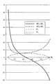
- FIG. 4 shows the reflectance R 1 of the first reflecting surface 104 obtained based on FIG. 3, the light intensity P 1 of the light emitted from the first reflecting surface 104, and the second reflecting surface 105.
- the relationship between the values dP 1 / dR 1 and dP 2 / dR 1 obtained by differentiating the light intensity P 2 of the emitted light by the reflectance R 1 of the first reflecting surface 104 is shown.
- These values dP 1 / dR 1 and dP 2 / dR 1 are the sensitivities of the first reflective surface 104 and the second reflective surface 105 in the optical sensor system 200 according to the present embodiment to the amount of change in the reflectance R 1. It corresponds to.
- a difference in the light intensity detected by the detector 103a and / or the detector 103b with respect to a minute change in the reflectance of the first reflecting surface 104 may be obtained.
- a film having a known refractive index and film thickness
- the surface of the first reflecting surface 104 is formed.
- the reflectance of the first reflecting surface 104 may be measured from the outside using, for example, a commercially available reflectance measuring device.
- the above-described conventional optical sensor system that is, “a system for detecting a change amount of an environmental parameter from reflected light or transmitted light when light is irradiated onto a reactant” will be briefly described.
- the reactant is separated from the light emitting device.
- the reactant 120 is in contact with the first reflecting surface 104 of the light emitting device 102, whereby the change in the optical properties of the reactant 120 is caused by the light emitting device (resonator). ) 102, the light intensity P is not constant, and the light intensity P changes as the reaction of the reactant 120 proceeds.
- the optical property is a reflectance R 1 that changes with a change in refractive index
- the optical sensor system 200 has the sensitivities dP 1 / dR 1 and dP 2 under the condition that the reactants having the same characteristics are irradiated with the light emitted from the light emitting devices having the same characteristics. If the absolute value of / dR 1 is equal to or greater than P (R 1 ) (see the following formula (5)), it is possible to detect the environmental parameter with higher sensitivity than the conventional optical sensor system described above.
- FIG. 4 shows P (R 1 ) and —P (R 1 ) depicted in FIG. 3 together with dP 1 / dR 1 and dP 2 / dR 1 .
- the following equation (5) (5) The range of the reflectance R 1 where is satisfied can be found.
- Parameters related to the equation (5) include reflectance R 1 and R 2 defined by the coating material and film thickness on the reflective surfaces 104 and 105, and the injection current I to the light emitting device 102, and the following: There is.
- ⁇ stm Internal differential efficiency
- ⁇ i Internal quantum efficiency
- ⁇ int Internal loss
- J 0 Transparent current
- ⁇ Optical confinement factor
- L of active layer L Resonator length
- W Active layer width
- d Active layer thickness
- the injection current I can be controlled when the optical sensor system 200 is driven. Therefore, based on measuring the reflectance R 1 with the above-described reflectance measuring device and simultaneously measuring the light intensity P 1 and / or P 2 with the detector 103a and / or the detector 103b, Equation (5) is established.
- the range of the injection current I is calculated in advance from FIG. 4, and the range is stored in the storage unit in the calculation unit 151. Then, when calculating the environmental parameter, an injection current I having a value within the stored range is supplied to the light emitting device 102.
- the drive circuit 108 may be controlled so that the value of the injected current is within an appropriate range.
- the optical sensor system of this embodiment not only has higher sensitivity than the conventional optical sensor system described above, but also requires no optical adjustment because the reactant is formed on the first reflecting surface of the light emitting device. In addition, there is no change over time such as misalignment. Therefore, the number of manufacturing steps is small, and the cost is low because no countermeasure against misalignment is required. Furthermore, when the rising edge of the detection signal of the first detector can be made steep, the detection speed is increased.
- the calculation unit 151 includes the total light amount and the detected light amount of the light emitted from the light emitting device 102.
- the calculated reflectivity or refractive index may be corrected using a correction coefficient determined by the ratio.
- the environmental parameter and the first reflective surface in the first reflective surface 104 are obtained by simulation or actual measurement.
- a set of 104 and the reflectance R 1 is obtained in advance at several points.
- a relational expression between the environmental parameter on the first reflecting surface 104 and the reflectance R 1 on the first reflecting surface 104 is derived, and the calculating unit 151 This relational expression is stored in the storage unit. Based on this relational expression, the calculation unit 151 can calculate an environmental parameter on the first reflecting surface 104 from the reflectance R 1 of the first reflecting surface 104.
- the environmental parameter whose value is known and the light intensity P 1 of the light emitted from the first reflecting surface 104 and / or the light intensity P 2 of the light emitted from the second reflecting surface 105 You may measure the set of several points beforehand.
- the calculation unit 151 can calculate the environmental parameter on the first reflecting surface 104 to be obtained by comparing the light intensity measured for the environmental parameter whose value is unknown with some measured sets.
- the calculation unit 151 includes a storage unit that stores a set of the value of the environmental parameter and the light intensity P 1 and / or P 2 of the light emitted from the light emitting device 102.
- the storage unit may be a commercially available device such as a hard disk, an optical disk, or a solid memory.
- a semiconductor laser element is used as the light emitting device 102.
- the reflectivity of the first reflecting surface 104 changes with changes in the optical properties of the periphery of the reactant 120 or the reactant 120 itself.
- Other laser elements such as a fiber laser may be used as the light emitting device 102 as long as the resonator oscillation conditions change.
- Example 1 In Example 1, the reflectance R 1 of the first reflecting surface 104 before the reaction of the reactant 120 (initial state) in the specific examples described with reference to FIGS. 2 to 4 is 0.3.
- the reflectance R 2 of the second reflecting surface 105 is 0.7, which is higher than the reflectance R 1 of the first reflecting surface 104, and it is difficult to transmit light in the light emitting device 102 to the outside. Therefore, the differential efficiency ⁇ 1 is larger than the differential efficiency ⁇ 2 as shown in FIG. 2, and the light intensity P 1 of the light emitted from the first reflective surface 104 is the second reflective surface 105 as shown in FIG. Is greater than the light intensity P 2 of the light emitted from.
- the light intensity P 2 of the light emitted from the second reflecting surface 105 regardless of the value of reflectance R 1, the increase in reflectivity R 1 of the first reflecting surface 104 It turns out that it increases with it. Therefore, if the reflectance R 1 of the first reflecting surface 104 increases due to the reaction of the reactant 120, the detection intensity at the first detector 103a increases as the reaction of the reactant 120 proceeds, S / N increases. In this case, since the light intensity detected by the detector 103a before the reaction of the reactant 120 can be set to a small value, the driving energy of the light emitting device 102 can be reduced and the power consumption can be reduced.
- the detection intensity at the first detector 103 a decreases as the reaction of the reactant 120 proceeds. Therefore, even if the reaction of the reactant 120 proceeds, the detection intensity of the first detector 103a is not saturated, and the circuit adjustment is performed so that the sensitivity of the detector 103a is maximized in the state before the reaction. it can. Therefore, the S / N can be increased particularly in a region where the amount of change is very small, and highly sensitive detection is possible.
- the light intensity P 1 of the light emitted from the first reflecting surface 104 increases as the reflectance R 1 of the first reflecting surface 104 increases.
- the rate R 1 exceeds 0.45 (maximum value)
- the detection range is preferably a range where R 1 is 0.3 to 0.45.
- Equation (5) does not hold for the light intensity P 1 of the light emitted from the first reflecting surface 104.
- High-sensitivity detection which is the effect of
- R 1 of the first reflecting surface 104 decreases due to the reaction of the reactant 120
- the detection intensity at the first detector 103a decreases as the reaction proceeds. Therefore, the detection intensity of the first detector 103a is not saturated by the reaction, and the circuit can be adjusted so that the sensitivity of the detector 103a is maximized before the reaction. Therefore, the S / N can be increased particularly in a region where the amount of change is very small, and highly sensitive detection is possible.
- Example 2 In Example 2, the reflectance R 1 of the first reflecting surface 104 before the reaction of the reactant 120 (initial state) in the specific example described with reference to FIGS. 2 to 4 is 0.7.
- Example 2 the light intensity P 1 of the light emitted from the first reflecting surface 104 and the light intensity P 2 of the light emitted from the second reflecting surface 105 are both described above. It can be seen that (5) holds. That is, in the case of Example 2, it can be seen that the sensitivity is higher than that of the conventional optical sensor system described above, regardless of whether the light intensity P 1 or the light intensity P 2 is detected.
- the light intensity P 1 of the light emitted from the first reflecting surface 104 is reflected by the first reflecting surface 104 when the reflectance R 1 is in the range of 0.45 to 0.7. It can be seen that the rate R 1 decreases as it increases. Therefore, if the reflectance R 1 of the first reflecting surface 104 increases due to the reaction of the reactant 120, the detection intensity at the second detector 103b decreases as the reaction of the reactant 120 proceeds. Therefore, even if the reaction of the reactant 120 proceeds, the detection intensity of the first detector 103a is not saturated, and the circuit is adjusted so that the sensitivity of the second detector 103b is maximized in the state before the reaction. I can leave.
- the reactant 120 that reflectance R 1 of the first reflection surface 104 is reduced by reacting, as long as the reflectance R 1 is 0.45 or more, first as the reaction of the reactants 120 proceeds
- the detection intensity at the second detector 103b increases, and the S / N increases.
- the driving energy of the light emitting device 102 can be reduced and the power consumption can be reduced.
- the reflectance R 1 of the first reflecting surface 104 increases It can be seen that it increases with time. Therefore, if the reflectance R 1 of the first reflecting surface 104 increases due to the reaction of the reactant 120, the detection intensity at the first detector 103a increases as the reaction of the reactant 120 proceeds, S / N increases. In this case, since the light intensity detected by the detector 103a before the reaction of the reactant 120 can be set to a small value, the driving energy of the light emitting device 102 can be reduced and the power consumption can be reduced.
- the detection intensity at the detector 103 a decreases as the reaction of the reactant 120 proceeds. Therefore, even if the reaction of the reactant 120 proceeds, the detection intensity of the first detector 103a is not saturated, and the circuit is adjusted so that the sensitivity of the first detector 103a is maximized in the state before the reaction. I can leave. Therefore, the S / N can be increased particularly in a region where the amount of change is very small, and highly sensitive detection is possible.
- Example 3 the reflectance R 1 of the first reflecting surface 104 before the reaction of the reactant 120 (initial state) in the specific example described with reference to FIGS. 2 to 4 is 0.45.
- Example 3 the sensitivity dP 1 / dR 1 when detecting the light intensity P 1 of the light emitted from the first reflecting surface 104 is almost 0, and the above equation (5) is established. I understand that there is no. On the other hand, when the light intensity P 2 of the light emitted from the second reflecting surface 105 is detected, the above (5) holds, and it can be seen that the sensitivity dP 2 / dR 1 is higher than the conventional optical sensor system described above. .
- the effect when the reflectance R 1 of the first reflecting surface 104 is increased or decreased by the reaction of the reactant 120 is as described in the first and second embodiments.
- the light intensity P 1 of the light emitted from the first reflecting surface 104 has a maximum value. Therefore, if the reactant 120 has a temperature dependency that the reaction rate is higher as the temperature is higher, the sensitivity is calculated based on the light intensity P 2 while heating at the light intensity P 1. And high sensitivity can be made compatible.
- the reaction of the reactant 120 is reversible, for example, when a reverse reaction (refresh) is performed by light irradiation, refreshing can be performed at the maximum intensity by calculating the sensitivity based on the light intensity P 1. Can be made compatible.
- Example 4 the reflectance R 1 of the first reflecting surface 104 before the reaction of the reactant 120 (initial state) in the specific example described with reference to FIGS. 2 to 4 is 0.1.
- the reflectance R 1 of the first reflecting surface 104 is not defined, and the light intensity P 1 of the light emitted from the first reflecting surface 104 is operated to be constant. Further, at least one of the light intensity P 1 of the light emitted from the first reflecting surface 104 and the light intensity P 2 of the light emitted from the second reflecting surface 105 is more sensitive than the above-described conventional optical sensor system. To be higher.
- the drive circuit 108 which is a control means, performs feedback control based on the light intensity information received via the calculation unit 151 so that the value specified by the user or manufacturer is constant. If the light emitting device 102 is a semiconductor laser element, the driving circuit 108 adjusts the injection current to the element. As shown in FIG. 3, the light intensity P 1 of the light emitted from the first reflecting surface 104 and the light intensity P 2 of the light emitted from the second reflecting surface 105 are the first reflection.
- the drive circuit 108 When the first detector 103a detects only the light intensity P 2 of the light emitted from the second reflecting surface 105 because the dependency of the surface 104 on the reflectance R 1 is different, the calculation unit 151 or the drive Based on the relationship between the light intensity P 1 and the light intensity P 2 stored in the storage unit included in the circuit 108, the drive circuit 108 performs feedback control so that the light intensity P 1 becomes constant.
- the drive circuit 108 may be directly connected to the two detectors 103a and 103b so that the light intensity information can be received without going through the calculation unit 151.
- the amount of change in the light intensity P 2 and / or the light intensity P 1 detected by the detector 103a and / or the detector 103b is recorded in the drive circuit 108 at time intervals for performing feedback control, and sequentially integrated. In this way, since the light intensity P 2 and / or the total change amount of the light intensity P 1 after the reactant 120 starts the reaction can be known, the light when feedback is not applied in the same manner as described above. Based on the calculated intensity, the absolute value of the environmental parameter can be detected.
- the reaction temperature of the reactant 120 is substantially constant. Further, if the reaction of the reactant 120 acts to increase the light intensity P 1 of the light emitted from the first reflecting surface 104, the injection into the light emitting device 102 so as not to increase the light intensity P 1. Since control that gradually decreases the current is performed, power consumption can be reduced.
- Example 6 In Example 6, the reflectance R 1 of the first reflecting surface 104 is not defined, and the light intensity P 1 of the light emitted from the first reflecting surface 104 and the light emitted from the second reflecting surface 105 are reduced. Any of the light intensities P 2 is made more sensitive than the conventional optical sensor system described above.
- the detector 103 a detects the light intensity P 2 of the light emitted from the second reflecting surface 105
- the detector 103 b detects the light intensity P 1 of the light emitted from the first reflecting surface 104.
- the intensity P 1 decreases, and the light intensity P 2 of the light emitted from the second reflecting surface 105 increases.
- the detection intensity at the detector 103b decreases, so that the detection intensity of the second detector 103b does not saturate due to the reaction, and the detector 103b is in a state before the reaction.
- the circuit can be adjusted to maximize the sensitivity. Therefore, the S / N can be increased particularly in a region where the amount of change is very small, and highly sensitive detection is possible.
- the detection intensity at the detector 103a increases as the reaction of the reactant 120 proceeds, and the S / N increases. That is, in the present embodiment, these two effects can be combined.
- the detector 103a and the detector 103b It is preferable to set one of the detectors as high sensitivity and the other as a low sensitivity detector.
- a high-sensitivity detector can increase the detection speed of the optical sensor system 200, and a low-sensitivity detector can widen the measurement range of environmental parameters. That is, a high sensitivity, high speed, and wide range optical sensor system 200 can be obtained.
- the reflectance R 1 of the first reflecting surface 104 has been described with specific values. However, the reflectance R 1 may be set to other values as long as the effects described in the embodiments are obtained. Further, the reflectance R 2 of the second reflecting surface 105 and the value of the injection current may be appropriately changed.
- FIG. 5 is a perspective view of the optical sensor head 1 of the present embodiment.
- the optical sensor head 1 includes a light emitting device 2, a light shielding film 7, a dielectric film 12, and a detector 3. Although not shown, these are packaged and integrated.
- the light emitting device 2 is provided between the first reflecting surface 4, the second reflecting surface 5 facing the first reflecting surface 4, and the first reflecting surface 4 and the second reflecting surface 5.
- a waveguide 6 is provided.
- a light shielding film 7 is formed on the first reflecting surface 4 via a dielectric film 12.
- the light shielding film 7 is provided with a through hole 8 for generating near-field light.
- the hole axis of the through hole 8 is on the extension line of the waveguide 6.
- a first reflecting surface 4 and a second reflecting surface 5 are provided at both ends of the waveguide 6, and light is transmitted between the first reflecting surface 4 and the second reflecting surface 5 in the waveguide 6. Is configured to reciprocate.
- a commercially available laser element may be used as the light emitting device 2, and a semiconductor laser element is particularly preferable for miniaturization.
- a distributed feedback laser element may be used.
- the semiconductor laser element as will be described later, it is easy to calculate the refractive index inside the through hole 8 from the light intensity radiated to the outside through the second reflecting surface 5 detected by the detector 3. It becomes.
- the first reflecting surface 4, the second reflecting surface 5, and the waveguide 6 are already provided as long as they are commercially available laser elements. However, another film can be formed on the first reflecting surface 4 and the second reflecting surface 5 to adjust the reflectance.
- the light shielding film 7 is formed of a material that does not transmit ambient light in order to generate near-field light in the through hole 8.
- the light shielding film 7 is preferably made of a metal that excites surface plasmons. Specifically, materials such as gold, silver, and aluminum are mainly used.
- the through-hole 8 formed in the light shielding film 7 generates near-field light by the light emitted from the light emitting device 2.
- the detection target When the detection target is filled in the through hole 8, the refractive index inside the through hole 8 changes.
- the detection target may be both disposed inside the through-hole 8 alone and disposed in the through-hole 8 in a form contained in gas (for example, air) or liquid (for example, water). .
- the through-hole 8 has a larger area on the light exit surface 7 b of the light shielding film 7 than the opening area on the facing surface 7 a of the light shielding film 7 facing the first reflecting surface 4.
- FIG. 6A is a cross-sectional view showing the xz cross section of the light-shielding film 7 including the one-dot chain line in FIG.
- the increasing rate of the cross-sectional area (xy cross-sectional area) of the through hole 8 is continuous from the facing surface 7a contacting the dielectric film 12 on the first reflecting surface 4 to the light emitting surface 7b. It has become.
- two surfaces facing the x direction among the hole surfaces defining the through hole 8 are tapered surfaces having a constant inclination with respect to the facing surface 7a. Is inclined with respect to the z-axis so that the xy cross-sectional area of the through-hole 8 increases upward, and the rate of increase is constant.
- FIG. 6B which is also a cross-sectional view showing the xz cross-section
- a step-like through hole 28 is formed in the light shielding film 7.
- the increasing rate of the cross-sectional area (xy cross-sectional area) of the through hole 28 is discontinuous from the facing surface 27a that contacts the dielectric film 12 on the first reflecting surface 4 to the light emitting surface 27b.
- FIGS. 6A and 6B illustrate, as an example, a state in which the detection target 9 that is a liquid is filled in the through holes 8 and 28.
- the shape and size of the through holes 8 and 28 strongly influence the intensity distribution of the near-field light in the through holes 8 and 28. Specifically, near-field light tends to be strongly excited as the distance between two surfaces facing each other is shorter.
- the shapes of the through holes 8 and 28 change at least in the xz cross section, thereby opening the through holes 8 and 28 on the emission surfaces 7b and 27b.
- the area is larger than the opening area of the through holes 8 and 28 on the opposing surfaces 7a and 27a.
- the intensity of the near-field light generated in the through holes 8 and 28 is controlled by the opposing surface regardless of whether the linearly polarized light, the circularly polarized light or the elliptically polarized light is emitted from the light emitting device 2 and the direction of the polarized light. In the vicinity of 7a and 27a, it can be made stronger than in the vicinity of the exit surfaces 7b and 27b.
- the shapes of the through holes 8 and 28 may be changed in both the xz cross section and the yz cross section.
- near-field light generated in the through-holes 8 and 28 is concentrated in the vicinity of the opposing surfaces 7a and 27a of the light-shielding film 7, so that it is farther from the through-holes 8 and 28 when measuring the refractive index inside the through-holes 8 and 28. It is almost unaffected by the refractive index. Therefore, the refractive index in the vicinity of the through holes 8, 28, mainly the inside of the through holes 8, 28 can be detected with high sensitivity. For this reason, if the opening area in the opposing surfaces 7a and 27a of the through-holes 8 and 28 is sufficiently small, detection at the molecular level can be performed. Further, since the detection target only needs to exist inside the through holes 8 and 28, the sample volume can be reduced. Furthermore, since a separate light source is not required, the size can be reduced.
- the cross-sectional shape of the through hole 8 may be not a straight line (trapezoid) but a curved line (a bowl). Further, as long as the rate of increase in the cross-sectional area of the through hole is continuous, the inclination angle may change midway. Further, the cross-sectional shape of the through-hole 28 is not a two-stage change as shown in FIG. 6B, but a multi-stage change of three or more stages as long as the increase rate of the cross-sectional area of the through-hole is discontinuous. However, it may not have a horizontal part and / or a vertical part.
- the through holes 8 and 28 may be asymmetrical rather than symmetrical with respect to the z axis (FIGS. 6A and 6B).
- one side may be a surface parallel to the z-axis.
- the detection target hardly stays in the vicinity of the light emission surface 7b, and can smoothly enter the vicinity of the opposing surface 7a where the light intensity distribution is strong. For this reason, even if the area of the opposing surface 7a is small, it can be detected with sufficient sensitivity.
- the range in which the light intensity distribution inside the through hole 28 is strong can be widened, and the detection sensitivity can be increased.
- the through hole is formed so that the opening area of the through hole on the emission surface is larger than the opening area of the through hole on the opposing surface. It is sufficient that the shape is changed at least in either or both of the xz cross section and the yz cross section. If the light emitted from the light emitting device 2 includes both x-polarized light and y-polarized light, the opening area of the through hole on the emission surface is larger than the opening area of the through hole on the opposing surface.
- the shape of the through hole only needs to change in at least one of the xz cross section and the yz cross section. In this case, it is preferable that the shape of the through hole is changed in both the xz cross section and the yz cross section.
- surface plasmons have a property of being strongly excited on a plane orthogonal to the polarization direction of incident light. Therefore, in this embodiment, if the light emitted from the light emitting device 2 is x-polarized light, the shape of the through-holes 8 and 28 changes at least in the xz cross section, thereby relating to the x direction on the emission surfaces 7b and 27b.
- the opening lengths of the through holes 8 and 28 are larger than the opening lengths of the through holes 8 and 28 in the x direction on the facing surfaces 7a and 27a. Thereby, the intensity of the near-field light generated in the through holes 8 and 28 can be made stronger near the opposing surfaces 7a and 27a than near the exit surfaces 7b and 27b. Therefore, the detection sensitivity can be further increased.
- the opening length of the through holes 8 and 28 in either the x direction or the y direction on the facing surfaces 7a and 27a is smaller than the wavelength of the light emitted from the light emitting device 2. Thereby, there is almost no light transmitted through the through holes 8 and 28, and it is difficult to be influenced by the outside of the through holes 8 and 28, and only the refractive index change inside the through holes 8 and 28 can be detected.
- the opening size of the through holes 8 and 28 can be set to about several nanometers, it is possible to allow only one molecule to be detected to enter the through holes 8 and 28. That is, the through holes 8 and 28 can also have a function of selecting a detection target having a certain size or less.
- the optimal through-hole with which the near-field light intensity to be generated has a very narrow shape, if the discontinuous shape as shown in FIG.
- the detection target that can enter the inside of the through hole 28 can be selected based on the opening size of the through hole 28 in 27b.
- the detector 3 may be a commercially available photodetector or a spectroscope. Commercially available photodetectors can only detect intensity, but are small and low cost. On the other hand, although the spectroscope cannot be made so small, it can detect not only the intensity but also wavelength shift information because it can detect the reflection spectrum.
- a detector may be disposed on the opposite side of the light emitting device 2 with the light shielding film 7 interposed therebetween. In that case, the detector detects the light intensity of the light passing through the first reflecting surface 4 and the through hole 8. The light passing through the through hole 8 is light in which near-field light generated mainly in the through holes 8 and 28 is scattered.
- the near-field light generated in the through-holes 8 and 28 is stronger in the vicinity of the opposing surfaces 7a and 27a than in the vicinity of the exit surfaces 7b and 27b. Therefore, the intensity of light scattered from the near-field light in the vicinity of the opposing surfaces 7a and 27a. Become stronger. Therefore, even when light passing through the through hole 8 is detected, it is difficult to be influenced by the outside of the through holes 8 and 28, and only the refractive index change inside the through holes 8 and 28 can be detected.
- the refractive index inside the through-holes 8 and 28 changes, the first reflecting surface 4 (which will be described below assuming that the dielectric film 12 is not provided, but when the dielectric film 12 is provided).
- the same reflectance as described below holds, and the light intensity distribution in the waveguide 6 reciprocating between the first reflecting surface 4 and the second reflecting surface 5 changes.
- the transmittance of light emitted from the second reflecting surface 5 changes. Therefore, the refractive index inside the through holes 8 and 28 can be determined by detecting the transmittance of the light emitted from the second reflecting surface 5. For example, if an adsorption layer for adsorbing specific molecules is provided in the through holes 8 and 28, the concentration of the specific molecules can be known.
- the light intensity distribution was obtained by FDTD simulation for the following three structures (1), (2), and (3).
- the light-shielding film 7 is gold having a thickness of 135 nm
- the through-hole 8 has a width in the xz direction on the first reflecting surface 4 of 50 nm, and a width in the xz direction on the light emission surface is 200 nm.
- the light shielding film 7 has a thickness of 135 nm of gold
- the light-shielding film 7 is gold having a thickness of 135 nm
- the through-hole 8 is a slit having a width of 50 nm in the xz direction, and continues infinitely in the y direction.
- the incident light was all polarized in the width direction (x direction) of the slit and had a wavelength of 780 nm.
- FIGS. 7 (a), (b), and (c) are the simulation results of the light intensity distribution in the cross section including the polarization direction for the structures (1), (2), and (3), respectively. the same).
- the through hole is a conventional simple slit shape (structure (3))
- the strength is highest at the edge of the through hole on the light exit surface as shown in FIG. Therefore, strong light is distributed outside the light exit surface.
- the highest strength in the structure (1) is the edge of the through hole 8 in the opposing surface 7a
- the highest strength in the structure (2) is from the opposing surface 27a until the slit width changes. is there. That is, in the structures (1) and (2), the light intensity distribution can be brought closer to the inner side than the light exit surfaces 7b and 27b, and the structure is sensitive to the refractive index change inside the through holes 8 and 28. ing.
- the structure (2) has a wider range of strong light intensity inside the through hole, and the detection sensitivity can be increased.
- the structure (1) is less affected by the outside of the through hole.
- the detection target is less likely to stay near the light exit surface 7b, and the detection target can smoothly enter the vicinity of the opposing surface 7a where the light intensity is high.
- FIGS. 7D, 7E, and 7F are simulation results of light intensity distribution in cross sections including the width direction of the slits for the structures (1), (2), and (3), respectively. However, these have an intensity scale of 1/3 with respect to FIGS. 7 (a), (b), and (c). If the through hole is a conventional simple slit shape (structure (3)), as shown in FIG. 7 (f), the light just oozes around the through hole 8 on the facing surface 7a.
- the amount of oozing increases and the intensity distribution of light inside the light exit surfaces 7b and 27b can be enhanced.
- the intensity distribution from the facing surfaces 7a and 27a toward the exit surfaces 7b and 27b in the hole axis is shown in FIG. From this graph, it can be seen that the light intensity inside the through holes of the structures (1) and (2) is stronger than that of the structure (3), and the intensity at the exit surfaces 7b and 27b is sufficiently low. That is, the structures (1) and (2) are sensitive to changes in the refractive index inside the through holes 8 and 28.
- the oscillation conditions of the semiconductor laser element are threshold current and differential efficiency. These are generally known to be expressed by the following mathematical formulas (1) to (3).
- each parameter is as follows.
- ⁇ 1 differential efficiency of light emitted from the first reflecting surface 4
- ⁇ 2 differential efficiency of light emitted from the second reflecting surface 5
- I th threshold current
- R 1 reflection of the first reflecting surface 4
- R 2 reflectivity of the second reflecting surface 5
- T 1 transmittance of the first reflecting surface 4
- T 2 transmittance of the second reflecting surface 5
- ⁇ stm internal differential efficiency
- ⁇ i internal quantum efficiency
- ⁇ int internal loss
- J 0 transparency current
- ⁇ optical confinement factor of active layer h: Planck constant
- ⁇ frequency of light
- L resonator length
- W active layer width
- d active layer thickness
- FIG. 8A shows that the differential efficiency ( ⁇ 2 ) of the light emitted from the second reflecting surface 5 changes as the reflectance (R 1 ) of the first reflecting surface 4 changes. .
- the differential efficiency of light emitted from the second reflecting surface 5 with respect to the change in the reflectance (R 1 ) of the first reflecting surface 4 It can be seen that the amount of change in ⁇ 2 ) increases.
- the reflectance (R 2 ) of the second reflecting surface 5 is smaller, the differential efficiency of the light emitted from the second reflecting surface 5 with respect to the change in the reflectance (R 1 ) of the first reflecting surface 4 ( It can be seen that the amount of change in ⁇ 2 ) increases.
- the reflectance (R 1 ) of the first reflecting surface 4 is large, and the second It is preferable that the reflectance (R 2 ) of the reflecting surface 5 is small.
- FIG. 8B shows that the threshold current changes as the reflectance (R 1 ) of the first reflecting surface 4 changes. It can also be seen that the smaller the reflectance (R 1 ) of the first reflecting surface 4 is, the larger the amount of change in the threshold current with respect to the change in the reflectance (R 1 ) of the first reflecting surface 4 is. However, even if the reflectance (R 2 ) of the second reflecting surface 5 changes, the amount of change in the threshold current with respect to the change in the reflectance (R 1 ) of the first reflecting surface 4 hardly changes. That is, as the reflectance (R 2 ) of the second reflecting surface 5 is smaller, the threshold current value is larger, but the overall curve is substantially the same, and the amount of change in the threshold current is almost unchanged.
- the reflectance (R 1 ) of the first reflecting surface 4 is small.
- the amount of light emitted from the first reflecting surface 4 becomes strong or the amount of light absorbed by the first reflecting surface 4 is large.
- heat is applied to the detection target 9 existing in the vicinity of the first reflecting surface 4. For this reason, it is preferable to correct the temperature change due to the amount of heat.
- the light-emitting device 2 may be a commercially available laser element. If the light-shielding film 7 is formed on the first reflective surface 4 via the dielectric film 12 and then the through-hole 8 is formed in the light-shielding film 7. Good. Then, a commercially available photodetector may be installed as the detector 3 so that the light intensity of light emitted outside through the second reflecting surface 5 can be detected.
- a semiconductor laser element when used as the light emitting device 2, a type in which the semiconductor laser element and the detector 3 for monitoring the emission intensity from the back surface of the semiconductor laser element are packaged can be used.
- a light-shielding film 7 gold, silver, aluminum, etc.
- a film is formed by vapor deposition or the like, and then the through hole 8 may be formed by FIB (Focused Ion Beam) or photolithography.
- the FIB focused beam scanning method and photolithography conditions are appropriately set. Just decide. For example, in order to make a structure as shown in FIG. 6A, the number of scans in the FIB in the x direction may be reduced toward the outside and the number of scans in the center may be increased. Alternatively, a mask may be set in advance in the region of the through hole 8 and the light shielding portion may be formed by forming the film from an oblique direction, and then the mask of the through hole 8 may be removed. In order to make a structure as shown in FIG. 6B, a wide concave portion is dug in the light emission surface 27b, and then a narrow through hole is formed between the bottom surface of the concave portion and the opposing surface 27a. Just dig in.
- the light-emitting device 2 When the light-emitting device 2 is used in a gas, sensing can be performed with only the above-described configuration. However, when more precise measurement is performed or when the light-emitting device 2 is used in a liquid, a device is required. In particular, when the light-emitting device 2 is a semiconductor laser element, if the optical sensor head 1 is brought into contact with the liquid as it is, the p-electrode and the n-electrode are brought into conduction, so that the light is not emitted and is destroyed in the worst case.
- FIG. 9 is a perspective view illustrating an example of the flow path member 10.
- a window (opening) 11 that exposes the flow path to the outside is provided at the center of the upper surface of the flow path member 10 in which a flow path from left to right is formed inside.
- the window 11 is preferably formed to be larger than the opening size in the exit surface 7 b of the through hole 8.
- the flow path member 10 is brought into close contact with the light shielding film 7 so that the through hole 8 of the light shielding film 7 is within the range of the window 11 (preferably coincident with the opening on the emission surface 7b) (see FIG. 11).
- a gas or liquid including the detection target 9 is leaked by sandwiching a rubber ring between the light shielding film 7 and the flow path member 10 so as to surround the opening and the window 11 in the emission surface 7b of the through hole 8. Can be washed away.
- the width of the flow path member 10 is narrow around the window 11, but the width of the flow path member 10 may be uniform.
- the end of the flow path member 10 may be connected to a tube or the like so that the liquid containing the detection target 9 can be sucked out of the flow path member 10.
- the window 11 may be smaller than the opening size of the exit surface 7 b of the through hole 8, but depending on the flow velocity of the gas and / or liquid including the detection target 9, the detection target 9 is within the range of the through hole 8 larger than the window 11. There is a risk of accumulation of gas and / or liquid containing.
- a recess 41 connected to the through hole 8 is formed in the dielectric film 22 formed on the first reflecting surface 4.
- the recess 41 is defined by a tapered surface that has the same inclination angle as that of the above-described tapered surface that defines the through-hole 8 and is connected to the inclined surface to form one inclined surface.
- the through-hole 8 and the recessed part 41 together form one recessed part.
- the size of the through hole 8 in the x direction is the smallest at the bottom surface of the recess 41, and thus the light intensity is the strongest here.
- the recessed part 41 connected to the through-hole 8 is formed in the dielectric film 22, since the detection target 9 can exist also in the recessed part 41, a sensitivity can be raised further.
- a recess 42 connected to the through hole 28 is formed in the dielectric film 32 formed on the first reflecting surface 4.
- the recess 42 is defined by two vertical surfaces separated by the same width as the lower vertical portion below the horizontal portion of the through hole 28.
- the through hole 28 and the recess 42 are combined to form one recess.
- the size of the through hole 28 in the x direction is the smallest between the horizontal portion and the bottom surface of the recess 42, and the light intensity is the strongest here. If the concave portion 42 connected to the through hole 28 is formed in the dielectric film 32 as described above, the detection target 9 can exist also in the concave portion 42, so that the sensitivity can be increased.
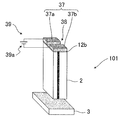
- the optical sensor head 101 shown in FIG. 11 uses a light shielding film 37 divided into two regions 37a and 37b that are insulated from each other with the through hole 38 as a boundary.
- the through hole 38 is formed as a slit that divides the light shielding film 37 into two, but this is not necessarily the case, and the light shielding film is insulated from each other by the through hole and the insulating layer. It may be divided into two regions.
- a circuit 39 including a DC power supply 39a is provided as a voltage applying means for applying a DC voltage between the two regions 37a and 37b of the light shielding film 37.
- the detection target can be collected in the through hole 38 by electrophoresis. This is because when a voltage is applied between the two regions 37a and 37b that are insulated from each other, a strong electric field is generated at a place where the distance between the two regions 37a and 37b is the narrowest.
- the detection sensitivity is further improved. Note that an AC voltage may be applied between the two regions 37a and 37b, and the size of the detection target that can be collected may be selected based on the frequency.
- FIG. 12 analyzes the result detected by the optical sensor head 1 shown in detail in FIG. 5 and the detector 3 of the optical sensor head 1, and calculates the refractive index in the through hole 8. 51, a display unit 52 that displays the calculation result of the calculation unit 51, and a drive circuit 53.
- the calculation unit 51 may be a circuit system alone, or may be a computer and software that operates on the computer.
- the display unit 52 may be a commercially available display, and may display only numbers (refractive index).
- a computer is used as the calculation unit 51, if a display corresponding to the computer is used as the display unit 52, the refractive index can be displayed in a graph on the display.
- the user can input measurement conditions and analysis contents using an input device such as a keyboard.
- the drive circuit 53 is a circuit for driving the light emitting device 2 of the optical sensor head 1, and is connected to two electrodes (not shown) of the light emitting device 2, and an injection current is injected into the light emitting device 2 through the two electrodes. Supply. Since the analysis in the calculation unit 51 may require the driving condition of the light emitting device 2, the calculation unit 51 is connected to the driving circuit 53 of the light emitting device 2 as shown in FIG.
- the program provided with an algorithm related to the operation of the optical sensor system described later may be provided by the manufacturer or may be created by the user.
- the differential efficiency ( ⁇ 2 ) of the light emitted from the second reflecting surface 5 a current is passed through the light emitting device 2 at at least two current values equal to or higher than the threshold current, The light intensity of the light emitted from the second reflecting surface 5 is detected by the detector 3.
- the calculation unit 51 obtains the differential efficiency ( ⁇ 2 ) by dividing the difference between the plurality of detection intensities detected by the detector 3 by the difference in current value.
- the detector 3 When the detector 3 is configured to detect only a part of the light emitted from the second reflecting surface 5, the total light amount and the detected light amount of the light emitted from the second reflecting surface 5 are determined.
- the calculation of the refractive index may be corrected by the ratio. In that case, the memory
- the detector 3 detects the light intensity of the light radiated from the second reflecting surface 5 at that time by passing the current with at least two current values equal to or greater than the threshold current. To do. After calculating the differential efficiency ( ⁇ 2 ) of the light emitted from the second reflecting surface 5 by the calculation unit 51, the light intensity at a certain current value and the calculated differential efficiency ⁇ 2 are substituted into Equation (6). By doing so, a threshold current is obtained.
- the relationship between the refractive index inside the through-hole 8 and the reflectance of the first reflecting surface 4 is calculated in advance by FDTD simulation. Or some points are calculated
- the calculation unit 51 only needs to have a storage unit that stores the result of measuring a sample whose concentration is known before measurement.
- the storage unit may be a commercially available device such as a hard disk, an optical disk, or a solid memory.
- the oscillation wavelength of a semiconductor laser element changes depending on the environmental temperature. Based on this principle, if a spectroscope is used as the detector 3 to measure not only the intensity but also the spectrum, changes in the threshold current and the differential efficiency due to changes in the environmental temperature can be corrected. Also, the refractive index can be corrected by the temperature of the detection target and the light shielding film. Specifically, the calculation unit 51 may hold the result of measuring the relationship between the temperature and the oscillation wavelength in advance, or may be calculated from the configuration of the semiconductor laser element.
- a plurality of optical sensor heads 1 may be used.
- the shape of the through hole 8, the material of the light shielding film 7, the wavelength of the light emitting device 2 are different from each other, information obtained from each optical sensor head 1 is different.
- the optical sensor heads 1 may be arranged apart from each other, may be arranged close to each other, and may be selected depending on the purpose.
- the information obtained from the plurality of optical sensor heads 1 is integrated and the time change or location of the detection target 9 is determined. You can also get dependency information. Furthermore, if the temperature of the detection target 9 or the flow velocity of the detection target 9 is changed and the change in time or location is measured, the dynamic characteristics (viscosity, dispersion, etc.) of the detection target 9 in the flow path can be known. . If an adsorption layer that adsorbs specific molecules is provided inside the through-hole 8 and the concentration of the specific molecules is detected, the reaction conditions (reaction rate, dissociation constant, etc.) for the adsorption layer can be known.
- the optical sensor system according to Embodiment 1 described above includes a first reflecting surface, a second reflecting surface facing the first reflecting surface, and the first reflecting surface and the second reflecting surface.
- a light emitting device having a waveguide provided therebetween, a reactant formed on the first reflecting surface, and light emitted from one of the first reflecting surface and the second reflecting surface
- an optical sensor system comprising: a first detector that detects an intensity; and a calculator that calculates an environmental parameter on the first reflecting surface based on the light intensity detected by the first detector.
- the reflectance R 1 of the first reflecting surface and the light intensity P (R 1 ) detected by the detector are: Satisfy the relationship.
- the optical sensor system is more sensitive than the above-described conventional optical sensor system.
- the reactant is formed on the first reflecting surface of the light emitting device, optical adjustment is not required and a change with time such as a positional shift does not occur. Therefore, the number of manufacturing steps is small, and the cost is low because no countermeasure against misalignment is required. Furthermore, when the rising edge of the detection signal of the first detector can be made steep, the detection speed is increased.
- the reactant R reacts to increase the reflectance R 1 of the first reflecting surface, or The reflectance R 1 of the first reflecting surface is reduced by the reaction of the reactants.
- the reactant reacts, the light intensity of the light detected by the first detector increases, so the S / N increases. Further, since the light intensity detected by the detector before the reaction can be set to a small value, the driving energy of the light emitting device can be reduced and the power consumption can be reduced.
- the material and film thickness of the reactant may be appropriately selected according to the coating state of the first reflecting surface.
- the reflectance R 1 of the first reflecting surface is reduced by the reaction of the reactant, or And the reactant R reacts to increase the reflectance R 1 of the first reflecting surface.
- the optical sensor system described above further includes control means for performing feedback control based on the light intensity detected by the first detector so that the light intensity detected by the first detector is constant. I have. With the above configuration, since the light intensity irradiated to the reactant is constant, the reaction temperature of the reactant is substantially constant. If the reaction of the reactant acts to increase the light intensity of the light emitted from the first reflecting surface, the injection current to the light emitting device is gradually decreased so as not to increase the light intensity. Therefore, power consumption can be reduced.
- the optical sensor system described above further includes a second detector that detects the light intensity of light emitted from the other of the first reflecting surface and the second reflecting surface.
- the detection speed of the optical sensor system can be increased with a high sensitivity detector, and the environmental parameter of a low sensitivity detector can be increased.
- the measurement range can be widened. That is, a high sensitivity, high speed, and a wide range of optical sensor systems can be obtained.
- the optical sensor head includes a first reflection surface, a second reflection surface facing the first reflection surface, and the first reflection surface and the second reflection surface.
- a light-emitting device having a waveguide provided therebetween, a light-shielding film formed on the first reflecting surface, having a through-hole for generating near-field light, and the first or first
- a detector for detecting the light intensity of light emitted from the light emitting device through the two reflecting surfaces, wherein the opening area of the through hole on the light emitting surface of the light shielding film is The opening area of the through hole on the opposing surface of the light shielding film opposite to the first reflecting surface is larger.
- the light intensity distribution in the through hole is weak near the light exit surface and strong near the opposing surface, it is not easily affected by the outside of the through hole, and only the refractive index change inside the through hole is good. Can be detected with sensitivity. For this reason, if the opening size on the opposing surface of the through hole is made sufficiently small, detection at the molecular level can be performed. In addition, since only the detection target that can enter into the opening on the opposing surface of the through hole is detected, it is possible to detect the detection target after selecting it according to the opening size. Furthermore, since the detection target only needs to exist inside the through hole, the sample volume can be reduced. Further, since a separate light source is not required, the size can be reduced.
- the light shielding film is made of a material that excites surface plasmons. According to the said structure, since the material of a light shielding film is a material which excites surface plasmon, the intensity
- the light emitted from the light emitting device is linearly polarized light
- the opening length of the through hole on the light exiting surface of the light shielding film with respect to the direction of the linearly polarized light is on the opposing surface of the light shielding film. It is larger than the opening length of the through hole.
- the light emitted from the light emitting device is linearly polarized light, and the opening length of the through hole in the direction of the linearly polarized light on the facing surface of the light shielding film is greater than the wavelength of light emitted from the light emitting device. small. According to the said structure, there is almost no light which permeate
- the increase rate of the cross-sectional area of the through hole is continuous. According to the above configuration, the detection target hardly stays in the vicinity of the light emission surface, and can smoothly enter the opposite surface side where the light intensity distribution is strong. For this reason, even if the area on the facing surface is small, it can be detected with sufficient sensitivity.
- the increase rate of the cross-sectional area of the through hole is discontinuous. According to the said structure, the range where the intensity distribution of the light inside a through-hole is strong becomes wide, and it can raise detection sensitivity.
- a dielectric film formed between the light emitting device and the light shielding film is further provided, and the dielectric film has a recess connected to the through hole. According to the above configuration, since the detection target can exist also in the recess formed in the dielectric film, the sensitivity can be further increased.
- the light emitting device is a semiconductor laser element. According to the above configuration, a small optical sensor head can be obtained, and the refractive index inside the through hole can be calculated from the light intensity radiated to the outside through the first or second reflecting surface detected by the detector. Easy.
- the detector is a spectroscope capable of measuring spectrum, and detects the wavelength of light emitted to the outside through the first or second reflecting surface. According to the above configuration, since the oscillation temperature of the semiconductor laser depends on the ambient temperature, the ambient temperature can be calculated from the detected wavelength, and the calculation of the refractive index can be corrected. Detection is possible.
- the light shielding film is divided into two regions insulated from each other with the through hole as a boundary, Voltage application means for applying a voltage between the two regions of the light shielding film is further provided.
- a detection target can be collected inside a through-hole by applying a voltage between the said 2 area
- the optical sensor system is calculated by the optical sensor head, a calculation unit that calculates a refractive index in the through hole based on a detection value of the detector when the light emitting device emits light, and a calculation unit that calculates And a display unit for displaying the refractive index.
- it becomes an optical sensor system which is hard to receive the influence outside a through-hole, can detect only the refractive index change inside a through-hole, and can also detect a molecular level.
Landscapes
- Chemical & Material Sciences (AREA)
- Physics & Mathematics (AREA)
- Health & Medical Sciences (AREA)
- General Health & Medical Sciences (AREA)
- Life Sciences & Earth Sciences (AREA)
- Analytical Chemistry (AREA)
- Biochemistry (AREA)
- General Physics & Mathematics (AREA)
- Immunology (AREA)
- Pathology (AREA)
- Plasma & Fusion (AREA)
- Chemical Kinetics & Catalysis (AREA)
- Engineering & Computer Science (AREA)
- Nuclear Medicine, Radiotherapy & Molecular Imaging (AREA)
- Investigating Or Analysing Materials By Optical Means (AREA)
Abstract
Description

本発明の実施形態1に係る光学センサシステム及びその実施例について、図1~図4を参照して説明する。
本実施形態に係る光学センサシステム200は、図1に示すように、発光デバイス102と、反応体120と、2つの検出器103a、103bと、駆動回路108と、算出部151と、表示部152とから構成されている。発光デバイス102、反応体120、及び、検出器103a、103bが光学センサヘッド101を構成している。図示を省略しているが、光学センサヘッド101はパッケージ化されて一体となっている。発光デバイス102は、第1の反射面104、第1の反射面104と対向する第2の反射面105、および、第1の反射面104と第2の反射面105との間に設けられた導波路106を有している。反応体120は、第1の反射面104上に形成されている。2つの検出器103a、103bは、発光デバイス102及び反応体120を導波路106に沿った方向に挟む位置に配置されており、検出器103aの上面が第2の反射面105と対向し、検出器103bの下面が反応体120の上面と対向している。なお、後述するように、2つの検出器103a、103bのうちのどちらか一方だけが配置されていてもよい。駆動回路108は、算出部151と、発光デバイス102の図示しない2つの電極とに接続されており、当該2つの電極を介して発光デバイス102に注入電流を供給する。
算出部151は、集積回路(ICチップ)等に形成された論理回路(ハードウェア)によって実現してもよいし、CPU(Central Processing Unit)を用いてソフトウェアによって実現してもよい。後者の場合、算出部151は、各機能を実現するソフトウェアであるプログラムの命令を実行するCPUを有している。また、算出部151は、上記プログラムおよび各種データがコンピュータ(またはCPU)で読み取り可能に記録されたROM(Read Only Memory)または記憶装置(これらを「記録媒体」と称する)、上記プログラムを展開するRAM(Random Access Memory)などをさらに有している。そして、コンピュータ(またはCPU)が上記プログラムを上記記録媒体から読み取って実行することにより、算出部151の機能が実現される。
次に、図1に示す光学センサヘッド101の製造方法の一例を説明する。発光デバイス102として市販のレーザ素子を用い、その第1の反射面104に反応体120を形成する。次に、第2の反射面105及び第1の反射面104を通して外部に出射される光の光強度をそれぞれ検出できるように、市販のフォトディテクタを検出器103a、103bとしてそれぞれ上述した位置に設置する。なお、市販のレーザ素子に外部共振器を加え、その反射面を第1の反射面104としてもよい。
次に、算出部151で行なわれる、検出器103a及び/又は検出器103bで検出された光の光強度に基づいた解析、および環境パラメータの算出原理について説明する。なお、以下の説明においては、発光デバイス102が半導体レーザ素子であるとする。
上述のとおり、環境パラメータの変化により、反応体120の周辺または反応体120自体の光学的性質が変化し、第1の反射面104の反射率が変化する。まず、この第1の反射面104の反射率の変化が、発光デバイス102である半導体レーザ素子の発光強度に与える影響の計算について説明する。
η1:第1の反射面104から放射された光の微分効率
η2:第2の反射面105から放射された光の微分効率
Ith:閾値電流
R1:第1の反射面104の反射率
R2:第2の反射面105の反射率
T1:第1の反射面104の透過率
T2:第2の反射面105の透過率
ηstm:内部微分効率
ηi:内部量子効率
αint:内部損失
J0:透明化電流
Γ:活性層の光閉じ込め係数
h:プランク定数
ν:光の振動数
q:電子の電荷
L:共振器長
W:活性層の幅
d:活性層厚さ
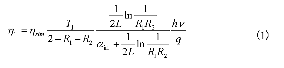
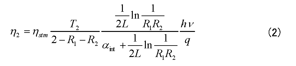

P1=η1(I-Ith)
P2=η2(I-Ith) (4)
反射の場合には、d(P0R1)/dR1=P0と、
透過の場合には、d{P0(1-R1)}/dR1=-P0
と表される。

が成り立つ反射率R1の範囲がわかる。
ηstm:内部微分効率
ηi:内部量子効率
αint:内部損失
J0:透明化電流
Γ:活性層の光閉じ込め係数
L:共振器長
W:活性層の幅
d:活性層厚さ
λ:発光デバイス102が出射する光の波長
続いて、本実施形態の光学センサシステム200における幾つかの実施例について説明する。
実施例1は、図2~図4で説明した具体例において、反応体120が反応する前(初期状態)の第1の反射面104の反射率R1を0.3としたものである。
実施例2は、図2~図4で説明した具体例において、反応体120が反応する前(初期状態)の第1の反射面104の反射率R1を0.7としたものである。
実施例3は、図2~図4で説明した具体例において、反応体120が反応する前(初期状態)の第1の反射面104の反射率R1を0.45としたものである。
実施例4は、図2~図4で説明した具体例において、反応体120が反応する前(初期状態)の第1の反射面104の反射率R1を0.1としたものである。
実施例5では、第1の反射面104の反射率R1を規定せず、第1の反射面104から放射された光の光強度P1が一定になるように動作させる。また、第1の反射面104から放射された光の光強度P1および第2の反射面105から放射された光の光強度P2の少なくともいずれかが、上述した従来の光学センサシステムより感度が高くなるようにする。本実施例では、検出器103a及び/又は検出器103bを用いて光強度P2及び/又は光強度P1を検出するとともに、第1の反射面104から放射された光の光強度P1がユーザまたはメーカーにより規定された値で一定となるよう、制御手段である駆動回路108が算出部151を介して受け取った光強度情報に基づいたフィードバック制御を行う。発光デバイス102が半導体レーザ素子であれば、駆動回路108が当該素子への注入電流を調整することになる。図3に示されているように、第1の反射面104から放射された光の光強度P1と第2の反射面105から放射された光の光強度P2とでは、第1の反射面104の反射率R1への依存性が異なるため、第1の検出器103aが第2の反射面105から放射された光の光強度P2のみが検出される場合、算出部151または駆動回路108に含まれる記憶部に記憶された光強度P1と光強度P2との関係に基づいて、光強度P1が一定となるように駆動回路108がフィードバック制御を行う。なお、変形例として、算出部151を介することなく光強度情報を受け取ることができるように、駆動回路108が2つの検出器103a、103bと直接接続されていてもよい。
実施例6では、第1の反射面104の反射率R1を規定せず、第1の反射面104から放射された光の光強度P1および第2の反射面105から放射された光の光強度P2のいずれも、上述した従来の光学センサシステムより感度が高くなるようにする。
次に、貫通孔8が設けられた遮光膜7が反応体120である、本発明の実施形態2に係る光学センサヘッド1について図5~図8を参照して説明する。
図5は、本実施形態の光学センサヘッド1の斜視図である。光学センサヘッド1は、発光デバイス2と遮光膜7と誘電体膜12と検出器3とから構成されている。図示を省略しているが、これらはパッケージ化されて一体となっている。発光デバイス2は、第1の反射面4、第1の反射面4と対向する第2の反射面5、および、第1の反射面4と第2の反射面5との間に設けられた導波路6を有している。第1の反射面4上には誘電体膜12を介して遮光膜7が形成されている。遮光膜7には、近接場光を発生させるための貫通孔8が設けられている。貫通孔8の孔軸は導波路6の延長線上にある。
貫通孔8,28内部の屈折率が変化すると、第1の反射面4(以下では誘電体膜12が設けられていないと仮定して説明するが、誘電体膜12が設けられている場合にも以下と同様の説明が成り立つ)の反射率が変化し、第1の反射面4および第2の反射面5間を往復する導波路6中の光の強度分布が変化する。そのため、第2の反射面5から出射される光の透過率が変化する。よって、第2の反射面5から出射される光の透過率を検出することで、貫通孔8,28内部の屈折率がわかる。例えば、貫通孔8,28内部に、特定の分子を吸着する吸着層を設けておけば、この特定の分子の濃度がわかる。



η1:第1の反射面4から放射された光の微分効率
η2:第2の反射面5から放射された光の微分効率
Ith:閾値電流
R1:第1の反射面4の反射率
R2:第2の反射面5の反射率
T1:第1の反射面4の透過率
T2:第2の反射面5の透過率
ηstm:内部微分効率
ηi:内部量子効率
αint:内部損失
J0:透明化電流
Γ:活性層の光閉じ込め係数
h:プランク定数
ν:光の振動数
q:電子の電荷
L:共振器長
W:活性層の幅
d:活性層厚さ
次に、図6(a)に示す光学センサヘッド1の製造方法を説明する。発光デバイス2は、市販のレーザ素子を用いればよく、この第1の反射面4に誘電体膜12を介して遮光膜7を製膜し、その後、遮光膜7に貫通孔8を形成すればよい。そして、第2の反射面5を通して外部に出射される光の光強度を検出できるよう、市販のフォトディテクタを検出器3として設置すればよい。
上述した実施形態の変形例について説明する。図10(a)に示す例では、第1の反射面4上に形成された誘電体膜22に、貫通孔8に接続された凹部41が形成されている。凹部41は、貫通孔8を画定する上述したテーパー面と同じ傾斜角度を有し且つこれに接続されて一つの傾斜面を形成するテーパー面によって画定されている。そして、貫通孔8と凹部41とが一緒になって一つの凹部を形成している。このとき、貫通孔8のx方向サイズは、凹部41の底面で最も小さくなるので、ここで光強度が最も強くなる。このように誘電体膜22に貫通孔8に接続された凹部41が形成されていれば、検出対象9が凹部41中にも存在できるため、さらに感度を上げることができる。
別の変形例として、図11に示す光学センサヘッド101においては、貫通孔38を境界として、互いに絶縁された二領域37a、37bに分割された遮光膜37を用いられている。この変形例では、貫通孔38が遮光膜37を2つに分断するスリットとして形成されているが、必ずしもこのような形態とは限らず、貫通孔と絶縁層とによって、遮光膜が互いに絶縁された二領域に分割されていてもよい。
[光学センサシステム構成]
本発明の実施形態3に係る光学センサシステムについて、図12を参照して説明する。図12に示す光学センサシステムは、図5に詳細を示した光学センサヘッド1と、光学センサヘッド1の検出器3で検出した結果を解析し、貫通孔8内の屈折率を算出する算出部51と、算出部51での算出結果を表示する表示部52と、駆動回路53とを含んでいる。
算出部51で行う検出結果の解析、および屈折率の算出について、発光デバイス2が半導体レーザ素子であり、検出結果が第2の反射面5から放射された光の光強度である場合について説明する。
(数6)
P=η2(I-Ith) (6)
のように線形な関係式で表されることが知られている。よって、測定する電流値は少なくとも2点でよい。なお、測定点数を増やしてフィッティングすれば、測定誤差の影響を小さくすることができる。
半導体レーザ素子の発振波長は、環境温度によって変化することが知られている。この原理により、検出器3として分光器などを利用し、強度だけでなく、スペクトル測定を行えば、環境温度の変化による、閾値電流と微分効率の変化を補正することができる。また、検出対象と遮光膜の温度によって屈折率も補正することができる。具体的には、あらかじめ温度と発振波長の関係を測定した結果を算出部51が保持してもよいし、半導体レーザ素子の構成から計算してもよい。
本発明の光学センサシステムにおいて、光学センサヘッド1は、複数個用いてもよい。例えば、貫通孔8の形状、遮光膜7の材料、発光デバイス2の波長などが互いに異なれば、それぞれの光学センサヘッド1から得られる情報が異なる。これらの情報を総合することで、検出対象9をより正確に検出する、検出対象9を検出する濃度レンジを広くする、検出対象9の種類を増やす、などの効果を得ることができる。この場合、光学センサヘッド1は、互いに離隔して配置されていてもよいし、近接して配列されていてもよく、目的によって選択すればよい。


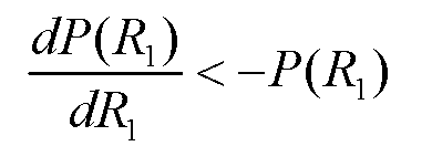


前記遮光膜の前記二領域間に電圧をかけるための電圧印加手段をさらに備えている。前記構成によると、遮光膜の前記二領域間に電圧をかけることで、貫通孔内部に検出対象を捕集することができる。そのため、検出感度がさらに向上する。
2 発光デバイス
3 検出器
4 第1の反射面
5 第2の反射面
6 導波路
7 遮光膜
7a 対向面
7b 出射面
8 貫通孔
9 検出対象
10 流路
11 窓
12 誘電体膜
101 光学センサヘッド
102 発光デバイス
103a 第1の検出器
103b 第2の検出器
104 第1の反射面
105 第2の反射面
106 導波路
108 駆動回路
109 温度センサ
120 反応体
151 算出部
152 表示部
200 光学センサシステム
Claims (8)
- 第1の反射面、前記第1の反射面と対向する第2の反射面、および、前記第1の反射面と前記第2の反射面との間に設けられた導波路を有する発光デバイスと、
前記第1の反射面上に形成された反応体と、
前記第1の反射面及び前記第2の反射面の一方から出射される光の光強度を検出する第1の検出器と、
前記第1の検出器によって検出された光強度に基づいて前記第1の反射面における環境パラメータを算出する算出部とを備えている光学センサシステムにおいて、
前記第1の反射面の反射率R1と、前記検出器によって検出された光強度P(R1)とが、

- 前記第1の検出器によって検出される光強度が一定となるよう、前記第1の検出器によって検出された光強度に基づいてフィードバック制御を行う制御手段をさらに備えていることを特徴とする請求項1に記載の光学センサシステム。
- 前記第1の反射面及び前記第2の反射面の他方から出射される光の光強度を検出する第2の検出器をさらに備えていることを特徴とする請求項1又は2に記載の光学センサシステム。
- 第1の反射面、前記第1の反射面と対向する第2の反射面、および、前記第1の反射面と前記第2の反射面との間に設けられた導波路が形成された発光デバイスと、
近接場光を発生させるための貫通孔が設けられた、前記第1の反射面上に形成された遮光膜と、
前記第1または第2の反射面を通して前記発光デバイスから出射される光の光強度を検出する検出器とを備えた光学センサヘッドであって、
前記遮光膜の光の出射面上での前記貫通孔の開口面積が、前記第1の反射面に対向した前記遮光膜の対向面上での前記貫通孔の開口面積よりも大きいことを特徴とする光学センサヘッド。 - 前記遮光膜が、表面プラズモンを励起する材料からなることを特徴とする請求項4に記載の光学センサヘッド。
- 前記発光デバイスから出射される光が直線偏光であり、
前記直線偏光の方向に関して、前記遮光膜の前記出射面上での前記貫通孔の開口長さが、前記遮光膜の前記対向面上での前記貫通孔の開口長さよりも大きいことを特徴とする請求項5に記載の光学センサヘッド。 - 前記発光デバイスから出射される光が直線偏光であり、
前記遮光膜の前記対向面上での前記直線偏光の方向に関する前記貫通孔の開口長さが、前記発光デバイスから出射される光の波長より小さいことを特徴とする請求項4又は5に記載の光学センサヘッド。 - 請求項4~7のいずれか1項に記載の光学センサヘッドと、
前記発光デバイスを発光させたときにおける前記検出器の検出値を元に、前記貫通孔内の屈折率を算出する算出部と、
前記算出部で算出された屈折率を表示する表示部とを備える光学センサシステム。
Priority Applications (2)
| Application Number | Priority Date | Filing Date | Title |
|---|---|---|---|
| JP2015500184A JP6002311B2 (ja) | 2013-02-14 | 2014-01-31 | 光学センサヘッド、および光学センサシステム |
| US14/766,145 US20150377788A1 (en) | 2013-02-14 | 2014-01-31 | Optical sensor head and optical sensor system |
Applications Claiming Priority (2)
| Application Number | Priority Date | Filing Date | Title |
|---|---|---|---|
| JP2013-026891 | 2013-02-14 | ||
| JP2013026891 | 2013-02-14 |
Publications (1)
| Publication Number | Publication Date |
|---|---|
| WO2014125943A1 true WO2014125943A1 (ja) | 2014-08-21 |
Family
ID=51353952
Family Applications (1)
| Application Number | Title | Priority Date | Filing Date |
|---|---|---|---|
| PCT/JP2014/052304 Ceased WO2014125943A1 (ja) | 2013-02-14 | 2014-01-31 | 光学センサヘッド、および光学センサシステム |
Country Status (3)
| Country | Link |
|---|---|
| US (1) | US20150377788A1 (ja) |
| JP (1) | JP6002311B2 (ja) |
| WO (1) | WO2014125943A1 (ja) |
Citations (5)
| Publication number | Priority date | Publication date | Assignee | Title |
|---|---|---|---|---|
| JP2001266389A (ja) * | 2000-03-23 | 2001-09-28 | Tdk Corp | 近接場光を用いる光ヘッド |
| JP2001274505A (ja) * | 2000-03-27 | 2001-10-05 | Olympus Optical Co Ltd | 半導体レーザ装置 |
| JP2005150144A (ja) * | 2003-11-11 | 2005-06-09 | Seiko Epson Corp | タイル状面発光レーザ、タイル状面発光レーザの製造方法、デバイス及び電子機器 |
| JP2008516257A (ja) * | 2004-10-13 | 2008-05-15 | ヒューレット−パッカード デベロップメント カンパニー エル.ピー. | 表面増強ラマン分光法のためのその場励起 |
| JP2010237020A (ja) * | 2009-03-31 | 2010-10-21 | Japan Aerospace Exploration Agency | 生体分子検出装置及び生体分子検出方法 |
Family Cites Families (3)
| Publication number | Priority date | Publication date | Assignee | Title |
|---|---|---|---|---|
| JP3991267B2 (ja) * | 2002-10-08 | 2007-10-17 | アークレイ株式会社 | 分析装置およびこれの製造方法 |
| JP4782777B2 (ja) * | 2004-05-11 | 2011-09-28 | テル アビブ ユニバーシティー フューチャー テクノロジー ディベロップメント エルティーディー. | 平面状の微小共振器に基づく光学的化学バイオセンサ |
| TWI385376B (zh) * | 2008-03-28 | 2013-02-11 | Delta Electronics Inc | 生物感測器 |
-
2014
- 2014-01-31 WO PCT/JP2014/052304 patent/WO2014125943A1/ja not_active Ceased
- 2014-01-31 US US14/766,145 patent/US20150377788A1/en not_active Abandoned
- 2014-01-31 JP JP2015500184A patent/JP6002311B2/ja not_active Expired - Fee Related
Patent Citations (5)
| Publication number | Priority date | Publication date | Assignee | Title |
|---|---|---|---|---|
| JP2001266389A (ja) * | 2000-03-23 | 2001-09-28 | Tdk Corp | 近接場光を用いる光ヘッド |
| JP2001274505A (ja) * | 2000-03-27 | 2001-10-05 | Olympus Optical Co Ltd | 半導体レーザ装置 |
| JP2005150144A (ja) * | 2003-11-11 | 2005-06-09 | Seiko Epson Corp | タイル状面発光レーザ、タイル状面発光レーザの製造方法、デバイス及び電子機器 |
| JP2008516257A (ja) * | 2004-10-13 | 2008-05-15 | ヒューレット−パッカード デベロップメント カンパニー エル.ピー. | 表面増強ラマン分光法のためのその場励起 |
| JP2010237020A (ja) * | 2009-03-31 | 2010-10-21 | Japan Aerospace Exploration Agency | 生体分子検出装置及び生体分子検出方法 |
Also Published As
| Publication number | Publication date |
|---|---|
| JP6002311B2 (ja) | 2016-10-05 |
| US20150377788A1 (en) | 2015-12-31 |
| JPWO2014125943A1 (ja) | 2017-02-02 |
Similar Documents
| Publication | Publication Date | Title |
|---|---|---|
| US8539816B2 (en) | Method and apparatus for locking a laser with a resonant cavity | |
| US8634078B2 (en) | Sensor, method for detecting the presence and/or concentration of an analyte using the sensor, and use of the method | |
| JP2002505425A (ja) | 導波路構造 | |
| JP2005508095A (ja) | Vcselを用いて刺激を測定する方法及び装置 | |
| JP2010206160A (ja) | 量子干渉装置、原子発振器、および磁気センサー | |
| WO2013161272A1 (ja) | 光学デバイス及び検出装置 | |
| Marschick et al. | Compact vertical emitting ring interband cascade lasers for isotope-resolved CO2 sensing | |
| US20040257965A1 (en) | Optical device and optical sensor | |
| JP6002311B2 (ja) | 光学センサヘッド、および光学センサシステム | |
| JP4728989B2 (ja) | ラマン散乱光増強デバイス | |
| CN119447993B (zh) | 边发射激光传感芯片及其制备方法 | |
| US6741352B2 (en) | Sensor utilizing attenuated total reflection | |
| JP6208236B2 (ja) | 光学センサシステム | |
| JP3454870B2 (ja) | 光学式変位センサ | |
| KR20130110900A (ko) | 표면 플라즈몬 공명을 이용한 다층 박막 센서 | |
| JP3844688B2 (ja) | 全反射減衰を利用したセンサー | |
| KR100831384B1 (ko) | 포토닉 결정을 사용하는 대상 물질 센서 및 대상 물질의 검출 방법 | |
| EP4517302A1 (en) | A volatile molecular components detection device | |
| CN119804391B (zh) | 一种片上光热气体传感器和片上气体传感器组件 | |
| US20240178628A1 (en) | Photoacoustic system and associated method | |
| US20240039247A1 (en) | Optoelectronic semiconductor device and method for operating an optoelectronic semiconductor device | |
| JP2010054621A (ja) | 波長変換光源 | |
| JPH0663866B2 (ja) | 波長検出装置 | |
| TWI404925B (zh) | 生物感測器 | |
| JP2015072157A (ja) | 光学素子、ラマン分光法、ラマン分光装置、および電子機器 |
Legal Events
| Date | Code | Title | Description |
|---|---|---|---|
| 121 | Ep: the epo has been informed by wipo that ep was designated in this application |
Ref document number: 14751118 Country of ref document: EP Kind code of ref document: A1 |
|
| ENP | Entry into the national phase |
Ref document number: 2015500184 Country of ref document: JP Kind code of ref document: A |
|
| WWE | Wipo information: entry into national phase |
Ref document number: 14766145 Country of ref document: US |
|
| NENP | Non-entry into the national phase |
Ref country code: DE |
|
| 122 | Ep: pct application non-entry in european phase |
Ref document number: 14751118 Country of ref document: EP Kind code of ref document: A1 |