WO2014123085A1 - 塗布膜形成方法、塗布膜形成装置及び記憶媒体 - Google Patents
塗布膜形成方法、塗布膜形成装置及び記憶媒体 Download PDFInfo
- Publication number
- WO2014123085A1 WO2014123085A1 PCT/JP2014/052439 JP2014052439W WO2014123085A1 WO 2014123085 A1 WO2014123085 A1 WO 2014123085A1 JP 2014052439 W JP2014052439 W JP 2014052439W WO 2014123085 A1 WO2014123085 A1 WO 2014123085A1
- Authority
- WO
- WIPO (PCT)
- Prior art keywords
- substrate
- wafer
- coating film
- coating
- mist
- Prior art date
- Legal status (The legal status is an assumption and is not a legal conclusion. Google has not performed a legal analysis and makes no representation as to the accuracy of the status listed.)
- Ceased
Links
Images


Classifications
-
- H—ELECTRICITY
- H10—SEMICONDUCTOR DEVICES; ELECTRIC SOLID-STATE DEVICES NOT OTHERWISE PROVIDED FOR
- H10P—GENERIC PROCESSES OR APPARATUS FOR THE MANUFACTURE OR TREATMENT OF DEVICES COVERED BY CLASS H10
- H10P72/00—Handling or holding of wafers, substrates or devices during manufacture or treatment thereof
- H10P72/04—Apparatus for manufacture or treatment
- H10P72/0448—Apparatus for applying a liquid, a resin, an ink or the like
-
- G—PHYSICS
- G03—PHOTOGRAPHY; CINEMATOGRAPHY; ANALOGOUS TECHNIQUES USING WAVES OTHER THAN OPTICAL WAVES; ELECTROGRAPHY; HOLOGRAPHY
- G03F—PHOTOMECHANICAL PRODUCTION OF TEXTURED OR PATTERNED SURFACES, e.g. FOR PRINTING, FOR PROCESSING OF SEMICONDUCTOR DEVICES; MATERIALS THEREFOR; ORIGINALS THEREFOR; APPARATUS SPECIALLY ADAPTED THEREFOR
- G03F7/00—Photomechanical, e.g. photolithographic, production of textured or patterned surfaces, e.g. printing surfaces; Materials therefor, e.g. comprising photoresists; Apparatus specially adapted therefor
- G03F7/16—Coating processes; Apparatus therefor
- G03F7/162—Coating on a rotating support, e.g. using a whirler or a spinner
-
- H—ELECTRICITY
- H10—SEMICONDUCTOR DEVICES; ELECTRIC SOLID-STATE DEVICES NOT OTHERWISE PROVIDED FOR
- H10P—GENERIC PROCESSES OR APPARATUS FOR THE MANUFACTURE OR TREATMENT OF DEVICES COVERED BY CLASS H10
- H10P72/00—Handling or holding of wafers, substrates or devices during manufacture or treatment thereof
- H10P72/04—Apparatus for manufacture or treatment
- H10P72/0431—Apparatus for thermal treatment
- H10P72/0434—Apparatus for thermal treatment mainly by convection
Definitions
- the present invention relates to the technical field of forming a coating film by spin coating.
- a spin coating method is generally used as a method for forming a coating film in a semiconductor manufacturing process.
- the spin coating method is a coating method in which a coating solution is supplied to the center of the surface of a semiconductor wafer (hereinafter referred to as a wafer) and spreads to the peripheral edge of the wafer by centrifugal force accompanying the rotational force of the substrate.
- the coating solution include a resist, a chemical solution for forming an antireflection film, or a chemical solution containing a silicon oxide film precursor.
- a method in which a rinse liquid such as pure water is discharged onto the back surface of the wafer and cooled by using the heat of vaporization of the rinse liquid.
- a rinse liquid such as pure water
- the centrifugal force generated by the rotation of the wafer water droplets of pure water are scattered in the cup body and drawn into the drainage channel, and the resist solution and water are mixed together to deposit and solidify the resist. For this reason, since the solidified material adheres to the drainage channel, there is a problem that the maintenance frequency is increased.
- the present invention has been made under such circumstances.
- the purpose of the present invention is to efficiently cool the substrate when forming the coating film by spin coating, and to suppress the scattering of water droplets into the cup body.
- an object of the present invention is to provide a technique for suppressing the precipitation of the solid content of the coating liquid in the discharge path.
- the coating film forming method of the present invention includes a step of horizontally holding a substrate on a substrate holding portion that is rotatable about a vertical axis, Thereafter, supplying a coating solution to the center of the substrate, and forming a coating film on the substrate by spreading by a centrifugal force due to rotation of the substrate; Supplying the mist that is a group of fine particles of liquid or solid to the lower surface side of the substrate before the coating solution reaches the peripheral edge of the substrate, and cooling the substrate; It is characterized by including.
- the coating film forming method of the present invention includes a step of horizontally holding a substrate on a substrate holding portion that is rotatable around a vertical axis, Next, rotating the substrate on the substrate holding unit, volatilizing the liquid by an air flow formed on the lower surface side of the substrate from the liquid storage unit facing the lower surface of the substrate, and cooling the substrate; Thereafter, supplying a coating solution to the center of the substrate, and forming a coating film on the substrate by spreading by a centrifugal force due to rotation of the substrate; It is characterized by including.
- the coating film forming apparatus of the present invention is a coating film forming apparatus that forms a coating film on the surface of a substrate by spin coating.
- a substrate holder for holding the substrate horizontally;
- a rotation mechanism for rotating the substrate holder around a vertical axis;
- a coating solution nozzle for supplying a coating solution to the substrate;
- a cup body provided to surround the substrate and connected to a drain path for discharging the coating liquid scattered by the rotation of the substrate and an exhaust path for exhausting the internal atmosphere;
- a mist supply unit for supplying mist which is a liquid or solid particle group to the lower surface side of the substrate;
- a control unit for outputting a control signal so as to discharge the mist from the mist supply unit before the coating liquid reaches the peripheral edge of the substrate; It is characterized by providing.
- the coating film forming apparatus of the present invention is a coating film forming apparatus that applies a coating liquid to the surface of a substrate and forms a coating film by spin coating.
- a substrate holder for holding the substrate horizontally;
- a rotation mechanism for rotating the substrate held by the substrate holding unit around a vertical axis;
- a coating solution nozzle for supplying a coating solution to the substrate held by the substrate holding unit;
- a cup body provided so as to surround the substrate and connected to a discharge path for discharging the coating liquid scattered by rotation of the substrate and an exhaust path for exhausting the internal atmosphere;
- a liquid container that opens to face the lower surface of the substrate and volatilizes the liquid by the airflow;
- a gas inlet for pulling the substrate onto the lower surface side of the substrate by the rotation of the substrate on the substrate holding portion to form an air flow.
- the storage medium of the present invention is a storage medium that stores a computer program used in a coating film forming apparatus that forms a coating film on a surface of a substrate by spin coating.
- the computer program has a set of steps so as to execute the above-described coating film forming method.
- the substrate when forming a coating film on a substrate by spin coating, the substrate is cooled by utilizing the vaporization (or sublimation) heat of mist, so that the cooling efficiency is high. Therefore, the rising of the coating film on the peripheral edge of the substrate can be suppressed while the amount of the coating liquid is small.
- mist since mist is used for cooling the substrate, it is possible to suppress the problem that solids are precipitated by mixing the coating liquid and liquid droplets scattered in the cup as in the case of back rinse. Can reduce the frequency of maintenance.
- a liquid container is provided below the substrate, the substrate on the substrate holder is rotated, and the liquid is volatilized by an air flow formed on the lower surface side of the substrate from the liquid container facing the lower surface of the substrate.
- Cooling is performed using heat of vaporization, so cooling efficiency is high, and since droplets are not directly discharged onto the substrate, the droplets do not scatter and the coating liquid scattered in the cup is mixed with the droplets. It is possible to suppress a problem that a solid matter is deposited.
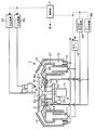
- 1 is a perspective view showing a resist coating apparatus according to a first embodiment. It is a block diagram which shows the resist coating device which concerns on 1st Embodiment. It is a top view which shows the resist coating device which concerns on 1st Embodiment. It is a vertical side view which shows the structure of a mist nozzle. It is a top view which shows the structure of a mist nozzle.
- 1st Embodiment it is explanatory drawing which matched the time chart and processing process of the rotation speed of a wafer. It is explanatory drawing which shows the coating film formation process of the coating film formation method of this invention. It is explanatory drawing which shows the coating film formation process of the coating film formation method of this invention.
- the resist coating apparatus includes a cup module 1 and a nozzle unit 2.
- the cup module 1 includes a spin chuck 11 that is a substrate holding unit that sucks and horizontally holds the center of the back surface of the wafer W, and the spin chuck 11 is connected to a rotating mechanism 13 via a rotating shaft 12 that extends vertically. Yes.
- the rotation mechanism 13 includes a rotation drive source such as a rotation motor (not shown), and is configured to rotate at a predetermined speed.
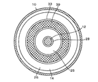
- a substantially disc-shaped partition plate 14 is provided below the spin chuck 11.
- the partition plate 14 includes a flat surface portion 25, a mountain-shaped portion 26 having a mountain-shaped cross section, and a vertical wall 27.
- the flat surface portion 25 is formed in a region narrower than a region where the wafer W is projected on the center side of the partition plate 14.
- a region outside the flat surface portion 25 is a chevron portion 26.
- the chevron portion 26 is formed in a chevron shape that is inclined in the center direction and the peripheral direction of the partition plate 14, and is provided so that the horizontal position of the highest portion is located closer to the center than the peripheral position of the wafer W. Yes.
- a region outside the chevron 26 is bent downward to form a vertical wall 27.
- a gap 28 is formed between the partition plate 14 and the rotary shaft 12, and the lower surface side of the wafer W becomes a negative pressure when the wafer W is rotated, and an airflow flows from the gap 28. Yes.
- a cup body 10 having an opening on the upper side so as to surround the spin chuck 11 is provided, and an upper end side of the side peripheral surface of the cup body 10 forms an inclined portion that is inclined inward.
- three elevating pins 19 are provided in the circumferential direction so as to protrude from the partition plate 14, and the elevating pins 19 are configured to be moved up and down by an elevating mechanism 20.
- an annular recess-shaped liquid receiving portion 15 having an upper opening is provided on the bottom side of the cup body 10.
- the liquid receiving portion 15 is partitioned into an outer region and an inner region over the entire circumference on the lower peripheral edge of the wafer W when the vertical wall 27 enters.
- a drainage path 16 that is a drainage path for draining a drain of stored resist or the like is provided at the bottom of the outer area, and a cylindrical exhaust path 17 that extends upward from the bottom is provided in the inner area.
- the upper end of the exhaust passage 17 opens at a position higher than the lower end of the vertical wall 27.
- One end of an exhaust pipe is connected to the lower end of the exhaust path 17, and the other end of the exhaust pipe is connected to, for example, a factory exhaust path via an exhaust damper 18.
- the exhaust damper 18 is for controlling the exhaust amount in the cup body 10 in response to a control signal from the control unit 7 described later.
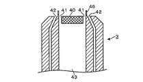
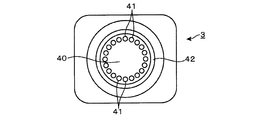
- a mist nozzle 3 that is a two-fluid nozzle corresponding to a mist supply unit is provided on the upper surface of the region of the flat surface portion 25 of the partition plate 14.
- the mist nozzles 3 are provided at four locations below the wafer W at equal intervals in the circumferential direction.
- the configuration of the mist nozzle 3 will be described with reference to FIGS.
- a large number of treatment liquid discharge holes 41 are arranged at equal intervals in the circumferential direction.
- a guide portion 46 is provided in the processing liquid discharge hole 41 so as to protrude from the processing liquid discharge hole 41.
- An annular gas discharge passage 42 is formed concentrically with the processing liquid supply passage 43 on the tube wall of the mist nozzle 3 surrounding the treatment liquid supply passage 43, and the tip of the gas discharge passage 42 is the center of the mist nozzle 3.
- the gas discharged from the gas discharge channel 42 is directed toward the shaft, and is discharged toward the processing liquid discharged from the processing liquid discharge hole 41.
- the processing liquid supply path 43 is connected to one end of a processing liquid supply pipe 44 that extends to the outside of the mist nozzle 3.
- a processing liquid supply mechanism 45 configured by, for example, a pump or a valve is connected to the other end of the processing liquid supply pipe 44, and a predetermined amount of processing liquid such as pure water can be discharged from the processing liquid discharge hole 41. It is configured as follows.
- the gas discharge passage 42 is connected to one end of a gas supply pipe 47, and the other end of the gas supply pipe 47 is connected to a gas supply mechanism 48 including, for example, a pump, a valve, a mass flow meter, and the like.
- a gas supply mechanism 48 including, for example, a pump, a valve, a mass flow meter, and the like.
- a predetermined amount of nitrogen gas can be discharged from the gas discharge passage 42.
- the mist nozzle 3 discharges pure water from the treatment liquid discharge hole 41 and discharges nitrogen gas from the gas discharge passage 42 toward the discharged pure water. It is presumed that fine water mist is formed by mixing the discharged pure water and the nitrogen gas as the carrier gas.
- the nozzle unit 2 is moved by a moving mechanism including an arm 21, a moving body 22, an elevating mechanism (not shown) and a guide rail 23, so that the discharge position above the central portion of the wafer W and the standby bus outside the cup body 10. It is comprised so that it may move between 24.
- a pre-wet nozzle 5 and a resist nozzle 6 that is a coating solution nozzle are provided at the tip of the nozzle unit 2.
- the pre-wet nozzle 5 is connected to a thinner supply mechanism 52 via a supply pipe 51.
- the thinner supply mechanism 52 includes devices such as a pump, a valve, and a filter, for example, and is configured to discharge a predetermined amount of thinner from the tip of the pre-wet nozzle 5.
- the resist nozzle 6 is connected to a resist supply mechanism 62 via a supply pipe 61.
- the resist supply mechanism 62 includes devices such as a pump, a valve, and a filter, and is configured to discharge a predetermined amount of resist solution from the tip of the resist nozzle 6.
- the resist coating apparatus is provided with a control unit 7 composed of, for example, a computer.
- the control unit 7 has a program storage unit.
- the wafer W is transferred between the external transfer arm and the spin chuck 11, the spin chuck 11 is rotated, the resist solution and the thinner.
- a program in which instructions are set so that a mist supply sequence is executed is stored.
- This program is stored in a storage medium such as a flexible disk, a compact disk, a hard disk, an MO (magneto-optical disk), or a memory card and installed in the control unit 7.
- FIG. 6 is a diagram showing an explanation in which the rotation time chart of the wafer W is associated with the processing steps.
- the rotation start time of the spin chuck 11 is set to 0 second. . 7 to 10 show the processing steps of the wafer W step by step.
- the wafer W is loaded into the resist coating apparatus by a transfer arm (not shown) provided outside the resist coating apparatus.
- the wafer W is placed on the spin chuck 11 by the cooperative action of the transfer arm and the three lifting pins 19 projecting and retracting from the partition plate 14.
- the term “surface of the wafer W” is used as a surface (upper surface) of the wafer W on which the coating liquid is discharged.
- the nozzle unit 2 moves as shown in FIG. 7 and the pre-wet nozzle 5 is positioned above the center of the wafer W.
- the rotation of the spin chuck 11 is started, and the wafer W is rotated for 3.5 seconds at a speed of 500 rpm, for example.
- the valves of the processing liquid supply mechanism 45 and the gas supply mechanism 48 are opened, the pump is driven, and a mist having a diameter of, for example, 100 ⁇ m or less is directed from the mist nozzle 3 toward the back surface of the wafer W. Sprayed (supplied) in the form of a spray.
- the diameter of the mist is 30 to 100 ⁇ m. This stage corresponds to the mist supply process of FIG.
- a mist of pure water having a fine size is sprayed from the mist nozzle 3 toward the back surface of the wafer W.
- the mist collides with the back surface of the wafer W rotating at high speed, and the mist group is vaporized into water vapor by the impact at the time of collision, and takes heat from the wafer W.
- the wafer W is rotating at high speed.
- a swirl flow is formed on the back surface side of the wafer W and a negative pressure is generated, and air is drawn from the gap 28 between the rotating shaft 12 and the partition plate 14, thereby forming a strong air flow from the center side of the wafer W to the outside. .
- the atmospheric temperature in the space also decreases.
- the wafer W is cooled with high efficiency.
- the temperature of the wafer W is cooled to, for example, 0.8 ° C. from the temperature (23 ° C.) in the clean room atmosphere to 22.2 ° C.
- the rotation of the wafer W is stopped as shown in FIG. 8, and, for example, a thinner 53 is supplied from the pre-wet nozzle 5 for 1.5 seconds. Thereafter, the wafer W is rotated at a speed of 2000 rpm for 0.5 seconds. As a result, the thinner supplied to the wafer W is stretched all at once from the center of the wafer W toward the peripheral edge by the centrifugal force generated by the high-speed rotation of the wafer W, and the entire surface of the wafer W becomes wet.
- These steps correspond to the thinner discharge step and the thinner extension step of FIG. In the thinner discharge process, the supply of mist from the mist nozzle 3 has already stopped, but the wafer W is further cooled by vaporization of the staying mist.
- the resist nozzle 6 is moved so as to be positioned above the center of the wafer W, and the rotation speed of the wafer W is increased to a first rotation speed, for example, 2500 rpm. Simultaneously with the increase in the rotation speed, for example, 0.5 cc of a resist solution is discharged from the resist nozzle 6 to the center of the wafer W, and the rotation of the wafer W is maintained for 2 seconds.
- This stage corresponds to the resist discharge extension process of FIG. 6, and the resist solution 63 spreads from the center along the surface of the wafer W by centrifugal force as shown in FIG.
- the rotation speed of the wafer W is lowered to a second rotation speed, for example, 100 rpm, and maintained in this state for 1 second.
- This process corresponds to the reflow process of FIG. 6, and the resist solution 63 is biased toward the outer periphery by the spreading process, and the film acting by reducing the centrifugal force acting on the wafer W against the resist film having a non-uniform film thickness. This is done to adjust the thickness.
- the rotation speed of the wafer W is increased to a third rotation speed, for example, 1500 rpm, and maintained in this state for 20 seconds, for example.
- a third rotation speed for example, 1500 rpm
- the resist solution 63 is dried while being gradually extended, and after reaching the third rotation speed, the resist solution 63 reaches the outer periphery of the wafer W at about 4 seconds later.
- the temperature of the wafer W continues to decrease for about 12 seconds after the supply of mist is stopped.
- the wafer W has a temperature of about 20.0 ° C. It has become.
- the temperature of the wafer W is lowered before spreading the resist solution on the surface of the wafer W. Therefore, the solvent in the coating solution spread on the surface of the wafer W is less likely to volatilize. Therefore, even when the resist solution supplied to the wafer W is small, the decrease in the content of the solvent in the resist solution is suppressed, and the decrease in the fluidity of the resist solution is suppressed. Therefore, even when the supply of the resist solution to the wafer W is small, the rising of the resist film on the peripheral edge of the wafer W can be reduced.
- the timing at which the mist starts to be supplied from the mist nozzle 3 to the back surface of the wafer W is before the time when the reflow shown in FIG.
- the resist solution is before the time when the resist solution is supplied to the wafer W.
- the wafer W is not limited to being cooled immediately after the reflow, but may be cooled before the resist solution reaches the periphery of the wafer W. In this case, the supply of mist may be started before the resist solution spreads so as to cover 70% of the area of the wafer W.
- the temperature of the wafer W continues to decrease for about 12 seconds after the supply of mist. Therefore, the supply of mist is preferably finished 10 seconds before the point when the resist solution reaches the outer periphery of the wafer W, and preferably 15 seconds or less at the earliest.
- the mist supply position on the back surface of the wafer W may be changed to a position closer to the center or a position closer to the periphery.
- the mist nozzle 3 is configured to be able to move on the partition plate 14 along a guide extending from the center to the peripheral direction. Since the mist can be supplied to a wider range by supplying the mist while changing the supply position of the mist while the wafer W is rotated, the wafer W can be cooled more uniformly.
- the mist preferably has a size that vaporizes quickly after contacting the wafer W, at least a size that does not agglomerate as droplets on the back surface of the wafer W, and its diameter is preferably, for example, 100 ⁇ m or less.
- the mist nozzle 3 may be a one-fluid mist nozzle 3. As such an example, an example in which a porous body is provided at the tip of the mist nozzle 3 can be given.
- the mist may be a solid particle group, and may be cooled by supplying, for example, a dry ice particle group.
- the coating film forming apparatus may be a pipe in which the exhaust path and the drainage path are shared, or may be configured to be branched in the middle of the pipe.
- FIGS. 11 and 12 A coating film forming apparatus according to the second embodiment will be described.
- a partition plate 14 corresponding to the facing surface portion is provided in the cup body 10, and a ring shape is provided on the upper surface of the flat surface portion 25 of the partition plate 14 so as to surround the periphery of the rotating shaft 12.
- the liquid container 33 is provided.
- the liquid container 33 is formed to a depth of 5 mm, for example, and the distance between the water surface and the wafer W when the liquid container 33 is filled with the liquid is set to about 15 mm.
- a pure water supply pipe 35 is connected to the liquid storage unit 33, and the other end side of the pure water supply pipe 35 is connected to a pure water supply mechanism 37 including devices such as a pump, a valve, and a filter.
- the liquid container 33 is configured to supply predetermined pure water.
- a porous member 39 is provided on the upper surface of the liquid storage portion 33.
- the cup body 10 surrounding the periphery of the wafer W is provided with a flat surface portion 25, a mountain-shaped portion 26, and a vertical wall 27 on the partition plate 14 in the same manner as described in FIG.
- An annular recess-shaped liquid receiving portion 15 is formed in the exhaust passage 17 and the exhaust passage 17.
- the exhaust passage 17 is provided with an exhaust damper 18.
- a gap 28 is provided between the partition plate 14 and the rotary shaft 12.
- an amount of water used for cooling one wafer W is supplied to the liquid storage unit 33.
- One wafer W is the amount of water set so that no water remains in the liquid storage portion 33 when the coating film forming step shown in FIG.
- the wafer W is rotated at a speed of 3000 rpm. Therefore, a swirl flow is formed on the lower surface side of the wafer W, and the lower surface side of the wafer W becomes a negative pressure as shown in FIG. For this reason, in combination with the suction action to the exhaust passage 17 shown in FIG.
- the amount of water stored in the liquid storage unit 33 may be an amount of water that is emptied when the process of rotating the wafer W for cooling the wafer W is completed before the thinner is discharged. Furthermore, the liquid container 33 may store an amount of water sufficient to cool a plurality of wafers W sequentially loaded. Alternatively, a fixed amount of water equal to or more than the amount of water for cooling one wafer W is stored in the liquid storage unit 33 for each wafer W, and after the formation of the coating film on the wafer W is completed, the water in the liquid storage unit 33 is drained. When the next wafer W is discharged and carried into the spin chuck 11, the predetermined amount of water may be stored in the liquid storage unit 33.
- the wafer W can be cooled using the vaporization heat of pure water, so that it can be efficiently cooled. Further, since cooling is performed using the heat of vaporization of pure water stored in the liquid storage unit 33, it is possible to prevent water droplets from being scattered into the cup body 10 due to the centrifugal force caused by the rotation of the wafer W. Effects can be obtained.
- Example 1 In order to evaluate the present invention, the following tests were conducted using the resist coating apparatus shown in the embodiment of the present invention.
- Various coolants are supplied from the surface side to a measuring wafer (12 inches in diameter) provided with temperature sensors at 65 locations from the center to the periphery, and simultaneously the wafer W is rotated, and the temperature of the wafer W is measured for each coolant. The transition was examined.
- This wafer is provided with a controller for storing temperature detection data of the temperature sensor, and an average value of 65 temperature detection values is handled as the wafer temperature.
- Example 1-1 At the same time as rotating the wafer at a rotation speed of 300 rpm, a mist of pure water was sprayed for 10 seconds toward a position displaced from the center of the wafer W by 7.5 cm (the wafer is rotating during the mist injection).
- Example 1-2 The same processing as in Example 1-1 was performed except that the rotation speed of the wafer W was 900 rpm.
- Comparative Example 1-2 Except that the refrigerant supplied to the wafer W was cyclohexane, the same processing as in Comparative Example 1-1 was performed.
- Comparative Example 1-3 The same processing as in Comparative Example 1-1 was performed, except that the refrigerant supplied to the wafer W was a PGME (propylene glycol monomethyl ether) / PGMEA (propylene glycol monomethyl ether acetate) mixture.
- PGME propylene glycol monomethyl ether
- PGMEA propylene glycol monomethyl ether acetate
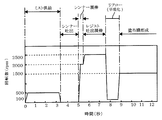
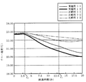
- FIG. 14 shows the temperature transition of the wafer in each example described above, with the elapsed time after the start of rotation of the wafer as the horizontal axis and the temperature of the wafer W as the vertical axis.
- a timing (t 0 ) corresponding to 3 seconds on the horizontal axis is a mist supply start time, and a timing (t 1 ) indicates a mist supply stop time.
- Example 1-1 the temperature of the wafer W continues to decrease until about 10 seconds after the start of the supply of mist, and decreases to about 22.0 ° C.
- the temperature of the wafer was about 22.0 ° C. when 3.5 seconds had elapsed after the mist supply. Thereafter, the temperature continued to decrease, and when the supply of mist was stopped, Example 1-1 was lowered to 21.2 ° C. and Example 1-2 was lowered to 20.8 ° C. Even after the supply of mist is stopped, the temperature of the wafer in each example continues to decrease, and at the time point 20 seconds after the start of rotation of the wafer, Example 1-1 is 20.5 ° C.
- the coating film forming method of the present invention it can be said that the wafer W can be cooled to a lower temperature.
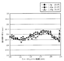
- FIG. 15 shows a case where, in the coating film forming method according to the first embodiment, the average temperature of the wafer (18 inches in diameter) is cooled to 23 ° C. and then the coating film is formed with 1.5 g of a resist solution.
- the coating film is formed with 1.42 g of resist solution after the average temperature is cooled to 21.5 ° C.
- the coating film is formed with 1.35 g of resist solution after the average temperature of the wafer is cooled to 20 ° C.
- the horizontal axis represents the distance from the center of the wafer
- the vertical axis represents the film thickness of the formed coating film.
- the film thickness at the peripheral edge of the wafer can be suppressed even with a small amount of resist.
- the resist solution is reduced by about 10%, and it is proved that the use of the resist can be suppressed by cooling the wafer W.
Landscapes
- Physics & Mathematics (AREA)
- General Physics & Mathematics (AREA)
- Coating Apparatus (AREA)
- Application Of Or Painting With Fluid Materials (AREA)
- Materials For Photolithography (AREA)
- Exposure Of Semiconductors, Excluding Electron Or Ion Beam Exposure (AREA)
Applications Claiming Priority (2)
| Application Number | Priority Date | Filing Date | Title |
|---|---|---|---|
| JP2013021416A JP5900370B2 (ja) | 2013-02-06 | 2013-02-06 | 塗布膜形成方法、塗布膜形成装置及び記憶媒体 |
| JP2013-021416 | 2013-02-06 |
Publications (1)
| Publication Number | Publication Date |
|---|---|
| WO2014123085A1 true WO2014123085A1 (ja) | 2014-08-14 |
Family
ID=51299680
Family Applications (1)
| Application Number | Title | Priority Date | Filing Date |
|---|---|---|---|
| PCT/JP2014/052439 Ceased WO2014123085A1 (ja) | 2013-02-06 | 2014-02-03 | 塗布膜形成方法、塗布膜形成装置及び記憶媒体 |
Country Status (3)
| Country | Link |
|---|---|
| JP (1) | JP5900370B2 (enExample) |
| TW (1) | TW201436882A (enExample) |
| WO (1) | WO2014123085A1 (enExample) |
Cited By (3)
| Publication number | Priority date | Publication date | Assignee | Title |
|---|---|---|---|---|
| CN108855776A (zh) * | 2017-05-08 | 2018-11-23 | 致伸科技股份有限公司 | 离心注胶系统及其方法 |
| CN110560327A (zh) * | 2018-06-05 | 2019-12-13 | 深圳市旭控科技有限公司 | 一种硅片涂源装置 |
| CN112415854A (zh) * | 2020-11-23 | 2021-02-26 | 华虹半导体(无锡)有限公司 | 改善晶圆光刻胶涂布效果的方法 |
Families Citing this family (10)
| Publication number | Priority date | Publication date | Assignee | Title |
|---|---|---|---|---|
| JP5886935B1 (ja) * | 2014-12-11 | 2016-03-16 | 東京エレクトロン株式会社 | 塗布処理方法、コンピュータ記憶媒体及び塗布処理装置 |
| DE102015100579A1 (de) * | 2015-01-15 | 2016-07-21 | Ev Group E. Thallner Gmbh | Verfahren und Vorrichtung zum Beschichten von Substraten |
| JP6212066B2 (ja) * | 2015-03-03 | 2017-10-11 | 東京エレクトロン株式会社 | 塗布処理方法、コンピュータ記憶媒体及び塗布処理装置 |
| JP6059793B2 (ja) * | 2015-12-11 | 2017-01-11 | 東京エレクトロン株式会社 | 塗布処理方法、コンピュータ記憶媒体及び塗布処理装置 |
| JP6728009B2 (ja) * | 2016-09-26 | 2020-07-22 | 株式会社Screenホールディングス | 基板処理方法および基板処理装置 |
| JP7202968B2 (ja) | 2019-05-09 | 2023-01-12 | 東京エレクトロン株式会社 | 塗布処理方法、塗布処理装置及び記憶媒体 |
| JP7344726B2 (ja) * | 2019-09-13 | 2023-09-14 | 東京エレクトロン株式会社 | 塗布処理方法、塗布処理装置及び記憶媒体 |
| CN114653503A (zh) * | 2020-12-23 | 2022-06-24 | 盛美半导体设备(上海)股份有限公司 | 涂胶机及其工艺腔 |
| JP7840221B2 (ja) * | 2022-07-05 | 2026-04-03 | 東京エレクトロン株式会社 | 液処理装置 |
| JP2024060970A (ja) | 2022-10-20 | 2024-05-07 | 東京エレクトロン株式会社 | カップ、液処理装置及び液処理方法 |
Citations (7)
| Publication number | Priority date | Publication date | Assignee | Title |
|---|---|---|---|---|
| JPH0462831A (ja) * | 1990-06-25 | 1992-02-27 | Toshiba Corp | ホトレジスト塗布方法 |
| JPH04363169A (ja) * | 1991-05-08 | 1992-12-16 | Hitachi Ltd | フォトレジストの塗布方法 |
| JPH0945611A (ja) * | 1995-07-27 | 1997-02-14 | Dainippon Screen Mfg Co Ltd | 回転式基板塗布装置 |
| JP2000124120A (ja) * | 1998-10-14 | 2000-04-28 | Tokyo Electron Ltd | 塗布処理方法 |
| US6548111B1 (en) * | 1999-06-08 | 2003-04-15 | Micron Technology, Inc. | Method for controlling a temperature of a microelectronic substrate |
| JP2004275887A (ja) * | 2003-03-14 | 2004-10-07 | Tokyo Electron Ltd | 塗布装置及び塗布方法 |
| JP2009220046A (ja) * | 2008-03-17 | 2009-10-01 | Seiko Epson Corp | 塗布装置 |
Family Cites Families (3)
| Publication number | Priority date | Publication date | Assignee | Title |
|---|---|---|---|---|
| JPH01204421A (ja) * | 1988-02-10 | 1989-08-17 | Hitachi Ltd | ホトレジスト塗布方法 |
| JP4597847B2 (ja) * | 2005-11-28 | 2010-12-15 | 株式会社フジクラ | 成膜装置 |
| JP5511451B2 (ja) * | 2010-03-16 | 2014-06-04 | 中央発條株式会社 | 自動車用スタビライザの製造方法 |
-
2013
- 2013-02-06 JP JP2013021416A patent/JP5900370B2/ja active Active
-
2014
- 2014-01-28 TW TW103103249A patent/TW201436882A/zh unknown
- 2014-02-03 WO PCT/JP2014/052439 patent/WO2014123085A1/ja not_active Ceased
Patent Citations (7)
| Publication number | Priority date | Publication date | Assignee | Title |
|---|---|---|---|---|
| JPH0462831A (ja) * | 1990-06-25 | 1992-02-27 | Toshiba Corp | ホトレジスト塗布方法 |
| JPH04363169A (ja) * | 1991-05-08 | 1992-12-16 | Hitachi Ltd | フォトレジストの塗布方法 |
| JPH0945611A (ja) * | 1995-07-27 | 1997-02-14 | Dainippon Screen Mfg Co Ltd | 回転式基板塗布装置 |
| JP2000124120A (ja) * | 1998-10-14 | 2000-04-28 | Tokyo Electron Ltd | 塗布処理方法 |
| US6548111B1 (en) * | 1999-06-08 | 2003-04-15 | Micron Technology, Inc. | Method for controlling a temperature of a microelectronic substrate |
| JP2004275887A (ja) * | 2003-03-14 | 2004-10-07 | Tokyo Electron Ltd | 塗布装置及び塗布方法 |
| JP2009220046A (ja) * | 2008-03-17 | 2009-10-01 | Seiko Epson Corp | 塗布装置 |
Cited By (4)
| Publication number | Priority date | Publication date | Assignee | Title |
|---|---|---|---|---|
| CN108855776A (zh) * | 2017-05-08 | 2018-11-23 | 致伸科技股份有限公司 | 离心注胶系统及其方法 |
| CN108855776B (zh) * | 2017-05-08 | 2020-08-14 | 致伸科技股份有限公司 | 离心注胶系统及其方法 |
| CN110560327A (zh) * | 2018-06-05 | 2019-12-13 | 深圳市旭控科技有限公司 | 一种硅片涂源装置 |
| CN112415854A (zh) * | 2020-11-23 | 2021-02-26 | 华虹半导体(无锡)有限公司 | 改善晶圆光刻胶涂布效果的方法 |
Also Published As
| Publication number | Publication date |
|---|---|
| JP2014151249A (ja) | 2014-08-25 |
| JP5900370B2 (ja) | 2016-04-06 |
| TW201436882A (zh) | 2014-10-01 |
Similar Documents
| Publication | Publication Date | Title |
|---|---|---|
| JP5900370B2 (ja) | 塗布膜形成方法、塗布膜形成装置及び記憶媒体 | |
| US8375887B2 (en) | Solution treatment apparatus, solution treatment method and resist coating method | |
| CN100595887C (zh) | 涂敷设备和涂敷方法 | |
| TWI757316B (zh) | 液體處理裝置及液體處理方法 | |
| US20190067041A1 (en) | Substrate processing apparatus, substrate processing method, and storage medium | |
| US20150004311A1 (en) | Coating film forming apparatus, coating film forming method, and recording medium | |
| JP2014151249A5 (enExample) | ||
| TW201714212A (zh) | 基板處理裝置,基板處理方法及記錄媒體 | |
| CN112013633B (zh) | 衬底处理方法及衬底处理装置 | |
| JP5682521B2 (ja) | 周縁部塗布装置、周縁部塗布方法及び記憶媒体 | |
| JP2009277795A (ja) | 塗布装置、塗布方法及び記憶媒体 | |
| JP3315608B2 (ja) | 塗布液塗布方法 | |
| JP5327238B2 (ja) | 塗布処理装置、塗布処理方法及び記憶媒体 | |
| JP5807622B2 (ja) | 塗布膜形成方法、塗布膜形成装置、基板処理装置及び記憶媒体 | |
| JP2004039828A (ja) | 塗布膜形成方法およびプリウェット剤 | |
| JP2017094324A (ja) | 塗布膜形成方法、塗布膜形成装置及び記憶媒体 | |
| US6576055B2 (en) | Method and apparatus for controlling air over a spinning microelectronic substrate | |
| JP6297452B2 (ja) | 基板処理装置、基板処理方法、及び記憶媒体 | |
| JP6432644B2 (ja) | 塗布膜形成装置、塗布膜形成方法、記憶媒体 | |
| CN112786484A (zh) | 基片处理方法和基片处理装置 | |
| JP6690717B2 (ja) | 塗布方法、塗布装置及び記憶媒体 | |
| JP2017161781A (ja) | 基板処理方法、基板処理装置及び記憶媒体 | |
| JP2015216168A (ja) | 塗布膜形成装置、塗布膜形成方法、記憶媒体 | |
| JP2021132103A (ja) | 基板処理方法及び基板処理装置 | |
| JP2001068402A (ja) | 基板処理装置 |
Legal Events
| Date | Code | Title | Description |
|---|---|---|---|
| 121 | Ep: the epo has been informed by wipo that ep was designated in this application |
Ref document number: 14748794 Country of ref document: EP Kind code of ref document: A1 |
|
| NENP | Non-entry into the national phase |
Ref country code: DE |
|
| 122 | Ep: pct application non-entry in european phase |
Ref document number: 14748794 Country of ref document: EP Kind code of ref document: A1 |