WO2014122838A1 - 筐体および無線通信装置 - Google Patents
筐体および無線通信装置 Download PDFInfo
- Publication number
- WO2014122838A1 WO2014122838A1 PCT/JP2013/081634 JP2013081634W WO2014122838A1 WO 2014122838 A1 WO2014122838 A1 WO 2014122838A1 JP 2013081634 W JP2013081634 W JP 2013081634W WO 2014122838 A1 WO2014122838 A1 WO 2014122838A1
- Authority
- WO
- WIPO (PCT)
- Prior art keywords
- housing
- hole
- conductive pattern
- circuit board
- injection material
- Prior art date
- Legal status (The legal status is an assumption and is not a legal conclusion. Google has not performed a legal analysis and makes no representation as to the accuracy of the status listed.)
- Ceased
Links
Images


Classifications
-
- H—ELECTRICITY
- H01—ELECTRIC ELEMENTS
- H01Q—ANTENNAS, i.e. RADIO AERIALS
- H01Q1/00—Details of, or arrangements associated with, antennas
- H01Q1/12—Supports; Mounting means
- H01Q1/22—Supports; Mounting means by structural association with other equipment or articles
- H01Q1/24—Supports; Mounting means by structural association with other equipment or articles with receiving set
- H01Q1/241—Supports; Mounting means by structural association with other equipment or articles with receiving set used in mobile communications, e.g. GSM
- H01Q1/242—Supports; Mounting means by structural association with other equipment or articles with receiving set used in mobile communications, e.g. GSM specially adapted for hand-held use
-
- H—ELECTRICITY
- H05—ELECTRIC TECHNIQUES NOT OTHERWISE PROVIDED FOR
- H05K—PRINTED CIRCUITS; CASINGS OR CONSTRUCTIONAL DETAILS OF ELECTRIC APPARATUS; MANUFACTURE OF ASSEMBLAGES OF ELECTRICAL COMPONENTS
- H05K5/00—Casings, cabinets or drawers for electric apparatus
- H05K5/02—Details
- H05K5/0247—Electrical details of casings, e.g. terminals, passages for cables or wiring
-
- H—ELECTRICITY
- H01—ELECTRIC ELEMENTS
- H01Q—ANTENNAS, i.e. RADIO AERIALS
- H01Q1/00—Details of, or arrangements associated with, antennas
- H01Q1/36—Structural form of radiating elements, e.g. cone, spiral, umbrella; Particular materials used therewith
- H01Q1/38—Structural form of radiating elements, e.g. cone, spiral, umbrella; Particular materials used therewith formed by a conductive layer on an insulating support
-
- H—ELECTRICITY
- H05—ELECTRIC TECHNIQUES NOT OTHERWISE PROVIDED FOR
- H05K—PRINTED CIRCUITS; CASINGS OR CONSTRUCTIONAL DETAILS OF ELECTRIC APPARATUS; MANUFACTURE OF ASSEMBLAGES OF ELECTRICAL COMPONENTS
- H05K5/00—Casings, cabinets or drawers for electric apparatus
- H05K5/06—Hermetically-sealed casings
- H05K5/069—Other details of the casing, e.g. wall structure, passage for a connector, a cable, a shaft
Definitions
- the present invention relates to a housing for storing a circuit board and a wireless communication device.
- Non-Patent Document 1 describes that a conductive pattern is provided in a tapered through hole using an LDS (Laser Direct Structure) method using light (laser) irradiation.
- LDS Laser Direct Structure
- the shape of the through-hole through which the conductive pattern passes is tapered, and is formed so as to open toward the inside of the housing so as not to be noticeable when viewed from the outside.
- FIG. 4A and an enlarged view of FIG. 4B it opens toward the inside of the housing 103 (B side in the figure) so that it is not noticeable when viewed from the outside.
- the through-hole 101 is filled with the injection material 102 in the housing 103 having the tapered through-hole 101 formed so that the pressure is applied from the outside of the housing 103 (A side in the figure). Therefore, there is a problem that the injection material 102 cannot be supported, and the injection material 102 comes off inside the housing 103 (B side in the figure).
- the housing 103 has a cylindrical through-hole 111 as shown in FIG.
- the injecting material 102 comes out of the inside of the housing 103 (B side in the figure), the waterproof and dustproof performance deteriorates, and the injecting material 102 moves around in the housing 103, and components such as the circuit board 104 are removed. There is a risk of damage or breakage. Therefore, a technique for suitably closing the through hole of the housing 103 is required.
- the present invention has been made in view of the above problems, and has as its main object to provide a technique for suitably closing a through hole in a housing having a through hole for allowing a conductive pattern to pass therethrough.
- a housing is a housing for storing a circuit board therein, and has a through hole that opens to the outside and the inside of the housing.
- a conductive pattern that is routed from the outer surface of the housing through the inner wall of the through hole to the inner surface of the housing and is conducted to the circuit board; and a plug member that closes the through hole.
- the opening outside the casing in the through hole is larger than the opening inside the casing in the through hole.
- the opening on the outside of the housing in the through hole is larger than the opening on the inside of the housing in the through hole. It has a shape that supports it. Thereby, it is possible to prevent the plug member from being detached when pressure is applied from the outside of the housing, and it is possible to suitably close the through hole.
- (A) is a figure which shows the portable terminal which concerns on Embodiment 1 of this invention
- (b) is the figure which expanded the circumference
- (A) is a figure which shows the portable terminal which concerns on a reference example
- (b) is the figure which expanded the circumference
- (c) is a through-hole in another reference example. It is the figure which expanded the circumference
- FIG. 1 (Configuration of mobile terminal 20)
- A) of FIG. 1 is a figure which shows the portable terminal (wireless communication apparatus) 20 which concerns on Embodiment 1 of this invention
- (b) is the figure which expanded the through-hole 1 of (a).
- the mobile terminal 20 stores a circuit board 4 for wireless communication inside the housing 3 and functions as a mobile terminal by hardware and software mounted on the circuit board 4.
- the housing 3 includes a through hole 1, an injection material (plug member) 2, and a conductive pattern 5.
- the conductive pattern 5 is connected to the circuit board 4 via the connector 6, and the mobile terminal 20 has a function of performing wireless communication using the conductive pattern 5 as an antenna.
- the housing 3 is a structure made of a dielectric, and can be formed of, for example, resin.
- the conductive pattern means a film-like or plate-like conductor formed in an arbitrary shape.
- the conductive pattern 5 is provided on the surface of the housing 3, passes through the inner wall of the through-hole 1, and passes from the inner surface (B side in the drawing) of the housing 3 to the outer side (A side in the drawing). It is drawn around to the surface. That is, the conductive pattern 5 provided on the inner wall of the through hole 1 is conductively connected between two surfaces (surfaces on the A side and B side of the housing 3 in the figure) where the through hole 1 opens.
- the conductive pattern 5 can be formed by using an LDS (Laser Direct Structure) method. That is, an organic metal is mixed with the resin constituting the housing 3 and the region on the housing 3 where the conductive pattern 5 is to be formed is irradiated with laser to deposit plating on the laser irradiation portion or the laser irradiation portion. As a result, the plating is bonded to the laser irradiation portion and the conductive pattern 5 can be formed.
- the substance which comprises the conductive pattern 5 is not specifically limited, What is necessary is just to use the substance (for example, metals, such as copper plating and nickel plating) which has electroconductivity.
- the through hole 1 has an inclined taper shape when irradiating the inner wall of the through hole 1 with a laser.
- the through-hole 1 is a hole provided so as to penetrate the housing 3, and connects the conductive patterns 5 attached to the outside (A side in the drawing) and the inside (B side in the drawing) of the housing 3.
- the housing 3 is formed so as to open to the outside (A side in the figure) and inside (B side in the figure).
- the opening on the outer side (A side in the drawing) of the housing 3 in the through hole 1 is more than the opening on the inner side (B side in the drawing) in the through hole 1. It is formed to be large. More specifically, it has a tapered shape that tapers (diameter narrows) from the outside (A side in the figure) to the inside (B side in the figure) of the housing 3.
- each opening part of the through-hole 1 is not limited, For example, in addition to a circle, an ellipse, a polygon (including a triangle and a quadrangle), a circle or a shape in which an ellipse and a polygon are combined, and the like can be given. .
- the injection material 2 is provided so as to close the through hole 1 in order to realize a waterproof and dustproof function for the inside of the housing 3 of the mobile terminal 20.
- the injection material 2 is a viscous liquid or gel at the time of injection, and may be solidified (dried) after being injected into the through hole 1.
- Such an injection material 2 is not particularly limited, and examples thereof include liquid glue, resin-based pressure-sensitive adhesive, adhesive, and reinforcing material.
- the injection material 2 may be an insulator or may have conductivity.
- the through hole 1 has an inclined taper shape when the injection material 2 is injected into the through hole 1.
- the opening on the outside (A side in the drawing) of the housing 3 in the through hole 1 is larger than the opening on the inside (B side in the drawing) in the through hole 1. It is formed as follows. With such a structure, the through-hole 1 can support the injection material 2 from the inside of the housing 3 (B side in the drawing), and therefore pressure is applied from the outside of the housing 3 (A side in the drawing). However, the injection material 2 does not come off and enter the inside of the housing 3.
- the through hole 1 physically supports the injection material 2
- the design restriction on the material of the injection material 2 is reduced, and the injection material 2 is a low-loss body.
- Various substances can be used in accordance with applications and specifications, such as those having desired functions such as those that can reduce costs.
- the opening on the outer side (A side in the drawing) of the housing 3 in the through hole 1 is more open than the opening on the inner side (B side in the drawing) in the through hole 1. Therefore, the distance 33 between the contact point 32 of the conductive pattern 5 and the connector 6 and the through hole center 31 is shorter than that in the case where the opening on the inner side (B side in the figure) of the through hole 1 is larger. can do. This is because the contact 32 cannot be provided near the center 31 of the through hole if the opening inside the housing 3 in the through hole 1 (B side in the figure) becomes large. Thereby, the length of the conductive pattern 5 required inside the housing
- the length of the conductive pattern 5 routed from the contact 32 to the slope opposite to the through hole 1 can be shortened.
- the length of the conductive pattern 5 (antenna element) disposed on the outer side (A side in the drawing) of the housing 3 can be increased.
- the antenna element can be disposed outside the housing 3 and the distance from the metal such as the circuit board 4 can be increased, so that the antenna performance can be improved.
- the conductive pattern 5 can be used for various uses other than the use as an antenna element.
- the conductive pattern 5 can be used to conductively connect the inside (B side in the figure) and the outside (A side in the figure) of the housing 3.
- a ground such as a sheet metal is disposed outside the housing 3 (A side in the figure) and is electrically connected to the conductive pattern 5, thereby electrically connecting the ground such as the sheet metal and the circuit board 4 via the conductive pattern 5. Can be connected to.
- the method for forming the conductive pattern 5 is not limited to the LDS method.
- a conductive paste, conductive ink, or the like may be printed on the housing 3, a MID (Molded Interconnect Devices) method may be used, or a conductive thin film may be attached to the housing 3.
- MID Molded Interconnect Devices
- the member that closes the through hole 1 is not limited to the injection material 2 injected into the through hole 1, and may be a plug member that becomes a plug that closes the through hole 1.
- the plug member can be, for example, an elastic body inserted into the through hole 1.
- Embodiment 2 The following will describe another embodiment of the present invention with reference to FIG. For convenience of explanation, members having the same functions as those described in the embodiment are given the same reference numerals, and descriptions thereof are omitted. Moreover, the modification in Embodiment 1 can be applied similarly.
- FIG. 2 is an enlarged view of the periphery of the through hole 11 according to the second embodiment of the present invention.
- the through hole 11 has a step whose diameter decreases from the outside (A side in the drawing) to the inside (B side in the drawing) of the housing 3, and the housing in the through hole 11.
- the opening portion on the outer side (A side in the drawing) of 3 is larger than the opening portion on the inner side (B side in the drawing) in the through hole 11.
- the through-hole 11 supports the injection material 2 from the inner side (B side in the figure) of the casing 3, so that pressure is applied from the outer side (A side in the figure) of the casing 3.
- the through hole has a tapered shape, the size of the opening on the outer side (A side in the drawing) of the housing 3 in the through hole 11 does not change even when the thickness of the housing 3 increases.
- Embodiment 3 The following will describe another embodiment of the present invention with reference to FIG.
- members having the same functions as those described in the first embodiment are denoted by the same reference numerals and description thereof is omitted.
- the modification in Embodiment 1 can be applied similarly.
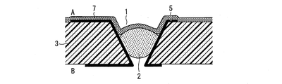
- FIG. 3 is an enlarged view of the periphery of the through hole 1 according to the third embodiment of the present invention.
- the shape of the through hole 1 is a mortar shape whose diameter increases toward the outside of the housing 3 (A side in the drawing), as in the first embodiment.
- the third embodiment includes a coating film 7 that covers at least a part of the outer surface (A side in the figure) of the housing 3, and the coating film 7 is formed so as to cover the injection material 2. ing.
- the adhesion force of the coating film 7 is also added, so that the injection material 2 can be fixed to the housing 3 more firmly. it can.
- the coating film 7 fills the step between the injection material 2 and the housing 3, the boundary between the housing 3 and the injection material 2 is smoothed, and by reducing the catch, the injection material 2 is removed. Furthermore, it can prevent suitably.
- the design restrictions about the material etc. of the injection material 2 become still smaller, and various substances are used. Can do. Moreover, since it can protect from the corrosion of the injection material 2 with the coating film 7, the injection material 2 etc. which have electroconductivity can be used successfully.
- a housing according to aspect 1 of the present invention is a housing (3) for storing a circuit board (4) therein, and has a through hole (1) that opens to the outside and the inside of the housing, A conductive pattern (5) routed from the outer surface of the housing through the inner wall of the through hole to the inner surface of the housing and conducted to the circuit board, and a plug member ( And an injection material 2), wherein the opening of the through hole at the outside of the casing is larger than the opening of the through hole at the inside of the casing.
- a through-hole supports a plug member from the inner side of a housing
- the circuit board stored in the case may be a circuit board for wireless communication, and the conductive pattern may be an antenna element.
- wireless communication can be performed efficiently by using the conductive pattern provided on the outer surface of the housing as the antenna element.
- the opening on the outside of the housing in the through hole is larger than the opening on the inside of the housing in the through hole, the opening on the inside of the housing is larger
- the contact point between the conductive pattern and the circuit board can be disposed near the through hole.
- the antenna element can be arranged on the outside of the housing, and the distance from the metal such as the circuit board can be taken, so that the antenna performance can be improved.
- the housing according to aspect 3 of the present invention may have the tapered shape in which the through hole tapers from the outside of the housing toward the inside of the housing in the above aspect 1 or 2. Good.
- the plug member can be more suitably injected into the through hole.
- the conductive pattern can be more easily formed on the inner wall of the through hole by using an LDS (Laser Direct Structure) method or the like.
- the casing according to aspect 4 of the present invention includes a coating film that covers at least a part of the outer surface of the casing in the above aspects 1 to 3, and the coating film covers the plug member. Also good.
- the coating member can be fixed to the casing more firmly by fixing the coating film, and the boundary between the casing and the plug member can be smoothed and caught by the coating film. By reducing this, it is possible to more suitably prevent the plug member from coming off.
- a wireless communication device (portable terminal 20) according to aspect 5 of the present invention is characterized by including the casing according to aspects 1 to 4 and the circuit board.
- the present invention can be widely used in electronic devices having a housing for storing a circuit board, and can be suitably used particularly in wireless communication devices such as smartphones and tablet terminals.
Landscapes
- Engineering & Computer Science (AREA)
- Microelectronics & Electronic Packaging (AREA)
- Computer Networks & Wireless Communication (AREA)
- Casings For Electric Apparatus (AREA)
- Details Of Aerials (AREA)
- Support Of Aerials (AREA)
- Transceivers (AREA)
- Telephone Set Structure (AREA)
Abstract
回路基板(4)を格納するための筐体(3)は、貫通孔(1)と、筐体(3)の外側から貫通孔を通って筐体の内側に引き廻され、回路基板に導通される導電パターン(5)と、貫通孔を塞ぐ栓部材(2)とを備えており、貫通孔における筐体の外側の開口部の方が、貫通孔における筐体の内側の開口部よりも大きい。
Description
本発明は、回路基板を格納する筐体および無線通信装置に関する。
貫通孔を有する筐体上に、当該貫通孔を通る導電パターンを形成する技術が開発されている。例えば、非特許文献1には、光(レーザ)照射を利用するLDS(Laser Direct Structuring)法を用いて、テーパ状に形成された貫通孔に導電パターンを設けることが記載されている。
近年、このように形成した導電パターンをアンテナとして用いる携帯無線端末が開発されている。当該携帯無線端末において、導電パターンが通過する貫通孔の形状は、テーパ状であるとともに、外部から見たときに目立たないよう、筐体の内側に向けて開いていくように形成されている。
LPKF、"Designing three-dimensional circuitry bodies(MIDs)"、http://www.lpkfusa.com/mid/lasersystems.htmより2012年6月7日に取得
しかしながら、上述のような従来技術では、導電パターンを通過させるための貫通孔が存在するため、防水および防塵機能が得られない。本発明者らは、防水および防塵機能を得るために、従来技術における貫通孔を注入材によって埋めた構成を検討したが、単に貫通孔を注入材によって埋めるだけでは、問題が生じることを見出した。
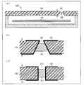
すなわち、図4の(a)およびその拡大図である図4の(b)に示すように、外部から見たときに目立たないよう、筐体103の内側(図中B側)に向けて開いていくように形成された、テーパ状の貫通孔101を有する筐体103において、貫通孔101を注入材102で埋めた場合、筐体103の外側(図中A側)から圧力がかかったときに注入材102を支持することができず、注入材102が筐体103の内側(図中B側)に外れてしまうという問題がある。このことは、図4の(c)に示すように、筐体103が、円筒状の貫通孔111を有する場合も、同様である。そして、注入材102が筐体103の内側(図中B側)に外れてしまうと、防水および防塵性能が劣化する他、注入材102が筐体103内で動き回り、回路基板104等の部品を損傷または破損するおそれがある。そのため、筐体103が有する貫通孔を好適に塞ぐための技術が求められている。
本発明は、上記問題に鑑みてなされたものであり、導電パターンを通過させるための貫通孔を有する筐体において、当該貫通孔を好適に塞ぐための技術を提供することを主たる目的とする。
上記の課題を解決するために、本発明の一態様に係る筐体は、その内部に回路基板を格納するための筐体であって、該筐体の外側および内側に開口する貫通孔と、該筐体の外側の表面から該貫通孔の内壁を通って該筐体の内側の表面に引き廻され、該回路基板に導通される導電パターンと、該貫通孔を塞ぐ栓部材と、を備えており、該貫通孔における該筐体の外側の開口部の方が、該貫通孔における該筐体の内側の開口部よりも大きいことを特徴としている。
本発明の一態様によれば、貫通孔における筐体の外側の開口部の方が、貫通孔における該筐体の内側の開口部よりも大きいため、貫通孔が、栓部材を筐体の内側から支持する形状となっている。これにより、筐体の外側から圧力が掛ったときに栓部材が外れることを防止することができ、貫通孔を好適に塞ぐことができる。
〔実施形態1〕
以下、本発明の実施の形態について、詳細に説明する。
以下、本発明の実施の形態について、詳細に説明する。
(携帯端末20の構成)
図1の(a)は、本発明の実施形態1に係る携帯端末(無線通信装置)20を示す図であり、(b)は、(a)の貫通孔1を拡大した図である。
図1の(a)は、本発明の実施形態1に係る携帯端末(無線通信装置)20を示す図であり、(b)は、(a)の貫通孔1を拡大した図である。
携帯端末20は、筐体3の内部に無線通信のための回路基板4を格納し、回路基板4に実装されるハードウェアおよびソフトウェアにより、携帯端末として機能する。筐体3は、貫通孔1、注入材(栓部材)2および導電パターン5を備えている。導電パターン5は、コネクタ6を介して回路基板4に接続されており、携帯端末20は、導電パターン5をアンテナとして、無線通信する機能を有している。
筐体3は、誘電体からなる構造物であり、例えば、樹脂等によって形成することができる。
また、本明細書において、導電パターンとは、任意の形状に形成された膜状または板状の導電体を意味する。導電パターン5は、筐体3の表面に設けられており、貫通孔1の内壁を通って、筐体3の内側(図中B側)の表面から筐体3の外側(図中A側)の表面に引き廻されている。すなわち、貫通孔1の内壁上に設けられた導電パターン5は、貫通孔1が開口する二面(筐体3の図中A側およびB側の表面)間を導電接続している。
一つの局面において、導電パターン5は、LDS(Laser Direct Structuring)法を用いて形成することができる。すなわち、筐体3を構成する樹脂に有機金属を混合しておき、筐体3上の導電パターン5を形成する領域にレーザ照射することによって、レーザ照射部にメッキを析出させたり、レーザ照射部が微細に荒れることによって、メッキがそのレーザ照射部に結合し、導電パターン5を形成することができる。導電パターン5を構成する物質は特に限定されず、導電性を有する物質(例えば、銅メッキ、ニッケルメッキなどの金属)を用いればよい。なお、LDS法により貫通孔1の内壁に導電パターン5を形成する場合、貫通孔1が傾斜を有するテーパ形状であることが、貫通孔1の内壁にレーザを照射する上で好ましい。
貫通孔1は、筐体3を貫通するように設けられた孔であり、筐体3の外側(図中A側)および内側(図中B側)にそれぞれ付された導電パターン5同士を接続するために、筐体3の外側(図中A側)および内側(図中B側)にそれぞれ開口するように形成されている。図1に示すように、貫通孔1は、貫通孔1における筐体3の外側(図中A側)の開口部の方が、貫通孔1における内側(図中B側)の開口部よりも大きくなるように形成されている。より詳細には、筐体3の外側(図中A側)から内側(図中B側)に向けて先細になる(径が狭まる)テーパ状の形状を有していている。これにより、上述したLDS法等により貫通孔1の内壁に導電パターンをより容易に形成することができる。なお、貫通孔1の各開口部の形状は限定されず、円形の他、例えば、楕円形、多角形(三角形および四角形を含む)、円または楕円と多角形とが複合した形状等が挙げられる。
注入材2は、携帯端末20の筐体3の内側に対する防水および防塵機能を実現するために、貫通孔1を塞ぐように設けられる。注入材2は、注入時には粘性のある液体状またはジェル状であり、貫通孔1内に注入された後、固化(乾燥)するものであり得る。このような注入材2としては、特に限定されないが、例えば、液体糊、樹脂系の粘着剤、接着剤、補強材等が挙げられる。なお、注入材2は、絶縁体であってもよし、導電性を有していてもよい。
なお、貫通孔1が傾斜を有するテーパ形状であることが、貫通孔1内に注入材2を注入する上で好ましい。
(本実施形態の利点)
上述したように、貫通孔1は、貫通孔1における筐体3の外側(図中A側)の開口部の方が、貫通孔1における内側(図中B側)の開口部よりも大きくなるように形成されている。このような構造により、貫通孔1は、注入材2を筐体3の内側(図中B側)から支持することができるため、筐体3の外側(図中A側)から圧力がかかっても、注入材2が外れて筐体3の内部に入ることはない。
上述したように、貫通孔1は、貫通孔1における筐体3の外側(図中A側)の開口部の方が、貫通孔1における内側(図中B側)の開口部よりも大きくなるように形成されている。このような構造により、貫通孔1は、注入材2を筐体3の内側(図中B側)から支持することができるため、筐体3の外側(図中A側)から圧力がかかっても、注入材2が外れて筐体3の内部に入ることはない。
これにより、注入材2が外れ、筐体3の防水および防塵機能が劣化することを防止することができる。また、注入材2が筐体3の内部に入り、回路基板4等の内部の部品を損傷または破損することを防止することができる。また、注入材2として、導電性を有する物質を用いた場合であっても、注入材2が筐体3の内部に入り、回路基板4をショートさせることを防止することができる。
また、図4に示したような構成では、注入材2が外れることを防止し得るように、注入材2と筐体3との間の接着強度を考慮する必要があり、注入材2の材質等について設計制約があるが、本実施形態では、貫通孔1が物理的に注入材2を支持するため、注入材2の材質等についての設計制約が小さくなり、注入材2として、低損失体等の所望の機能を有するもの、コストを低減し得るもの等、用途および仕様に合わせて、様々な物質を使用することができる。
また、図1の(b)に示すように、貫通孔1における筐体3の外側(図中A側)の開口部の方が、貫通孔1における内側(図中B側)の開口部よりも大きいため、貫通孔1における内側(図中B側)の開口部の方が大きい場合に比べて、導電パターン5およびコネクタ6の接点32と、貫通孔中心31との間の距離33を短くすることができる。なぜなら、貫通孔1における筐体3の内側(図中B側)の開口部が大きくなると、貫通孔中心31近くに接点32を設けることができないためである。これにより、筐体3の内側(図中B側)に必要となる導電パターン5の長さを短くすることができる。例えば、接点32から、貫通孔1の反対斜面まで引き廻される導電パターン5の長さを短くすることができる。これにより、導電パターン5(アンテナエレメント)の全長を、所望の使用周波数帯域に対応した長さにする場合に、筐体3の内側(図中B側)に必要となる導電パターン5の長さを短くして、筐体3の外側(図中A側)に配置された導電パターン5(アンテナエレメント)の長さを長くすることができる。これにより、筐体3の外側にアンテナエレメントを配置して、回路基板4等の金属から距離を取ることが出来るため、アンテナ性能を改善することができる。
(変形例)
なお、導電パターン5は、アンテナエレメントとしての用途以外にも様々な用途に用いることができる。例えば、一つの局面において、導電パターン5は、筐体3の内側(図中B側)と外側(図中A側)とを導電接続するために使用することができる。例えば、筐体3の外側(図中A側)に、板金等のグランドを配置し、導電パターン5と導通することにより、板金等のグランドと回路基板4とを導電パターン5を介して電気的に接続することができる。
なお、導電パターン5は、アンテナエレメントとしての用途以外にも様々な用途に用いることができる。例えば、一つの局面において、導電パターン5は、筐体3の内側(図中B側)と外側(図中A側)とを導電接続するために使用することができる。例えば、筐体3の外側(図中A側)に、板金等のグランドを配置し、導電パターン5と導通することにより、板金等のグランドと回路基板4とを導電パターン5を介して電気的に接続することができる。
また、導電パターン5の形成方法はLDS法に限定されるものではない。例えば、導電ペースト、導電インク等を筐体3上に印刷してもよいし、MID(Molded Interconnect Devices)法を用いてもよいし、導電性の薄膜を筐体3に貼付けてもよい。
また、貫通孔1を塞ぐ部材は、貫通孔1に注入される注入材2に限定されず、貫通孔1を塞ぐ栓となる栓部材であればよい。当該栓部材は、例えば、貫通孔1に挿入される弾性体等であり得る。
〔実施形態2〕
本発明の他の実施形態について、図2に基づいて説明すれば、以下のとおりである。なお、説明の便宜上、前記実施形態にて説明した部材と同じ機能を有する部材については、同じ符号を付記し、その説明を省略する。また、実施形態1における変形例は、同様に適用することができる。
本発明の他の実施形態について、図2に基づいて説明すれば、以下のとおりである。なお、説明の便宜上、前記実施形態にて説明した部材と同じ機能を有する部材については、同じ符号を付記し、その説明を省略する。また、実施形態1における変形例は、同様に適用することができる。
図2は、本発明の実施形態2における貫通孔11の周囲を拡大した図である。図2に示すように、貫通孔11は、筐体3の外側(図中A側)から内側(図中B側)に向かって径が狭まるような段差を有し、貫通孔11における筐体3の外側(図中A側)の開口部の方が、貫通孔11における内側(図中B側)の開口部よりも大きくなっている。実施形態2においても、実施形態1と同様、貫通孔11が注入材2を筐体3の内側(図中B側)から支持するため、筐体3の外側(図中A側)から圧力が掛ったときに注入材2が外れて筐体3の内部に入ることを防止することができる。また、貫通孔がテーパ形状を有する場合とは異なり、筐体3の厚さが増しても、貫通孔11における筐体3の外側(図中A側)の開口部の大きさが変わらないという利点がある。
〔実施形態3〕
本発明の他の実施形態について、図3に基づいて説明すれば、以下のとおりである。なお、説明の便宜上、実施形態1にて説明した部材と同じ機能を有する部材については、同じ符号を付記し、その説明を省略する。また、実施形態1における変形例は、同様に適用することができる。
本発明の他の実施形態について、図3に基づいて説明すれば、以下のとおりである。なお、説明の便宜上、実施形態1にて説明した部材と同じ機能を有する部材については、同じ符号を付記し、その説明を省略する。また、実施形態1における変形例は、同様に適用することができる。
図3は、本発明の実施形態3における貫通孔1の周囲を拡大した図である。図3に示すように、貫通孔1の形状は、実施形態1と同様、筐体3の外側(図中A側)に向かって径が大きくなるすり鉢状である。このように、筐体3の外側(図中A側)に向けて貫通孔1が開いているため、筐体3の外側(図中A側)から注入材2を引っ掛ける力が働くと、注入材2が外れてしまうおそれがある。これに対し、実施形態3では、筐体3の外側(図中A側)の表面の少なくとも一部を覆う塗膜7を備えており、塗膜7は、注入材2を覆うように形成されている。塗膜7が固着することによって、注入材2と筐体3とが接着する力に加えて、塗膜7の固着力も加わるので、注入材2をより強固に筐体3に固定することができる。また、塗膜7が注入材2と筐体3との段差を埋めるため、筐体3と注入材2との間の境界を滑らかにし、引っかかりを低減することにより、注入材2が外れることをさらに好適に防止することができる。
また、本実施形態では、塗膜7によって注入材2が外れることをさらに好適に防止することができるため、注入材2の材質等についての設計制約がさらに小さくなり、様々な物質を使用することができる。また、塗膜7により注入材2の腐食から保護することができるため、導電性を有する注入材2等を首尾よく使用することができる。
〔まとめ〕
本発明の態様1に係る筐体は、その内部に回路基板(4)を格納するための筐体(3)であって、該筐体の外側および内側に開口する貫通孔(1)と、該筐体の外側の表面から該貫通孔の内壁を通って該筐体の内側の表面に引き廻され、該回路基板に導通される導電パターン(5)と、該貫通孔を塞ぐ栓部材(注入材2)と、を備えており、該貫通孔における該筐体の外側の開口部の方が、該貫通孔における該筐体の内側の開口部よりも大きいことを特徴としている。
本発明の態様1に係る筐体は、その内部に回路基板(4)を格納するための筐体(3)であって、該筐体の外側および内側に開口する貫通孔(1)と、該筐体の外側の表面から該貫通孔の内壁を通って該筐体の内側の表面に引き廻され、該回路基板に導通される導電パターン(5)と、該貫通孔を塞ぐ栓部材(注入材2)と、を備えており、該貫通孔における該筐体の外側の開口部の方が、該貫通孔における該筐体の内側の開口部よりも大きいことを特徴としている。
上記の構成によれば、貫通孔における筐体の外側の開口部の方が、貫通孔における該筐体の内側の開口部よりも大きいため、貫通孔が、栓部材を筐体の内側から支持する形状となっている。これにより、筐体の外側から圧力が掛ったときに栓部材が外れることを防止することができ、貫通孔を好適に塞ぐことができる。
本発明の態様2に係る筐体では、上記態様1において、上記筐体が格納する回路基板は、無線通信のための回路基板であり、上記導電パターンは、アンテナエレメントであってもよい。
上記の構成によれば、筐体の外側の表面に設けられた導電パターンをアンテナエレメントとして使用することにより、効率良く無線通信を行うことができる。特に、上記の構成によれば、貫通孔における筐体の外側の開口部の方が、貫通孔における筐体の内側の開口部よりも大きいため、筐体の内側の開口部の方が大きい場合に比べて、導電パターンと回路基板との接点を貫通孔の近くに配置することができる。これにより、筐体の外側にアンテナエレメントを配置して、回路基板等の金属から距離を取ることが出来るため、アンテナ性能を改善することができる。
本発明の態様3に係る筐体は、上記態様1または2において、上記貫通孔が、上記筐体の外側から上記筐体の内側に向けて先細になるテーパ状の形状を有していてもよい。
上記の構成によれば、貫通孔内に栓部材をより好適に注入することができる。また、例えば、LDS(Laser Direct Structuring)法等を用いて、貫通孔の内壁に導電パターンをより容易に形成することができる。
本発明の態様4に係る筐体は、上記態様1~3において、上記筐体の外側の表面の少なくとも一部を覆う塗膜を備えており、該塗膜が、上記栓部材を覆っていてもよい。
上記の構成によれば、塗膜が固着することによって、栓部材をより強固に筐体に固定することができるとともに、塗膜によって、筐体と栓部材との間の境界を滑らかにし、引っかかりを低減することにより、栓部材が外れることをさらに好適に防止することができる。
本発明の態様5に係る無線通信装置(携帯端末20)は、上記態様1~4における筐体と、上記回路基板とを備えていることを特徴としている。
上記の構成によれば、上記態様1~4と同等の効果を奏する。
本発明は上述した各実施形態に限定されるものではなく、請求項に示した範囲で種々の変更が可能であり、異なる実施形態にそれぞれ開示された技術的手段を適宜組み合わせて得られる実施形態についても本発明の技術的範囲に含まれる。さらに、各実施形態にそれぞれ開示された技術的手段を組み合わせることにより、新しい技術的特徴を形成することができる。
本発明は、回路基板を格納する筐体を備えた電子機器に幅広く利用することができ、特に、スマートフォン、タブレット端末等の無線通信装置において、好適に利用することができる。
1、11 貫通孔
2 注入材(栓部材)
3 筐体
4 回路基板
5 導電パターン
6 コネクタ
7 塗膜
20 携帯端末(無線通信装置)
2 注入材(栓部材)
3 筐体
4 回路基板
5 導電パターン
6 コネクタ
7 塗膜
20 携帯端末(無線通信装置)
Claims (5)
- その内部に回路基板を格納するための筐体であって、
該筐体の外側および内側に開口する貫通孔と、
該筐体の外側の表面から該貫通孔の内壁を通って該筐体の内側の表面に引き廻され、該回路基板に導通される導電パターンと、
該貫通孔を塞ぐ栓部材と、を備えており、
該貫通孔における該筐体の外側の開口部の方が、該貫通孔における該筐体の内側の開口部よりも大きいことを特徴とする筐体。 - 上記筐体が格納する回路基板は、無線通信のための回路基板であり、
上記導電パターンは、アンテナエレメントであることを特徴とする請求項1に記載の筐体。 - 上記貫通孔が、上記筐体の外側から上記筐体の内側に向けて先細になるテーパ状の形状を有していることを特徴とする請求項1または2に記載の筐体。
- 上記筐体の外側の表面の少なくとも一部を覆う塗膜を備えており、
該塗膜が、上記栓部材を覆っていることを特徴とする請求項1~3の何れか一項に記載の筐体。 - 請求項1~4の何れか一項に記載の筐体と、
上記回路基板とを備えていることを特徴とする無線通信装置。
Priority Applications (1)
| Application Number | Priority Date | Filing Date | Title |
|---|---|---|---|
| US14/434,798 US9848505B2 (en) | 2013-02-08 | 2013-11-25 | Case and wireless communication device |
Applications Claiming Priority (2)
| Application Number | Priority Date | Filing Date | Title |
|---|---|---|---|
| JP2013-023715 | 2013-02-08 | ||
| JP2013023715A JP6234032B2 (ja) | 2013-02-08 | 2013-02-08 | 筐体および無線通信装置 |
Publications (1)
| Publication Number | Publication Date |
|---|---|
| WO2014122838A1 true WO2014122838A1 (ja) | 2014-08-14 |
Family
ID=51299445
Family Applications (1)
| Application Number | Title | Priority Date | Filing Date |
|---|---|---|---|
| PCT/JP2013/081634 Ceased WO2014122838A1 (ja) | 2013-02-08 | 2013-11-25 | 筐体および無線通信装置 |
Country Status (3)
| Country | Link |
|---|---|
| US (1) | US9848505B2 (ja) |
| JP (1) | JP6234032B2 (ja) |
| WO (1) | WO2014122838A1 (ja) |
Cited By (1)
| Publication number | Priority date | Publication date | Assignee | Title |
|---|---|---|---|---|
| JP2019186627A (ja) * | 2018-04-03 | 2019-10-24 | ジャパン・イーエム・ソリューションズ株式会社 | 電子機器 |
Families Citing this family (5)
| Publication number | Priority date | Publication date | Assignee | Title |
|---|---|---|---|---|
| JP6236377B2 (ja) * | 2014-11-26 | 2017-11-22 | 京セラ株式会社 | アンテナ構造体および電子機器 |
| US10361476B2 (en) * | 2015-05-26 | 2019-07-23 | Qualcomm Incorporated | Antenna structures for wireless communications |
| JP2017098472A (ja) | 2015-11-27 | 2017-06-01 | 京セラ株式会社 | 電子機器およびその製造方法 |
| KR102390322B1 (ko) * | 2017-12-19 | 2022-04-26 | 삼성전자주식회사 | 안테나 장치를 포함하는 전자 장치 |
| KR102572820B1 (ko) * | 2018-11-19 | 2023-08-30 | 삼성전자 주식회사 | 혼 구조를 이용한 안테나 및 그것을 포함하는 전자 장치 |
Citations (4)
| Publication number | Priority date | Publication date | Assignee | Title |
|---|---|---|---|---|
| JP2003318501A (ja) * | 2002-04-26 | 2003-11-07 | Nec Kansai Ltd | 配線基板 |
| JP2008305168A (ja) * | 2007-06-07 | 2008-12-18 | Toshiba Corp | 電子機器及びその製造方法 |
| JP2009027019A (ja) * | 2007-07-20 | 2009-02-05 | Toshiba Corp | 電子機器 |
| WO2012086034A1 (ja) * | 2010-12-22 | 2012-06-28 | 磐田電工株式会社 | 電子機器用筐体における表示部構造 |
Family Cites Families (17)
| Publication number | Priority date | Publication date | Assignee | Title |
|---|---|---|---|---|
| JPS6331329Y2 (ja) * | 1979-06-18 | 1988-08-22 | ||
| JPH07220558A (ja) * | 1994-02-04 | 1995-08-18 | Omron Corp | 熱封止構造 |
| US5731629A (en) * | 1995-03-10 | 1998-03-24 | Data-Disk Technology, Inc. | Personal memory devices carried by an individual which can be read and written to |
| JPH10322046A (ja) * | 1997-05-22 | 1998-12-04 | Tokai Rubber Ind Ltd | シール構造 |
| AU2003236055A1 (en) * | 2002-04-11 | 2003-10-20 | Nok Corporation | Sealing structure |
| US20050157480A1 (en) * | 2004-01-16 | 2005-07-21 | Huei-Hsin Sun | Waterproof, vibration-proof, and heat dissipative housing of an electronic element |
| JP4633605B2 (ja) * | 2005-01-31 | 2011-02-16 | 富士通コンポーネント株式会社 | アンテナ装置及び電子装置、並びに、電子カメラ、電子カメラの発光装置、並びに、周辺装置 |
| JP4754601B2 (ja) * | 2005-01-31 | 2011-08-24 | 富士通コンポーネント株式会社 | アンテナ装置 |
| JP4835232B2 (ja) * | 2006-03-31 | 2011-12-14 | 株式会社ジェイテクト | 電子制御装置 |
| JP4102411B2 (ja) | 2006-04-13 | 2008-06-18 | 株式会社東芝 | 移動通信端末 |
| JP4711978B2 (ja) * | 2007-01-25 | 2011-06-29 | 株式会社東芝 | 電子機器 |
| JP5274801B2 (ja) * | 2007-08-30 | 2013-08-28 | 京セラ株式会社 | 携帯端末 |
| JP2009064916A (ja) * | 2007-09-05 | 2009-03-26 | Kokusan Denki Co Ltd | 電子ユニット及びその製造方法 |
| TWI342180B (en) * | 2007-10-09 | 2011-05-11 | Asustek Comp Inc | Housing structure |
| KR100961137B1 (ko) * | 2008-08-05 | 2010-06-09 | 삼성전기주식회사 | 이동통신 단말기 케이스 및 그 제조방법 |
| US8264837B2 (en) * | 2010-04-19 | 2012-09-11 | Apple Inc. | Systems and methods for cover assembly retention of a portable electronic device |
| CN105319392A (zh) * | 2014-07-31 | 2016-02-10 | 精工爱普生株式会社 | 物理量传感器及其制造方法、电子设备及移动体 |
-
2013
- 2013-02-08 JP JP2013023715A patent/JP6234032B2/ja not_active Expired - Fee Related
- 2013-11-25 US US14/434,798 patent/US9848505B2/en not_active Expired - Fee Related
- 2013-11-25 WO PCT/JP2013/081634 patent/WO2014122838A1/ja not_active Ceased
Patent Citations (4)
| Publication number | Priority date | Publication date | Assignee | Title |
|---|---|---|---|---|
| JP2003318501A (ja) * | 2002-04-26 | 2003-11-07 | Nec Kansai Ltd | 配線基板 |
| JP2008305168A (ja) * | 2007-06-07 | 2008-12-18 | Toshiba Corp | 電子機器及びその製造方法 |
| JP2009027019A (ja) * | 2007-07-20 | 2009-02-05 | Toshiba Corp | 電子機器 |
| WO2012086034A1 (ja) * | 2010-12-22 | 2012-06-28 | 磐田電工株式会社 | 電子機器用筐体における表示部構造 |
Cited By (1)
| Publication number | Priority date | Publication date | Assignee | Title |
|---|---|---|---|---|
| JP2019186627A (ja) * | 2018-04-03 | 2019-10-24 | ジャパン・イーエム・ソリューションズ株式会社 | 電子機器 |
Also Published As
| Publication number | Publication date |
|---|---|
| US9848505B2 (en) | 2017-12-19 |
| JP2014155064A (ja) | 2014-08-25 |
| JP6234032B2 (ja) | 2017-11-22 |
| US20150289401A1 (en) | 2015-10-08 |
Similar Documents
| Publication | Publication Date | Title |
|---|---|---|
| JP6234032B2 (ja) | 筐体および無線通信装置 | |
| US9462094B2 (en) | Device housing and portable electronic device using same | |
| CN206727226U (zh) | 天线装置以及电子设备 | |
| US9323357B2 (en) | Electronic device with stylus pen having FM antenna functionality | |
| JP5823774B2 (ja) | 導電部材およびこれを備える電子機器 | |
| JP2013214961A (ja) | アンテナ部材 | |
| US20150207208A1 (en) | Electronic device housing and method for making same | |
| JP5868658B2 (ja) | 構造体 | |
| KR102887016B1 (ko) | 전자기 차폐 캡, 전기 시스템 및 전자기 차폐 캡을 형성하는 방법 | |
| KR101598293B1 (ko) | 안테나 패턴 프레임 및 이를 포함하는 전자장치 | |
| CN103928753B (zh) | 一种手机及其天线 | |
| KR101053296B1 (ko) | 전자파 차폐 기능을 갖는 전자 장치 | |
| KR101387618B1 (ko) | 인서트 안테나 모듈 및 그 제조방법 | |
| JP5774508B2 (ja) | アンテナ構造体および無線装置 | |
| JP5666399B2 (ja) | 構造物の製造方法 | |
| JP6112263B2 (ja) | 電子機器 | |
| KR101632205B1 (ko) | 갈바닉 내부식특성을 향상시킨 이동통신 단말기용 안테나의 제작방법, 이에 의해 제조된 이동통신 단말기용 케이스 및 이를 갖는 이동통신 단말기 | |
| KR102879508B1 (ko) | 고주파 대역의 신호를 전달하는 인쇄 회로 기판 및 그것을 포함하는 전자 장치 | |
| CN205249346U (zh) | 摄像头模组及移动终端 | |
| CN106060193B (zh) | 一种移动终端 | |
| US20090040128A1 (en) | Mobile apparatus and method of manufacturing the same | |
| JP2013069781A (ja) | 電子装置 | |
| US10361486B2 (en) | External antenna and method for manufacturing the same | |
| CN102723632A (zh) | 一种防渗电连接端子及其金属端子、电子装置 | |
| KR101597719B1 (ko) | 방수성능이 향상된 안테나 패턴 형성 하우징 |
Legal Events
| Date | Code | Title | Description |
|---|---|---|---|
| 121 | Ep: the epo has been informed by wipo that ep was designated in this application |
Ref document number: 13874626 Country of ref document: EP Kind code of ref document: A1 |
|
| WWE | Wipo information: entry into national phase |
Ref document number: 14434798 Country of ref document: US |
|
| NENP | Non-entry into the national phase |
Ref country code: DE |
|
| 122 | Ep: pct application non-entry in european phase |
Ref document number: 13874626 Country of ref document: EP Kind code of ref document: A1 |