WO2014109111A1 - 高周波スイッチモジュール - Google Patents
高周波スイッチモジュール Download PDFInfo
- Publication number
- WO2014109111A1 WO2014109111A1 PCT/JP2013/079074 JP2013079074W WO2014109111A1 WO 2014109111 A1 WO2014109111 A1 WO 2014109111A1 JP 2013079074 W JP2013079074 W JP 2013079074W WO 2014109111 A1 WO2014109111 A1 WO 2014109111A1
- Authority
- WO
- WIPO (PCT)
- Prior art keywords
- circuit
- frequency
- filter
- switch module
- band
- Prior art date
- Legal status (The legal status is an assumption and is not a legal conclusion. Google has not performed a legal analysis and makes no representation as to the accuracy of the status listed.)
- Ceased
Links
Images







Classifications
-
- H—ELECTRICITY
- H03—ELECTRONIC CIRCUITRY
- H03H—IMPEDANCE NETWORKS, e.g. RESONANT CIRCUITS; RESONATORS
- H03H7/00—Multiple-port networks comprising only passive electrical elements as network components
- H03H7/01—Frequency selective two-port networks
- H03H7/0115—Frequency selective two-port networks comprising only inductors and capacitors
-
- H—ELECTRICITY
- H03—ELECTRONIC CIRCUITRY
- H03H—IMPEDANCE NETWORKS, e.g. RESONANT CIRCUITS; RESONATORS
- H03H7/00—Multiple-port networks comprising only passive electrical elements as network components
- H03H7/46—Networks for connecting several sources or loads, working on different frequencies or frequency bands, to a common load or source
- H03H7/463—Duplexers
-
- H—ELECTRICITY
- H04—ELECTRIC COMMUNICATION TECHNIQUE
- H04B—TRANSMISSION
- H04B1/00—Details of transmission systems, not covered by a single one of groups H04B3/00 - H04B13/00; Details of transmission systems not characterised by the medium used for transmission
- H04B1/005—Details of transmission systems, not covered by a single one of groups H04B3/00 - H04B13/00; Details of transmission systems not characterised by the medium used for transmission adapting radio receivers, transmitters andtransceivers for operation on two or more bands, i.e. frequency ranges
- H04B1/0053—Details of transmission systems, not covered by a single one of groups H04B3/00 - H04B13/00; Details of transmission systems not characterised by the medium used for transmission adapting radio receivers, transmitters andtransceivers for operation on two or more bands, i.e. frequency ranges with common antenna for more than one band
- H04B1/0057—Details of transmission systems, not covered by a single one of groups H04B3/00 - H04B13/00; Details of transmission systems not characterised by the medium used for transmission adapting radio receivers, transmitters andtransceivers for operation on two or more bands, i.e. frequency ranges with common antenna for more than one band using diplexing or multiplexing filters for selecting the desired band
-
- H—ELECTRICITY
- H04—ELECTRIC COMMUNICATION TECHNIQUE
- H04B—TRANSMISSION
- H04B1/00—Details of transmission systems, not covered by a single one of groups H04B3/00 - H04B13/00; Details of transmission systems not characterised by the medium used for transmission
- H04B1/02—Transmitters
- H04B1/04—Circuits
- H04B1/0458—Arrangements for matching and coupling between power amplifier and antenna or between amplifying stages
-
- H—ELECTRICITY
- H04—ELECTRIC COMMUNICATION TECHNIQUE
- H04B—TRANSMISSION
- H04B1/00—Details of transmission systems, not covered by a single one of groups H04B3/00 - H04B13/00; Details of transmission systems not characterised by the medium used for transmission
- H04B1/06—Receivers
- H04B1/16—Circuits
- H04B1/18—Input circuits, e.g. for coupling to an antenna or a transmission line
-
- H—ELECTRICITY
- H04—ELECTRIC COMMUNICATION TECHNIQUE
- H04B—TRANSMISSION
- H04B1/00—Details of transmission systems, not covered by a single one of groups H04B3/00 - H04B13/00; Details of transmission systems not characterised by the medium used for transmission
- H04B1/38—Transceivers, i.e. devices in which transmitter and receiver form a structural unit and in which at least one part is used for functions of transmitting and receiving
- H04B1/40—Circuits
- H04B1/44—Transmit/receive switching
- H04B1/48—Transmit/receive switching in circuits for connecting transmitter and receiver to a common transmission path, e.g. by energy of transmitter
-
- H—ELECTRICITY
- H03—ELECTRONIC CIRCUITRY
- H03H—IMPEDANCE NETWORKS, e.g. RESONANT CIRCUITS; RESONATORS
- H03H1/00—Constructional details of impedance networks whose electrical mode of operation is not specified or applicable to more than one type of network
- H03H2001/0021—Constructional details
- H03H2001/0085—Multilayer, e.g. LTCC, HTCC, green sheets
-
- H—ELECTRICITY
- H03—ELECTRONIC CIRCUITRY
- H03H—IMPEDANCE NETWORKS, e.g. RESONANT CIRCUITS; RESONATORS
- H03H7/00—Multiple-port networks comprising only passive electrical elements as network components
- H03H7/01—Frequency selective two-port networks
- H03H2007/013—Notch or bandstop filters
-
- H—ELECTRICITY
- H03—ELECTRONIC CIRCUITRY
- H03H—IMPEDANCE NETWORKS, e.g. RESONANT CIRCUITS; RESONATORS
- H03H7/00—Multiple-port networks comprising only passive electrical elements as network components
- H03H7/18—Networks for phase shifting
- H03H7/19—Two-port phase shifters providing a predetermined phase shift, e.g. "all-pass" filters
-
- H—ELECTRICITY
- H03—ELECTRONIC CIRCUITRY
- H03H—IMPEDANCE NETWORKS, e.g. RESONANT CIRCUITS; RESONATORS
- H03H7/00—Multiple-port networks comprising only passive electrical elements as network components
- H03H7/18—Networks for phase shifting
- H03H7/21—Networks for phase shifting providing two or more phase shifted output signals, e.g. n-phase output
-
- H—ELECTRICITY
- H04—ELECTRIC COMMUNICATION TECHNIQUE
- H04B—TRANSMISSION
- H04B1/00—Details of transmission systems, not covered by a single one of groups H04B3/00 - H04B13/00; Details of transmission systems not characterised by the medium used for transmission
- H04B1/38—Transceivers, i.e. devices in which transmitter and receiver form a structural unit and in which at least one part is used for functions of transmitting and receiving
- H04B1/40—Circuits
- H04B1/44—Transmit/receive switching
- H04B1/48—Transmit/receive switching in circuits for connecting transmitter and receiver to a common transmission path, e.g. by energy of transmitter
- H04B2001/485—Transmit/receive switching in circuits for connecting transmitter and receiver to a common transmission path, e.g. by energy of transmitter inhibiting unwanted transmission
Definitions
- the present invention relates to a high-frequency switch module that transmits and receives a plurality of types of high-frequency signals by switching and connecting a common terminal to a plurality of individual terminals using a semiconductor switch.
- a switch IC having one common terminal and a plurality of individual terminals may be used.
- the switch IC includes a plurality of FETs (field effect transistors), and a common terminal is connected to any one individual terminal by turning on / off these FETs.
- a high-power high-frequency signal for example, a transmission signal
- a harmonic signal due to distortion is generated.
- Transmission of such a harmonic signal from the common terminal to the outside via the antenna causes various problems such as radio wave interference. That is, the harmonic signal caused by such distortion causes the out-of-band characteristics of the high-frequency switch module to deteriorate.
- the high-frequency circuit described in Patent Document 1 includes an LC series resonator that reflects the harmonic signal generated by the switch IC and output to the individual terminal.
- the LC series resonator is connected between a signal transmission line connecting the individual terminal of the switch IC and the transmission circuit and the ground.
- the harmonic signal output from the individual terminal is reflected at the connection point of the LC series resonator, returns to the switch IC, and is transmitted to the common terminal.
- the harmonic signal output from the common terminal and the LC series resonator from the individual terminal are set.
- the phase of the harmonic signal reflected from the connection point and output to the common terminal is reversed. Thereby, the harmonic signal transmitted from the antenna is suppressed.
- the phase of the harmonic signal from the individual terminal is adjusted by the length of the signal transmission line which is a distributed constant line.
- the signal transmission line must be lengthened.
- the shape of the laminated body forming the signal transmission line becomes large.
- An object of the present invention is to provide a high-frequency switch module that is excellent in harmonic distortion characteristics and out-of-band characteristics without increasing the size.
- the present invention relates to a high frequency switch module including a switch IC having a common terminal and a plurality of individual terminals, and switching and connecting the plurality of individual terminals to the common terminal by turning on and off the semiconductor switch element. Harmonic signals are output from the common terminal and individual terminals of the switch IC of the high-frequency switch module.
- a high frequency switch module is connected between a first individual terminal of a plurality of individual terminals and a first external connection terminal to which a high frequency signal is input from the outside, and a filter circuit that attenuates harmonic components of the high frequency signal Is provided.
- the high frequency switch module includes a phase adjustment circuit that is connected between the filter circuit and the first individual terminal and includes an inductor and a capacitor. The phase adjustment circuit is configured so that the amplitude of the harmonic signal output from the common terminal and the amplitude of the harmonic signal output from the first individual terminal and reflected by the filter circuit and returning to the first individual terminal cancel each other. And the capacitor element values are determined.
- the harmonic signal output from the first individual terminal is reflected by the filter circuit via the phase adjustment circuit including the inductor and the capacitor, and is output to the common terminal via the phase adjustment circuit and the switch IC.
- the phase adjustment circuit is comprised combining the inductor and the capacitor. Therefore, compared to a conventional phase adjustment circuit using a distributed constant line, the degree of freedom in shape for obtaining a desired phase adjustment amount is improved, the size is easily reduced, and the harmonic distortion characteristics and the out-of-band characteristics are easily improved.
- the inductor and the capacitor have element values such that the phase difference between the harmonic signal from the common terminal and the harmonic signal from the first individual terminal is between 90 ° and 270 °. Is preferably determined.
- the harmonic signal from the common terminal and the harmonic signal from the first individual terminal at least cancel each other, and the level of the harmonic signal output from the common terminal can be suppressed.
- the element values of the inductor and the capacitor are determined so that the phase difference between the harmonic signal from the common terminal and the harmonic signal from the first individual terminal is 180 °. Is preferred.
- phase adjustment circuit of the high frequency switch module of the present invention is preferably a low pass filter that makes the frequency band of the harmonic signal within the pass band.
- the phase adjustment circuit adjusts the phase of the harmonic signal for cancellation, and further uses a higher-order harmonic signal (for example, the above-described harmonic signal is a high-frequency signal input from the filter circuit side). If it is a second-order harmonic signal, a third-order or higher-order harmonic signal) can be attenuated.
- a higher-order harmonic signal for example, the above-described harmonic signal is a high-frequency signal input from the filter circuit side. If it is a second-order harmonic signal, a third-order or higher-order harmonic signal) can be attenuated.
- phase adjustment circuit of the high-frequency switch module of the present invention may be a high-pass filter that makes the frequency band of the high-frequency signal within the pass band.
- the phase adjustment circuit can suppress the static signal input from the common terminal side of the switch IC together with the phase adjustment of the canceling harmonic signal.
- the ESD effect of a filter circuit increases and the ESD effect of a high frequency switch module improves.
- the filter circuit of the high frequency switch module of the present invention is a notch filter in which the frequency of the harmonic signal substantially matches the attenuation pole frequency.
- the high frequency switch module of the present invention preferably has the following configuration.
- the filter circuit includes an LC parallel resonant circuit in which a filter capacitor and a filter inductor are connected in parallel.
- the LC parallel resonance circuit is connected between the first external connection terminal and the phase adjustment circuit.
- the transmission characteristics of the harmonic signal outside the frequency band are good, and the transmission / reception characteristics of the high-frequency switch module can be improved.
- the filter circuit includes an LC series resonance circuit in which a filter capacitor and a filter inductor are connected in series.
- the LC series resonance circuit is connected between a connection line between the first external connection terminal and the phase adjustment circuit and the ground.
- the filter circuit may be a band pass filter having a frequency band of a high frequency signal within a pass band.
- the frequency of the harmonic signal is within the attenuation band of the band pass filter. Since the band pass filter has a large attenuation amount outside the pass band, that is, the reflection amount, the level of the harmonic signal reflected by the filter circuit is unlikely to decrease.
- the band pass filter may be one filter constituting a duplexer.
- the duplexer when the duplexer is connected to the first external connection terminal, it is not necessary to provide a filter circuit separately from the duplexer, and the high-frequency switch module can be made small.
- the high-frequency switch module of the present invention preferably has the following configuration.
- the above-described switch IC of the high-frequency switch module is a low-band switch IC.
- the high frequency switch module includes a high-band second switch IC, a connection terminal to the antenna, a low-band side terminal connected to the common terminal of the switch IC, and a high-band connected to the common terminal of the second switch IC.
- An antenna-side demultiplexer that includes a side terminal and demultiplexes a low-band high-frequency signal and a high-band high-frequency signal. The high-frequency signal input to the first individual terminal and the second high-frequency signal transmitted through the second switch circuit are simultaneously communicated at least temporarily.
- the high frequency switch module of the present invention may have the following configuration.
- a plurality of line conductors and a selection member are provided between the filter circuit and the phase adjustment circuit.
- the plurality of line conductors are connected to the filter circuit and have different lengths.
- the selection member selects and connects the plurality of line conductors to the phase adjustment circuit.
- the high frequency switch module of the present invention may have the following configuration.
- a plurality of line conductors and a selection member are provided between the phase adjustment circuit and the first individual terminal.
- the plurality of line conductors are connected to the phase adjustment circuit and have different lengths.
- the selection member selects and connects the plurality of line conductors to the first individual terminal.
- these open stubs enable further phase adjustment to the harmonic signal. And since the shape of an open stub changes with line conductors to select, a different phase adjustment amount can be selected and it is easy to select a suitable phase adjustment amount suitably.
- the high-frequency switch module of the present invention preferably has the following configuration.
- the high-frequency switch module is formed by a laminated body formed by laminating a plurality of dielectric layers on which conductor patterns are formed.
- the inductor of the phase adjustment circuit is a mounted inductor element that is mounted on the multilayer body.
- the capacitor of the phase adjustment circuit is a mounted capacitor element mounted on the multilayer body.
- phase adjustment circuit without depending on the phase adjustment amount.
- phase adjustment amount can be changed by simply replacing each mounted element. Thereby, a suitable phase adjustment amount can be easily realized and the size can be reduced.
- the high frequency switch module of the present invention preferably has the following configuration.
- the inductor of the filter circuit is a mounting type inductor element mounted on the multilayer body.
- the capacitor of the filter circuit is a mounted capacitor element mounted on the multilayer body.
- a high-frequency switch module excellent in harmonic distortion characteristics and out-of-band characteristics can be realized in a small size and easily.
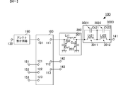
- FIG. 1 is a circuit diagram of a high-frequency switch module according to the first embodiment of the present invention.
- a switch IC having one common terminal and three individual terminals will be described as an example.
- the number of individual terminals is not limited to this. Also good.
- the high frequency switch module 10 includes a switch IC 100, a phase adjustment circuit 200, a filter 300, and an antenna matching circuit 190.
- the high frequency switch module 10 includes external connection terminals 130, 141, 142, 143, 151, 152, and 153.
- the external connection terminal 141 corresponds to the “first external connection terminal” of the present invention.
- the external connection terminal 130 is connected to an antenna ANT disposed outside the high frequency switch module 10.
- the switch IC 100 includes a common terminal 101, individual terminals 111, 112, 113, and drive control terminals 121, 122, 123.
- the individual terminal 111 corresponds to the “first individual terminal” of the present invention.
- the switch IC 100 switches and connects the common terminal 101 to any one of the individual terminals 111, 112, and 113 based on the drive voltage and control signal input to the drive control terminals 121, 122, and 123. More specifically, the switch IC 100 has a structure in which a semiconductor switch such as an FET (field effect transistor) is connected between the common terminal 101 and each individual terminal 111, 112, 113.
- FET field effect transistor
- the switch IC 100 supplies power to the semiconductor switch with a driving voltage, and switches between a semiconductor switch to be turned on and a semiconductor switch to be turned off according to a control signal.
- the switch IC 100 connects the common terminal 101 to any one of the individual terminals 111, 112, and 113 by such on / off control of each semiconductor switch.
- the antenna matching circuit 190 is connected between the common terminal 101 and the external connection terminal 130. Although not shown, the antenna matching circuit 190 is connected to, for example, a series inductor, a capacitor connecting the series inductor and the external connection terminal 130 to the ground, and connecting the series inductor and the common terminal 101 to the ground. Consists of inductors and the like.
- the drive control terminals 121, 122, 123 are connected to the external connection terminals 151, 152, 153, respectively. Drive voltages and control signals are supplied from these external connection terminals 151, 152, and 153.
- the individual terminal 111 is connected to the external connection terminal 141 via the phase adjustment circuit 200 and the filter circuit 300.
- the individual terminals 112 and 113 are connected to external connection terminals 142 and 143, respectively.
- a circuit element such as a filter may be connected between the individual terminals and the external connection terminals.
- the phase adjustment circuit 200 is connected between the individual terminal 111 and the filter circuit 300.
- the phase adjustment circuit 200 includes an inductor 201 and capacitors 202 and 203.
- the inductor 201 is connected in series between the individual terminal 111 and the filter circuit 300.
- the individual terminal 111 side of the inductor 201 is connected to the ground via the capacitor 202.
- the filter circuit 300 side of the inductor 201 is connected to the ground via the capacitor 203.
- the inductance Lt1 of the inductor 201, the capacitance Cu1 of the capacitor 202, and the capacitance Cu2 of the capacitor 203 are set based on the phase shift condition of the second harmonic signal described later.
- the filter circuit 300 includes a filter inductor 301 and a filter capacitor 302.
- the filter inductor 301 is connected between the phase adjustment circuit 200 and the external connection terminal 141.
- the filter capacitor 302 is connected in parallel to the filter inductor 301.
- the filter circuit 300 includes an LC parallel resonance circuit of the filter inductor 301 and the filter capacitor 302. With such a circuit configuration, the filter circuit 300 functions as an LC parallel resonance type notch filter.
- the element value (inductance) Lt2 of the filter inductor 301 and the element value (capacitance) Ct2 of the filter capacitor 302 are the attenuation poles of the notch filter of the frequency of the second harmonic signal of the high frequency signal input from the external connection terminal 141. It is set to match or substantially match the frequency.
- FIG. 2 is a diagram illustrating a transmission state of the high frequency signal when a high frequency signal (high power) is input from the external connection terminal.
- the “high power” in the present invention indicates a power level at which a distorted harmonic signal is generated from the switch IC 100 when a high frequency signal is input to the switch IC 100 used in the high frequency switch module 10.
- FIG. 3 is a diagram illustrating a transmission state of a second harmonic signal of a high frequency signal and a transmission state of a distorted second harmonic signal. 2 and 3 show a state where the individual terminal 111 and the common terminal 101 of the switch IC 100 are electrically connected.
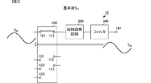
- the high frequency signal (fundamental wave) S f0 having the fundamental frequency input from the external connection terminal 141 is input to the individual terminal 111 of the switch IC 100 via the filter circuit 300 and the phase adjustment circuit 200.
- the high frequency signal S f0 input to the individual terminal 111 of the switch IC 100 is output from the common terminal 101.
- the second harmonic signal S 2f0 of the high frequency signal input from the external connection terminal 141 is attenuated by the filter circuit 300.
- the input second harmonic signal S 2f0 is not transmitted to the phase adjustment circuit 200 and the switch IC 100, and is not output from the common terminal 101 of the switch IC 100.
- the semiconductor switch When the high-frequency signal S f0 having the fundamental frequency is input to the switch IC 100, the semiconductor switch is distorted and a distorted harmonic signal is generated when the high-frequency signal S f0 is high power. Note that most of the power of the distortion harmonic signal is the second harmonic signal SD 2f0 .
- the distorted second harmonic signal SD 2f0 is output to the common terminal 101 and the individual terminal 111.
- the distorted second harmonic signal SD 2f0 output to the individual terminal 111 is transmitted to the filter circuit 300 via the phase adjustment circuit 200. Since the frequency of the second harmonic signal matches the attenuation pole frequency in the filter circuit 300, the distorted second harmonic signal SD2f0 is reflected by the filter circuit 300. The reflected second harmonic signal SDR 2 f 0 is transmitted through the phase adjustment circuit 200 and input to the individual terminal 111. The reflected second harmonic signal SDR 2 f 0 is transmitted from the individual terminal 111 to the common terminal 101.
- phase distortion second harmonic signal SDc 2f0 and phase of the reflected second harmonic signal SDR 2f0 at the common terminal 101 are opposite phases, the inductance of the inductor 201 of the phase adjustment circuit 200 Lt1, the capacitor The capacitance Cu1 of 202 and the capacitance Cu2 of the capacitor 203 are determined.
- the distorted second harmonic signal output from the individual terminal 111 is reflected by the filter circuit 300 and returns to the switch IC 100, and the phase of the reflected second harmonic signal SDR 2f0 at the common terminal 101 is the same as that at the common terminal 101.
- the distortion second harmonic signal SDc 2f0 and reflected second harmonic signal SDR 2f0 at the common terminal 101 is canceled out, resulting in a common
- the second harmonic signal is not output from the terminal 101.
- the secondary harmonic signal is not output to the external connection terminal 130 (antenna ANT) side, and the harmonic distortion characteristics and the out-of-band characteristics of the high-frequency switch module 10 are improved.
- the harmonic distortion characteristic is a characteristic that becomes so good that a harmonic signal having a fundamental frequency as a frequency of a high-frequency signal to be transmitted / received is hardly output to the outside.
- the out-of-band characteristic is a characteristic that is favorable when a large amount of attenuation is obtained in a frequency band other than the frequency band for transmission and reception.
- phase adjustment circuit 200 is configured by the inductor 201 and the capacitors 202 and 203, the secondary that returns to the common terminal 101 rather than the configuration of the microstrip line that is a distributed constant line. Easy to adjust the phase of the harmonic signal. Therefore, as compared with a conventional phase adjustment circuit using distributed constant lines, the degree of freedom in shape for obtaining a desired phase adjustment amount is improved, and downsizing can be realized more easily.
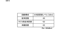
- FIG. 4 shows the result of simulating the second harmonic level in the antenna ANT in the configuration of this embodiment and the conventional configuration.
- FIG. 4 also shows a configuration in which the shape of the FET of the switch IC is doubled in the conventional configuration.
- the level of the input high-frequency signal is +26 [dBm].
- the second harmonic level which was ⁇ 80 [dBm] in the conventional configuration, decreases to ⁇ 95 [dBm] in the configuration of the present embodiment.
- the output of the harmonic signal can be suppressed by increasing the shape of the FET of the switch IC. Therefore, a simulation is also performed for a configuration in which the shape of the conventional switch IC is doubled. As a result, the configuration in which the FET shape of the switch IC is doubled in the conventional configuration is ⁇ 83 [dBm], and therefore the configuration of the present embodiment has a lower second harmonic level than this configuration. Can do.
- the phase adjustment circuit 200 is a ⁇ -type low-pass filter (low-pass filter).
- the inductance Lt1 of the inductor 201, the capacitance Cu1 of the capacitor 202, and the capacitance Cu2 of the capacitor 203 are adjusted so that the frequency of the second harmonic signal is within the pass frequency band, and the frequency band of the third harmonic signal is the attenuation band.
- a low-pass filter is set so that
- the signal level of the second harmonic signal reflected by the filter circuit 300 and returned to the switch IC 100 is hardly lowered. Therefore, the cancellation effect at the common terminal 101 can be improved. As a result, the second harmonic signal output from the common terminal 101 can be more significantly suppressed, and the harmonic distortion characteristics and out-of-band characteristics of the high-frequency switch module 10 can be further improved.
- the filter circuit 300 since the third-order or higher harmonic signal that has passed through the filter circuit 300 is attenuated by the phase adjustment circuit 200, the second-order or higher harmonic signal output from the common terminal 101 can be significantly suppressed. As a result, the harmonic distortion characteristics and the out-of-band characteristics of the high-frequency switch module 10 can be further improved.
- the high-frequency switch module 10 as described above is realized by a laminated body in which a plurality of dielectric layers are laminated.
- a conductor pattern for realizing the circuit pattern of the high-frequency switch module 10 is formed on the predetermined dielectric layer.
- a mounting circuit element is mounted on the top surface of the multilayer body, and a mounting land for realizing an external connection terminal is formed on the bottom surface of the multilayer body.
- FIG. 5 is a stacking diagram of a high-frequency switch module that is an aspect of the present embodiment.
- (circle) described in each dielectric material layer of FIG. 5 shows the conductive via which penetrates a dielectric material layer in the thickness direction.
- FIG. 6 is a circuit diagram of the high-frequency module realized by the pattern of the stacked diagram of FIG.
- phase adjustment circuit 200 and the filter circuit 300 are the same as those of the high-frequency switch module 10 described above.
- the high-frequency switch module 10R includes external connection terminals 130, 141-149, 151-155.
- the switch IC 100R includes one common terminal 101, nine individual terminals 111-119, and five drive control terminals 121-125.
- the common terminal 101 is connected to one of the individual terminals 111 to 119 by a drive voltage and a control signal supplied to the drive control terminals 121 to 125.
- the antenna matching inductor 191 is connected between the common terminal 101 and the external connection terminal 130.
- the antenna matching circuit 190 includes antenna matching inductors 191 and 192 and an antenna matching capacitor 193.
- the antenna matching inductor 191 is connected between the common terminal 101 and the external connection terminal 130.
- the common terminal 101 side of the antenna matching inductor 191 is connected to the ground via the antenna matching inductor 192.
- the external connection terminal 130 side of the antenna matching inductor 191 is connected to the ground via the antenna matching capacitor 193.
- the phase adjustment circuit 200 and the filter circuit 300 are connected between the individual terminal 111 and the external connection terminal 141.
- a low-pass filter 400 is connected between the individual terminal 112 and the external connection terminal 142.
- the low-pass filter 400 includes LPF inductors 401 and 402 and LPF capacitors 411, 412, 421, 422 and 423.
- the LPF inductors 401 and 402 are connected in series between the individual terminal 112 and the external connection terminal 142.
- the LPF capacitor 411 is connected in parallel to the LPF inductor 401.
- the LPF capacitor 412 is connected in parallel to the LPF inductor 402.
- the individual terminal 112 side of the LPF inductor 401 is connected to the ground via the LPF capacitor 421.
- the connection point of the LPF inductors 401 and 402 is connected to the ground via the LPF capacitor 422.
- the external connection terminal 142 side of the LPF inductor 402 is connected to the ground via the LPF capacitor 423.
- the low-pass filter 400 includes the LPF inductors 401 and 402 and the LPF so that the frequency band of the high-frequency signal input to the external connection terminal 142 is in the pass band and the second harmonic frequency or higher is in the attenuation band.
- the element values of the capacitors 411, 412, 421, 422, and 423 are determined.
- a low-pass filter 500 is connected between the individual terminal 113 and the external connection terminal 143.
- the low-pass filter 500 includes LPF inductors 501 and 502 and LPF capacitors 511 and 522.
- the LPF capacitor 511 is connected in parallel to the LPF inductor 501.
- the connection point of the LPF inductors 501 and 502 is connected to the ground via the LPF capacitor 522.
- the low-pass filter 500 includes the LPF inductors 501 and 502 and the LPF so that the frequency band of the high-frequency signal input to the external connection terminal 143 is within the pass band and the second harmonic frequency or higher is the attenuation band. Element values of the capacitors 511, 522 for use are determined.
- the individual terminals 114-119 are connected to external connection terminals 144-149, respectively.
- the drive control terminals 121-125 are connected to the external connection terminals 151-155, respectively.
- Such a high-frequency switch module 10R is realized by a laminated body in which 14 layers from the dielectric layer Ray1 to the dielectric layer Ray14 are laminated as shown in FIG.
- the dielectric layer Ray1 is the uppermost layer of the multilayer body
- the dielectric layer Ray14 is the lowermost layer of the multilayer body.
- the conductor pattern is formed on the upper layer side
- the conductor pattern is formed on the lower layer side.
- the switch IC 100 On the top surface (top surface of the multilayer body) of the dielectric layer Ray1 which is the top layer (first layer), the switch IC 100, the inductor 201, the capacitors 202 and 203, the filter inductor 301, the filter capacitor 302, and the antenna matching Inductors 191, 192 and an antenna matching capacitor 193 are mounted. These circuit elements are mounted circuit elements, and are mounted on element lands formed on the top surface. Inductor 201, capacitors 202 and 203, filter inductor 301, and filter capacitor 302 are spaced apart from antenna matching inductors 191 and 192 and antenna matching capacitor 193 with switch IC 100 interposed therebetween.
- the inductor 201 and capacitors 202 and 203 constituting the phase adjustment circuit 200 are mounted close to each other so as to be aligned with each other. Further, the filter inductor 301 and the filter capacitor 302 are mounted in close proximity so as to be aligned with each other, and are also mounted in close proximity so as to be aligned with the inductor 201 and the capacitors 202 and 203. With such a configuration, the conductor pattern connecting the circuit elements of the phase adjustment circuit 200 can be shortened, and the amount of phase shift due to this conductor pattern can be minimized. Also, the conductor pattern connecting the phase adjustment circuit 200 and the filter circuit 300 can be shortened, and the amount of phase shift due to this conductor pattern can be minimized. Thereby, the phase shift amount of the second harmonic signal returning to the switch IC 100 can be accurately set by the inductor 201 and the capacitors 202 and 203.
- a conductor pattern for routing is appropriately formed on the dielectric layer Ray2 as the second layer and the dielectric layer Ray3 as the third layer. Conductive patterns connecting the switch IC 100, the inductor 201, the capacitors 202 and 203, the filter inductor 301, and the filter capacitor 302 are formed in these dielectric layers. Thereby, the phase shift amount of the second harmonic signal returning to the switch IC 100 can be set with higher accuracy by the inductor 201 and the capacitors 202 and 203.
- the interior ground conductor PtGND1 is formed on substantially the entire surface of the fourth dielectric layer Ray4.
- a conductor pattern for routing is appropriately formed on the dielectric layer Ray5 which is the fifth layer.
- an interior ground conductor PtGND2 and a rectangular conductor for the capacitor 421 are formed.
- the interior ground conductor PtGND2 is formed so as to sandwich the routing conductor pattern of the dielectric layer Lay5 along the stacking direction together with the interior ground conductor PtGND1.
- the seventh, eighth, and ninth dielectric layers Ray7, Ray8, and Ray9 are formed with linear winding conductors for the low-pass filter inductors 401, 402, 501, and 502, respectively.
- a rectangular conductor for the low-pass filter capacitor 511 is formed on the dielectric layer Ray10 which is the tenth layer.
- a rectangular conductor for the low-pass filter capacitors 411 and 412 is formed on the dielectric layer Ray11 which is the eleventh layer.
- a rectangular conductor for the low-pass filter capacitors 411, 412, 422, 423, 511, 522 is formed on the dielectric layer Ray12 as the twelfth layer.
- the interior ground conductor PtGND3 is formed on substantially the entire surface of the thirteenth dielectric layer Ray13.
- the shape of the stacked body can be reduced even when the phase shift amount is large. Furthermore, the shape of the multilayer body can also be reduced by using the filter inductor 301 and the filter capacitor 302 constituting the filter circuit 300 as mounted circuit elements.
- the internal ground conductor PtGND1 is disposed between the phase adjustment circuit 200 and the filter circuit 300 and the low-pass filters 400 and 500.
- the external connection land for the external connection terminal 130 connected to the antenna ANT is separated from the other external connection land with the ground connection land PG interposed therebetween. Thereby, it is possible to secure high isolation between the external connection land for the external connection terminal 130 connected to the antenna ANT and the other external connection land.
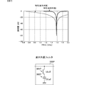
- FIG. 7 is a diagram illustrating attenuation characteristics of the LC parallel resonance circuit and the LC series resonance circuit, and a circuit configuration example of the LC series resonance circuit.
- a filter circuit 300P composed of an LC series resonance circuit includes an inductor 301P and a capacitor 302P. The inductor 301P and the capacitor 302P are connected in series. One end of the series circuit is connected to a predetermined position of a conductor line connecting the phase adjustment circuit 200 and the external connection terminal 141. The other end of the series circuit is connected to the ground.
- the attenuation pole frequency of the notch filter is matched with the frequency of the second harmonic signal. Even with the filter circuit 300P having such a configuration, an operation effect similar to that of the filter circuit 300 including the LC parallel resonance circuit can be obtained.
- the filter circuit 300 of the LC parallel resonance circuit by using the filter circuit 300 of the LC parallel resonance circuit, the attenuation pole characteristics become steeper than when the filter circuit 300P of the LC series resonance circuit is used, as shown in FIG. Therefore, the amount of attenuation other than the second harmonic signal frequency can be reduced. Thereby, a high-frequency signal having a frequency that is not desired to be attenuated, for example, a high-frequency signal having a fundamental frequency, can be transmitted without being attenuated, and the transmission / reception characteristics of the high-frequency switch module 10 can be improved. Since the attenuation band is wide in the LC series resonance circuit, it is easy to attenuate the second harmonic signal even if the second harmonic signal has a width.
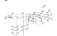
- FIG. 8 is a circuit diagram of a high-frequency switch module according to the second embodiment of the present invention.
- the high-frequency switch module 10A according to the present embodiment omits the filter circuit 300 from the high-frequency switch module 10 according to the first embodiment, and uses a duplexer 700 instead. Except for the circuit configuration related to the duplexer 700, the configuration is the same as that of the high-frequency switch module 10 according to the first embodiment.
- the duplexer 700 includes a first band pass filter 701 and a second band pass filter 702.
- the first band pass filter 701 and the second band pass filter 702 have different pass bands.
- the first band pass filter 701 is connected between the external connection terminal 1411 of the high frequency switch module 10A and the duplexer first terminal.
- the first band pass filter 701 is a filter circuit in which the frequency band of the first high frequency signal input from the external connection terminal 1411 is in the pass band and the frequency band equal to or higher than the frequency of the second harmonic signal is the attenuation band.
- the second band pass filter 702 is connected between the external connection terminal 1412 and the duplexer first terminal of the high frequency switch module 10A.
- the second band pass filter 702 is a filter circuit in which the frequency band of the second high frequency signal output to the external connection terminal 1412 is in the pass band and the frequency band equal to or higher than the frequency of the second harmonic signal is the attenuation band. Further, the second band pass filter 702 is also set so that the frequency of the second harmonic signal of the first high frequency signal is an attenuation band.
- the first high frequency signal and the second high frequency signal are, for example, a transmission signal and a reception signal of the same band class.
- the duplexer 700 is connected to the phase adjustment circuit 200 via the matching circuit 600.
- the matching circuit 600 includes matching circuit inductors 601 and 602.
- the matching circuit inductor 601 is connected between the phase adjustment circuit 200 and the duplexer first terminal of the duplexer 700.
- the matching circuit inductor 602 is connected between the duplexer 700 side of the matching circuit inductor 601 and the ground. Impedance matching between the phase adjustment circuit 200 and the duplexer 700 is performed by appropriately setting element values (inductances) Lt3 and Lu3 of the matching circuit inductors 601 and 602.
- the distorted second harmonic signal output from the individual terminal 111 is reflected by the duplexer 700.
- This utilizes the high reflection coefficient outside the passband of the bandpass filter.
- the distorted second harmonic signal reflected by the duplexer 700 returns to the switch IC 100 and is canceled with the distorted second harmonic signal output from the common terminal 101 at the common terminal 101 as in the first embodiment described above.
- the filter circuit can be omitted.
- the inductances Lt3 and Lu3 of the matching circuit inductors 601 and 602 of the matching circuit 600 in consideration of the action of the phase adjustment circuit 200 to rotate the phase of the second harmonic signal. That is, it is preferable that the phase adjustment amount of the second harmonic signal for cancellation described above is set by the phase adjustment circuit 200 and the matching circuit 600.
- FIG. 9 is a circuit diagram of a high-frequency switch module according to the third embodiment of the present invention.
- the high frequency switch module 10B according to the present embodiment is obtained by adding a filter circuit 300 to the high frequency switch module 10A according to the second embodiment. That is, the high frequency switch module 10 according to the first embodiment and the high frequency switch module 10A according to the second embodiment are combined.
- specific description is abbreviate
- the filter circuit 300 is connected between the phase adjustment circuit 200 and the matching circuit 600. Even if it is such a structure, the effect similar to the above can be acquired. Furthermore, in the present embodiment, the distorted second harmonic signal that passes through the filter circuit 300 and reaches the duplexer 700 is reflected and returned to the switch IC 100. Therefore, the attenuation amount of the amplitude of the distorted second harmonic signal that returns to the common terminal 101 can be further reduced. Thereby, the cancellation effect can be further improved.
- FIG. 10 is a circuit diagram of a high-frequency switch module according to the fourth embodiment of the present invention.
- the high-frequency switch module 10C according to this embodiment is different from the high-frequency switch module 10 according to the first embodiment in the phase adjustment circuit 200C, and other configurations are the high-frequency switch module according to the first embodiment. 10 is the same. Therefore, only different parts will be specifically described.
- the phase adjustment circuit 200C includes a capacitor 201C and inductors 202C and 203C.
- the capacitor 201C is connected between the individual terminal 111 and the filter circuit 300.
- the individual terminal 111 side of the capacitor 201C is connected to the ground via the inductor 202C.
- the filter circuit 300 side of the capacitor 201C is connected to the ground via the inductor 203C.
- the filter circuit 300 is configured similarly to the above-described embodiment.
- the phase of the distorted second harmonic signal that reaches and reflects can be adjusted, and the distorted harmonic signal output from the common terminal 101 can be canceled.
- the phase adjustment circuit 200C is a ⁇ -type high-pass filter (high-pass filter).
- the capacitance Ct1 of the capacitor 201C, the inductance Lu11 of the inductor 202C, and the inductance Lu12 of the inductor 203C are adjusted so that the frequency band of the high-frequency signal is within the pass band and the frequency below this is the attenuation band. Set the filter.
- the signal level of the second harmonic signal reflected by the filter circuit 300 and returned to the switch IC 100 is hardly lowered while transmitting a high-frequency signal having a fundamental frequency with low loss.
- the signal of a frequency lower than the fundamental frequency of a high frequency signal can be interrupted
- the antenna matching circuit 190 uses an inductor and capacitor configuration capable of obtaining an ESD protection effect, thereby realizing ESD protection of the switch IC 100 and further ESD protection of the filter circuit 300.
- FIG. 11 is a circuit diagram of a high-frequency switch module according to the fifth embodiment of the present invention.
- the high-frequency switch module 10D according to the present embodiment is different from the high-frequency switch module 10 according to the first embodiment in the filter circuit 300D, and other configurations are the high-frequency switch module 10 according to the first embodiment. Is the same. Therefore, only different parts will be specifically described.
- the filter circuit 300D is connected between the phase adjustment circuit 200 and the external connection terminal 141, and includes a two-stage LC parallel resonance circuit.
- the filter circuit 300D includes filter inductors 3011 and 3012 and filter capacitors 3021 and 3022.
- the LC parallel circuit of the filter inductor 3011 and the filter capacitor 3021 and the LC parallel circuit of the filter inductor 3012 and the filter capacitor 3022 are connected in this order from the phase adjustment circuit 200 side.
- the frequency of the second harmonic signal is set to the attenuation pole frequency by appropriately setting the inductance Lt21 and the capacitance Ct21 of the LC parallel circuit of the filter inductor 3011 and the filter capacitor 3021. Further, the frequency of the third harmonic signal is set to the attenuation pole frequency by appropriately setting the inductance Lt22 and the capacitance Ct22 of the LC parallel circuit of the filter inductor 3012 and the filter capacitor 3022. These attenuation pole settings may be reversed.
- the attenuation pole frequency of the LC parallel circuit of the filter inductor 3011 and the filter capacitor 3021 is matched with the frequency of the third harmonic signal, and the attenuation pole frequency of the LC parallel circuit of the filter inductor 3012 and the filter capacitor 3022 is 2 You may make it correspond with the frequency of a secondary harmonic signal.
- FIG. 12 is a circuit diagram of a high-frequency switch module according to the sixth embodiment of the present invention.
- the high-frequency switch module 10E of the present embodiment is the same as the high-frequency switch module 10 according to the first embodiment except that the filter circuit 300E is also used as the phase adjustment circuit 200, and other configurations are the same as those of the first embodiment.
- the filter circuit 300E includes a filter inductor 301E and a filter capacitor 302E.
- the filter inductor 301E is connected between the individual terminal 111 and the external connection terminal 141.
- the filter capacitor 302E is connected in parallel to the filter inductor 301E.
- the inductance Lt2E of the filter inductor 301E and the capacitance Ct2E of the filter capacitor 302E are set as appropriate, and the phase rotation function for the second harmonic signal of the phase adjustment circuit 200 described above, and the filter circuit 300 Realize the function.
- the high-frequency switch module can be further reduced in size by omitting the phase adjustment circuit 200 while obtaining the same operational effects as those of the above-described embodiment.
- FIG. 13 is a circuit diagram of a high-frequency switch module according to the seventh embodiment of the present invention.
- the high-frequency switch module 10F of this embodiment is obtained by further adding a second switch IC 100H and a diplexer 800 to the high-frequency switch module 10 according to the first embodiment. Therefore, only different parts will be specifically described.
- the drive control terminals of the switch IC 100 and the second switch IC 100H are omitted.
- the switch IC 100 is for the low band
- the second switch IC 100H is for the high band.
- the low band includes a frequency band of less than 1.5 GHz including the 800 MHz band and the 900 MHz band
- the high band includes a 1.5 GHz band, a 1.8 GHz band, a 1.9 GHz band, etc., and 1.5 GHz or more. Indicates the frequency band.
- the second switch IC 100H includes a common terminal 101H and a plurality of individual terminals 111H, 112H, and 113H.
- the common terminal 101H is connected to any of the individual terminals 111H, 112H, and 113H.
- the duplexer 800 includes a duplexer low-pass filter 801 and a duplexer high-pass filter 802.
- the duplexer low-pass filter 801 is connected between the external connection terminal 130 and the common terminal 101 of the switch IC 100.
- the duplexer high-pass filter 802 is connected between the external connection terminal 130 and the common terminal 101H of the second switch IC 100H.
- the duplexer low-pass filter 801 is set to pass a plurality of low-band high-frequency signals and attenuate a plurality of high-band high-frequency signals.
- the duplexer high-pass filter 802 is set to pass high-frequency signals of a plurality of high-band classes and attenuate high-frequency signals of a plurality of low-band classes.
- the switch IC 100 transmits / receives a low-band band-class high-frequency signal
- the second switch IC 100H transmits / receives a high-band band-class high-frequency signal.
- the frequency of the second harmonic signal generated by the switch IC 100 is close to or partially overlapping with the frequency of the high-band band class, resulting in noise.
- the phase adjustment circuit 200 and the filter circuit 300 are connected to the switch IC 100, the second harmonic signal is hardly output from the common terminal 101 of the switch IC 100. Therefore, the second harmonic signal of the switch IC 100 is not input to the second switch IC 100H. Thereby, the S / N ratio at the time of reception of a high-band band class is improved, and a high-frequency switch module having excellent transmission / reception characteristics can be realized.
- the S / N ratio for receiving a high-band band-class high-frequency signal is high. Can be held. As a result, it is possible to improve the reception characteristics of high-frequency band-class high-frequency signals and to realize a high-frequency switch module with carrier aggregation specifications that is excellent in transmission and reception characteristics.
- FIG. 14 is a circuit diagram of a high-frequency switch module according to the eighth embodiment of the present invention.
- the high-frequency switch module 10G of the present embodiment is obtained by adding a plurality of line conductors 231, 232, 233 and a selection member 230 to the high-frequency switch module 10 according to the first embodiment. This is the same as the high-frequency switch module 10 according to the first embodiment. Therefore, only different parts will be specifically described.
- the plurality of line conductors 231, 232, and 233 have different lengths, and one end is connected to the filter circuit 300.
- the selection member 230 is formed of, for example, a 0 ⁇ resistor or the like, and is arranged so as to connect any one of the other ends of the plurality of line conductors 231, 232, 233 and the phase adjustment circuit 200.
- the line conductor that is not connected by the selection member 230 functions as an open stub. Accordingly, the combination of the selection member 230 and the line conductors 231, 232, and 233 can set the phase adjustment amount of the second harmonic signal in various ways.
- FIG. 15 is a circuit diagram of a high-frequency switch module according to the ninth embodiment of the present invention.
- the high-frequency switch module 10H according to the present embodiment is different from the high-frequency switch module 10G according to the eighth embodiment in that the arrangement positions of the plurality of line conductors 231, 232, 233 and the selection member 230 are different. Is the same as the high-frequency switch module 10G according to the eighth embodiment. Therefore, only different parts will be specifically described.
- One end of the plurality of line conductors 231, 232, 233 is connected to the phase adjustment circuit 200.
- the selection member 230 is disposed so as to connect any one of the other ends of the plurality of line conductors 231, 232, and 233 and the individual terminal 111 of the switch IC 100.
- the line conductor that is not connected by the selection member 230 functions as an open stub. Accordingly, the combination of the selection member 230 and the line conductors 231, 232, and 233 can set the phase adjustment amount of the second harmonic signal in various ways.
- the phase of the distorted second harmonic signal output from the common terminal when the phase of the distorted second harmonic signal output from the individual terminal returns to the common terminal may be 90 ° to 270 °. Thereby, it is possible to suppress at least the distorted second harmonic signal output from the common terminal.
- phase adjustment circuit is realized by a ⁇ -type circuit.
- the phase adjustment circuit can be realized by an L-type circuit or a T-type circuit. Good.
- a phase adjustment function for the second harmonic signal may be provided between the external connection terminals and the individual terminals of the switch IC.
Landscapes
- Engineering & Computer Science (AREA)
- Computer Networks & Wireless Communication (AREA)
- Signal Processing (AREA)
- Power Engineering (AREA)
- Transceivers (AREA)
- Filters And Equalizers (AREA)
Abstract
高周波スイッチモジュール(10)は、スイッチIC(100)、位相調整回路(200)、フィルタ回路(300)を備える。位相調整回路(200)は、インダクタ(201)、キャパシタ(202,203)を備え、個別端子(111)とフィルタ回路(300)との間にインダクタ(201)が直列接続されたπ型回路からなる。フィルタ回路(300)は、フィルタ用インダクタ(301)とフィルタ用キャパシタ(302)のLC並列共振回路である。スイッチIC(100)の個別端子(111)からの歪み2次高調波信号は、位相調整回路(200)を介してフィルタ回路(300で反射され、位相調整回路(200)を介してスイッチIC(100)に戻る。この歪み2次高調波信号は、位相調整回路(200)によって位相調整され、スイッチIC(100)の共通端子(101)に出力される歪み2次高調波信号と相殺される。
Description
本発明は、半導体スイッチを用いて共通端子を複数の個別端子に切り替えて接続することで複数種類の高周波信号を送受信する高周波スイッチモジュールに関する。
複数の高周波信号を共通のアンテナで送受信するための高周波スイッチモジュールが各種考案されている。このような高周波スイッチモジュールでは、一つの共通端子と複数の個別端子とを備えるスイッチICが用いられることがある。スイッチICは、FET(電界効果型トランジスタ)を複数備え、これらFETのON・OFFによって共通端子をいずれか一つの個別端子に接続する。
このような半導体を用いたスイッチICでは、大電力の高周波信号(例えば、送信信号)が入力されると、歪みによる高調波信号が発生する。このような高調波信号が共通端子からアンテナを介して外部に送信されることは、電波干渉等の各種の不具合を生じる原因となる。すなわち、このような歪みによる高調波信号は、高周波スイッチモジュールの帯域外特性を悪化させる原因となる。
したがって、特許文献1に記載の高周波回路では、スイッチICで発生し個別端子に出力された高調波信号を反射するLC直列共振器を備える。LC直列共振器は、スイッチICの個別端子と送信回路とを接続する信号伝送ラインとグランドとの間に接続されている。これにより、個別端子から出力した高調波信号がLC直列共振器の接続点で反射して、スイッチICに戻り、共通端子へ伝送される。この際、信号伝送ラインにおけるLC直列共振器の接続点と個別端子との距離を所定の長さに設定することで、共通端子から出力される高調波信号と、個別端子からLC直列共振器の接続点で反射して共通端子へ出力される高調波信号との位相を逆位相にしている。これにより、アンテナから送信される高調波信号を抑圧している。
しかしながら、特許文献1に記載の従来の高周波回路では、分布定数線路である信号伝送ラインの長さで、個別端子からの高調波信号の位相調整を行っているので、位相を大きく回す場合には、信号伝送ラインを長くしなければならない。この場合、信号伝送ラインを形成する積層体の形状が大きくなってしまう。これにより、高周波回路を小型化することが容易ではない。また、高周波回路の積層モジュールとして限られた形状の中で、最適な位相調整量が得られる信号伝送ラインの長さおよび導体パターンを決定することは容易ではない。したがって、特許文献1に示す従来の構成では、スイッチICを備えた構成であって、高調波歪み特性および帯域外特性に優れた高周波回路を容易且つ小型にすることは困難である。
本発明の目的は、大型化することなく、高調波歪み特性および帯域外特性に優れる高周波スイッチモジュールを提供することにある。
共通端子と複数の個別端子とを有し、半導体スイッチ素子のオンオフによって前記複数の個別端子を前記共通端子に切り替えて接続するスイッチICを備えた高周波スイッチモジュールに関するものである。高周波スイッチモジュールのスイッチICの共通端子および個別端子から高調波信号が出力される。高周波スイッチモジュールは、複数の個別端子の内の第1個別端子と、外部から高周波信号が入力される第1外部接続用端子との間に接続され、高周波信号の高調波成分を減衰させるフィルタ回路を備える。高周波スイッチモジュールは、該フィルタ回路と第1個別端子との間に接続され、インダクタとキャパシタとから構成された位相調整回路を備える。位相調整回路は、共通端子から出力される高調波信号の振幅と、第1個別端子から出力されフィルタ回路で反射して第1個別端子に戻る高調波信号の振幅とが打ち消し合うように、インダクタとキャパシタの素子値が決定されている。
この構成では、第1個別端子から出力された高調波信号は、インダクタとキャパシタを備える位相調整回路を介してフィルタ回路で反射され、位相調整回路、スイッチICを介して共通端子へ出力される。そして、本発明の構成では、位相調整回路がインダクタとキャパシタとを組み合わせて構成されていることで、共通端子に戻される高調波信号の位相調整量を調整しやすい。したがって、従来の分布定数線路による位相調整回路と比較して、所望の位相調整量を得るための形状自由度が向上し、小型化し易く、高調波歪み特性および帯域外特性を向上しやすい。
また、この発明の高周波スイッチモジュールでは、インダクタとキャパシタは、共通端子からの高調波信号と第1個別端子からの高調波信号の位相差が90°から270°の間となるように、素子値が決定されていることが好ましい。
この構成では、共通端子からの高調波信号と第1個別端子からの高調波信号とが少なくとも互いに打ち消し合い、共通端子から出力される高調波信号のレベルを抑圧できる。
また、この発明の高周波スイッチモジュールでは、インダクタとキャパシタは、共通端子からの高調波信号と第1個別端子からの高調波信号の位相差が180°となるように素子値が決定されていることが好ましい。
この構成では、共通端子からの高調波信号と第1個別端子からの高調波信号とが完全に相殺され、共通端子から高調波信号が出力されない。
また、この発明の高周波スイッチモジュールの位相調整回路は、高調波信号の周波数帯域を通過帯域内とする低域通過フィルタであることが好ましい。
この構成では、位相調整回路で、相殺用の高調波信号の位相調整とともに、フィルタ回路側から入力される高周波信号を基本波とするさらに高次の高調波信号(例えば、上述の高調波信号が2次高調波信号であれば3次以上の高調波信号)を減衰できる。
また、この発明の高周波スイッチモジュールの位相調整回路は、高周波信号の周波数帯域を通過帯域内とする高域通過フィルタであってもよい。
この構成では、位相調整回路で、相殺用の高調波信号の位相調整とともに、スイッチICの共通端子側から入力される静電気を抑圧できる。これにより、フィルタ回路のESD効果が高まり、高周波スイッチモジュールのESD効果が向上する。
また、この発明の高周波スイッチモジュールのフィルタ回路は、高調波信号の周波数が減衰極周波数に略一致するノッチフィルタである。
この構成では、入力される大電力の高周波信号の高調波信号を効果的に減衰させることができるとともに、スイッチICで発生した高調波信号がフィルタ回路から位相調整回路側へ反射する反射量を大きいまま維持できる。これにより、共通端子から出力される高調波信号のレベルとフィルタ回路から反射される高調波信号のレベルとのレベル差が小さくなり、相殺効果が向上する。
また、この発明の高周波スイッチモジュールでは、次の構成であることが好ましい。フィルタ回路は、フィルタ用キャパシタとフィルタ用インダクタとが並列接続されたLC並列共振回路を備える。該LC並列共振回路は、第1外部接続用端子と位相調整回路との間に接続されている。
この構成では、高調波信号の周波数帯域以外での通過特性がよく、高周波スイッチモジュールとしての送受信特性を向上させることができる。
また、この発明の高周波スイッチモジュールでは、次の構成であってもよい。フィルタ回路は、フィルタ用キャパシタとフィルタ用インダクタとが直列接続されたLC直列共振回路を備える。LC直列共振回路は、第1外部接続用端子と位相調整回路との接続ラインと、グランドとの間に接続されている。
この構成では、上述のLC並列共振回路を用いた場合のような作用効果は得られないが、所定の減衰量以上の減衰量を得られる周波数帯域が広く、高調波信号の周波数がずれても、高調波信号の反射量が低減しにくい。
また、この発明の高周波スイッチモジュールでは、フィルタ回路は、高周波信号の周波数帯域を通過帯域内とする帯域通過フィルタであってもよい。
この構成では、高調波信号の周波数が帯域通過フィルタの減衰帯域内となる。帯域通過フィルタは、通過帯域外の減衰量すなわち反射量が大きいので、フィルタ回路で反射される高調波信号のレベルが低下しにくい。
また、この発明の高周波スイッチモジュールでは、帯域通過フィルタは、デュプレクサを構成する一つのフィルタであってもよい。
この構成では、第1外部接続用端子にデュプレクサが接続されるような態様の場合に、デュプレクサと別にフィルタ回路を設ける必要が無く、高周波スイッチモジュールを小さく構成することができる。
また、この発明の高周波スイッチモジュールは、次の構成であることが好ましい。高周波スイッチモジュールの上述のスイッチICはローバンド用のスイッチICである。さらに、高周波スイッチモジュールは、ハイバンド用の第2のスイッチICと、アンテナへの接続端子、スイッチICの共通端子に接続するローバンド側端子、および第2のスイッチICの共通端子に接続するハイバンド側端子を備え、ローバンドの高周波信号とハイバンドの高周波信号とを分波するアンテナ側分波器と、を備える。第1個別端子に入力される高周波信号と、第2のスイッチ回路を伝送する第2高周波信号とが、少なくとも一時的に同時通信される。
この構成では、キャリアアグリゲーション等の複数のバンドクラス(周波数領域)で同時に高周波信号を送受信する高周波スイッチモジュールにおいて、ローバンドの高周波信号の高調波信号が、ハイバンド側の回路に回り込むことを抑制できる。
また、この発明の高周波スイッチモジュールは、次の構成であってもよい。フィルタ回路と位相調整回路との間に、複数の線路導体と選択部材とが備えられている。複数の線路導体は、フィルタ回路に接続し、異なる長さからなる。選択部材は、複数の線路導体を位相調整回路に選択して接続する。
また、この発明の高周波スイッチモジュールは、次の構成であってもよい。位相調整回路と第1個別端子の間に、複数の線路導体と選択部材とが備えられている。複数の線路導体は、位相調整回路に接続し、異なる長さからなる。選択部材は、複数の線路導体を第1個別端子に選択して接続する。
これらの構成では、接続された線路導体以外はオープンスタブとなるので、これらオープンスタブにより、高調波信号に対する更なる位相調整が可能になる。そして、選択する線路導体によってオープンスタブの形状が異なるので、異なる位相調整量を選択でき、適する位相調整量を適宜選択しやすい。
また、この発明の高周波スイッチモジュールは、次の構成であることが好ましい。高周波スイッチモジュールは、導体パターンが形成された誘電体層を複数積層してなる積層体によって形成されている。位相調整回路のインダクタは、積層体に実装される実装型インダクタ素子である。位相調整回路のキャパシタは、積層体に実装される実装型キャパシタ素子である。
この構成では、位相調整量に依存することなく、位相調整回路の形状を小さくできる。また、各実装型素子を置き換えるだけで、位相調整量を変化させることができる。これにより、適する位相調整量を容易に実現でき、且つ小型化が可能である。
また、この発明の高周波スイッチモジュールでは、次の構成であることが好ましい。フィルタ回路のインダクタは、積層体に実装される実装型インダクタ素子である。フィルタ回路のキャパシタは、積層体に実装される実装型キャパシタ素子である。
この構成では、さらに、適する位相調整量を容易に実現でき、且つ小型化が可能な高周波スイッチモジュールを実現できる。
この発明によれば、高調波歪み特性および帯域外特性に優れる高周波スイッチモジュールを小型且つ容易に実現することができる。
本発明の第1の実施形態に係る高周波スイッチモジュールについて、図を参照して説明する。図1は、本発明の第1の実施形態に係る高周波スイッチモジュールの回路図である。なお、本実施形態では、1個の共通端子と3個の個別端子を有するスイッチICを例に説明するが、個別端子数はこれに限るものではなく、複数であれば他の個数であってもよい。
高周波スイッチモジュール10は、スイッチIC100、位相調整回路200、フィルタ300、アンテナ整合回路190を備える。高周波スイッチモジュール10は、外部接続用端子130,141,142,143,151,152,153を備える。外部接続用端子141が、本発明の「第1外部接続用端子」に相当する。外部接続用端子130は、高周波スイッチモジュール10の外部に配置されたアンテナANTに接続されている。
スイッチIC100は、共通端子101、個別端子111,112,113、駆動制御端子121,122,123を備える。個別端子111が本発明の「第1個別端子」に相当する。スイッチIC100は、駆動制御端子121,122,123に入力される駆動電圧と制御信号によって、共通端子101を、個別端子111,112,113のいずれか1個に切り替えて接続する。より具体的には、スイッチIC100は、FET(電界効果型トランジスタ)等の半導体スイッチが共通端子101と各個別端子111,112,113との間に接続される構造からなる。スイッチIC100は、駆動電圧で半導体スイッチに電源供給し、制御信号によって、オン制御する半導体スイッチとオフ制御する半導体スイッチを切り替える。スイッチIC100は、このような各半導体スイッチのオンオフ制御によって、共通端子101を個別端子111,112,113のいずれかに接続する。
共通端子101と外部接続用端子130との間には、アンテナ整合回路190が接続されている。アンテナ整合回路190は、図示していないが、例えば、直列インダクタ、該直列インダクタと外部接続用端子130との間をグランドに接続するキャパシタ、直列インダクタと共通端子101との間をグランドに接続するインダクタ等のから構成される。
駆動制御端子121,122,123は、それぞれ外部接続用端子151,152,153に接続する。これら外部接続用端子151,152,153から駆動電圧および制御信号が供給される。
個別端子111は、位相調整回路200、フィルタ回路300を介して、外部接続用端子141に接続されている。
個別端子112,113は、それぞれ外部接続用端子142,143に接続されている。なお、これらの個別端子と外部接続用端子との間に、フィルタ等の回路素子が接続されていてもよい。
位相調整回路200は、個別端子111とフィルタ回路300との間に接続されている。位相調整回路200は、インダクタ201、キャパシタ202,203を備える。インダクタ201は、個別端子111とフィルタ回路300との間に直列接続されている。インダクタ201の個別端子111側は、キャパシタ202を介してグランドに接続されている。インダクタ201のフィルタ回路300側は、キャパシタ203を介してグランドに接続されている。
インダクタ201のインダクタンスLt1、キャパシタ202のキャパシタンスCu1、キャパシタ203のキャパシタンスCu2は、後述する2次高調波信号の位相シフト条件に基づいて設定されている。
フィルタ回路300は、フィルタ用インダクタ301、フィルタ用キャパシタ302を備える。フィルタ用インダクタ301は、位相調整回路200と外部接続用端子141との間に接続されている。フィルタ用キャパシタ302は、フィルタ用インダクタ301に並列接続されている。これにより、フィルタ回路300は、フィルタ用インダクタ301とフィルタ用キャパシタ302とのLC並列共振回路からなる。このような回路構成から、フィルタ回路300は、LC並列共振型のノッチフィルタとして機能する。
フィルタ用インダクタ301の素子値(インダクタンス)Lt2とフィルタ用キャパシタ302の素子値(キャパシタンス)Ct2は、外部接続用端子141から入力される高周波信号の2次高調波信号の周波数がノッチフィルタの減衰極周波数と一致もしくは略一致するように設定されている。
図2は、外部接続用端子から高周波信号(大電力)が入力された場合の当該高周波信号の伝送状態を説明する図である。なお、本発明でいう「大電力」とは、高周波スイッチモジュール10に用いられるスイッチIC100に高周波信号が入力されたことにより、当該スイッチIC100から歪み高調波信号が発生する電力レベルを示す。図3は、高周波信号の2次高調波信号の伝送状態、および歪み2次高調波信号の伝送状態を示す図である。なお、図2、図3では、スイッチIC100の個別端子111と共通端子101が導通された状態を示す。
図2に示すように、外部接続用端子141から入力された基本周波数の高周波信号(基本波)Sf0は、フィルタ回路300、位相調整回路200を介して、スイッチIC100の個別端子111に入力される。スイッチIC100の個別端子111に入力された高周波信号Sf0は、共通端子101から出力される。
図3(上段)に示すように、外部接続用端子141から入力された高周波信号の2次高調波信号S2f0は、フィルタ回路300で減衰される。これにより、入力された2次高調波信号S2f0は、位相調整回路200およびスイッチIC100には伝送されず、スイッチIC100の共通端子101から出力されない。
基本周波数の高周波信号Sf0がスイッチIC100に入力されると、高周波信号Sf0が大電力の場合に、半導体スイッチが歪んで、歪み高調波信号が発生する。なお、歪み高調波信号の電力は、殆どが2次高調波信号SD2f0である。この歪み2次高調波信号SD2f0は、共通端子101、個別端子111に出力される。
個別端子111に出力された歪み2次高調波信号SD2f0は、位相調整回路200を介して、フィルタ回路300に伝送される。フィルタ回路300は、2次高調波信号の周波数が減衰極周波数と一致するので、歪み2次高調波信号SD2f0は、フィルタ回路300で反射する。この反射2次高調波信号SDR2f0は、位相調整回路200を伝送し、個別端子111に入力される。反射2次高調波信号SDR2f0は、個別端子111から共通端子101に伝送される。
したがって、共通端子101からは、元々共通端子101から出力される歪み2次高調波信号SDc2f0と反射2次高調波信号SDR2f0とが重なり合って出力される。
ここで、共通端子101での歪み2次高調波信号SDc2f0の位相と反射2次高調波信号SDR2f0の位相とが逆位相となるように、位相調整回路200のインダクタ201のインダクタンスLt1、キャパシタ202のキャパシタンスCu1、キャパシタ203のキャパシタンスCu2を決定する。言い換えれば、個別端子111から出力された歪み2次高調波信号がフィルタ回路300で反射してスイッチIC100に戻り、共通端子101における反射2次高調波信号SDR2f0の位相が、共通端子101での歪み2次高調波信号SDc2f0の位相に対して180°シフトしているように、位相調整回路200のインダクタ201のインダクタンスLt1、キャパシタ202のキャパシタンスCu1、キャパシタ203のキャパシタンスCu2を決定する。
このような構成とすることで、図3(下段)に示すように、共通端子101において歪み2次高調波信号SDc2f0と反射2次高調波信号SDR2f0とが相殺され、結果的に、共通端子101から2次高調波信号が出力されていない状態となる。これにより、2次高調波信号が外部接続用端子130(アンテナANT)側に出力されず、高周波スイッチモジュール10の高調波歪み特性および帯域外特性が改善する。高調波歪み特性とは、送受信する高周波信号の周波数を基本波周波数とする高調波信号が外部へ出力されにくいほど良好となる特性である。帯域外特性とは、送受信する周波数帯域以外の周波数帯域で大きな減衰量が得られる場合が良好となる特性である。
さらに、本実施形態に示すように、位相調整回路200が、インダクタ201とキャパシタ202,203によって構成されているので、分布定数線路であるマイクロストリップラインの構成よりも、共通端子101に戻る2次高調波信号の位相を調整しやすい。したがって、従来の分布定数線路による位相調整回路と比較して、所望の位相調整量を得るための形状自由度が向上し、小型化がより容易に実現できる。
図4は、本実施形態の構成および従来構成でのアンテナANTでの2次高調波レベルをシミュレーションした結果である。なお、図4では、従来構成でスイッチICのFETの形状を2倍にした構成についても示している。また、図4のシミュレーションは、入力される高周波信号のレベルを+26[dBm]としている。
図4に示すように、従来構成では-80[dBm]であった2次高調波レベルが、本実施形態の構成では-95[dBm]まで低下する。一般に、スイッチICのFETの形状を大きくすることで、高調波信号の出力を抑制できることが知られている。そこで、従来の構成のスイッチICの形状を2倍にした場合の構成についても、シミュレーションしている。その結果、従来構成でスイッチICのFETの形状を2倍にした構成では-83[dBm]であるので、この構成よりも、本実施形態の構成の方が2次高調波レベルを低下することができる。
また、上述の構成では、位相調整回路200は、π型の低域通過フィルタ(ローパスフィルタ)となる。ここで、インダクタ201のインダクタンスLt1、キャパシタ202のキャパシタンスCu1、キャパシタ203のキャパシタンスCu2を調整し、2次高調波信号の周波数を通過周波数帯域内とし、3次高調波信号の周波数帯域が減衰帯域となるように、低域通過フィルタを設定する。
このような構成とすることで、フィルタ回路300で反射してスイッチIC100に戻る2次高調波信号の信号レベルを殆ど低下させない。したがって、共通端子101での相殺効果を向上させることができる。これにより、共通端子101から出力される2次高調波信号を、より大幅に抑圧することができ、高周波スイッチモジュール10の高調波歪み特性および帯域外特性を、さらに向上させることができる。
さらに、フィルタ回路300を通過した3次以上の高調波信号が、位相調整回路200で減衰されるので、共通端子101から出力される2次以上の高調波信号も大幅に抑圧することができる。これにより、高周波スイッチモジュール10の総合的に高調波歪み特性および帯域外特性を、さらに向上させることができる。
上述のような高周波スイッチモジュール10は、複数の誘電体層を積層した積層体によって実現される。所定の誘電体層には、高周波スイッチモジュール10の回路パターンを実現するための導体パターンが形成されている。積層体の天面には、実装型回路素子が実装されており、積層体の底面には、外部接続用端子を実現する実装用ランドが形成されている。
図5は、本実施形態の一態様となる高周波スイッチモジュールの積層図である。なお、図5の各誘電体層に記載された○(丸形状)は誘電体層を厚み方向に貫通する導電性ビアを示す。図6は、図5の積層図のパターンにより実現される高周波モジュールの回路図である。
図5、図6に示す高周波スイッチモジュール10Rは、スイッチIC100R、アンテナ整合回路190、位相調整回路200、フィルタ回路300、低域通過フィルタ400,500を備える。位相調整回路200およびフィルタ回路300は、上述の高周波スイッチモジュール10と同じである。
高周波スイッチモジュール10Rは、外部接続用端子130,141-149,151-155を備える。
スイッチIC100Rは、1個の共通端子101、9個の個別端子111-119、5個の駆動制御端子121-125を備える。駆動制御端子121-125に供給される駆動電圧と制御信号とにより、共通端子101は、個別端子111-119のいずれかに接続される。
共通端子101と外部接続用端子130との間には、アンテナ整合用インダクタ191が接続されている。アンテナ整合回路190は、アンテナ整合用インダクタ191,192、およびアンテナ整合用キャパシタ193を備える。アンテナ整合用インダクタ191は、共通端子101と外部接続用端子130との間に接続されている。アンテナ整合用インダクタ191の共通端子101側は、アンテナ整合用インダクタ192を介してグランドに接続されている。アンテナ整合用インダクタ191の外部接続用端子130側は、アンテナ整合用キャパシタ193を介してグランドに接続されている。
個別端子111と外部接続用端子141との間には、位相調整回路200とフィルタ回路300が接続されている。
個別端子112と外部接続用端子142との間には、低域通過フィルタ400が接続されている。低域通過フィルタ400は、LPF用インダクタ401,402、LPF用キャパシタ411,412,421,422,423を備える。LPF用インダクタ401,402は、個別端子112と外部接続用端子142との間に直列接続されている。LPF用キャパシタ411は、LPF用インダクタ401に並列接続されている。LPF用キャパシタ412は、LPF用インダクタ402に並列接続されている。LPF用インダクタ401の個別端子112側は、LPF用キャパシタ421を介してグランドに接続されている。LPF用インダクタ401,402の接続点は、LPF用キャパシタ422を介してグランドに接続されている。LPF用インダクタ402の外部接続用端子142側は、LPF用キャパシタ423を介してグランドに接続されている。低域通過フィルタ400は、外部接続用端子142に入力される高周波信号の周波数帯域が通過帯域内となり、2次高調波周波数以上が減衰帯域となるように、各LPF用インダクタ401,402及びLPF用キャパシタ411,412,421,422,423の素子値が決定されている。
個別端子113と外部接続用端子143との間には、低域通過フィルタ500が接続されている。低域通過フィルタ500は、LPF用インダクタ501,502、LPF用キャパシタ511,522を備える。LPF用キャパシタ511は、LPF用インダクタ501に並列接続されている。LPF用インダクタ501,502の接続点は、LPF用キャパシタ522を介してグランドに接続されている。低域通過フィルタ500は、外部接続用端子143に入力される高周波信号の周波数帯域が通過帯域内となり、2次高調波周波数以上が減衰帯域となるように、各LPF用インダクタ501,502及びLPF用キャパシタ511,522の素子値が決定されている。
個別端子114-119は、それぞれ外部接続用端子144-149に接続されている。駆動制御端子121-125は、それぞれ外部接続用端子151-155に接続されている。
このような高周波スイッチモジュール10Rは、図5に示すように、誘電体層Lay1から誘電体層Lay14の14層を積層してなる積層体によって実現される。誘電体層Lay1が積層体の最上層であり、誘電体層Lay14が積層体の最下層である。誘電体層Lay1から誘電体層Lay13では導体パターンが上層側に形成されており、誘電体層Lay14では導体パターンが下層側に形成されている。
最上層(第1層)となる誘電体層Lay1の天面(積層体の天面)には、スイッチIC100、インダクタ201、キャパシタ202,203、フィルタ用インダクタ301、フィルタ用キャパシタ302、アンテナ整合用インダクタ191,192、アンテナ整合用キャパシタ193が実装されている。これらの回路素子は、実装型回路素子からなり、天面に形成された素子用ランドに実装されている。インダクタ201、キャパシタ202,203、フィルタ用インダクタ301、フィルタ用キャパシタ302は、スイッチIC100を挟んで、アンテナ整合用インダクタ191,192、アンテナ整合用キャパシタ193から離間されている。
位相調整回路200を構成するインダクタ201、キャパシタ202,203は、互いに並ぶように近接して実装されている。さらに、フィルタ用インダクタ301、フィルタ用キャパシタ302も互いに並ぶように近接して実装されており、且つインダクタ201、キャパシタ202,203と並ぶように近接して実装されている。このような構成により、位相調整回路200の各回路素子を接続する導体パターンを短くでき、この導体パターンによる位相シフト量を極小さくできる。また、位相調整回路200とフィルタ回路300とを接続する導体パターンも短くでき、この導体パターンによる位相シフト量を極小さくできる。これにより、スイッチIC100に戻る2次高調波信号の位相シフト量を、インダクタ201、キャパシタ202,203で正確に設定することができる。
第2層である誘電体層Lay2および第3層である誘電体層Lay3には、引き回し用導体パターンが適宜形成されている。スイッチIC100、インダクタ201、キャパシタ202,203、フィルタ用インダクタ301、フィルタ用キャパシタ302を接続する導体パターンは、これらの誘電体層に形成されている。これにより、さらに高精度に、スイッチIC100に戻る2次高調波信号の位相シフト量を、インダクタ201、キャパシタ202,203で設定することができる。
第4層である誘電体層Lay4には、略全面に内装グランド導体PtGND1が形成されている。
第5層である誘電体層Lay5には、引き回し用導体パターンが適宜形成されている。
第6層である誘電体層Lay6には、内装グランド導体PtGND2と、キャパシタ421用の矩形導体が形成されている。内装グランド導体PtGND2は、内装グランド導体PtGND1とともに誘電体層Lay5の引き回し用導体パターンを積層方向に沿って挟むように形成されている。
第7層、第8層、第9層である誘電体層Lay7,Lay8,Lay9には、低域通過フィルタ用インダクタ401,402,501,502用の線状巻回導体が形成されている。
第10層である誘電体層Lay10には、低域通過フィルタ用キャパシタ511用の矩形導体が形成されている。第11層である誘電体層Lay11には、低域通過フィルタ用キャパシタ411,412用の矩形導体が形成されている。第12層である誘電体層Lay12には、低域通過フィルタ用キャパシタ411,412,422,423,511,522用の矩形導体が形成されている。
第13層である誘電体層Lay13には、略全面に内装グランド導体PtGND3が形成されている。
第14層(最下層)である誘電体層Lay14には、外部接続用端子130,141,142-149,151-155用の外部接続用ランドと、外部グランド接続用ランドPGが形成されている。
このように、位相調整回路200を構成するインダクタ201、キャパシタ202,203を実装回路素子とすることで、位相シフト量を大きくとっても、積層体の形状を小型にすることができる。さらに、フィルタ回路300を構成するフィルタ用インダクタ301およびフィルタ用キャパシタ302を実装回路素子とすることでも、積層体の形状を小型にすることができる。
また、このような構成とすることで、位相調整回路200およびフィルタ回路300と、低域通過フィルタ400,500との間に内装グランド導体PtGND1が配置される。これにより、位相調整回路200およびフィルタ回路300と、低域通過フィルタ400,500とが積層方向に見て重なっていても、位相調整回路200およびフィルタ回路300と低域通過フィルタ400,500との間のアイソレーションを高く確保することができる。すなわち、これらのアイソレーションを高く確保しつつ、高周波スイッチモジュール10を小型に形成することができる。
また、アンテナANTに接続する外部接続用端子130用の外部接続用ランドは、他の外部接続用ランドに対して、グランド接続用ランドPGを挟んで離間されている。これにより、アンテナANTに接続する外部接続用端子130用の外部接続用ランドと、他の外部接続用ランドとの間のアイソレーションを高く確保することができる。
なお、上述の高周波スイッチモジュールでは、フィルタ回路300としてLC並列共振回路のノッチフィルタを用いた。しかしながら、LC直列共振回路のノッチフィルタに置き換えることも可能である。図7は、LC並列共振回路およびLC直列共振回路の減衰特性と、LC直列共振回路の回路構成例を示す図である。LC直列共振回路からなるフィルタ回路300Pは、インダクタ301Pとキャパシタ302Pを備える。インダクタ301Pとキャパシタ302Pは直列接続されている。この直列回路の一方端は、位相調整回路200と外部接続用端子141とを接続する導体ラインの所定位置に接続されている。直列回路の他方端は、グランドに接続されている。インダクタ301Pの素子値(インダクタンス)LLu2とキャパシタ302Pの素子値(キャパシタンス)CCu2を適宜設定することで、ノッチフィルタの減衰極周波数を2次高調波信号の周波数に一致させる。このような構成のフィルタ回路300Pでも、LC並列共振回路からなるフィルタ回路300と類似する作用効果が得られる。
しかしながら、LC並列共振回路のフィルタ回路300を用いることで、図7に示すように、LC直列共振回路のフィルタ回路300Pを用いるよりも、減衰極特性が急峻になる。したがって、2次高調波信号周波数以外の減衰量を小さくできる。これにより、減衰させたくない周波数の高周波信号、例えば基本周波数の高周波信号を減衰させずに伝送することができ、高周波スイッチモジュール10としての送受信特性を向上させることができる。なお、LC直列共振回路では減衰帯域が広くなるので、2次高調波信号に幅があっても、2次高調波信号を減衰させやすくなる。
次に、第2の実施形態に係る高周波スイッチモジュールについて、図を参照して説明する。図8は本発明の第2の実施形態に係る高周波スイッチモジュールの回路図である。本実施形態の高周波スイッチモジュール10Aは、第1の実施形態に係る高周波スイッチモジュール10に対して、フィルタ回路300を省略し、代わりにデュプレクサ700を用いている。当該デュプレクサ700に関わる回路構成以外は、第1の実施形態に係る高周波スイッチモジュール10と同じであるので、具体的な説明は省略する。
デュプレクサ700は、第1帯域通過フィルタ701、第2帯域通過フィルタ702を備える。第1帯域通過フィルタ701と第2帯域通過フィルタ702は、通過帯域が異なる。第1帯域通過フィルタ701は、高周波スイッチモジュール10Aの外部接続用端子1411とデュプレクサ第1端子との間に接続されている。第1帯域通過フィルタ701は、外部接続用端子1411から入力される第1高周波信号の周波数帯域を通過帯域内とし、2次高調波信号の周波数以上の周波数帯域を減衰帯域とするフィルタ回路である。第2帯域通過フィルタ702は、高周波スイッチモジュール10Aの外部接続用端子1412とデュプレクサ第1端子との間に接続されている。第2帯域通過フィルタ702は、外部接続用端子1412へ出力する第2高周波信号の周波数帯域を通過帯域内とし、2次高調波信号の周波数以上の周波数帯域を減衰帯域とするフィルタ回路である。さらに、第2帯域通過フィルタ702は、第1高周波信号の2次高調波信号の周波数を減衰帯域とするようにも設定されている。第1高周波信号と第2高周波信号は、例えば、同じバンドクラスの送信信号と受信信号である。
デュプレクサ700は、整合回路600を介して、位相調整回路200に接続されている。整合回路600は、整合回路用インダクタ601,602を備える。整合回路用インダクタ601は、位相調整回路200とデュプレクサ700のデュプレクサ第1端子との間に接続されている。整合回路用インダクタ602は、整合回路用インダクタ601のデュプレクサ700側とグランドとの間に接続されている。整合回路用インダクタ601,602の素子値(インダクタンス)Lt3,Lu3を適宜設定することで、位相調整回路200とデュプレクサ700との間のインピーダンス整合を行っている。
このような構成では、個別端子111から出力される歪み2次高調波信号は、デュプレクサ700で反射される。これは、帯域通過フィルタの通過帯域外での反射係数が高いことを利用している。デュプレクサ700で反射した歪み2次高調波信号は、スイッチIC100に戻り、上述の第1の実施形態と同様に、共通端子101で当該共通端子101から出力される歪み2次高調波信号と相殺される。
以上のように、個別端子111にデュプレクサが接続される態様では、フィルタ回路を省略することができる。
なお、位相調整回路200が2次高調波信号の位相を回転させる作用を加味して、整合回路600の整合回路用インダクタ601,602のインダクタンスLt3,Lu3を設定することが好ましい。すなわち、位相調整回路200と整合回路600とで、上述の相殺用の2次高調波信号の位相回転量を設定するようにすることが好ましい。
次に、第3の実施形態に係る高周波スイッチモジュールについて、図を参照して説明する。図9は本発明の第3の実施形態に係る高周波スイッチモジュールの回路図である。本実施形態の高周波スイッチモジュール10Bは、第2の実施形態に係る高周波スイッチモジュール10Aに対して、フィルタ回路300を追加したものである。すなわち、第1の実施形態に係る高周波スイッチモジュール10と、第2の実施形態に係る高周波スイッチモジュール10Aとを組み合わせたものである。なお、第2の実施形態に係る高周波スイッチモジュール10Aと同じ箇所については、具体的な説明は省略する。
フィルタ回路300は、位相調整回路200と整合回路600との間に接続されている。このような構成であっても、上述と同様の作用効果を得ることができる。さらに、本実施形態では、フィルタ回路300を通過して、デュプレクサ700に達した歪み2次高調波信号が反射して、スイッチIC100に戻る。したがって、共通端子101に戻る歪み2次高調波信号の振幅の減衰量を、より少なくすることができる。これにより、さらに相殺効果を向上させることができる。
次に、第4の実施形態に係る高周波スイッチモジュールについて、図を参照して説明する。図10は本発明の第4の実施形態に係る高周波スイッチモジュールの回路図である。本実施形態の高周波スイッチモジュール10Cは、第1の実施形態に係る高周波スイッチモジュール10に対して、位相調整回路200Cが異なるものであり、他の構成は、第1の実施形態に係る高周波スイッチモジュール10と同じである。したがって、異なる箇所のみを具体的に説明する。
位相調整回路200Cは、キャパシタ201C、インダクタ202C,203Cを備える。キャパシタ201Cは、個別端子111とフィルタ回路300との間に接続されている。キャパシタ201Cの個別端子111側は、インダクタ202Cを介してグランドに接続されている。キャパシタ201Cのフィルタ回路300側は、インダクタ203Cを介してグランドに接続されている。そして、キャパシタ201Cの素子値(キャパシタンス)Ct1、インダクタ202Cの素子値(インダクタンス)Lu11、インダクタ203Cの素子値(インダクタンス)Lu12を適宜設定することで、上述の実施形態と同様に、フィルタ回路300に達して反射する歪み2次高調波信号の位相を調整し、共通端子101から出力される歪み高調波信号を相殺することができる。
また、位相調整回路200Cは、π型の高域通過フィルタ(ハイパスフィルタ)となる。ここで、キャパシタ201CのキャパシタンスCt1、インダクタ202CのインダクタンスLu11、インダクタ203CのインダクタンスLu12を調整し、高周波信号の周波数帯域が通過帯域内となり、これ以下の周波数が減衰帯域となるように、高域通過フィルタを設定する。
このような構成とすることで、基本周波数の高周波信号を低損失で伝送しながら、フィルタ回路300で反射してスイッチIC100に戻る2次高調波信号の信号レベルを殆ど低下させない。そして、高周波信号の基本周波数よりも低い周波数の信号を遮断できる。これにより、アンテナANTから入力されたサージを遮断し、フィルタ回路300に伝送されないようにすることができ、フィルタ回路300および外部接続端子141に接続される他の素子のESD保護を実現できる。なお、この際、アンテナ整合回路190で、ESD保護効果を得られるインダクタとキャパシタの構成を用いることで、スイッチIC100のESD保護と、フィルタ回路300のさらなるESD保護を実現できる。
次に、第5の実施形態に係る高周波スイッチモジュールについて、図を参照して説明する。図11は本発明の第5の実施形態に係る高周波スイッチモジュールの回路図である。本実施形態の高周波スイッチモジュール10Dは、第1の実施形態に係る高周波スイッチモジュール10に対して、フィルタ回路300Dが異なるものであり、他の構成は、第1の実施形態に係る高周波スイッチモジュール10と同じである。したがって、異なる箇所のみを具体的に説明する。
フィルタ回路300Dは、位相調整回路200と外部接続用端子141との間に接続されており、2段のLC並列共振回路からなる。フィルタ回路300Dは、フィルタ用インダクタ3011,3012、フィルタ用キャパシタ3021,3022を備える。フィルタ用インダクタ3011とフィルタ用キャパシタ3021のLC並列回路と、フィルタ用インダクタ3012とフィルタ用キャパシタ3022のLC並列回路とが、この順で位相調整回路200側から接続されている。
そして、フィルタ用インダクタ3011とフィルタ用キャパシタ3021のLC並列回路のインダクタンスLt21およびキャパシタンスCt21を適宜設定することで、2次高調波信号の周波数を減衰極周波数に設定している。また、フィルタ用インダクタ3012とフィルタ用キャパシタ3022のLC並列回路のインダクタンスLt22およびキャパシタンスCt22を適宜設定することで、3次高調波信号の周波数を減衰極周波数に設定している。なお、これら減衰極の設定は逆であってもよい。すなわち、フィルタ用インダクタ3011とフィルタ用キャパシタ3021のLC並列回路の減衰極周波数を3次高調波信号の周波数に一致させ、フィルタ用インダクタ3012とフィルタ用キャパシタ3022のLC並列回路の減衰極周波数を2次高調波信号の周波数に一致させてもよい。
このような構成であっても、上述の実施形態と同様の作用効果を得ることができる。さらに、3次以上の高調波信号も遮断でき、高周波スイッチモジュール10Dの高調波歪み特性および帯域外特性を向上させることができる。
次に、第6の実施形態に係る高周波スイッチモジュールについて、図を参照して説明する。図12は本発明の第6の実施形態に係る高周波スイッチモジュールの回路図である。本実施形態の高周波スイッチモジュール10Eは、第1の実施形態に係る高周波スイッチモジュール10に対して、フィルタ回路300Eで位相調整回路200を兼用したものであり、他の構成は、第1の実施形態に係る高周波スイッチモジュール10と同じである。したがって、異なる箇所のみを具体的に説明する。
フィルタ回路300Eは、フィルタ用インダクタ301Eとフィルタ用キャパシタ302Eを備える。フィルタ用インダクタ301Eは、個別端子111と外部接続用端子141との間に接続されている。フィルタ用キャパシタ302Eは、フィルタ用インダクタ301Eに並列接続されている。
このような構成において、フィルタ用インダクタ301EのインダクタンスLt2Eと、フィルタ用キャパシタ302EのキャパシタンスCt2Eを、適宜設定して、上述の位相調整回路200の2次高調波信号に対する位相回転機能と、フィルタ回路300の機能を実現する。このような構成とすることで、上述の実施形態と同様の作用効果を得ながら、位相調整回路200を省略して、高周波スイッチモジュールをさらに小型に形成することができる。
次に、第7の実施形態に係る高周波スイッチモジュールについて、図を参照して説明する。図13は本発明の第7の実施形態に係る高周波スイッチモジュールの回路図である。本実施形態の高周波スイッチモジュール10Fは、第1の実施形態に係る高周波スイッチモジュール10に対して、さらに、第2のスイッチIC100H、ディプレクサ800、を追加したものである。したがって、異なる箇所のみを具体的に説明する。なお、図13では、スイッチIC100および第2のスイッチIC100Hの駆動制御端子は省略している。スイッチIC100がローバンド用であり、第2のスイッチIC100Hがハイバンド用である。なお、例えば、ローバンドとは800MHz帯や900MHz帯を含み1.5GHz未満の周波数帯域を示し、ハイバンドとは1.5GHz帯や1.8GHz帯、1.9GHz帯等を含み、1.5GHz以上の周波数帯域を示す。
第2のスイッチIC100Hは、共通端子101Hと複数の個別端子111H,112H,113Hを備える。共通端子101Hは、個別端子111H,112H,113Hのいずれかに接続される。
デュプレクサ800は、デュプレクサ用低域通過フィルタ801とデュプレクサ用高域通過フィルタ802を備える。デュプレクサ用低域通過フィルタ801は、外部接続用端子130とスイッチIC100の共通端子101との間に接続されている。デュプレクサ用高域通過フィルタ802は、外部接続用端子130と第2のスイッチIC100Hの共通端子101Hとの間に接続されている。
デュプレクサ用低域通過フィルタ801は、ローバンドの複数のバンドクラスの高周波信号を通過し、ハイバンドの複数のバンドクラスの高周波信号を減衰させるように設定されている。デュプレクサ用高域通過フィルタ802は、ハイバンドの複数のバンドクラスの高周波信号を通過し、ローバンドの複数のバンドクラスの高周波信号を減衰させるように設定されている。
このような構成においては、スイッチIC100でローバンドのバンドクラスの高周波信号が送受信され、第2のスイッチIC100Hでハイバンドのバンドクラスの高周波信号が送受信される。そして、この場合、スイッチIC100の発する2次高調波信号の周波数は、ハイバンドのバンドクラスの周波数と近接したり、部分的に重なったりして、ノイズとなる。
しかしながら、スイッチIC100に対して位相調整回路200、フィルタ回路300が接続されているので、スイッチIC100の共通端子101から2次高調波信号は殆ど出力されない。したがって、第2のスイッチIC100Hには、スイッチIC100の2次高調波信号は入力されない。これにより、ハイバンドのバンドクラスの受信時のS/N比が向上し、送受信特性に優れる高周波スイッチモジュールを実現できる。
さらに、キャリアアグリゲーションによって、ローバンドのバンドクラスの高周波信号とハイバンドのバンドクラスの高周波信号とを同時に送受信する場合であっても、ハイバンドのバンドクラスの高周波信号の受信のS/N比が高く保持することができる。これにより、ハイバンドのバンドクラスの高周波信号の受信特性を向上でき、送受信特性に優れるキャリアアグリゲーション仕様の高周波スイッチモジュールを実現できる。
次に、第8の実施形態に係る高周波スイッチモジュールについて、図を参照して説明する。図14は本発明の第8の実施形態に係る高周波スイッチモジュールの回路図である。本実施形態の高周波スイッチモジュール10Gは、第1の実施形態に係る高周波スイッチモジュール10に対して、複数の線路導体231,232,233および選択部材230を追加したものであり、他の構成は、第1の実施形態に係る高周波スイッチモジュール10と同じである。したがって、異なる箇所のみを具体的に説明する。
複数の線路導体231,232,233はそれぞれ異なる長さからなり、一方端はフィルタ回路300に接続されている。選択部材230は、例えば0Ω抵抗器等からなり、複数の線路導体231,232,233の他方端のいずれかと、位相調整回路200とを接続するように配置される。
このような構成とすることで、選択部材230によって接続されない線路導体は、オープンスタブとして機能する。したがって、このような選択部材230と線路導体231,232,233の組み合わせにより、2次高調波信号の位相調整量をさらに多様に設定することができる。
次に、第9の実施形態に係る高周波スイッチモジュールについて、図を参照して説明する。図15は本発明の第9の実施形態に係る高周波スイッチモジュールの回路図である。本実施形態の高周波スイッチモジュール10Hは、第8の実施形態に係る高周波スイッチモジュール10Gに対して、複数の線路導体231,232,233および選択部材230の配置位置が異なるものであり、他の構成は、第8の実施形態に係る高周波スイッチモジュール10Gと同じである。したがって、異なる箇所のみを具体的に説明する。
複数の線路導体231,232,233の一方端は位相調整回路200に接続されている。選択部材230は、複数の線路導体231,232,233の他方端のいずれかと、スイッチIC100の個別端子111とを接続するように配置される。
このような構成とすることで、選択部材230によって接続されない線路導体は、オープンスタブとして機能する。したがって、このような選択部材230と線路導体231,232,233の組み合わせにより、2次高調波信号の位相調整量をさらに多様に設定することができる。
なお、上述の各実施形態では、個別端子から出力される歪み2次高調波信号の位相が、共通端子に戻った時点で、共通端子から出力される歪み2次高調波信号の位相に対して180°の差となるようにしたが、90°から270°の間の位相差になるようにすれよい。これにより、共通端子から出力される歪み2次高調波信号を、少なくとも抑圧することができる。
また、上述の各実施形態では、位相調整回路をπ型回路で実現する例を示したが、インダクタとキャパシタを用いていれば、L型回路やT型回路で位相調整回路を実現してもよい。
また、上述の各実施形態では、1個の個別端子に2次高調波信号の位相調整機能を備えさせる例を示したが、大電力の高周波信号(例えば、送信信号)が入力される外部接続用端子が複数存在する場合には、これらの外部接続用端子とスイッチICの個別端子との間に、それぞれ2次高調波信号の位相調整機能を備えさせればよい。
また、上述の各実施形態の構成は、必要に応じて適宜組み合わせてもよい。
10,10A,10B,10C,10D,10E,10F,10G,10H,10R:高周波スイッチモジュール、
100,100R:スイッチIC、
100H:第2のスイッチIC、
101,101H:共通端子、
111,112,113,114,115,116,117,118,119,111H,112H,113H:個別端子、
121,122,123,124,125:駆動制御端子、
130,141,142,143,144,145,146,147,148,149,151,152,153,154,155,1411,1412:外部接続用端子、
190:アンテナ整合回路、
191,192:アンテナ整合用インダクタ、
193:アンテナ整合用キャパシタ、
200,200C:位相調整回路、
201,202C,203C:インダクタ、
202,203,201C:キャパシタ、
230:選択部材、
231,232,233:線路導体、
300,300D:フィルタ回路、
301,3011,3012,301E:フィルタ用インダクタ、
302,3021,3022,302E:フィルタ用キャパシタ、
400,500:低域通過フィルタ、
401,402,501,502:LPF用インダクタ、
411,412,421,422,423,522:LPF用キャパシタ、
600:整合回路、
601,602:整合回路用インダクタ、
700:デュプレクサ、
701:第1帯域通過フィルタ、
702:第2帯域通過フィルタ、
800:デュプレクサ、
801:デュプレクサ用低域通過フィルタ、
802:デュプレクサ用高域通過フィルタ
100,100R:スイッチIC、
100H:第2のスイッチIC、
101,101H:共通端子、
111,112,113,114,115,116,117,118,119,111H,112H,113H:個別端子、
121,122,123,124,125:駆動制御端子、
130,141,142,143,144,145,146,147,148,149,151,152,153,154,155,1411,1412:外部接続用端子、
190:アンテナ整合回路、
191,192:アンテナ整合用インダクタ、
193:アンテナ整合用キャパシタ、
200,200C:位相調整回路、
201,202C,203C:インダクタ、
202,203,201C:キャパシタ、
230:選択部材、
231,232,233:線路導体、
300,300D:フィルタ回路、
301,3011,3012,301E:フィルタ用インダクタ、
302,3021,3022,302E:フィルタ用キャパシタ、
400,500:低域通過フィルタ、
401,402,501,502:LPF用インダクタ、
411,412,421,422,423,522:LPF用キャパシタ、
600:整合回路、
601,602:整合回路用インダクタ、
700:デュプレクサ、
701:第1帯域通過フィルタ、
702:第2帯域通過フィルタ、
800:デュプレクサ、
801:デュプレクサ用低域通過フィルタ、
802:デュプレクサ用高域通過フィルタ
Claims (15)
- 共通端子と複数の個別端子とを有し、半導体スイッチ素子のオンオフによって前記複数の個別端子を前記共通端子に切り替えて接続するスイッチICを備えた高周波スイッチモジュールであって、
前記スイッチICの前記共通端子および前記個別端子から高調波信号が出力され、
前記複数の個別端子の内の第1個別端子と、外部から高周波信号が入力される第1外部接続用端子との間に接続され、前記高周波信号の高調波成分を減衰させるフィルタ回路と、
該フィルタ回路と前記第1個別端子との間に接続され、インダクタとキャパシタとから構成された位相調整回路と、を備え、
前記位相調整回路は、前記共通端子から出力される高調波信号の振幅と、前記第1個別端子から出力され前記フィルタ回路で反射して前記第1個別端子に戻る高調波信号の振幅とが打ち消し合うように、前記インダクタと前記キャパシタの素子値が決定されている、高周波スイッチモジュール。 - 前記インダクタと前記キャパシタは、前記共通端子からの高調波信号と前記第1個別端子からの高調波信号の位相差が90°から270°の間となるように、前記素子値が決定されている、請求項1に記載の高周波スイッチモジュール。
- 前記インダクタと前記キャパシタは、前記共通端子からの高調波信号と前記第1個別端子からの高調波信号の位相差が180°となるように、前記素子値が決定されている、請求項2に記載の高周波スイッチモジュール。
- 前記位相調整回路は、前記高調波信号の周波数帯域を通過帯域内とする低域通過フィルタである、請求項1乃至請求項3のいずれかに記載の高周波スイッチモジュール。
- 前記位相調整回路は、前記高周波信号の周波数帯域を通過帯域内とする高域通過フィルタである、請求項1乃至請求項3のいずれかに記載の高周波スイッチモジュール。
- 前記フィルタ回路は、前記高調波信号の周波数が減衰極周波数に略一致するノッチフィルタである、請求項1乃至請求項5のいずれかに記載の高周波スイッチモジュール。
- 前記フィルタ回路は、フィルタ用キャパシタとフィルタ用インダクタとが並列接続されたLC並列共振回路を備え、
該LC並列共振回路は、前記第1外部接続用端子と前記位相調整回路との間に接続されている、請求項6に記載の高周波スイッチモジュール。 - 前記フィルタ回路は、フィルタ用キャパシタとフィルタ用インダクタとが直列接続されたLC直列共振回路を備え、
該LC直列共振回路は、前記第1外部接続用端子と前記位相調整回路との接続ラインと、グランドとの間に接続されている、請求項6に記載の高周波スイッチモジュール。 - 前記フィルタ回路は、前記高周波信号の周波数帯域を通過帯域内とする帯域通過フィルタである、請求項1乃至請求項5のいずれかに記載の高周波スイッチモジュール。
- 前記帯域通過フィルタは、デュプレクサを構成する一つのフィルタである、請求項9に記載の高周波スイッチモジュール。
- 前記スイッチICをローバンド用とし、
ハイバンド用の第2のスイッチICと、
アンテナへの接続端子、前記スイッチICの共通端子に接続するローバンド側端子、および前記第2のスイッチICの共通端子に接続するハイバンド側端子を備え、前記ローバンド帯域の高周波信号と前記ハイバンド帯域の高周波信号とを分波するアンテナ側分波器と、
を備え、
前記第1個別端子に入力される高周波信号と、前記第2のスイッチ回路を伝送する第2高周波信号とが、少なくとも一時的に同時通信される、
請求項1乃至請求項10のいずれかに記載の高周波スイッチモジュール。 - 前記フィルタ回路と前記位相調整回路との間に接続され、
前記フィルタ回路に接続し、異なる長さからなる複数の線路導体と、
該複数の線路導体を前記位相調整回路に選択して接続する選択部材と、備える、請求項1乃至請求項11のいずれかに記載の高周波スイッチモジュール。 - 前記位相調整回路と前記第1個別端子との間に接続され、
前記位相調整回路に接続し、異なる長さからなる複数の線路導体と、
該複数の線路導体を前記第1個別端子に選択して接続する選択部材と、備える、請求項1乃至請求項11のいずれかに記載の高周波スイッチモジュール。 - 前記高周波スイッチモジュールは、導体パターンが形成された誘電体層を複数積層してなる積層体によって形成されており、
前記位相調整回路のインダクタは、前記積層体に実装される実装型インダクタ素子であり、
前記位相調整回路のキャパシタは、前記積層体に実装される実装型キャパシタ素子である、
請求項1乃至請求項13のいずれかに記載の高周波スイッチモジュール。 - 前記フィルタ回路のインダクタは、前記積層体に実装される実装型インダクタ素子であり、
前記フィルタ回路のキャパシタは、前記積層体に実装される実装型キャパシタ素子である、
請求項14に記載の高周波スイッチモジュール。
Priority Applications (3)
| Application Number | Priority Date | Filing Date | Title |
|---|---|---|---|
| JP2014556328A JP6194897B2 (ja) | 2013-01-11 | 2013-10-28 | 高周波スイッチモジュール |
| CN201380070138.2A CN104919713B (zh) | 2013-01-11 | 2013-10-28 | 高频开关模块 |
| US14/796,008 US9667215B2 (en) | 2013-01-11 | 2015-07-10 | High-frequency switch module |
Applications Claiming Priority (2)
| Application Number | Priority Date | Filing Date | Title |
|---|---|---|---|
| JP2013-003526 | 2013-01-11 | ||
| JP2013003526 | 2013-01-11 |
Related Child Applications (1)
| Application Number | Title | Priority Date | Filing Date |
|---|---|---|---|
| US14/796,008 Continuation US9667215B2 (en) | 2013-01-11 | 2015-07-10 | High-frequency switch module |
Publications (1)
| Publication Number | Publication Date |
|---|---|
| WO2014109111A1 true WO2014109111A1 (ja) | 2014-07-17 |
Family
ID=51166776
Family Applications (1)
| Application Number | Title | Priority Date | Filing Date |
|---|---|---|---|
| PCT/JP2013/079074 Ceased WO2014109111A1 (ja) | 2013-01-11 | 2013-10-28 | 高周波スイッチモジュール |
Country Status (4)
| Country | Link |
|---|---|
| US (1) | US9667215B2 (ja) |
| JP (1) | JP6194897B2 (ja) |
| CN (1) | CN104919713B (ja) |
| WO (1) | WO2014109111A1 (ja) |
Cited By (7)
| Publication number | Priority date | Publication date | Assignee | Title |
|---|---|---|---|---|
| CN105071055A (zh) * | 2015-07-28 | 2015-11-18 | 福建联迪商用设备有限公司 | 一种防高频干扰的rf天线阻抗匹配电路及其设计方法 |
| WO2016013093A1 (ja) * | 2014-07-24 | 2016-01-28 | 富士通株式会社 | 無線通信装置、無線通信制御方法及び無線通信制御プログラム |
| CN114362772A (zh) * | 2022-03-07 | 2022-04-15 | 佛山市联动科技股份有限公司 | 谐波抑制电路及射频ate测试机 |
| US11336309B2 (en) | 2017-08-10 | 2022-05-17 | Murata Manufacturing Co., Ltd. | Front-end module and communication device |
| WO2022239601A1 (ja) * | 2021-05-14 | 2022-11-17 | 株式会社村田製作所 | スイッチ装置およびフロントエンド回路 |
| JP2023000936A (ja) * | 2021-06-18 | 2023-01-04 | 株式会社村田製作所 | ノイズフィルタ回路 |
| US11838043B2 (en) | 2019-02-22 | 2023-12-05 | Murata Manufacturing Co., Ltd. | Filter circuit module, filter circuit element, filter circuit, and communication apparatus |
Families Citing this family (28)
| Publication number | Priority date | Publication date | Assignee | Title |
|---|---|---|---|---|
| KR20160082285A (ko) * | 2014-12-30 | 2016-07-08 | 삼성전기주식회사 | 프론트 엔드 회로 |
| JP2017118338A (ja) | 2015-12-24 | 2017-06-29 | 株式会社村田製作所 | 電力増幅モジュール |
| US10291269B2 (en) | 2015-12-24 | 2019-05-14 | Murata Manufacturing Co., Ltd. | Power amplification module |
| US10141958B2 (en) * | 2016-02-19 | 2018-11-27 | Psemi Corporation | Adaptive tuning network for combinable filters |
| US10700658B2 (en) | 2016-02-19 | 2020-06-30 | Psemi Corporation | Adaptive tuning networks with direct mapped multiple channel filter tuning |
| CN106059598B (zh) * | 2016-05-03 | 2018-05-18 | 广东欧珀移动通信有限公司 | 一种载波聚合的抗谐波干扰装置、天线装置和移动终端 |
| JP2017208656A (ja) * | 2016-05-17 | 2017-11-24 | 株式会社村田製作所 | スイッチモジュール及び高周波モジュール |
| WO2017204347A1 (ja) * | 2016-05-27 | 2017-11-30 | 株式会社村田製作所 | 高周波フィルタ装置、及び、通信装置 |
| DE102016114663B4 (de) | 2016-08-08 | 2024-07-04 | Snaptrack, Inc. | Multiplexer |
| CN106341150B (zh) * | 2016-10-12 | 2019-07-16 | Oppo广东移动通信有限公司 | 载波聚合的射频电路及移动终端 |
| CN110199476B (zh) * | 2016-12-06 | 2023-01-31 | 株式会社村田制作所 | 滤波器装置、高频前端电路以及通信装置 |
| CN110114979A (zh) * | 2016-12-22 | 2019-08-09 | 株式会社村田制作所 | 高频开关以及通信装置 |
| CN107528132B (zh) * | 2017-08-01 | 2021-03-16 | 北京小米移动软件有限公司 | 电感可调装置、电子设备以及电感可调方法 |
| WO2019054025A1 (ja) * | 2017-09-12 | 2019-03-21 | 株式会社村田製作所 | 高周波モジュール |
| WO2019104015A1 (en) * | 2017-11-22 | 2019-05-31 | Integrated Device Technology, Inc. | High power silicon on insulator switch |
| CN109819299B (zh) * | 2017-11-22 | 2021-03-05 | 华为技术有限公司 | 一种高通滤波电路及高通滤波器、数字电视接收终端 |
| CN108111012A (zh) * | 2017-12-14 | 2018-06-01 | 北京卫星制造厂 | 一种高压大功率电源与高压电机驱动模块匹配电路 |
| JP7002340B2 (ja) * | 2018-01-12 | 2022-01-20 | 株式会社ヨコオ | 車載用アンテナ装置 |
| WO2020203875A1 (ja) * | 2019-03-29 | 2020-10-08 | 原田工業株式会社 | ノイズ低減装置 |
| CN211670850U (zh) * | 2019-04-24 | 2020-10-13 | 株式会社村田制作所 | 高频信号收发电路以及高频信号收发装置 |
| EP3966940B1 (en) | 2019-05-08 | 2026-01-14 | Telefonaktiebolaget LM Ericsson (publ) | Multi-band equalizers |
| CN112398501B (zh) * | 2019-08-15 | 2022-04-26 | 瑞昱半导体股份有限公司 | 无线传输电路与控制方法 |
| CN110646669B (zh) * | 2019-09-02 | 2025-10-21 | 全球能源互联网研究院有限公司 | 一种基于变频带聚合的超高次谐波量化方法及装置 |
| WO2021100374A1 (ja) * | 2019-11-19 | 2021-05-27 | 株式会社村田製作所 | フィルタ、アンテナモジュール、および放射素子 |
| FI20206317A1 (en) * | 2020-12-16 | 2022-06-17 | Saab Ab | A single-pole double-throw radio-frequency switch topology |
| CN113098437B (zh) * | 2021-04-02 | 2022-09-20 | 西安博瑞集信电子科技有限公司 | 一种可调宽频段滤波器组 |
| CN115378393A (zh) * | 2022-07-22 | 2022-11-22 | 深圳市知芯微电子有限公司 | 一种无源滤波器电路及无源滤波器 |
| US12562478B2 (en) | 2022-11-16 | 2026-02-24 | Shure Acquisition Holdings, Inc. | Band selectable geometry for printed circuit board antennas |
Citations (3)
| Publication number | Priority date | Publication date | Assignee | Title |
|---|---|---|---|---|
| JP2001086026A (ja) * | 1999-09-14 | 2001-03-30 | Sony Corp | アンテナ切り換え回路及びそれを用いた通信装置 |
| JP2004297369A (ja) * | 2003-03-26 | 2004-10-21 | Murata Mfg Co Ltd | フィルタ回路、デュプレクサおよび通信装置 |
| JP2006129419A (ja) * | 2004-02-27 | 2006-05-18 | Kyocera Corp | 高周波選択回路、高周波モジュール及び無線通信装置 |
Family Cites Families (12)
| Publication number | Priority date | Publication date | Assignee | Title |
|---|---|---|---|---|
| JPH10308602A (ja) * | 1997-05-02 | 1998-11-17 | Fujitsu Ltd | 高周波スイッチ回路 |
| JP4301401B2 (ja) * | 2002-11-08 | 2009-07-22 | Tdk株式会社 | フロントエンドモジュール及び通信端末 |
| JP3810011B2 (ja) * | 2003-08-08 | 2006-08-16 | Tdk株式会社 | 高周波スイッチモジュールおよび高周波スイッチモジュール用多層基板 |
| US7596357B2 (en) * | 2004-02-27 | 2009-09-29 | Kyocera Corporation | High-frequency switching circuit, high-frequency module, and wireless communications device |
| KR100643921B1 (ko) * | 2005-10-12 | 2006-11-10 | 삼성전기주식회사 | 스위치 모듈 |
| WO2008018565A1 (en) * | 2006-08-09 | 2008-02-14 | Hitachi Metals, Ltd. | High frequency component and high frequency circuit for use therein |
| EP2128996B1 (en) * | 2006-12-19 | 2018-07-18 | Hitachi Metals, Ltd. | High frequency circuit, high frequency component and communication device |
| JP5049886B2 (ja) * | 2008-06-06 | 2012-10-17 | 双信電機株式会社 | 高周波スイッチ |
| JP5387510B2 (ja) * | 2010-06-03 | 2014-01-15 | 株式会社村田製作所 | 高周波スイッチモジュール |
| CN103026622B (zh) * | 2010-07-27 | 2015-06-17 | 株式会社村田制作所 | 高频模块 |
| JP5187361B2 (ja) * | 2010-08-16 | 2013-04-24 | 株式会社村田製作所 | 高周波モジュール |
| CN103404040B (zh) * | 2011-03-04 | 2016-05-04 | 株式会社村田制作所 | 高频开关模块 |
-
2013
- 2013-10-28 CN CN201380070138.2A patent/CN104919713B/zh active Active
- 2013-10-28 WO PCT/JP2013/079074 patent/WO2014109111A1/ja not_active Ceased
- 2013-10-28 JP JP2014556328A patent/JP6194897B2/ja active Active
-
2015
- 2015-07-10 US US14/796,008 patent/US9667215B2/en active Active
Patent Citations (3)
| Publication number | Priority date | Publication date | Assignee | Title |
|---|---|---|---|---|
| JP2001086026A (ja) * | 1999-09-14 | 2001-03-30 | Sony Corp | アンテナ切り換え回路及びそれを用いた通信装置 |
| JP2004297369A (ja) * | 2003-03-26 | 2004-10-21 | Murata Mfg Co Ltd | フィルタ回路、デュプレクサおよび通信装置 |
| JP2006129419A (ja) * | 2004-02-27 | 2006-05-18 | Kyocera Corp | 高周波選択回路、高周波モジュール及び無線通信装置 |
Cited By (10)
| Publication number | Priority date | Publication date | Assignee | Title |
|---|---|---|---|---|
| WO2016013093A1 (ja) * | 2014-07-24 | 2016-01-28 | 富士通株式会社 | 無線通信装置、無線通信制御方法及び無線通信制御プログラム |
| CN105071055A (zh) * | 2015-07-28 | 2015-11-18 | 福建联迪商用设备有限公司 | 一种防高频干扰的rf天线阻抗匹配电路及其设计方法 |
| US11336309B2 (en) | 2017-08-10 | 2022-05-17 | Murata Manufacturing Co., Ltd. | Front-end module and communication device |
| US11838043B2 (en) | 2019-02-22 | 2023-12-05 | Murata Manufacturing Co., Ltd. | Filter circuit module, filter circuit element, filter circuit, and communication apparatus |
| WO2022239601A1 (ja) * | 2021-05-14 | 2022-11-17 | 株式会社村田製作所 | スイッチ装置およびフロントエンド回路 |
| US12531535B2 (en) | 2021-05-14 | 2026-01-20 | Murata Manufacturing Co., Ltd. | Switch device and front-end circuit |
| JP2023000936A (ja) * | 2021-06-18 | 2023-01-04 | 株式会社村田製作所 | ノイズフィルタ回路 |
| JP7753691B2 (ja) | 2021-06-18 | 2025-10-15 | 株式会社村田製作所 | ノイズフィルタ回路 |
| CN114362772A (zh) * | 2022-03-07 | 2022-04-15 | 佛山市联动科技股份有限公司 | 谐波抑制电路及射频ate测试机 |
| CN114362772B (zh) * | 2022-03-07 | 2022-06-17 | 佛山市联动科技股份有限公司 | 谐波抑制电路及射频ate测试机 |
Also Published As
| Publication number | Publication date |
|---|---|
| JPWO2014109111A1 (ja) | 2017-01-19 |
| CN104919713B (zh) | 2017-03-08 |
| JP6194897B2 (ja) | 2017-09-13 |
| CN104919713A (zh) | 2015-09-16 |
| US20150318890A1 (en) | 2015-11-05 |
| US9667215B2 (en) | 2017-05-30 |
Similar Documents
| Publication | Publication Date | Title |
|---|---|---|
| JP6194897B2 (ja) | 高周波スイッチモジュール | |
| KR101798092B1 (ko) | 고주파 모듈 및 통신 장치 | |
| JP6168243B2 (ja) | 移相器、インピーダンス整合回路、合分波器および通信端末装置 | |
| JP5817795B2 (ja) | 高周波モジュール | |
| JP5837045B2 (ja) | 高周波スイッチモジュール | |
| US8803632B2 (en) | High-frequency circuit, high-frequency device, and multiband communications apparatus | |
| US8466733B2 (en) | High-frequency switch module | |
| JP6183461B2 (ja) | 高周波モジュール | |
| WO2001045285A1 (en) | High-frequency composite switch component | |
| US9071227B2 (en) | High-frequency module | |
| JP5796579B2 (ja) | フィルタ及びバランを備えた積層体型電子部品 | |
| WO2016042990A1 (ja) | 高周波部品 | |
| JP6760515B2 (ja) | 整合回路および通信装置 | |
| JP5751265B2 (ja) | 高周波モジュール | |
| JPH11112264A (ja) | フィルタ | |
| US8831535B2 (en) | High-frequency module | |
| JP7021723B1 (ja) | コイルデバイス、回路素子モジュール及び電子機器 | |
| JP4656514B2 (ja) | 平衡−不平衡変換回路及びこれを用いた高周波部品 | |
| KR20180135114A (ko) | 고주파 스위치 모듈 | |
| WO2012102285A1 (ja) | 送信モジュール | |
| JPWO2001045285A1 (ja) | 高周波複合スイッチ部品 |
Legal Events
| Date | Code | Title | Description |
|---|---|---|---|
| 121 | Ep: the epo has been informed by wipo that ep was designated in this application |
Ref document number: 13870501 Country of ref document: EP Kind code of ref document: A1 |
|
| ENP | Entry into the national phase |
Ref document number: 2014556328 Country of ref document: JP Kind code of ref document: A |
|
| NENP | Non-entry into the national phase |
Ref country code: DE |
|
| 122 | Ep: pct application non-entry in european phase |
Ref document number: 13870501 Country of ref document: EP Kind code of ref document: A1 |